EP1933344B1 - Farbstoffsensibilisiertes Solarzellenmodul und Herstellungsverfahren dafür - Google Patents
Farbstoffsensibilisiertes Solarzellenmodul und Herstellungsverfahren dafür Download PDFInfo
- Publication number
- EP1933344B1 EP1933344B1 EP07024411.6A EP07024411A EP1933344B1 EP 1933344 B1 EP1933344 B1 EP 1933344B1 EP 07024411 A EP07024411 A EP 07024411A EP 1933344 B1 EP1933344 B1 EP 1933344B1
- Authority
- EP
- European Patent Office
- Prior art keywords
- transparent conductive
- conductive film
- sensitized solar
- board
- dye sensitized
- Prior art date
- Legal status (The legal status is an assumption and is not a legal conclusion. Google has not performed a legal analysis and makes no representation as to the accuracy of the status listed.)
- Ceased
Links
- 238000004519 manufacturing process Methods 0.000 title claims description 39
- 239000000758 substrate Substances 0.000 claims description 101
- 230000004888 barrier function Effects 0.000 claims description 56
- 239000003054 catalyst Substances 0.000 claims description 32
- 239000004065 semiconductor Substances 0.000 claims description 29
- 239000003792 electrolyte Substances 0.000 claims description 20
- 239000011810 insulating material Substances 0.000 claims description 19
- 238000000034 method Methods 0.000 claims description 14
- 239000012530 fluid Substances 0.000 claims description 12
- 230000000149 penetrating effect Effects 0.000 claims description 11
- 238000007789 sealing Methods 0.000 claims description 9
- 239000004020 conductor Substances 0.000 claims description 6
- 230000008569 process Effects 0.000 claims description 2
- 229920005989 resin Polymers 0.000 description 18
- 239000011347 resin Substances 0.000 description 18
- 239000000463 material Substances 0.000 description 13
- RYGMFSIKBFXOCR-UHFFFAOYSA-N Copper Chemical compound [Cu] RYGMFSIKBFXOCR-UHFFFAOYSA-N 0.000 description 12
- XLOMVQKBTHCTTD-UHFFFAOYSA-N Zinc monoxide Chemical compound [Zn]=O XLOMVQKBTHCTTD-UHFFFAOYSA-N 0.000 description 12
- 229910052802 copper Inorganic materials 0.000 description 12
- 239000010949 copper Substances 0.000 description 12
- XOLBLPGZBRYERU-UHFFFAOYSA-N tin dioxide Chemical compound O=[Sn]=O XOLBLPGZBRYERU-UHFFFAOYSA-N 0.000 description 12
- GWEVSGVZZGPLCZ-UHFFFAOYSA-N Titan oxide Chemical compound O=[Ti]=O GWEVSGVZZGPLCZ-UHFFFAOYSA-N 0.000 description 11
- 238000007747 plating Methods 0.000 description 8
- PJXISJQVUVHSOJ-UHFFFAOYSA-N indium(III) oxide Inorganic materials [O-2].[O-2].[O-2].[In+3].[In+3] PJXISJQVUVHSOJ-UHFFFAOYSA-N 0.000 description 6
- 229910001887 tin oxide Inorganic materials 0.000 description 6
- 239000011787 zinc oxide Substances 0.000 description 6
- 229920005992 thermoplastic resin Polymers 0.000 description 5
- 239000011521 glass Substances 0.000 description 4
- 238000010030 laminating Methods 0.000 description 4
- 239000000395 magnesium oxide Substances 0.000 description 4
- CPLXHLVBOLITMK-UHFFFAOYSA-N magnesium oxide Inorganic materials [Mg]=O CPLXHLVBOLITMK-UHFFFAOYSA-N 0.000 description 4
- AXZKOIWUVFPNLO-UHFFFAOYSA-N magnesium;oxygen(2-) Chemical compound [O-2].[Mg+2] AXZKOIWUVFPNLO-UHFFFAOYSA-N 0.000 description 4
- 230000009467 reduction Effects 0.000 description 4
- WEVYAHXRMPXWCK-UHFFFAOYSA-N Acetonitrile Chemical compound CC#N WEVYAHXRMPXWCK-UHFFFAOYSA-N 0.000 description 3
- 230000008901 benefit Effects 0.000 description 3
- 229910003437 indium oxide Inorganic materials 0.000 description 3
- MRELNEQAGSRDBK-UHFFFAOYSA-N lanthanum oxide Inorganic materials [O-2].[O-2].[O-2].[La+3].[La+3] MRELNEQAGSRDBK-UHFFFAOYSA-N 0.000 description 3
- 229910052697 platinum Inorganic materials 0.000 description 3
- 229920001200 poly(ethylene-vinyl acetate) Polymers 0.000 description 3
- 229920000139 polyethylene terephthalate Polymers 0.000 description 3
- 239000005020 polyethylene terephthalate Substances 0.000 description 3
- 238000007650 screen-printing Methods 0.000 description 3
- 230000001235 sensitizing effect Effects 0.000 description 3
- 239000000126 substance Substances 0.000 description 3
- 229920001187 thermosetting polymer Polymers 0.000 description 3
- 239000004925 Acrylic resin Substances 0.000 description 2
- 229920000178 Acrylic resin Polymers 0.000 description 2
- VEXZGXHMUGYJMC-UHFFFAOYSA-N Hydrochloric acid Chemical compound Cl VEXZGXHMUGYJMC-UHFFFAOYSA-N 0.000 description 2
- XUIMIQQOPSSXEZ-UHFFFAOYSA-N Silicon Chemical compound [Si] XUIMIQQOPSSXEZ-UHFFFAOYSA-N 0.000 description 2
- DKGAVHZHDRPRBM-UHFFFAOYSA-N Tert-Butanol Chemical compound CC(C)(C)O DKGAVHZHDRPRBM-UHFFFAOYSA-N 0.000 description 2
- MCMNRKCIXSYSNV-UHFFFAOYSA-N Zirconium dioxide Chemical compound O=[Zr]=O MCMNRKCIXSYSNV-UHFFFAOYSA-N 0.000 description 2
- 229910002113 barium titanate Inorganic materials 0.000 description 2
- 238000006243 chemical reaction Methods 0.000 description 2
- 238000001035 drying Methods 0.000 description 2
- 239000003822 epoxy resin Substances 0.000 description 2
- 239000005038 ethylene vinyl acetate Substances 0.000 description 2
- HSZCZNFXUDYRKD-UHFFFAOYSA-M lithium iodide Chemical compound [Li+].[I-] HSZCZNFXUDYRKD-UHFFFAOYSA-M 0.000 description 2
- ZKATWMILCYLAPD-UHFFFAOYSA-N niobium pentoxide Chemical compound O=[Nb](=O)O[Nb](=O)=O ZKATWMILCYLAPD-UHFFFAOYSA-N 0.000 description 2
- 239000005011 phenolic resin Substances 0.000 description 2
- 238000005498 polishing Methods 0.000 description 2
- 229920003207 poly(ethylene-2,6-naphthalate) Polymers 0.000 description 2
- 239000004417 polycarbonate Substances 0.000 description 2
- 229920000515 polycarbonate Polymers 0.000 description 2
- 229920000647 polyepoxide Polymers 0.000 description 2
- 239000011112 polyethylene naphthalate Substances 0.000 description 2
- -1 polyethylene terephthalate Polymers 0.000 description 2
- 229910052710 silicon Inorganic materials 0.000 description 2
- 239000010703 silicon Substances 0.000 description 2
- 229910000679 solder Inorganic materials 0.000 description 2
- FXPLCAKVOYHAJA-UHFFFAOYSA-N 2-(4-carboxypyridin-2-yl)pyridine-4-carboxylic acid Chemical compound OC(=O)C1=CC=NC(C=2N=CC=C(C=2)C(O)=O)=C1 FXPLCAKVOYHAJA-UHFFFAOYSA-N 0.000 description 1
- OOWFYDWAMOKVSF-UHFFFAOYSA-N 3-methoxypropanenitrile Chemical compound COCCC#N OOWFYDWAMOKVSF-UHFFFAOYSA-N 0.000 description 1
- ZCYVEMRRCGMTRW-UHFFFAOYSA-N 7553-56-2 Chemical compound [I] ZCYVEMRRCGMTRW-UHFFFAOYSA-N 0.000 description 1
- 229920000089 Cyclic olefin copolymer Polymers 0.000 description 1
- 239000004641 Diallyl-phthalate Substances 0.000 description 1
- 229930182556 Polyacetal Natural products 0.000 description 1
- 239000004952 Polyamide Substances 0.000 description 1
- 239000004721 Polyphenylene oxide Substances 0.000 description 1
- 239000004743 Polypropylene Substances 0.000 description 1
- 229910002370 SrTiO3 Inorganic materials 0.000 description 1
- BZHJMEDXRYGGRV-UHFFFAOYSA-N Vinyl chloride Chemical compound ClC=C BZHJMEDXRYGGRV-UHFFFAOYSA-N 0.000 description 1
- JRPBQTZRNDNNOP-UHFFFAOYSA-N barium titanate Chemical compound [Ba+2].[Ba+2].[O-][Ti]([O-])([O-])[O-] JRPBQTZRNDNNOP-UHFFFAOYSA-N 0.000 description 1
- QUDWYFHPNIMBFC-UHFFFAOYSA-N bis(prop-2-enyl) benzene-1,2-dicarboxylate Chemical compound C=CCOC(=O)C1=CC=CC=C1C(=O)OCC=C QUDWYFHPNIMBFC-UHFFFAOYSA-N 0.000 description 1
- DQXBYHZEEUGOBF-UHFFFAOYSA-N but-3-enoic acid;ethene Chemical compound C=C.OC(=O)CC=C DQXBYHZEEUGOBF-UHFFFAOYSA-N 0.000 description 1
- 239000011248 coating agent Substances 0.000 description 1
- 238000000576 coating method Methods 0.000 description 1
- 239000002131 composite material Substances 0.000 description 1
- 238000005260 corrosion Methods 0.000 description 1
- 230000007797 corrosion Effects 0.000 description 1
- 230000001419 dependent effect Effects 0.000 description 1
- 238000005530 etching Methods 0.000 description 1
- 239000000945 filler Substances 0.000 description 1
- 239000003779 heat-resistant material Substances 0.000 description 1
- RHZWSUVWRRXEJF-UHFFFAOYSA-N indium tin Chemical compound [In].[Sn] RHZWSUVWRRXEJF-UHFFFAOYSA-N 0.000 description 1
- 229910052740 iodine Inorganic materials 0.000 description 1
- 239000011630 iodine Substances 0.000 description 1
- 229920000554 ionomer Polymers 0.000 description 1
- 239000012046 mixed solvent Substances 0.000 description 1
- 229910000484 niobium oxide Inorganic materials 0.000 description 1
- URLJKFSTXLNXLG-UHFFFAOYSA-N niobium(5+);oxygen(2-) Chemical compound [O-2].[O-2].[O-2].[O-2].[O-2].[Nb+5].[Nb+5] URLJKFSTXLNXLG-UHFFFAOYSA-N 0.000 description 1
- QGLKJKCYBOYXKC-UHFFFAOYSA-N nonaoxidotritungsten Chemical compound O=[W]1(=O)O[W](=O)(=O)O[W](=O)(=O)O1 QGLKJKCYBOYXKC-UHFFFAOYSA-N 0.000 description 1
- KTUFCUMIWABKDW-UHFFFAOYSA-N oxo(oxolanthaniooxy)lanthanum Chemical compound O=[La]O[La]=O KTUFCUMIWABKDW-UHFFFAOYSA-N 0.000 description 1
- BPUBBGLMJRNUCC-UHFFFAOYSA-N oxygen(2-);tantalum(5+) Chemical compound [O-2].[O-2].[O-2].[O-2].[O-2].[Ta+5].[Ta+5] BPUBBGLMJRNUCC-UHFFFAOYSA-N 0.000 description 1
- RVTZCBVAJQQJTK-UHFFFAOYSA-N oxygen(2-);zirconium(4+) Chemical compound [O-2].[O-2].[Zr+4] RVTZCBVAJQQJTK-UHFFFAOYSA-N 0.000 description 1
- 239000003504 photosensitizing agent Substances 0.000 description 1
- 229920003229 poly(methyl methacrylate) Polymers 0.000 description 1
- 229920002647 polyamide Polymers 0.000 description 1
- 229920000570 polyether Polymers 0.000 description 1
- 229920006290 polyethylene naphthalate film Polymers 0.000 description 1
- 239000004926 polymethyl methacrylate Substances 0.000 description 1
- 229920006324 polyoxymethylene Polymers 0.000 description 1
- 229920001155 polypropylene Polymers 0.000 description 1
- 239000004576 sand Substances 0.000 description 1
- 239000003566 sealing material Substances 0.000 description 1
- 238000001179 sorption measurement Methods 0.000 description 1
- 238000004544 sputter deposition Methods 0.000 description 1
- VEALVRVVWBQVSL-UHFFFAOYSA-N strontium titanate Chemical compound [Sr+2].[O-][Ti]([O-])=O VEALVRVVWBQVSL-UHFFFAOYSA-N 0.000 description 1
- IWOKCMBOJXYDEE-UHFFFAOYSA-N sulfinylmethane Chemical compound C=S=O IWOKCMBOJXYDEE-UHFFFAOYSA-N 0.000 description 1
- 229910001936 tantalum oxide Inorganic materials 0.000 description 1
- PBCFLUZVCVVTBY-UHFFFAOYSA-N tantalum pentoxide Inorganic materials O=[Ta](=O)O[Ta](=O)=O PBCFLUZVCVVTBY-UHFFFAOYSA-N 0.000 description 1
- OGIDPMRJRNCKJF-UHFFFAOYSA-N titanium oxide Inorganic materials [Ti]=O OGIDPMRJRNCKJF-UHFFFAOYSA-N 0.000 description 1
- 229940035289 tobi Drugs 0.000 description 1
- 229910001930 tungsten oxide Inorganic materials 0.000 description 1
- 229910001928 zirconium oxide Inorganic materials 0.000 description 1
Images










Classifications
-
- H—ELECTRICITY
- H01—ELECTRIC ELEMENTS
- H01G—CAPACITORS; CAPACITORS, RECTIFIERS, DETECTORS, SWITCHING DEVICES, LIGHT-SENSITIVE OR TEMPERATURE-SENSITIVE DEVICES OF THE ELECTROLYTIC TYPE
- H01G9/00—Electrolytic capacitors, rectifiers, detectors, switching devices, light-sensitive or temperature-sensitive devices; Processes of their manufacture
- H01G9/20—Light-sensitive devices
- H01G9/2068—Panels or arrays of photoelectrochemical cells, e.g. photovoltaic modules based on photoelectrochemical cells
-
- H—ELECTRICITY
- H10—SEMICONDUCTOR DEVICES; ELECTRIC SOLID-STATE DEVICES NOT OTHERWISE PROVIDED FOR
- H10K—ORGANIC ELECTRIC SOLID-STATE DEVICES
- H10K39/00—Integrated devices, or assemblies of multiple devices, comprising at least one organic radiation-sensitive element covered by group H10K30/00
- H10K39/10—Organic photovoltaic [PV] modules; Arrays of single organic PV cells
- H10K39/12—Electrical configurations of PV cells, e.g. series connections or parallel connections
-
- H—ELECTRICITY
- H01—ELECTRIC ELEMENTS
- H01G—CAPACITORS; CAPACITORS, RECTIFIERS, DETECTORS, SWITCHING DEVICES, LIGHT-SENSITIVE OR TEMPERATURE-SENSITIVE DEVICES OF THE ELECTROLYTIC TYPE
- H01G9/00—Electrolytic capacitors, rectifiers, detectors, switching devices, light-sensitive or temperature-sensitive devices; Processes of their manufacture
- H01G9/20—Light-sensitive devices
- H01G9/2027—Light-sensitive devices comprising an oxide semiconductor electrode
- H01G9/2031—Light-sensitive devices comprising an oxide semiconductor electrode comprising titanium oxide, e.g. TiO2
-
- H—ELECTRICITY
- H01—ELECTRIC ELEMENTS
- H01G—CAPACITORS; CAPACITORS, RECTIFIERS, DETECTORS, SWITCHING DEVICES, LIGHT-SENSITIVE OR TEMPERATURE-SENSITIVE DEVICES OF THE ELECTROLYTIC TYPE
- H01G9/00—Electrolytic capacitors, rectifiers, detectors, switching devices, light-sensitive or temperature-sensitive devices; Processes of their manufacture
- H01G9/20—Light-sensitive devices
- H01G9/2059—Light-sensitive devices comprising an organic dye as the active light absorbing material, e.g. adsorbed on an electrode or dissolved in solution
-
- Y—GENERAL TAGGING OF NEW TECHNOLOGICAL DEVELOPMENTS; GENERAL TAGGING OF CROSS-SECTIONAL TECHNOLOGIES SPANNING OVER SEVERAL SECTIONS OF THE IPC; TECHNICAL SUBJECTS COVERED BY FORMER USPC CROSS-REFERENCE ART COLLECTIONS [XRACs] AND DIGESTS
- Y02—TECHNOLOGIES OR APPLICATIONS FOR MITIGATION OR ADAPTATION AGAINST CLIMATE CHANGE
- Y02E—REDUCTION OF GREENHOUSE GAS [GHG] EMISSIONS, RELATED TO ENERGY GENERATION, TRANSMISSION OR DISTRIBUTION
- Y02E10/00—Energy generation through renewable energy sources
- Y02E10/50—Photovoltaic [PV] energy
- Y02E10/542—Dye sensitized solar cells
-
- Y—GENERAL TAGGING OF NEW TECHNOLOGICAL DEVELOPMENTS; GENERAL TAGGING OF CROSS-SECTIONAL TECHNOLOGIES SPANNING OVER SEVERAL SECTIONS OF THE IPC; TECHNICAL SUBJECTS COVERED BY FORMER USPC CROSS-REFERENCE ART COLLECTIONS [XRACs] AND DIGESTS
- Y02—TECHNOLOGIES OR APPLICATIONS FOR MITIGATION OR ADAPTATION AGAINST CLIMATE CHANGE
- Y02P—CLIMATE CHANGE MITIGATION TECHNOLOGIES IN THE PRODUCTION OR PROCESSING OF GOODS
- Y02P70/00—Climate change mitigation technologies in the production process for final industrial or consumer products
- Y02P70/50—Manufacturing or production processes characterised by the final manufactured product
Definitions
- the present invention relates to a dye sensitized solar cell module and a method of manufacturing the dye sensitized solar cell module, and more particularly to a dye sensitized solar cell module which has a high cell numerical aperture and a high photoelectric converting efficiency, and at the same time, has a structure improved to fabricate a plurality of cells on a single substrate in a batch without requiring a complicated step, and a method of manufacturing the dye sensitized solar cell module.
- a dye sensitized solar cell such as represented by Gretzel's patent, Japanese Patent No. 2664194 and Japanese Patent No. 2101079 .
- material ismore inexpensive and does not requirelarge-scaled manufacturing equipment. Therefore, such a dye sensitized solar cell is advantageous for a small-scaled power supply source at a low cost.
- the greatest advantage of the dye sensitized solar cell is a low cost.
- a simple method and structure at a low cost has been simultaneously demanded.
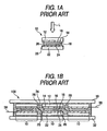
- Figs. 1A, 1B and 2 show a typical structure of a conventional dye sensitized solar cell module.
- Fig. 1A and 1B The structure shown in Fig. 1A and 1B have been disclosed in JP-A 2001-185743 Publication (Paragraph 0081) and JP-A 2003-86822 Publication, and individual finished dye sensitized solar cells 10 shown in Fig. 1A are connected in series through a connecting lead to obtain a module 100 as shown in Fig. 1B .
- the dye sensitized solar cell 10 in Fig. 1A is constituted by laminating, from a light receiving side of an incident light L (an upper part in the drawing), in order of a transparent substrate 12, a transparent conductive film 14, a dye carrying oxide semiconductor layer 16, an electrolyte layer 18, a back conductive film 20 (transparent or opaque) and a back substrate 22 (transparent or opaque).
- a catalyst layer 24 such as Pt or C is provided on the back conductive film 20, but this is not indispensable.
- the cell 10 is surrounded with a sealing material 26 in fluid tightness in order to prevent a leakage of the electrolyte 18.
- the back conductive film 20, extracting the electron (e-) from the outside, is functioning as a positive electrode of the cell 10.
- Fig. 1B shows the module 100 in which three dye sensitized solar cells 10 in Fig. 1A are arranged on a plane and connected in series.
- the positive electrode 20 and the negative electrode 14 in the adjacent cells 10 are electrically connected to each other through an electrode connecting wire 28 and are interposed between a transparent support substrate 30 and a back support substrate 32 (transparent or opaque), and are sealed with a transparent insulating filler 34 to obtain the module 100.
- An output terminal of the module 100 includes a positive electrode 36 and a negative electrode 38.
- JP-A 2002-93475 Publication has proposed a method of fabricating a module constituted by a plurality of cells in a batch as shown in Fig. 2 without depending on the assembly of the unit cell.
- a dye sensitized solar cell module 200 shown in Fig. 2 is fabricated in a batch as an integral structure in which a plurality of dye sensitized solar cells 210 and a plurality of intercell regions 215 are alternately arranged on a plane.
- the cell 210 has the same basic structure as that of the unit cell 10 in Fig. 1A and is constituted by laminating, from a light receiving side of an incident light L (an upper part in the drawing), in order of a transparent substrate 212, a transparent conductive film 214, a dye carrying oxide semiconductor layer 216, an electrolyte layer 218, a back conductive film 220 (transparent or opaque), and a back substrate 222 (transparent or opaque).
- a catalyst layer 224 such as Pt or C is provided on the back conductive film 220, which is, however, also not indispensable.
- the transparent substrate 212 or the back substrate 222 is eachmade from continuous single substrate which is common to all of the cells 210.
- the transparent conductive film 214 and the back conductive film 220 are constituted by electrode portions 214E and 220E provided in the cell 210 and extended portions 214T and 220T reaching an inner part of the intercell region 215 from the ends of the electrode portions, respectively.
- the transparent conductive film 214 feeding an electrode (e-) generated in the dye carrying oxide semiconductor layer 216 to an outside, is functioning as a negative electrode of the cell 210.
- the back conductive film 220 for extracting the electron (e-) from the outside is functioning as a positive electrode of the cell 210.
- the extended portion 214T of the negative electrode 214 of the cell 210 on a left side and the extended portion 220T of the positive electrode 220 of the cell 210 on a right side are electrically connected by an electrode connecting portion 228, which is individually provided in the intercell region 215.
- a height of the electrode connecting portion 228 defines a thickness of the electrolyte layer 218.
- a pair of intercell insulating barriers (or barrier walls) 226 are adhered to both sides of the electrode connecting portion 228 to carry out sealing in fluid tightness. Consequently, the electrolyte 218 is sealed in the cell 210 and a region of each cell 210 is defined.
- the electrode connecting portion 228 shall be formed in a gap surrounded by the intercell insulating barriers 226 at both sides, by which a complicated fabricating step is required.
- the dye sensitized solar cell has the greatest advantage in that a manufacturing cost can be reduced in addition to its low material cost.
- a manufacturing cost can be reduced in addition to its low material cost.
- the manufacturing costs of both the module structures shown in Figs. 1A, 1B and 2 are increased due to an increase in the number of module fabricating steps and the complicated fabrication steps.
- an electrode connecting portion is formed by a conductive material penetrating obliquely through an intercell insulating barrier as is disclosed in JP-A 2005-174679 publication, or a structure in which both cells are connected in series with a wire interposed between electrode extended portions of adjacent cells to insulate both sides of the wire with a glass frit as is disclosed in JP-A 2001-185244 publication.
- a method of forming an insulating barrier and an electrode connecting portion between adjacent cells does not show any concrete embodiment and might not be practical in use.
- a dye sensitized solar cell module 300 shown in Fig. 3 is fabricated in a batch as an integral structure in which regions of a plurality of dye sensitized solar cells 310 and a plurality of intercell regions 315 are alternately reversed on a plane.
- the cell 310 is constituted by laminating a first transparent substrate 312, a first transparent conductive film 314, a dye carrying oxide semiconductor layer 316, an electrolyte layer 318, a catalyst layer 324, a second transparent conductive film 320, and a second transparent substrate 322.
- the first transparent substrate 312 and the second transparent substrate 322 are continuous single substrates which are common to all of the cells 310, respectively.
- the first transparent conductive film 314 and the second transparent conductive film 320 are constituted by electrode portions 314E and 320E provided in the cell 310 and extended portions 314T and 320T reaching an inner part of the intercell region 315 from ends of the electrode portions 314E and 320E, respectively.
- the first transparent conductive film 314 feeding an electron (e-) generated in the dye carrying oxide semiconductor layer 316 to an outside, is functioning as a negative electrode, and, at the same time, said first transparent conductive film 314 is extended to the adjacent cell 310B to be functioning as a positive electrode for extracting the electron (e-) from the outside.
- a separate electrode connecting portion is not required.
- An insulating barrier (or barrier wall) 326 seals each cell 310 in fluid tightness. Consequently, the electrolyte 318 is sealed in the cell 310 so that a region of the individual cell 310 is defined.
- the dye carrying oxide semiconductor layer 316 of the cell 310A absorbs a light transmitted through the first transparent substrate 312 and the first transparent conductive film 314.
- the dye carrying oxide semiconductor layer 316 of the adjacent cell 310B absorbs the light that is further transmitted through the electrolyte 318 and the catalyst layer 324 such as Pt or C.
- the cell 310A and the cell 310B are simply reversed so that the same situation can be obtained.
- photoelectric converting efficiencies of the alternate cells 310 that is, half cells 310 are reduced. Therefore, it is impossible to avoid the reduction in the photoelectric converting efficiency as the whole dye sensitized solar cell module 300.
- JP 2000/124491 describes a solar battery module.
- a photoelectric conversion part where a first electrode, a photoelectric conversion layer and a second electrode are stacked on one face of an insulating substrate from a substrate side. Further, a back electrode is installed on the other face of the substrate. The second electrode and the back electrode are connected through a current collection hole passing through the substrate.
- WO 96/2971 describes a method of manufacturing a module of photoelectrochemical cells which contains a photosensitizer. Therein, two glass plates are connected to each other round their edges with an edge-sealing structure made from glass solder. The non-heat-resistant material is subsequently pumped into the sealed module through at least one suitably shaped feed aperture. Selective coating with glass solder enables linear ribs to be produced in order to form spatially discrete chambers.
- the invention provides a dye sensitized solar cell module in which a plurality of dye sensitized solar cells is arranged on a plane basis and is connected in series with an intercell region interposed therebetween, the dye sensitized solace cell is constituted by laminating a first transparent substrate, a first transparent conductive film, a dye carrying oxide semiconductor layer, an electrolyte layer, a catalyst layer, a second transparent conductive film and a second transparent substrate, each of the first transparent substrate and the second transparent substrate is a continuous single substrate which is common to all of the dye sensitized solar cells, the first transparent conductive film is constituted by an electrode portion provided in the cell and an extended portion reaching an inner part of the intercell region from one of ends of the electrode portion, the dye carrying oxide semiconductor layer is formed on the electrode portion of the first transparent conductive film, the second transparent conductive film is constituted by an electrode portion provided in the cell and an extended portion reaching an inner part of the intercell region from one of ends of the electrode portion, and the catalyst layer is formed on the
- a method of manufacturing the dye sensitized solar cell module according to the invention comprises the steps of:
- the structure of the dye sensitized solar cell module according to the invention it is possible to fabricate a plurality of cells on a single substrate in a batch while maintaining a high cell numerical aperture and a high photoelectric converting efficiency by simple steps of forming a barrier wall, forming a trench penetrating through the barrier wall from an outer surface of one of transparent substrates to reach a transparent conductive film on the other transparent substrate or a trench reaching an outer surface of the other transparent substrate, filling the trench with a conductive material.
- Embodiments are also directed to apparatuses manufactured by the disclosed methods and including apparatus parts corresponding to described method steps. Furthermore, embodiments are also directed to methods by which the described apparatus is manufactured. It may include method steps for manufacturing parts of the apparatus. The method steps may be performed by way of hardware components, firmware, software, a computer programmed by appropriate software, by any combination thereof or in any other manner.
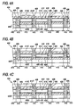
- Figs. 4A to 4C show the example of sectional structures of a dye sensitized solar cell module according to a preferred embodiment of the invention.
- a dye sensitized solar cell module 401 according to the invention shown in Fig. 4A is constituted by arranging a plurality of dye sensitized solar cells 410 on a plane basis and connecting them in series with an intercell region 415 interposed therebetween.
- a first transparent substrate 412, a first transparent conductive film 414, a dye carrying oxide semiconductor layer 416, an electrolyte layer 418, a catalyst layer 424, a second transparent conductive film 420 and a second transparent substrate 422 are laminated.
- the first transparent substrate 412 and the second transparent substrate 422 are continuous single substrates which are common to all of the dye sensitized solar cells 410, respectively.
- the first transparent conductive film 414 is constituted by an electrode portion 414E provided in the cell 410 and an extended portion 414T reaching an inner part of the intercell region 415 from one of ends of the electrode portion 414E.
- the dye carrying oxide semiconductor layer 416 is formed on the electrode portion 414E of the first transparent conductive film 414.
- the second transparent conductive film 420 is constituted by an electrode portion 420E provided in the cell 410 and an extended portion 420T reaching an inner part of the intercell region 415 from one of ends of the electrode portion 420E.
- the catalyst layer 424 is formed over the whole electrode portion 420E and extended portion 420T of the second transparent conductive film 420.
- the invention features that an insulating barrier 426 seals the cells 410 at both sides thereof in fluid tightness and insulates them and an electrode connecting portion 428 connects the extended portion 414T of the first transparent conductive film 414 of one of the cells 410 at both sides and the extended portion 420T of the second transparent conductive film 420 of the other cell 410 in the intercell region 415.
- the electrode connecting portion 428 penetrates through the second transparent substrate 422 in a vertical direction and is exposed to an outer surface of the second transparent substrate 422.
- Embodiments shown in Figs. 4B and 4C have the same structure as that of the embodiment in Fig. 4A except that the electrode connecting portion 428 penetrates through any of the first and second transparent substrates. More specifically, in the case of the embodiment shown in Fig. 4B , the electrode connecting portion 428 penetrates through the first transparent substrate 412 in the vertical direction and is exposed to the outer surface of the first transparent substrate 412. In the case of the embodiment in Fig. 4C , the electrode connecting portion 428 penetrates through both the first transparent substrate 412 and the second transparent substrate 422 in the vertical direction and is exposed to the outer surface of the first transparent substrate 412 and that of the second transparent substrate 422.
- Figs. 5A to 5C show the examples of sectional structures of a dye sensitized solar cell module according to a further preferred embodiment of the invention.
- Dye sensitized solar cell modules 401A, 402A and 403A shown in Figs. 5A, 5B and 5C have features that a first auxiliary conductive layer 430 and a second auxiliary conductive layer 432 are added to the extended portion 414T of the first transparent conductive film 414 and the extended portion 420T of the second transparent conductive film 420 which are connected to the electrode connecting portion 428 respectively in the structures of the dye sensitized solar cell modules 401, 402 and 403 shown in Figs. 4A, 4B and 4C .
- the first auxiliary conductive layer 430 is added to compensate for a thickness of the first transparent conductive film 414 to be connected to a tip surface of the electrode connecting portion 428, thereby maintaining a conduction of the first transparent conductive film 414 and the electrode connecting portion 428 more stably.
- the second auxiliary conductive layer 432 is added to increase a sectional area of a second conductive film and the catalyst layer 424 to be connected to a side surface of the electrode connecting portion 428, thereby maintaining a conduction of the second transparent conductive film 420 and the electrode connecting portion 428 more stably.
- a first auxiliary conductive layer 430 compensates for a thickness of a first transparent conductive film 414 to be connected to a side surface of the electrode connecting portion 428, thereby maintaining their conduction stably
- a second auxiliary conductive layer 432 compensates for a thickness of a second conductive film 420 (constituting an integral portion with a catalyst layer 424) to be connected to a tip surface of the electrode connecting portion 428, thereby maintaining their conduction stably.
- a first auxiliary conductive layer 430 compensates for a thickness of a first transparent conductive film 414 to be connected to a side surface of the electrode connecting portion 428, thereby maintaining their conduction stably
- a second auxiliary conductive layer 432 compensates for a thickness of a second transparent conductive film 420 (constituting an integral portion with the catalyst layer 424) to be connected to a side surface of the electrode connecting portion 428, thereby maintaining their conduction stably.
- the dye sensitized solar cell module according to each of the embodiments shown in Figs. 4A, 4B and 4C can be manufactured by the same method.
- a manufacturing method will be described below by setting the case of the embodiment shown in Fig. 4A to be a typical example.
- Figs. 6A to Fig. 12D sequentially show the manufacturing steps thereof.
- a first transparent conductive film 414 is formed over a whole surface of a first transparent substrate 412. It is possible to use a product put on the market (A110U80 manufactured by Asahi Glass Company) in a state in which the FTO (fluorine-doped tin oxide) film 414 is formed on the glass substrate 412.
- a thickness of the first transparent conductive film 414 is equal to or greater than 0.1 ⁇ m and is usually approximately 0.3 to 2 ⁇ m.
- SnO 2 tin oxide
- ATO antimony-doped tin oxide
- In 2 O 3 indium oxide
- ITO indium - tin composite oxide
- MgO manganesium oxide
- ZnO zinc oxide
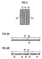
- a plurality of first trenches 441 having a width of approximately 100 to 300 nm is formed on the first transparent conductive film (FTO film) 414 in parallel with each other by a YAG laser. Consequently, the first transparent conductive film 414 is divided into a plurality of straps having a width of 10 mm X a length of 100 mm as shown in a plan view of Fig. 7 , for example.
- Fig. 6B is a sectional view taken along a line A - A shown in Fig. 7 .
- a dye carrying oxide semiconductor layer 416 is formed in a region (that is, an electrode portion 414E) other than an extended portion 414T provided on each first transparent conductive film 414 thus divided.
- Fig. 8 is a plan view.
- Fig. 6C is a sectional view taken along a line A - A shown in Fig. 8 .
- the dye carrying oxide semiconductor layer 416 is formed in the following manner, for example.
- a TiO 2 paste (manufactured by Catalysts & Chemicals Industries Co., Ltd. : DST - 18NR) is subjected to screen printing, and is then dried and burned (450°C X 30 minutes) to form a porous TiO 2 semiconductor layer having a thickness of 15 ⁇ m in a width of 8 mm X a length of 95 mm (the case in which the first transparent conductive film 414 has a width of 10 mm X a length of 100 mm).
- the porous TiO 2 semiconductor layer is caused to adsorb a dye so that the dye carrying oxide semiconductor layer 416 is finished.
- the dye adsorption is carried out in the following manner, for example.
- the first transparent substrate 412 having the porous TiO 2 semiconductor layer formed on the first transparent conductive film 414 is dipped in a solution of a sensitizing dye expressed in [Ru (4, 4' - dicarboxyl - 2, 2' - bipyridine) 2 - (NCS) 2 ] and is left for 24 hours at a room temperature.
- a sensitizing dye solution there is used a solution obtained by containing, in a concentration of 3 X 10 -4 mol/dm -3 , the sensitizing dye in a mixed solvent of acetonitrile and t-butanol at a volume ratio of 50 : 50.
- ZnO zinc oxide
- SnO 2 tin oxide
- In 2 O 3 indium oxide
- Nb 2 O 5 niobium oxide
- WO 3 tungsten oxide
- ZrO 2 zirconium oxide
- La 2 O 3 lanthanum oxide
- Ta 2 O 5 tantalum oxide
- SrTiO 3 sinrontium titanate
- BaTiO 3 barium titanate
- a first board 451 on a light receiving side is obtained.
- a second transparent conductive film 420 and a catalyst layer 424 are sequentially formed over a whole surface of a second transparent substrate 422. This is carried out by forming, on the ITO film 420, the Pt catalyst layer 424 in a thickness of 200 to 1000 nm by sputtering using a product put on the market (manufactured by TOBI CO., LTD. : a PEN (polyethylene naphthalate) film [a film thickness of 125 ⁇ m]) in a state in which the ITO film 420 is formed on the resin film substrate 422.
- a PEN polyethylene naphthalate
- FTO fluorescence-to-doped tin oxide
- ATO antimony-doped tin oxide
- In 2 O 3 indium oxide
- MgO manganesium oxide
- ZnO zinc oxide
- PET polyethylene terephthalate
- polycarbonate polypropylene
- polyamide polyamide
- a cycloolefin polymer polyether sulfine and polymethyl methacrylate
- materials having a high resistance to an electrolyte and an excellent light transmitting property for example, the PET and the polycarbonate are desirable.
- the listed materials do not need to be restricted.
- a plurality of parallel second trenches 442 is formed on a united layer [420 + 424] of the second transparent conductive film 420 and the catalyst layer 424 by etching using an etchant containing hydrochloric acid as a main body, and the united layer [420 + 424] is divided into a plurality of straps.
- Fig. 10 is a plan view.
- Fig. 9B is a sectional view taken along a line A - A shown in Fig. 10 .
- an insulating material 426' for a barrier is disposed in an intercell region 415 constituted by the first trench 441 dividing the first transparent conductive film 414 and the extended portion 414T of the first transparent conductive film 414 in the first board 451.
- the extendedportion 414T of the first transparent conducive film 414 in a cell region 410 and an extended portion Toftheunitedlayer [420+424] of the second transparent conductive film 420 and the catalyst layer 424 in an adjacent cell region 410 should be disposed to overlap each other over a plan view.
- a thermoplastic resin manufactured by Du Pont Co., Ltd. : HIMILAN 1702
- the second trench 442 dividing the united layer [420 + 424] of the second transparent conductive film 420 and the catalyst layer 424 in the second board 452 is aligned with the insulating material 426' provided above the first board 451 and are caused to face each other so that the insulating material 426' for a barrier is interposed between the first board 451 and the second board 452.
- the second board 452 is superposed on the first board 451 and they are subjected to thermocompression bonding at approximately 100°C.
- a space between both of the boards 451 and 452 in the intercell region 415 is filled with the insulating material 426' for a barrier to form a barrier wall 426".
- the barrier walls 426" are functioning as sand witching and sealing the electrolyte layers as will be explained later on.
- the insulating material 426' for a barrier a material having a necessary property such as an insulating property, a corrosion resistance to an electrolyte 418 or a mechanical strength is suitable, and a thermosetting resin and a light-curing resin can be used in addition to the thermoplastic resin described above.
- thermoplastic resin an ionomer resin, an EVA resin (an Ethylene-Vinyl Acetate (ethylene - vinyl acetate) copolymer resin), a polyacetal resin, a vinyl chloride resin, an acrylic resin and a phenol resin are typical in addition to the specific examples, and they do not need to be restricted.
- EVA resin an Ethylene-Vinyl Acetate (ethylene - vinyl acetate) copolymer resin
- polyacetal resin a vinyl chloride resin
- acrylic resin and a phenol resin a phenol resin
- thermosetting resin an epoxy resin, a phenol resin and a diallyl phthalate resin are typical and do not need to be restricted.
- An ultraviolet curing epoxy resin and an ultraviolet curing acrylic resin are typical for the light-curing resin and do not need to be restricted.
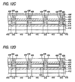
- a third trench 443 penetrating through the barrier wall 426" from an outer surface of the second transparent substrate (resin film substrate) 422 of the second board 452 and reaching the extended portion 414T of the first transparent conductive film (FTO) 414 of the first board 451 is formed by means of a YAG laser.
- the third trench 443 has a width of 50 to 500 ⁇ m and a length of 90 mm, for example. Consequently, there is formed an insulating barrier 426 for sealing the cells 410 on both sides of the intercell region 415 in fluid tightness and insulating them.
- electroless copper plating is carried out after nonelectroless copper plating, and a whole inner part of the third trench 443 is filled with a copper 428' to be a conductive material as shown in a section of Fig. 12C .
- a copper 428' is filled with a copper 428' to be a conductive material as shown in a section of Fig. 12C .
- portions other than an outer surface of the second transparent substrate 422 and an inner surface of the third trench 443 are masked with a tape to prevent the plating.
- an electrolyte is injected from an inlet (not shown) by a pressure reduction injecting method so as to form electrolyte layers of the cell and the dye sensitized solar cell module 401 shown in Fig. 4A is finished.
- a 3-methoxypropionitrile solution containing 0.5 M lithium iodide, 0.05 M iodine and 0.01M4 - tert - butylpyridine is used.
- the dye sensitized solar cell module 402 shown in Fig. 4B can also be manufactured by the same manufacturing process as that in the example 1.
- a third trench 443 is formed on a first transparent substrate 412 comprising a dye carrying oxide semiconductor layer 416 by digging through a YAG laser. Therefore, the glass substrate used in the example 1 has a poor laser processability and is unstable for the first transparent substrate 412. Instead, a material having an excellent laser processability, for example, a resin film substrate used as a second transparent substrate 422 is utilized.
- the third trench 443 is formed to penetrate through a barrier wall 426" from an outer surface of a first board 451 and to reach a second transparent conductive film 420 of a second board 452.
- a dye sensitized solar cell module 403 shown in Fig. 4C can also be manufactured by the same manufacturing process as that in the example 1.
- a third trench 443 is formed on both a first transparent substrate 412 and a second transparent substrate 422 by digging through a YAG laser.
- a material having an excellent laser processability for example, the same resin film substrate as the second transparent substrate 422 is also used for the first transparent substrate 412.
- the third trench 443 penetrating through a barrier wall 426" from an outer surface of one of a first board 451 and a second board 452 and reaching an outer surface of the other is formed.
- the dye sensitized solar cell modules 401A, 402A and 403A according to the respective embodiments in Figs. 5A, 5B and 5C can be manufactured by the same methods as those for the dye sensitized solar cell modules 401, 402 and 403 according to the examples 1, 2 and 3, respectively.
- a manufacturing method will be described below by setting the dye sensitized solar cell module 401A in Fig. 5A to be a typical example.
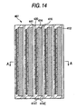
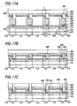
- Figs. 13A to 17E sequentially show a manufacturing process. An operation for forming the auxiliary conductive layers 430 and 432 is simply added to the manufacturing method described in the example 1.
- an auxiliary conductive layer 430 is formed on an extended portion 414T of a first transparent conductive film 414. This is carried out by screen printing for an Ag paste and drying, for example.
- the auxiliary conductive layer 430 is set to have a width of 0.5 mm X a length of 95 mm and a film thickness of 4 ⁇ m or more. The width and the length of the auxiliary conductive layer 430 are set within such a range as not to deteriorate the fluid-tight sealing and insulating functions of the insulating barrier 426 ( Fig. 5A ).
- a first board 461 on a light receiving side is obtained.
- auxiliary conductive layer 432 is formed on a side edge of a second transparent conductive film 420 + a catalyst layer 424 which finally acts as an extended portion 420T.
- the auxiliary conductive layer 430 is set to have a width of 0.5 mm X a length of 95 mm and a film thickness of 4 ⁇ m or more. The width and the length of the auxiliary conductive layer 430 are set within such a range as not to deteriorate the fluid-tight sealing and insulating functions of the insulating barrier 426 ( Fig. 5A ).
- an insulating material 426' for a barrier is disposed in an intercell region 415 constituted by a first trench 441 dividing a first transparent conductive film 414 and an extended portion 414T of the first transparent conductive film 414 in the first board 461.
- the extended portion 414T of the first transparent conductive film 414 in a cell region 410 and an extended portion T of a united layer [420+424] of the second transparent conductive film 420 and the catalyst layer 424 in an adjacent cell region 410 should be disposed to overlap each other over a plan view.
- thermoplastic resin manufactured by Du Pont Co., Ltd. : HIMILAN 1702
- a thermosetting resin and a light-curing resin in addition to a thermoplastic resin.
- a second trench 442 dividing the united layer [420 + 424] of the second transparent conductive film 420 and the catalyst layer 424 in the second board 462 is aligned with the insulating material 426' for a barrier which is provided above the first board 461 and they are caused to face each other so that the insulating material 426' for a barrier is interposed between the first board 461 and the second board 462.
- the second board 462 is superposed on the first board 461 and they are subj ected to thermocompression bonding at approximately 100°C.
- a space between both of the boards 461 and 462 in the intercell region 415 are filled with the insulating material 426' for a barrier to form a barrier wall 426".
- a third trench 443 penetrating through the barrier wall 426" from an outer surface of a second transparent substrate (resin film substrate) 422 of the second board 462 and reaching the auxiliary conductive layer 430 provided on the extended portion 414T of the first transparent conductive film (FTO) 414 of the first board 461 is formed by means of a YAG laser.
- the auxiliary conductive layer 432 of the second board 462 is exposed to a side surface of the third trench 443.
- the third trench 443 has a width of 50 to 500 ⁇ m and a length of 90 mm, for example. Consequently, there is formed an insulating barrier 426 for sealing the cells 410 on both sides of the intercell region 415 in fluid tightness and insulating them.
- electroless copper plating is carried out after nonelectroless copper plating, and a whole inner part of the third trench 443 is filled with a copper 428' to be a conductor material as shown in a section of Fig. 17D .
- portions other than an outer surface of the second transparent substrate 422 and an inner surface of the third trench 443 are masked with a tape to prevent the plating.
- the same electrolyte as that in the example 1 is injected from an inlet (not shown) by a pressure reduction injecting method so that the dye sensitized solar cell module 401A shown in Fig. 5A is finished.
- the intercell region 415 is illustrated in a higher relative ratio than actual one with respect to the cell region 410 for convenience of the drawings.
- the actual intercell regions 415 and 515 may be considerably smaller than those in the drawings. Therefore, it is possible to maintain a very high cell numerical aperture.
- a solar cell module in which a plurality of dye sensitized solar cells is arranged on a plane basis and is connected in series with an intercell region interposed therebetween, a first transparent substrate, a first transparent conductive film, a dye carrying oxide semiconductor layer, an electrolyte layer, a catalyst layer, a second transparent conductive film and a second transparent substrate are laminated, an insulating barrier seals cells on both sides thereof in fluid tightness and insulates them in the intercell region, an electrode connecting portion provided in a central part in a vertical direction of the insulating barrier connects an extended portion of the first transparent conductive film of one of the cells on the both sides to that of a second transparent conductive film of the other cell, and the electrode connecting portion penetrates through at least one of the first transparent substrate and the second transparent substrate in the vertical direction and is thus exposed.
- a dye sensitized solar cell module which has a high cell numerical aperture and a high photoelectric converting efficiency, and at the same time, has a structure improved to fabricate a plurality of cells on a single substrate in a batch without requiring a complicated step, and a method of manufacturing the dye sensitized solar cell module.
Landscapes
- Engineering & Computer Science (AREA)
- Power Engineering (AREA)
- Chemical & Material Sciences (AREA)
- Chemical Kinetics & Catalysis (AREA)
- Electrochemistry (AREA)
- Microelectronics & Electronic Packaging (AREA)
- Hybrid Cells (AREA)
- Photovoltaic Devices (AREA)
- Connection Of Batteries Or Terminals (AREA)
- Sealing Battery Cases Or Jackets (AREA)
Claims (8)
- Ein farbstoffsensibilisiertes Solarzellenmodul (401, 402, 403, 401A, 402A, 403A), in welchem eine Vielzahl von farbstoffsensibilisierten Solarzellen (410) nebeneinander angeordnet und mit einem dazwischen angeordneten Zwischenzellenbereich (415) in Reihe geschaltet sind, wobei jede der Vielzahl von farbstoffsensibilisierten Solarzellen umfasst:ein erstes gemeinsames transparentes Substrat (412), welches ein kontinuierliches einzelnes transparentes Substrat ist und gemeinsam für jedes der anderen der Vielzahl von farbstoffsensibilisierten Solarzellen verwendet wird;eine erste transparente leitfähige Schicht (414), welche auf dem ersten transparenten Substrat ausgebildet ist, gebildet durch einen in einem Zellenbereich bereitgestellten ersten Elektrodenbereich (414E) und einen ersten verlängerten Bereich (414T), welcher sich von einem Ende des ersten Elektrodenbereichs zu einem inneren Teil des Zwischenzellenbereichs erstreckt;eine farbstofftragende Oxid-Halbleiter-Schicht (418), die auf dem ersten Elektrodenbereich der ersten transparenten leitfähigen Schicht ausgebildet ist;ein zweites gemeinsames transparentes Substrat (422), welches ein kontinuierliches einzelnes transparentes Substrat ist und gemeinsam für jedes der anderen der Vielzahl von farbstoffsensibilisierten Solarzellen verwendet wird;eine zweite transparente leitfähige Schicht (420), welche auf dem zweiten gemeinsamen transparenten Substrat ausgebildet ist, gebildet durch einen in den Zellenbereich bereitgestellten zweiten Elektrodenbereich (420E) und einen zweiten verlängerten Bereich (420T), welcher sich von einem Ende des zweiten Elektrodenbereichs zu einem inneren Teil des Zwischenzellenbereichs erstreckt;eine Katalysatorschicht (424), die integral auf dem zweiten Elektrodenbereichs und dem zweiten verlängerten Bereich der zweiten transparenten leitfähigen Schicht gebildet ist, undeine Elektrolytschicht (418), die zwischen der farbstofftragenden Oxid-Halbleiter-Schicht und der Katalysatorschicht bereitgestellt ist, wobeieine isolierende Barriere (426) auf jeder Seite des Zellenbereichs bereitgestellt ist, um den Zellenbereich unter Wahrung von Fluiddichtheit des Zellenbereichs abzudichten, und wobeiferner ein Elektrodenverbindungsbereich (428) vertikal zwischen der isolierenden Barriere des Zellenbereichs und einer isolierenden Barriere von einem anderen dazu benachbarten Zellenbereich bereitgestellt ist, um die erste transparente leitfähige Schicht der Zelle und die zweite transparente leitfähige Schicht der anderen Zelle elektrisch zu verbinden, und wobei der Elektrodenverbindungsbereichzumindest einen von verlängerten Bereichen des ersten transparenten Substrats und des zweiten transparenten Substrats in der vertikalen Richtung durchdringt, um extern exponiert zu sein.
- Das farbstoffsensibilisierte Solarzellenmodul nach Anspruch 1, wobei einer der verlängerten Bereiche (414T, 420T) der ersten transparenten leitfähigen Schicht (414) und der zweiten transparenten leitfähigen Schicht (420) eine erste zusätzliche leitfähige Schicht (430) und beziehungsweise eine zweite zusätzliche leitfähige Schicht (432) umfasst.
- Ein Verfahren zur Herstellung des farbstoffsensibilisierten Solarzellenmoduls nach Anspruch 1, umfassend:Herstellen eines ersten Boards durch Ausbilden einer ersten transparenten leitenden Schicht (414) über einem ersten transparenten Substrat (412), Ausbilden einer Vielzahl von ersten Vertiefungen auf der ersten transparenten leitfähigen Schicht, um so die erste transparente leitfähige Schicht in eine Vielzahl von einzelnen ersten transparenten leitfähigen Schichten zu unterteilen, und Ausbilden von farbstofftragenden Oxid-Halbleiter-Schichten auf anderen Bereichen als auf verlängerten Bereichen (414T) der jeweiligen einzelnen ersten transparenten leitfähigen Schichten;Herstellen eines zweiten Boards durch Ausbilden einer zweiten transparenten leitfähigen Schicht (420) über ein zweites transparentes Substrat (422) mit Ausbilden einer Katalysatorschicht darauf, Ausbilden einer Vielzahl von zweiten Vertiefungen in Schichten der zweiten transparenten leitfähigen Schicht und der Katalysatorschicht, um so die Schichten in eine Vielzahl von Teilen zu unterteilen;Anordnen von isolierendem Material, das als Barriere für die Zwischenzellenbereiche (415) fungiert, wobei jeder der Zwischenzellenbereiche durch eine der ersten Vertiefungen und der verlängerten Bereiche von irgendeiner der einzelnen ersten transparenten leitfähigen dazu entsprechenden Schichten bestimmt wird;Anordnen des zweiten Boards auf dem ersten Board in einer Weise, dass die zweiten Vertiefungen mit den entsprechenden Isoliermaterialien auf dem ersten Board ausgerichtet und einander zugewandt sind, wodurch Räume in den Zwischenzellenbereichen zwischen den beiden Boards mit dem isolierenden Material ausgefüllt werden, um Barrierewände zu bilden;Durchführen irgendeines der Prozesse (i), (ii), (iii) in irgendeinem der Zwischenzellenbereiche:(i) Ausbilden einer dritten Vertiefung, die die Barrierewand von einer äußeren Oberfläche des ersten Boards durchdringt und die zweite transparente leitfähigen Schicht des zweiten Boards erreicht;(ii) Ausbilden einer dritten Vertiefung, die die Barrierewand von einer äußeren Oberfläche des zweiten Boards durchdringt und die erste transparente leitfähige Schicht des ersten Boards erreicht;(iii) Ausbilden einer dritten Vertiefung, die die Barrierewand von einer äußeren Oberfläche irgendeiner des ersten Boards und des zweiten Boards durchdringt und die äußere Oberfläche der anderen erreicht, wodurch ein Paar von isolierenden Barrieren gebildet wird, um eine dazwischen angeordnete Zelle unter Wahrung von Fluiddichtheit abzudichten; undFüllen eines gesamten inneren Teils der dritten Vertiefung mit leitfähigem Material, wodurch ein Elektrodenverbindungsbereich zum elektrischen Verbinden der ersten transparenten leitfähigen Schicht der Zelle und der zweiten transparenten leitfähigen Schicht einer anderen Zelle gebildet wird.
- Das Verfahren zur Herstellung eines farbstoffsensibilisierten Solarzellenmoduls nach Anspruch 3, ferner umfassend:Ausbilden einer ersten zusätzlichen leitfähigen Schicht (430) in dem verlängertem Bereich der ersten transparenten leitfähigen Schicht nach dem Schritt des Herstellens des ersten Boards und vor dem Schritt des Anordnens des Isoliermaterials für eine Barriere; undAusbilden einer zweiten zusätzlichen leitfähigen Schicht (432) in einem verlängerten Bereich der vereinten Schicht der zweiten transparenten leitfähigen Schicht, und der Katalysatorschicht nach dem Schritt des Herstellens des zweiten Boards und vor dem Schritt des Bildens der Barrierewand.
- Das farbstoffsensibilisierte Solarzellenmodul (401, 402, 403, 401A, 402A, 403A) nach einem der vorhergehenden Ansprüche, ferner umfassend:eine erstes Board umfassend das erste gemeinsame transparente Substrat (412);eine zweites Board umfassend das zweite gemeinsame transparente Substrat (422).
- Das farbstoffsensibilisierte Solarzellenmodul nach Anspruch 5, wobei jede der Vielzahl der ersten transparenten leitfähigen Schichten durch einen in einem Zellenbereich bereitgestellten ersten Elektrodenbereich und einen ersten verlängerten Bereich gebildet wird, welcher sich von einem Ende des zweiten Elektrodenbereichs zu einem der inneren Teile des Zwischenzellenbereichs erstreckt, und jede der farbstofftragenden Oxid-Halbleiter-Schichten auf dem ersten Elektrodenbereich desselben ausgebildet ist.
- Das farbstoffsensibilisierte Solarzellenmodul nach einem der Ansprüche 5 bis 6, wobei jede der zweiten transparenten leitfähigen Schichten durch einen in dem Zellenbereich bereitgestellten zweiten Elektrodenbereich und einen zweiten verlängerten Bereich gebildet wird, der denjenigen von den inneren Teilen des Zwischenzellenbereichs von einem Ende des zweiten Elektrodenbereichs erreicht, und jede der Katalysatorschichten integral auf dem zweiten Elektrodenbereich und dem zweiten verlängerten Bereich des zweiten transparenten leitfähigen Films ausgebildet ist.
- Das farbstoffsensibilisierte Solarzellenmodul nach einem der Ansprüche 6 bis 7, wobei einer der verlängerten Bereiche der ersten transparenten leitfähigen Schicht und derjenige der zweiten transparenten leitfähigen Schicht eine erste zusätzliche leitfähige Schicht (430) und beziehungsweise eine zweite zusätzliche leitfähige Schicht (432) umfasst.
Applications Claiming Priority (1)
| Application Number | Priority Date | Filing Date | Title |
|---|---|---|---|
| JP2006338456A JP5089157B2 (ja) | 2006-12-15 | 2006-12-15 | 色素増感型太陽電池モジュールおよびその製造方法 |
Publications (3)
| Publication Number | Publication Date |
|---|---|
| EP1933344A2 EP1933344A2 (de) | 2008-06-18 |
| EP1933344A3 EP1933344A3 (de) | 2012-07-25 |
| EP1933344B1 true EP1933344B1 (de) | 2014-02-12 |
Family
ID=39294050
Family Applications (1)
| Application Number | Title | Priority Date | Filing Date |
|---|---|---|---|
| EP07024411.6A Ceased EP1933344B1 (de) | 2006-12-15 | 2007-12-17 | Farbstoffsensibilisiertes Solarzellenmodul und Herstellungsverfahren dafür |
Country Status (3)
| Country | Link |
|---|---|
| US (1) | US7977569B2 (de) |
| EP (1) | EP1933344B1 (de) |
| JP (1) | JP5089157B2 (de) |
Families Citing this family (30)
| Publication number | Priority date | Publication date | Assignee | Title |
|---|---|---|---|---|
| KR20100075552A (ko) * | 2007-11-02 | 2010-07-02 | 니폰 가야꾸 가부시끼가이샤 | 색소 증감 태양전지 모듈 |
| US7994418B2 (en) * | 2008-09-18 | 2011-08-09 | General Electric Company | Monolithically connected photovoltaic devices on flexible substrates |
| KR101071699B1 (ko) | 2008-12-11 | 2011-10-11 | 주식회사 이건창호 | 염료감응형 태양전지 |
| JP5362379B2 (ja) * | 2009-02-06 | 2013-12-11 | 三洋電機株式会社 | 太陽電池のi−v特性の測定方法 |
| WO2010109821A1 (ja) * | 2009-03-26 | 2010-09-30 | 新日鐵化学株式会社 | 光電変換素子 |
| JP4868058B2 (ja) * | 2009-11-16 | 2012-02-01 | 大日本印刷株式会社 | 色素増感型太陽電池 |
| KR101108186B1 (ko) * | 2010-01-08 | 2012-01-31 | 삼성에스디아이 주식회사 | 광전변환모듈 |
| US8669468B2 (en) | 2010-01-19 | 2014-03-11 | Samsung Sdi Co., Ltd. | Photoelectric conversion module |
| US8587081B2 (en) * | 2010-04-28 | 2013-11-19 | Calvin Yi-Ping Chao | Back side illuminated image sensor with back side pixel substrate bias |
| KR101137378B1 (ko) * | 2010-07-16 | 2012-04-20 | 삼성에스디아이 주식회사 | 염료감응 태양전지 |
| KR101050471B1 (ko) * | 2010-07-19 | 2011-07-19 | 삼성에스디아이 주식회사 | 광전 변환 모듈 |
| KR101032916B1 (ko) * | 2010-08-10 | 2011-05-06 | 주식회사 티지에너지 | 염료감응 태양전지 직렬구조 셀 |
| KR101144038B1 (ko) * | 2010-11-11 | 2012-05-24 | 현대자동차주식회사 | 곡면형 염료감응 태양전지 및 그 제조방법 |
| DE102011001061B4 (de) * | 2011-03-03 | 2017-10-05 | Solarworld Innovations Gmbh | Solarzellenverbinder-Elektrode, Solarzellenmodul und Verfahren zum elektrischen Verbinden mehrerer Solarzellen |
| JP2012227063A (ja) * | 2011-04-21 | 2012-11-15 | Dainippon Printing Co Ltd | 色素増感型太陽電池素子モジュール |
| KR20130055439A (ko) * | 2011-11-18 | 2013-05-28 | 삼성에스디아이 주식회사 | 광전변환소자 |
| JP5929118B2 (ja) * | 2011-11-21 | 2016-06-01 | 大日本印刷株式会社 | フレキシブル太陽電池素子モジュール |
| SE537669C2 (sv) * | 2012-04-04 | 2015-09-29 | Exeger Sweden Ab | Färgämnessensiterad solcellsmodul med seriekopplad struktursamt sätt för framställning av solcellen |
| JP5444488B1 (ja) * | 2012-09-01 | 2014-03-19 | 株式会社フジクラ | 色素増感太陽電池素子 |
| US9947483B2 (en) | 2012-09-01 | 2018-04-17 | Fujikura Ltd. | Dye-sensitized solar cell element |
| CN104428858B (zh) * | 2012-10-19 | 2017-06-20 | 积水化学工业株式会社 | 电气模块 |
| JP6000808B2 (ja) * | 2012-11-06 | 2016-10-05 | 日本写真印刷株式会社 | 色素増感型太陽電池モジュール |
| KR101449301B1 (ko) | 2013-06-14 | 2014-10-17 | 현대자동차주식회사 | 누설전류 차단형 염료감응 태양전지 어레이 |
| WO2015008227A1 (en) * | 2013-07-15 | 2015-01-22 | 3Gsolar Photovoltaics Ltd. | Plastic solar dye cells |
| US20150020863A1 (en) * | 2013-07-22 | 2015-01-22 | International Business Machines Corporation | Segmented thin film solar cells |
| CN103680989A (zh) * | 2013-09-29 | 2014-03-26 | 营口奥匹维特新能源科技有限公司 | 光阳极、对电极及其形成的染料敏化太阳能电池 |
| WO2015125609A1 (ja) * | 2014-02-19 | 2015-08-27 | 株式会社村田製作所 | 光発電モジュール |
| CN112582547A (zh) * | 2016-03-30 | 2021-03-30 | 日本瑞翁株式会社 | 有机系太阳能电池 |
| JP7386595B2 (ja) * | 2018-04-05 | 2023-11-27 | 新光電気工業株式会社 | 配線基板、半導体装置及び配線基板の製造方法 |
| CN113381287A (zh) * | 2021-06-09 | 2021-09-10 | 中国科学院微电子研究所 | 一种染料激光器及其制备方法 |
Family Cites Families (20)
| Publication number | Priority date | Publication date | Assignee | Title |
|---|---|---|---|---|
| JPS60123073A (ja) * | 1983-12-08 | 1985-07-01 | Fuji Electric Corp Res & Dev Ltd | 薄膜太陽電池 |
| CH674596A5 (de) | 1988-02-12 | 1990-06-15 | Sulzer Ag | |
| JPH0815097A (ja) | 1994-06-30 | 1996-01-19 | Shimadzu Corp | タイヤ検査システム |
| DE4425193C1 (de) | 1994-07-16 | 1995-11-09 | Bosch Gmbh Robert | Drehzahlverstellbarer EC-Gleichstrommotor |
| DE19680102B4 (de) * | 1995-03-23 | 2007-04-12 | Ecole polytechnique fédérale de Lausanne (EPFL) | Verfahren zum Herstellen eines langzeitstabilen Moduls von photoelektrischen Zellen |
| JP3551787B2 (ja) * | 1998-10-14 | 2004-08-11 | 富士電機アドバンストテクノロジー株式会社 | 太陽電池モジュールおよびその製造方法 |
| JP2001185743A (ja) | 1999-12-22 | 2001-07-06 | Fuji Photo Film Co Ltd | 光電変換素子および太陽電池 |
| JP4414036B2 (ja) | 1999-12-27 | 2010-02-10 | シャープ株式会社 | 色素増感型太陽電池の作製方法 |
| US6706963B2 (en) * | 2002-01-25 | 2004-03-16 | Konarka Technologies, Inc. | Photovoltaic cell interconnection |
| JP4659954B2 (ja) * | 2000-09-19 | 2011-03-30 | 大日本印刷株式会社 | 色素増感型太陽電池セルの製造方法及び色素増感型太陽電池モジュールの製造方法 |
| JP2003086822A (ja) | 2001-09-10 | 2003-03-20 | Aisin Seiki Co Ltd | 太陽電池モジュール及びその製造方法 |
| JP4601282B2 (ja) * | 2003-11-07 | 2010-12-22 | 大日本印刷株式会社 | 色素増感型太陽電池用電極基板及びその製造方法、並びに色素増感型太陽電池 |
| JP4411955B2 (ja) | 2003-12-10 | 2010-02-10 | パナソニック電工株式会社 | 光電変換素子モジュール |
| US7781672B2 (en) * | 2004-06-01 | 2010-08-24 | Konarka Technologies, Inc. | Photovoltaic module architecture |
| US7276724B2 (en) * | 2005-01-20 | 2007-10-02 | Nanosolar, Inc. | Series interconnected optoelectronic device module assembly |
| JP4787540B2 (ja) * | 2005-05-20 | 2011-10-05 | Jx日鉱日石エネルギー株式会社 | 色素増感型太陽電池素子の製造方法 |
| JP2007066875A (ja) * | 2005-08-02 | 2007-03-15 | Ngk Spark Plug Co Ltd | 色素増感型太陽電池 |
| JP2007165137A (ja) * | 2005-12-14 | 2007-06-28 | Shinko Electric Ind Co Ltd | 絶縁隔壁の形成方法 |
| JP2007173045A (ja) | 2005-12-22 | 2007-07-05 | Shinko Electric Ind Co Ltd | 色素増感型太陽電池モジュールおよびその製造方法 |
| JP5032051B2 (ja) * | 2006-04-17 | 2012-09-26 | 日本特殊陶業株式会社 | 色素増感型太陽電池 |
-
2006
- 2006-12-15 JP JP2006338456A patent/JP5089157B2/ja not_active Expired - Fee Related
-
2007
- 2007-12-10 US US11/953,457 patent/US7977569B2/en not_active Expired - Fee Related
- 2007-12-17 EP EP07024411.6A patent/EP1933344B1/de not_active Ceased
Also Published As
| Publication number | Publication date |
|---|---|
| JP2008153013A (ja) | 2008-07-03 |
| EP1933344A2 (de) | 2008-06-18 |
| US20080236662A1 (en) | 2008-10-02 |
| US7977569B2 (en) | 2011-07-12 |
| EP1933344A3 (de) | 2012-07-25 |
| JP5089157B2 (ja) | 2012-12-05 |
Similar Documents
| Publication | Publication Date | Title |
|---|---|---|
| US7977569B2 (en) | Dye sensitized solar cell module and manufacturing method thereof | |
| EP2287961B1 (de) | Modul aus fotoelektrischen umwandlungselementen und verfahren zur herstellung eines moduls aus fotoelektrischen umwandlungselementen | |
| EP2683020B1 (de) | Farbstoffsensibilisiertes solarzellenmodul | |
| CN102792518B (zh) | 染料敏化太阳能电池模块及其制造方法 | |
| JP2008130547A (ja) | 垂直積層型の色素感応太陽電池モジュール及びその製造方法 | |
| JP5417304B2 (ja) | 光電変換モジュール | |
| KR100384893B1 (ko) | 나노입자 산화물 태양전지 및 그 제조 방법과 그를 이용한태양전지 모듈 및 투명 전기창 | |
| JP4277639B2 (ja) | 光電変換素子モジュール | |
| EP2104956A1 (de) | Farbstoffsensibilisierte solarzelle mit trennmembran und verfahren dafür | |
| JP5495447B2 (ja) | 光電変換モジュール及びその製造方法 | |
| JP2005243440A (ja) | 光電変換素子 | |
| JP5324793B2 (ja) | 色素増感型太陽電池 | |
| EP3101668A1 (de) | Fotoelektrisches umwandlungselement | |
| JP5324147B2 (ja) | 光電変換素子モジュール | |
| JP5484402B2 (ja) | 光電変換モジュール | |
| JP4606799B2 (ja) | 光電変換素子 | |
| JP4696459B2 (ja) | モジュール集合体 | |
| TW201324815A (zh) | 染料敏化太陽能電池模組,用於一染料敏化太陽能電池模組之元件及其製造方法 | |
| KR20130006088A (ko) | 염료감응 태양전지 단위 모듈을 이용한 타일 | |
| EP2343717A2 (de) | Photoelektrochemisches Modul | |
| JP2007173045A (ja) | 色素増感型太陽電池モジュールおよびその製造方法 | |
| KR101214694B1 (ko) | 서브 모듈간의 전극이 수직으로 배치된 염료감응 태양전지 모듈 | |
| JP7014656B2 (ja) | 光電変換素子 | |
| JP2025078439A (ja) | 太陽電池 | |
| JP5398504B2 (ja) | 色素増感型光電変換素子 |
Legal Events
| Date | Code | Title | Description |
|---|---|---|---|
| PUAI | Public reference made under article 153(3) epc to a published international application that has entered the european phase |
Free format text: ORIGINAL CODE: 0009012 |
|
| AK | Designated contracting states |
Kind code of ref document: A2 Designated state(s): AT BE BG CH CY CZ DE DK EE ES FI FR GB GR HU IE IS IT LI LT LU LV MC MT NL PL PT RO SE SI SK TR |
|
| AX | Request for extension of the european patent |
Extension state: AL BA HR MK RS |
|
| PUAL | Search report despatched |
Free format text: ORIGINAL CODE: 0009013 |
|
| AK | Designated contracting states |
Kind code of ref document: A3 Designated state(s): AT BE BG CH CY CZ DE DK EE ES FI FR GB GR HU IE IS IT LI LT LU LV MC MT NL PL PT RO SE SI SK TR |
|
| AX | Request for extension of the european patent |
Extension state: AL BA HR MK RS |
|
| RIC1 | Information provided on ipc code assigned before grant |
Ipc: H01G 9/20 20060101AFI20120615BHEP |
|
| 17P | Request for examination filed |
Effective date: 20130124 |
|
| AKX | Designation fees paid |
Designated state(s): DE |
|
| GRAP | Despatch of communication of intention to grant a patent |
Free format text: ORIGINAL CODE: EPIDOSNIGR1 |
|
| INTG | Intention to grant announced |
Effective date: 20130715 |
|
| GRAS | Grant fee paid |
Free format text: ORIGINAL CODE: EPIDOSNIGR3 |
|
| GRAA | (expected) grant |
Free format text: ORIGINAL CODE: 0009210 |
|
| AK | Designated contracting states |
Kind code of ref document: B1 Designated state(s): DE |
|
| REG | Reference to a national code |
Ref country code: DE Ref legal event code: R096 Ref document number: 602007035040 Country of ref document: DE Effective date: 20140327 |
|
| REG | Reference to a national code |
Ref country code: DE Ref legal event code: R097 Ref document number: 602007035040 Country of ref document: DE |
|
| PLBE | No opposition filed within time limit |
Free format text: ORIGINAL CODE: 0009261 |
|
| STAA | Information on the status of an ep patent application or granted ep patent |
Free format text: STATUS: NO OPPOSITION FILED WITHIN TIME LIMIT |
|
| 26N | No opposition filed |
Effective date: 20141113 |
|
| REG | Reference to a national code |
Ref country code: DE Ref legal event code: R097 Ref document number: 602007035040 Country of ref document: DE Effective date: 20141113 |
|
| PGFP | Annual fee paid to national office [announced via postgrant information from national office to epo] |
Ref country code: DE Payment date: 20211102 Year of fee payment: 15 |
|
| REG | Reference to a national code |
Ref country code: DE Ref legal event code: R119 Ref document number: 602007035040 Country of ref document: DE |
|
| PG25 | Lapsed in a contracting state [announced via postgrant information from national office to epo] |
Ref country code: DE Free format text: LAPSE BECAUSE OF NON-PAYMENT OF DUE FEES Effective date: 20230701 |