EP1918319A2 - Gasbarrierenkunststoffkörper und -folie - Google Patents
Gasbarrierenkunststoffkörper und -folie Download PDFInfo
- Publication number
- EP1918319A2 EP1918319A2 EP07119611A EP07119611A EP1918319A2 EP 1918319 A2 EP1918319 A2 EP 1918319A2 EP 07119611 A EP07119611 A EP 07119611A EP 07119611 A EP07119611 A EP 07119611A EP 1918319 A2 EP1918319 A2 EP 1918319A2
- Authority
- EP
- European Patent Office
- Prior art keywords
- film
- gas barrier
- amorphous silicon
- silicon layer
- plastic
- Prior art date
- Legal status (The legal status is an assumption and is not a legal conclusion. Google has not performed a legal analysis and makes no representation as to the accuracy of the status listed.)
- Withdrawn
Links
Images


Classifications
-
- C—CHEMISTRY; METALLURGY
- C23—COATING METALLIC MATERIAL; COATING MATERIAL WITH METALLIC MATERIAL; CHEMICAL SURFACE TREATMENT; DIFFUSION TREATMENT OF METALLIC MATERIAL; COATING BY VACUUM EVAPORATION, BY SPUTTERING, BY ION IMPLANTATION OR BY CHEMICAL VAPOUR DEPOSITION, IN GENERAL; INHIBITING CORROSION OF METALLIC MATERIAL OR INCRUSTATION IN GENERAL
- C23C—COATING METALLIC MATERIAL; COATING MATERIAL WITH METALLIC MATERIAL; SURFACE TREATMENT OF METALLIC MATERIAL BY DIFFUSION INTO THE SURFACE, BY CHEMICAL CONVERSION OR SUBSTITUTION; COATING BY VACUUM EVAPORATION, BY SPUTTERING, BY ION IMPLANTATION OR BY CHEMICAL VAPOUR DEPOSITION, IN GENERAL
- C23C16/00—Chemical coating by decomposition of gaseous compounds, without leaving reaction products of surface material in the coating, i.e. chemical vapour deposition [CVD] processes
- C23C16/22—Chemical coating by decomposition of gaseous compounds, without leaving reaction products of surface material in the coating, i.e. chemical vapour deposition [CVD] processes characterised by the deposition of inorganic material, other than metallic material
- C23C16/24—Deposition of silicon only
-
- C—CHEMISTRY; METALLURGY
- C08—ORGANIC MACROMOLECULAR COMPOUNDS; THEIR PREPARATION OR CHEMICAL WORKING-UP; COMPOSITIONS BASED THEREON
- C08J—WORKING-UP; GENERAL PROCESSES OF COMPOUNDING; AFTER-TREATMENT NOT COVERED BY SUBCLASSES C08B, C08C, C08F, C08G or C08H
- C08J7/00—Chemical treatment or coating of shaped articles made of macromolecular substances
- C08J7/04—Coating
- C08J7/0427—Coating with only one layer of a composition containing a polymer binder
-
- C—CHEMISTRY; METALLURGY
- C08—ORGANIC MACROMOLECULAR COMPOUNDS; THEIR PREPARATION OR CHEMICAL WORKING-UP; COMPOSITIONS BASED THEREON
- C08J—WORKING-UP; GENERAL PROCESSES OF COMPOUNDING; AFTER-TREATMENT NOT COVERED BY SUBCLASSES C08B, C08C, C08F, C08G or C08H
- C08J7/00—Chemical treatment or coating of shaped articles made of macromolecular substances
- C08J7/04—Coating
- C08J7/043—Improving the adhesiveness of the coatings per se, e.g. forming primers
-
- C—CHEMISTRY; METALLURGY
- C08—ORGANIC MACROMOLECULAR COMPOUNDS; THEIR PREPARATION OR CHEMICAL WORKING-UP; COMPOSITIONS BASED THEREON
- C08J—WORKING-UP; GENERAL PROCESSES OF COMPOUNDING; AFTER-TREATMENT NOT COVERED BY SUBCLASSES C08B, C08C, C08F, C08G or C08H
- C08J7/00—Chemical treatment or coating of shaped articles made of macromolecular substances
- C08J7/04—Coating
- C08J7/048—Forming gas barrier coatings
-
- C—CHEMISTRY; METALLURGY
- C23—COATING METALLIC MATERIAL; COATING MATERIAL WITH METALLIC MATERIAL; CHEMICAL SURFACE TREATMENT; DIFFUSION TREATMENT OF METALLIC MATERIAL; COATING BY VACUUM EVAPORATION, BY SPUTTERING, BY ION IMPLANTATION OR BY CHEMICAL VAPOUR DEPOSITION, IN GENERAL; INHIBITING CORROSION OF METALLIC MATERIAL OR INCRUSTATION IN GENERAL
- C23C—COATING METALLIC MATERIAL; COATING MATERIAL WITH METALLIC MATERIAL; SURFACE TREATMENT OF METALLIC MATERIAL BY DIFFUSION INTO THE SURFACE, BY CHEMICAL CONVERSION OR SUBSTITUTION; COATING BY VACUUM EVAPORATION, BY SPUTTERING, BY ION IMPLANTATION OR BY CHEMICAL VAPOUR DEPOSITION, IN GENERAL
- C23C16/00—Chemical coating by decomposition of gaseous compounds, without leaving reaction products of surface material in the coating, i.e. chemical vapour deposition [CVD] processes
- C23C16/56—After-treatment
-
- C—CHEMISTRY; METALLURGY
- C08—ORGANIC MACROMOLECULAR COMPOUNDS; THEIR PREPARATION OR CHEMICAL WORKING-UP; COMPOSITIONS BASED THEREON
- C08J—WORKING-UP; GENERAL PROCESSES OF COMPOUNDING; AFTER-TREATMENT NOT COVERED BY SUBCLASSES C08B, C08C, C08F, C08G or C08H
- C08J2483/00—Characterised by the use of macromolecular compounds obtained by reactions forming in the main chain of the macromolecule a linkage containing silicon with or without sulfur, nitrogen, oxygen, or carbon only; Derivatives of such polymers
-
- Y—GENERAL TAGGING OF NEW TECHNOLOGICAL DEVELOPMENTS; GENERAL TAGGING OF CROSS-SECTIONAL TECHNOLOGIES SPANNING OVER SEVERAL SECTIONS OF THE IPC; TECHNICAL SUBJECTS COVERED BY FORMER USPC CROSS-REFERENCE ART COLLECTIONS [XRACs] AND DIGESTS
- Y10—TECHNICAL SUBJECTS COVERED BY FORMER USPC
- Y10T—TECHNICAL SUBJECTS COVERED BY FORMER US CLASSIFICATION
- Y10T428/00—Stock material or miscellaneous articles
- Y10T428/24—Structurally defined web or sheet [e.g., overall dimension, etc.]
- Y10T428/24942—Structurally defined web or sheet [e.g., overall dimension, etc.] including components having same physical characteristic in differing degree
- Y10T428/2495—Thickness [relative or absolute]
- Y10T428/24967—Absolute thicknesses specified
Definitions
- the present invention relates to a plastic body and a plastic film having excellent gas-barrier property, and more particularly to a packaging material for precision electronic components, packaging material for food preservation, pharmaceutical packaging material, or backsheet material for use in solar cell modules, which requires airtightness and moisture resistance with low permeability to gases such as water vapor and oxygen.
- Films having excellent gas-barrier property proposed hitherto include, for instance:
- the film in (A), where a plastic film is laminated with aluminum foil, is opaque and hence cannot be used in applications that require checking on the contents.
- the film cannot be disposed through incineration, and hence gives rise to further waste.
- the film in (D) comprising a copolymer of ethylene vinyl alcohol and/or polyvinyl alcohol has low oxygen permeability, but suffers from the problem of lowered gas barrier property upon contact with water vapor.
- This problem which was solved by laminating the film with a film of polyethylene and/or polypropylene having moderately low water vapor permeability, did not ideally succeed in affording gas barrier property.
- the above methods are methods for imparting gas barrier property to a film, but it is evident that applying the same treatments to a film on a plastic substrate thicker than the film could result as well in improved barrier property.
- the value of the barrier property of thick plate-like films decreases in proportion to the thickness thereof, and hence, although achieving a practical gas barrier property is not a difficult problem, sometimes the barrier property is particularly required.
- the method of the present invention can be employed to meet the requirements of such applications.
- Solar cells being realized at present include silicon (Group IV) solar cells and compound (Groups III-V, II-VII and the like) solar cells.
- the formers are broadly classified into crystalline silicon cells, amorphous silicon cells and hybrid silicon cells, which combine crystalline and amorphous silicon.
- the amount of material used in amorphous silicon wafers, which can be an order of magnitude thinner than silicon wafers of a crystalline cell having a thickness of 200 to 300 ⁇ m, is therefore advantageously small.
- Amorphous cells are divided into those that use glass on a substrate of stacked amorphous layers, and those that use a film or stainless steel.
- Solar photovoltaic modules (cell aggregates) using a film or stainless steel on a substrate are lighter, afford easier wiring between cell layers, are more flexible and have a smaller heat capacity than modules using glass, and hence they can be obtained with high productivity, among other advantages.
- Amorphous silicon solar cells using films comprise a plastic substrate upon which amorphous silicon is laminated.
- the cell structure of an amorphous silicon solar cell is basically that of a pn semiconductor junction, although p-i-n structures, wherein an i-layer having no dopants is sandwiched between pn layers with a view of enhancing the conversion efficiency from light to electricity, are becoming mainstream.
- the thickness of the cell is of about 200 to 400 nm for a single p-i-n structure (single junction cell). As required in a photovoltaic element, the cell must have constant thickness, be homogeneous, and be free of pinholes.
- amorphous silicon solar cells do not deteriorate otherwise, nor do they crystallize through the action of light ( Photovoltaics, Yoshihiro Hamakawa, CMC, 2001 and Solar Cell Materials, Ceramic Society of Japan, Nikkan Kogyo Shimbun, Ltd., January 2006 ). We perfected the present invention focusing thus on such amorphous silicon films.
- the present invention is a plastic body imparted with gas barrier property, in terms of water vapor permeability and/or oxygen permeability, by comprising a plastic substrate or a plastic film upon at least one surface of which is formed with a layer comprising amorphous silicon, such a plastic body being thermally treated in the atmosphere with a view of further enhancing the gas barrier property.
- the plastic substrate or plastic film of the present invention has excellent water vapor barrier property and oxygen barrier property. Accordingly, they can be used as a material in fields that require air tightness or gas barrier property for sealing against the atmosphere.
- the material of the present invention is subjected to a thermal treatment in the atmosphere to further improve gas barrier property (water vapor permeability and oxygen permeability).
- plastic substrate or plastic film used in the present invention which has a softening temperature of 70°C or higher
- thermoplastic resin such as polyethylene, polypropylene, polyvinyl chloride, polyvinylidene chloride or the like
- an engineering plastic such as nylon, a polyester (PET, PEN, PBT), a polyimide, polycarbonate or the like.
- the above organic polymers can be copolymerized or blended with small amounts of other organic polymers.
- the film, which is used usually as a packaging material may be employed as a single-layer film or as a laminate of identical or different layers.
- a softening temperature of 70°C or higher is prescribed owing to the thermal treatment in the atmosphere that is carried out to further improve gas barrier property, after the amorphous silicon layer is provided.
- a softening temperature below 70°C results in softening of the plastic substrate or plastic film during heating, so that the effect of improving gas barrier property cannot be obtained.
- the softening temperature is not crucial.
- the plastic substrate or plastic film may be subjected to a pretreatment such as a corona discharge treatment, plasma treatment, or anchor coating treatment using isocyanate, polyethyleneimide, organic titanium or the like, to reform the plastic surface and enhance film adhesiveness.
- a pretreatment such as a corona discharge treatment, plasma treatment, or anchor coating treatment using isocyanate, polyethyleneimide, organic titanium or the like, to reform the plastic surface and enhance film adhesiveness.
- the object of the invention is a film
- the latter must have a thickness ranging from 10 to 300 ⁇ m. Below 10 ⁇ m the film is too thin and has no strength, whereas beyond 300 ⁇ m the film is too thick to be defined as such.
- the thickness thereof ranges preferably from 20 to 200 ⁇ m.
- the method of the present invention can of course be used also when the object of the invention is a plate-like body, in which case the upper limit of the thickness thereof is not limited to 300 ⁇ m.
- Methods for forming an amorphous silicon layer on at least one surface of a plastic substrate or a plastic film include, for instance, PVD (physical vapor deposition) such as vacuum vapor deposition, electron beams, sputtering, ion plating and the like as well as various CVD (chemical vapor deposition) methods such as normal-pressure CVD, where a thin film is formed through chemical reaction in gas phase, reduced-pressure CVD, plasma CVD, photo CVD, catalytic CVD and the like.
- PVD physical vapor deposition
- CVD chemical vapor deposition
- CVD is not limited to flat surfaces, and enables formation of homogeneous films on three-dimensional bodies at low temperatures.
- the method used may be selected thus depending on the envisaged goals, with the foregoing in mind.
- the raw material gases used in CVD are silane (gas) and hydrogen gas, so that the termini of the amorphous silicon comprise SiH groups.
- SiH groups can be introduced through a hydrogen treatment, in order to stabilize the amorphous silicon layer.
- the basic structure of a photovoltaic amorphous silicon cell is p-i-n.
- the amorphous silicon layer of the present invention comprises layers that comprise, besides silicon, other metallic dopants such as phosphorus, germanium, boron, carbon and nitrogen.
- the amorphous silicon layer of the present invention may also be microcrystalline- amorphous silicon obtained by changing growth conditions to those of high hydrogen concentration.
- the thickness of the amorphous silicon layer ranges preferably from 10 to 200 nm, more preferably from 20 to 100 nm.
- a layer thickness below 10 nm impairs gas barrier property, whereas a thickness over 200 nm impairs transparency of the plastic film, thereby hampering visibility of contents, when the film of the invention is used as a packaging material.
- cracks may form in the amorphous silicon layer, which may impair gas barrier property.
- Methods for subjecting to a thermal treatment in the atmospheric air the plastic substrate or plastic film whereon there is formed the amorphous silicon layer include, for instance, heating at a constant temperature, over a predetermined period of time, using conventional equipment such as a hot-air heating oven, a thermostat bath or the like.
- the temperature of the thermal treatment must be selected within a range from 70 to 140°C.
- a thermal treatment temperature below 70°C is equivalent to not performing thermal treatment, as far as gas barrier property is concerned, whereas a thermal treatment temperature above 140°C is undesirable in that it may cause performance loss on account of, for instance, softening and/or shrinkage of the plastic substrate or the plastic film.
- the plastic substrate or plastic film of the present invention may be used without modification, as a single layer, but can also be suitably bonded (laminated) with other plastic substrates or plastic films for subsequent processing.
- the plastic substrate or plastic film thus obtained having formed thereon an amorphous silicon layer, has excellent gas barrier property, and can be used as a packaging material for electronic components that require air tightness, and as a gas barrier material for sealing against the atmosphere, in the form of a packaging material, for foodstuffs, pharmaceutical products and industrial materials.
- Water vapor permeability (g/m 2 ⁇ 24 hrs)>: Water vapor permeability was measured in accordance with the method in JIS K7129 B, using a PERMATRAN-W3/33MG instrument by MOCON Ltd., at a temperature of 40°C and 90% relative humidity. The criterion for evaluation was a permeability not exceeding 3.
- Oxygen permeability was measured in accordance with the method in JIS K7126 B, using an OX-OXRAN 2/21 MH instrument by MOCON Ltd., at a temperature of 25°C and 90% relative humidity. The criterion for evaluation was a permeability not exceeding 3.
- ⁇ Appearance> The film surface was inspected with naked eyes. Defective transparency was classed as poor.
- a polyester film (Ester film E-5100 by Toyobo Co.) having a thickness of 100 ⁇ m and subjected to corona treatment on one side was arranged inside the chamber of a plasma CVD apparatus, leaving a distance of 20 mm between the electrodes and the substrate film. While the interior of the chamber was kept at a reduced pressure of 80 Pa, the raw material gas was excited into plasma through the application of 140 W of power from a RF source at a frequency of 27.1 MHz, and then an amorphous silicon layer was formed by CVD at room temperature.
- the wetting index of the corona-treated surface of the polyester film was 54 mN/m.
- Silane gas and hydrogen gas which were used as the raw material gases, were introduced at flow rates of 300 sccm and 600 sccm, respectively.
- sccm denotes standard cc/min, which is a unit of gas introduced on rate into a vacuum apparatus.
- Fig. 1 illustrates photographs of the appearance of the surfaces.
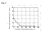
- Fig. 2 water vapor permeability
- Fig.3 oxygen permeability
- Example 1 The polyester film having an amorphous silicon layer formed thereon obtained in Example 1 was placed in a hot-air drying oven heated beforehand to 80°C, and was kept standing under those conditions for 12 hours, after which the film was taken out of the oven (Examples 4, 5 and 7).
- the polyester film having a 30 nm-thick amorphous silicon layer was thermally treated with the temperature of the hot-air drying oven set to 120°C (Example 6).
- the water vapor permeability, oxygen permeability and appearance of the films were evaluated. The results are given also in Table 1.
- Comparative Examples there were obtained a polyester film (Comparative Example 1) having no amorphous silicon layer formed thereon, and polyester films having an amorphous silicon layer formed thereon (Comparative Examples 2 and 3), using the same method as in Examples 1 through 3.
- the film thickness of the amorphous silicon layer is shown in Table 1.
- the water vapor permeability, oxygen permeability and appearance of the films were evaluated. The results are given also in Table 1.
- Table 1 Layer thickness and performance in the Examples and Comparative examples Thickness, nm, of amorphous Si layer Heat treatment at, °C Water vapor permeability, g/m 2 .24hrs. Oxygen permeability, cc/m 2 .hrs.
- the gas barrier property exhibits a superior value, but transparency decreases substantially through increased browning.
- the amorphous silicon layer thickness is preferably not larger than 200 nm in those fields where transparency is essential.
- the gas barrier plastic film of the present invention is remarkably superior as regards water vapor blocking performance and oxygen blocking performance, and is highly valuable in manufacturing fields where such properties are required.
- the gas barrier plastic film of the present invention which can be used as a packaging material for electronic components or the like that require air tightness, or as a gas barrier material for sealing against the atmosphere, has thus considerable industrial value.
Landscapes
- Chemical & Material Sciences (AREA)
- Chemical Kinetics & Catalysis (AREA)
- Organic Chemistry (AREA)
- Health & Medical Sciences (AREA)
- Medicinal Chemistry (AREA)
- Polymers & Plastics (AREA)
- General Chemical & Material Sciences (AREA)
- Engineering & Computer Science (AREA)
- Materials Engineering (AREA)
- Mechanical Engineering (AREA)
- Metallurgy (AREA)
- Inorganic Chemistry (AREA)
- Laminated Bodies (AREA)
Applications Claiming Priority (1)
| Application Number | Priority Date | Filing Date | Title |
|---|---|---|---|
| JP2006294423A JP4397391B2 (ja) | 2006-10-30 | 2006-10-30 | ガスバリア性プラスチックおよびプラスチックフィルムの製造方法 |
Publications (2)
| Publication Number | Publication Date |
|---|---|
| EP1918319A2 true EP1918319A2 (de) | 2008-05-07 |
| EP1918319A3 EP1918319A3 (de) | 2009-02-18 |
Family
ID=39092028
Family Applications (1)
| Application Number | Title | Priority Date | Filing Date |
|---|---|---|---|
| EP07119611A Withdrawn EP1918319A3 (de) | 2006-10-30 | 2007-10-30 | Gasbarrierenkunststoffkörper und -folie |
Country Status (3)
| Country | Link |
|---|---|
| US (1) | US20080102260A1 (de) |
| EP (1) | EP1918319A3 (de) |
| JP (1) | JP4397391B2 (de) |
Families Citing this family (4)
| Publication number | Priority date | Publication date | Assignee | Title |
|---|---|---|---|---|
| DE10308381B4 (de) * | 2003-02-27 | 2012-08-16 | Forschungszentrum Jülich GmbH | Verfahren zur Abscheidung von Silizium |
| KR20100088130A (ko) * | 2007-11-16 | 2010-08-06 | 오꾸라 고교 가부시키가이샤 | 태양 전지 모듈용 이면 보호 시트 및 그것으로 보호한 태양 전지 모듈 |
| JP5598080B2 (ja) | 2010-05-17 | 2014-10-01 | 大日本印刷株式会社 | ガスバリア性シートの製造方法 |
| JP2012017456A (ja) * | 2010-06-11 | 2012-01-26 | Fujifilm Corp | ポリエステルフィルム及びその製造方法、太陽電池用バックシート、並びに太陽電池モジュール |
Family Cites Families (6)
| Publication number | Priority date | Publication date | Assignee | Title |
|---|---|---|---|---|
| US4242403A (en) * | 1976-08-02 | 1980-12-30 | Libbey-Owens-Ford Company | Automotive glazing units and method of producing the same |
| CA1266591A (en) * | 1987-10-07 | 1990-03-13 | Michael R. Wertheimer | Process for modifying large polymeric surfaces |
| JPH04287314A (ja) * | 1991-03-15 | 1992-10-12 | Toyobo Co Ltd | 水素化アモルファスシリコン積層体とその製法 |
| JPH08174763A (ja) * | 1994-12-27 | 1996-07-09 | Dainippon Printing Co Ltd | 包装体 |
| US6180871B1 (en) * | 1999-06-29 | 2001-01-30 | Xoptix, Inc. | Transparent solar cell and method of fabrication |
| JP2001111076A (ja) * | 1999-10-08 | 2001-04-20 | Tdk Corp | コーティング体および太陽電池モジュール |
-
2006
- 2006-10-30 JP JP2006294423A patent/JP4397391B2/ja not_active Expired - Fee Related
-
2007
- 2007-10-29 US US11/926,804 patent/US20080102260A1/en not_active Abandoned
- 2007-10-30 EP EP07119611A patent/EP1918319A3/de not_active Withdrawn
Also Published As
| Publication number | Publication date |
|---|---|
| JP4397391B2 (ja) | 2010-01-13 |
| JP2008110522A (ja) | 2008-05-15 |
| EP1918319A3 (de) | 2009-02-18 |
| US20080102260A1 (en) | 2008-05-01 |
Similar Documents
| Publication | Publication Date | Title |
|---|---|---|
| KR100613326B1 (ko) | 산소 차단 복합 필름 구조물 | |
| CN1910040B (zh) | 阻气性膜以及阻气性叠层体 | |
| JP5889281B2 (ja) | バリア性蒸着フィルム | |
| JP5521360B2 (ja) | ガスバリアフィルムの製造方法 | |
| CN103079807A (zh) | 层叠体和层叠体的制造方法 | |
| JP2011173261A (ja) | ガスバリアフィルムおよびその製造方法 | |
| JP4994073B2 (ja) | ガスバリア積層フィルムとその製造方法。 | |
| WO2019044088A1 (ja) | 太陽電池モジュール | |
| EP1918319A2 (de) | Gasbarrierenkunststoffkörper und -folie | |
| EP2692523A1 (de) | Gasbarrierenlaminatfilm und herstellungsverfahren dafür | |
| JP2013253319A (ja) | ガスバリア性フィルム及びその製造方法 | |
| JPWO2012060424A1 (ja) | ガスバリア性積層フィルム | |
| JP2013233744A (ja) | ガスバリア性フィルム及びガスバリア性フィルムの製造方法 | |
| JP6171542B2 (ja) | ガスバリア性フィルム及びガスバリア性フィルムの製造方法 | |
| TW201247924A (en) | Method for producing laminate | |
| JP4757364B2 (ja) | 太陽電池モジュ−ル | |
| WO2013168739A1 (ja) | ガスバリア性フィルム及びその製造方法 | |
| JP2000340818A (ja) | 太陽電池モジュ−ル用保護シ−トおよびそれを使用した太陽電池モジュ−ル | |
| JP2012057237A (ja) | ガスバリアフィルムの製造方法 | |
| JP2000332275A (ja) | 太陽電池モジュ−ル用保護シ−トおよびそれを使用した太陽電池モジュ−ル | |
| JP2000332277A (ja) | 太陽電池モジュ−ル用保護シ−トおよびそれを使用した太陽電池モジュ−ル | |
| JP2013233746A (ja) | ガスバリア性フィルム及びその製造方法 | |
| JP5982904B2 (ja) | ガスバリア性積層フィルムおよびガスバリア性積層フィルムの製造方法 | |
| JP2013072120A (ja) | ガスバリアフィルムの製造方法およびガスバリアフィルム | |
| JP2009228015A (ja) | 積層体の製造方法および製造装置ならびにガスバリアフィルム |
Legal Events
| Date | Code | Title | Description |
|---|---|---|---|
| PUAI | Public reference made under article 153(3) epc to a published international application that has entered the european phase |
Free format text: ORIGINAL CODE: 0009012 |
|
| AK | Designated contracting states |
Kind code of ref document: A2 Designated state(s): AT BE BG CH CY CZ DE DK EE ES FI FR GB GR HU IE IS IT LI LT LU LV MC MT NL PL PT RO SE SI SK TR |
|
| AX | Request for extension of the european patent |
Extension state: AL BA HR MK RS |
|
| PUAL | Search report despatched |
Free format text: ORIGINAL CODE: 0009013 |
|
| AK | Designated contracting states |
Kind code of ref document: A3 Designated state(s): AT BE BG CH CY CZ DE DK EE ES FI FR GB GR HU IE IS IT LI LT LU LV MC MT NL PL PT RO SE SI SK TR |
|
| AX | Request for extension of the european patent |
Extension state: AL BA HR MK RS |
|
| AKX | Designation fees paid | ||
| STAA | Information on the status of an ep patent application or granted ep patent |
Free format text: STATUS: THE APPLICATION IS DEEMED TO BE WITHDRAWN |
|
| 18D | Application deemed to be withdrawn |
Effective date: 20090919 |
|
| REG | Reference to a national code |
Ref country code: DE Ref legal event code: 8566 |