EP1916722A2 - Karbonfilamentspeicher und Herstellungsverfahren dafür - Google Patents
Karbonfilamentspeicher und Herstellungsverfahren dafür Download PDFInfo
- Publication number
- EP1916722A2 EP1916722A2 EP07119159A EP07119159A EP1916722A2 EP 1916722 A2 EP1916722 A2 EP 1916722A2 EP 07119159 A EP07119159 A EP 07119159A EP 07119159 A EP07119159 A EP 07119159A EP 1916722 A2 EP1916722 A2 EP 1916722A2
- Authority
- EP
- European Patent Office
- Prior art keywords
- carbon
- memory
- carbon layer
- mass storage
- carbon material
- Prior art date
- Legal status (The legal status is an assumption and is not a legal conclusion. Google has not performed a legal analysis and makes no representation as to the accuracy of the status listed.)
- Granted
Links
Images




Classifications
-
- H—ELECTRICITY
- H10—SEMICONDUCTOR DEVICES; ELECTRIC SOLID-STATE DEVICES NOT OTHERWISE PROVIDED FOR
- H10N—ELECTRIC SOLID-STATE DEVICES NOT OTHERWISE PROVIDED FOR
- H10N70/00—Solid-state devices having no potential barriers, and specially adapted for rectifying, amplifying, oscillating or switching
- H10N70/801—Constructional details of multistable switching devices
- H10N70/881—Switching materials
- H10N70/884—Switching materials based on at least one element of group IIIA, IVA or VA, e.g. elemental or compound semiconductors
- H10N70/8845—Carbon or carbides
-
- H—ELECTRICITY
- H10—SEMICONDUCTOR DEVICES; ELECTRIC SOLID-STATE DEVICES NOT OTHERWISE PROVIDED FOR
- H10B—ELECTRONIC MEMORY DEVICES
- H10B63/00—Resistance change memory devices, e.g. resistive RAM [ReRAM] devices
- H10B63/30—Resistance change memory devices, e.g. resistive RAM [ReRAM] devices comprising selection components having three or more electrodes, e.g. transistors
-
- H—ELECTRICITY
- H10—SEMICONDUCTOR DEVICES; ELECTRIC SOLID-STATE DEVICES NOT OTHERWISE PROVIDED FOR
- H10N—ELECTRIC SOLID-STATE DEVICES NOT OTHERWISE PROVIDED FOR
- H10N70/00—Solid-state devices having no potential barriers, and specially adapted for rectifying, amplifying, oscillating or switching
- H10N70/011—Manufacture or treatment of multistable switching devices
- H10N70/021—Formation of switching materials, e.g. deposition of layers
- H10N70/023—Formation of switching materials, e.g. deposition of layers by chemical vapor deposition, e.g. MOCVD, ALD
-
- H—ELECTRICITY
- H10—SEMICONDUCTOR DEVICES; ELECTRIC SOLID-STATE DEVICES NOT OTHERWISE PROVIDED FOR
- H10N—ELECTRIC SOLID-STATE DEVICES NOT OTHERWISE PROVIDED FOR
- H10N70/00—Solid-state devices having no potential barriers, and specially adapted for rectifying, amplifying, oscillating or switching
- H10N70/011—Manufacture or treatment of multistable switching devices
- H10N70/021—Formation of switching materials, e.g. deposition of layers
- H10N70/026—Formation of switching materials, e.g. deposition of layers by physical vapor deposition, e.g. sputtering
-
- H—ELECTRICITY
- H10—SEMICONDUCTOR DEVICES; ELECTRIC SOLID-STATE DEVICES NOT OTHERWISE PROVIDED FOR
- H10N—ELECTRIC SOLID-STATE DEVICES NOT OTHERWISE PROVIDED FOR
- H10N70/00—Solid-state devices having no potential barriers, and specially adapted for rectifying, amplifying, oscillating or switching
- H10N70/20—Multistable switching devices, e.g. memristors
- H10N70/231—Multistable switching devices, e.g. memristors based on solid-state phase change, e.g. between amorphous and crystalline phases, Ovshinsky effect
- H10N70/235—Multistable switching devices, e.g. memristors based on solid-state phase change, e.g. between amorphous and crystalline phases, Ovshinsky effect between different crystalline phases, e.g. cubic and hexagonal
-
- H—ELECTRICITY
- H10—SEMICONDUCTOR DEVICES; ELECTRIC SOLID-STATE DEVICES NOT OTHERWISE PROVIDED FOR
- H10N—ELECTRIC SOLID-STATE DEVICES NOT OTHERWISE PROVIDED FOR
- H10N70/00—Solid-state devices having no potential barriers, and specially adapted for rectifying, amplifying, oscillating or switching
- H10N70/801—Constructional details of multistable switching devices
- H10N70/821—Device geometry
- H10N70/826—Device geometry adapted for essentially vertical current flow, e.g. sandwich or pillar type devices
-
- G—PHYSICS
- G11—INFORMATION STORAGE
- G11C—STATIC STORES
- G11C2213/00—Indexing scheme relating to G11C13/00 for features not covered by this group
- G11C2213/30—Resistive cell, memory material aspects
- G11C2213/35—Material including carbon, e.g. graphite, grapheme
-
- Y—GENERAL TAGGING OF NEW TECHNOLOGICAL DEVELOPMENTS; GENERAL TAGGING OF CROSS-SECTIONAL TECHNOLOGIES SPANNING OVER SEVERAL SECTIONS OF THE IPC; TECHNICAL SUBJECTS COVERED BY FORMER USPC CROSS-REFERENCE ART COLLECTIONS [XRACs] AND DIGESTS
- Y10—TECHNICAL SUBJECTS COVERED BY FORMER USPC
- Y10T—TECHNICAL SUBJECTS COVERED BY FORMER US CLASSIFICATION
- Y10T428/00—Stock material or miscellaneous articles
- Y10T428/30—Self-sustaining carbon mass or layer with impregnant or other layer
Definitions
- the present invention relates generally to memories and in one embodiment to a carbon filament memory.
- Nonvolatile memory retains its stored data even when power is not present.
- This type of memory is used in a wide variety of electronic equipment, including digital cameras, portable audio players, wireless communication devices, personal digital assistants, and peripheral devices, as well as for storing firmware in computers and other devices.
- Nonvolatile memory technologies include flash memory, magnetoresistive random access memory (MRAM), phase change random access memory (PCRAM), and conductive bridging random access memory (CBRAM). Due to the great demand for nonvolatile memory devices, researchers are continually developing new types of nonvolatile memory.
- MRAM magnetoresistive random access memory
- PCRAM phase change random access memory
- CBRAM conductive bridging random access memory
- the invention provides an integrated circuit including a memory element including a first carbon layer rich in a first carbon material and a second carbon layer rich in a second carbon material.
- the memory element stores information by reversibly forming a conductive channel in the second carbon layer, wherein the conductive channel includes the first carbon material.
- FIGS. 1A and 1B show a conventional conductive bridging memory element
- FIGS. 2A, 2B, and 2C show a carbon filament memory element in accordance with an embodiment of the invention
- FIG 3 is a graph showing different resistances in a carbon filament memory element in accordance with an embodiment of the invention.
- FIG. 4 is a graph showing V-I curves that demonstrate the memory effect of a carbon filament memory element in accordance with an embodiment of the invention
- FIG. 5 is a block diagram of a method for storing information in accordance with an embodiment of the invention.
- FIG. 6 is a schematic diagram of a memory cell in accordance with an embodiment of the invention.
- FIG. 7 is a block diagram showing a method for manufacturing an array of memory cells in accordance with an embodiment of the invention.
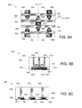
- FIGS. 8A, 8B, and 8C show a top view and cross section views of a memory array in accordance with an embodiment of the invention, following an intermediate step in the manufacture of the memory array;
- FIGS. 9A and 9B show a top view and a cross section view of a memory array in accordance with an embodiment of the invention, following another step in the manufacture of the memory array;
- FIG. 10 shows an example computing system including a memory device using memory cells in accordance with an embodiment of the invention
- FIGS. 11A and 11B show a memory module and a stackable memory module, respectively, using memory cells in accordance with an embodiment of the invention
- FIG. 12 shows a system that emulates a mass storage device using a non-volatile memory device according to an embodiment of the invention.
- FIG. 13 shows a block diagram of a hybrid mass storage device that stores data to a mass storage device or to a non-volatile memory device according to an embodiment of the invention.
- FIG. 1A shows a conventional conductive bridging junction (CBJ) for use in a conductive bridging random access memory (CBRAM) cell.
- a CBJ 100 includes a first electrode 102, a second electrode 104, and a solid electrolyte block 106 sandwiched between the first electrode 102 and the second electrode 104.
- the first electrode 102 contacts a first surface 108 of the solid electrolyte block 106
- the second electrode 104 contacts a second surface 110 of the solid electrolyte block 106.
- One of the first electrode 102 and the second electrode 104 is a reactive electrode, the other one an inert electrode.
- the first electrode 102 is the reactive electrode
- the second electrode 104 is the inert electrode.
- the first electrode 102 includes silver (Ag)
- the solid electrolyte block 106 includes a silver-doped chalcogenide material.
- a sensing current is routed through the CBJ 100.
- the sensing current encounters a high resistance if no conductive bridge 114 exists within the CBJ 100, and a low resistance when a conductive bridge 114 is present.
- a high resistance may, for example, represent "0", while a low resistance represents "1", or vice versa.
- a process of forming a reversible conductive filament may be used to construct an information storage element using a carbon layer system including layers of sp 2 -rich and sp 3 -rich (also known as diamond-like carbon, or DLC) amorphous carbon films.
- a carbon layer system including layers of sp 2 -rich and sp 3 -rich (also known as diamond-like carbon, or DLC) amorphous carbon films.
- a memory junction 200 includes a top contact 202, a first carbon layer 204 including an amorphous carbon material rich in sp 2 hybridized carbon atoms, a second carbon layer 206 including an amorphous carbon material rich in sp 3 hybridized carbon atoms, and a bottom contact 208.
- the first carbon layer 204 and second carbon layer 206 form a carbon bi-layer system 210 in which a conductive filament may be formed, as described further below.
- the sp 2 -rich carbon is conductive
- the sp 3 -rich carbon is an electrical insulator, having low conductivity.
- the resistance of the first carbon layer 204 i.e., the sp 2 -rich carbon layer
- the resistance of the second carbon layer 206 is R2
- the ratio R2/R1 may be greater than 100, for example greater than 1000, e.g., greater than 10000.
- an sp 2 filament 250 can be formed in the sp 3 -rich second carbon layer 206, changing the conductivity (and resistance) of the carbon bi-layer system.
- the current causes a change in the structure of the material, from atomic scale sp 2 /sp 3 disorder to a disordered graphitic sp 2 -domain network, through the migration of sp 3 defects.
- the current induces the migration of sp 2 -rich clusters to form a percolation path network of graphitic sp 2 domains, which causes an insulator-to-metal transition.
- Electron transport in the sp 2 -rich metallic state features weakly temperature-dependent conductivity with a majority of hole and a minority of electron carriers.
- a one-dimensional channel arises due to filamentary conduction through localized sp 2 -rich regions within the sp 3 carbon barriers, and particularly within the barrier adjacent to the electron injector. This limits the electrical conduction at low bias. Additionally, this may involve the orientation of ⁇ orbitals of sp 2 -bonded carbon molecules when subject to a high electric field, leading to increased electron transmission, although the present invention is not limited to a particular theory of operation.
- the thickness of the sp 3 -rich second carbon layer 206 is related to the desired voltages and speed for the operation of the memory. Switching (i.e., formation or removal of filaments) may occur in an electric field of less than one volt per nm of thickness of the material. For example, for an operating voltage of 3V, the thickness of the second carbon layer 206 may be approximately 4 nm.
- the thickness of the sp 2 -rich first carbon layer 204 does not have a substantial effect, and the first carbon layer 204 may have almost any thickness, from a monolayer to a thickness of hundreds of nm.
- FIG. 3 shows a curve 300 representing the resistance in an 8 nm thick sp 3 -rich film, as voltage varies.
- the curve 300 includes quantized resistance steps 302a-302e, in multiples of hl (2 e 2 ), where h is Planck's constant and e is the electron charge, indicating the formation of additional conducting channels in the sp 3 -rich carbon film.
- FIG. 4 illustrates the memory effect following the application of voltage to an sp 3 -rich film.
- the I-V curve 400 shows the current/voltage relationship for an approximately 8 nm thick sp 3 -rich film prior to the formation of carbon filaments in the sp 3 -rich film.
- the I-V curve 402 shows the current/voltage relationship after formation of filaments using a voltage pulse of approximately 6 volts, demonstrating the memory effect.
- FIG. 5 shows a block diagram of a method for storing information according to an embodiment of the invention.
- a carbon bi-layer system as described above, including an sp 2 -rich amorphous carbon layer and an sp 3 -rich amorphous carbon layer is provided.
- information is stored in the carbon bi-layer system by applying a current through the carbon bi-layer system to cause the growth of a filament of sp 2 -rich carbon in the sp 3 -rich layer, decreasing the resistance of the carbon bi-layer system. By applying a current with reversed polarity, the growth of the filament can be reversed. Additionally, quantized resistance steps, such as are shown in FIG. 3, can be used to store multiple bits of information in the carbon bi-layer system.
- FIG. 6 shows an illustrative memory cell that uses a memory junction such as is shown in FIGS. 2A-2C, with still others being apparent to workers in the art and included herein.
- the memory cell 600 includes a select transistor 602 and a memory junction 604, which uses a carbon bi-layer system, in accordance with the invention.
- the select transistor 602 includes a source 606 that is connected to a bit line 608, a drain 610 that is connected to the memory junction 604, and a gate 612 that is connected to a word line 614.
- the memory junction 604 is also connected to a common line 616, which may be connected to ground, or to other circuitry, such as circuitry (not shown) for determining the resistance of the memory cell 600, for use in reading.
- the terms connected and coupled are intended to include both direct and indirect connection and coupling, respectively.
- the word line 614 is used to select the cell 600, and a current on the bit line 608 is forced through the memory junction 604, to form or remove filaments in the memory junction 604, changing the resistance of the memory junction 604.
- the word line 614 is used to select the cell 600, and the bit line 608 is used to apply a voltage across the memory junction 604 to measure the resistance of the memory junction 604.
- the memory cell 600 may be referred to as a 1T1J cell, because it uses one transistor, and one memory junction.
- a memory device will include an array of many such cells. It will be understood that other configurations for a 1T1J memory cell could be used with a carbon bi-layer memory junction according to the invention. Additionally, cell configurations other than a 1T1J configuration may be used.
- an illustrative method for manufacturing an integrated circuit including an array of 1T1J memory cells that have a memory junction using a carbon layer system in accordance with an embodiment of the invention is described.
- the manufacturing may be accomplished by any method known in the art or hereafter developed that is suitable for forming the inventive structure.
- a shallow trench isolation (STI) structure in the array and periphery has been manufactured on a semiconductor wafer or other suitable substrate.
- STI shallow trench isolation
- gates and word lines are formed above the STI structure. This involves the conventional application of a gate oxide layer, gate conductor deposition and structuring, sidewall spacer formation, and related implants.
- SiO 2 is removed from the source and drain regions. This may be accomplished, for example, through the application of diluted HF. Optionally, selective epitaxial growth of Si may be used to form elevated source and drain regions.
- step 706 by a salicidation process, for example forming CoSi, NiSi, TiSi, or another suitable silicide.
- Salicidation can be omitted in parts or all of the periphery by using a blocking mask.
- salicided areas where no contacts will be manufactured may be covered with resist.
- Step 708 is an ILD (Interlayer Dielectric) deposition step which can be, for example, an SiO 2 deposition and planarization step, which is followed in step 710 by etching contact holes (vias) and filling them with contact plugs including a suitable conductive material, such as W, poly-Si, or a conductive carbon material. Back etching and planarization may be used to prepare a level surface for the wafer.
- ILD Interlayer Dielectric
- bit lines are formed, which are connected to the common source of two neighboring transistors. This may be achieved by using a lithographic process to mask portions of the SiO 2 layer, etching the SiO 2 and the common source contact plug for formation of the bit lines. This is followed by deposition of the bit lines (using poly-Si, W, or other suitable conductive materials) and recess.
- step 714 further (ILD) SiO 2 is deposited, burying the bit lines.
- CMP Chemical mechanical polishing
- the sp 3 -rich and sp 2 -rich carbon layers are deposited to form the carbon bi-layer system for the memory junction.
- Deposition of these layers may be achieved by physical vapor deposition (PVD), chemical vapor deposition (CVD), plasma enhanced chemical vapor deposition (PECVD), ablation of a graphite target using a 248 nm pulsed ultraviolet excimer laser, or another suitable method of depositing a material on a substrate.
- the sp 2 to sp 3 ratio in the deposited carbon materials may be varied by a number of methods, depending on the deposition technique used. For example, if the carbon layers are produced using PECVD deposition, the ratio may be controlled by adjusting the bias voltage, gas pressure, and temperature during the deposition of the material.
- the PECVD process may be carried out in an inductively coupled high-density plasma with a stimulation frequency of approximately 20 MHz to approximately 40 MHz, e.g., with a stimulation frequency of approximately 25 MHz to approximately 30 MHz, e.g., with a stimulation frequency of approximately 27.26 MHz.
- the substrate including the layer stack that has already been manufactured, is placed on a substrate holder where it is possible to apply an RF bias voltage. Additional ions having the appropriate energy can be pulled onto the substrate by means of the RF bias voltage. Additionally, the substrate can be heated.
- C x H y (x and y are arbitrary natural number), e.g., C 2 H 2 or CH 4 , can be used as the reactive gas.
- the reactive gas can be diluted using Ne, H 2 or Ar.
- the level of the substrate bias voltage is determined by the reactor geometry (i.e. the ratio of the dimensions of the mass carrying electrode and the RF carrying electrode in the reactor), and by the self-bias, which is applied or is adjusted to by an externally applied capacitively coupled-in RF field.
- the externally applied capacitively coupled-in RF field determines the layer characteristics and, for example, the occurring bondings, such as sp 3 or sp 2 bondings, and their relative amount and mixture.
- a negative voltage in the range of approximately 50 V to approximately 350 V is applied together with a gas pressure in the range of approximately 10 mTorr to approximately 500 mTorr.
- a small voltage of, e.g., 50 V may be applied and for a highly conductive layer a voltage of, e.g., 300 V may be applied.
- the ratio of sp 2 to sp 3 may be determined by forming the layers by sputtering. This may be achieved, for example, using a graphite target in an argon atmosphere, at a pressure of approximately 1 Pa, with the substrate approximately 3 cm from the target.
- the temperature in a range of approximately 77 K to 500 K, and the sputtering power from approximately 5 W to approximately 300 W, the resistivity of the material may be varied. For a low conductivity layer a small power of, e.g., 5 W may be applied and for a highly conductive layer a power of, e.g., 300 W may be applied.
- the ratio of sp 2 to sp 3 may be determined by forming the layers by laser ablation.
- a 248 nm pulsed ultraviolet excimer laser e.g., Lambda Physik LPX 210i
- the fluence of the laser may be varied to synthesize two types of amorphous-carbon layers (using, for example, approximately 4 J cm -2 for sp2-rich layers and approximately 20 J cm -2 for sp3-rich layers).
- the amounts of sp 2 and sp 3 hybridized carbon present in a deposited film may also be adjusted by post-deposition annealing, or by other conventional techniques for depositing films of diamond-like carbon.
- the top electrode including a highly conductive material such as poly-Si, W, Ti, or Ta is deposited above the carbon bi-layer system.
- step 720 lithography and etching are used to define the areas covered by the carbon bi-layer system and top electrode. Following this step, additional processing of the semiconductor wafer may be performed using conventional processes.
- FIGS. 8A-8C illustrate one intermediate step in the above-described process.
- they show a portion of the integrated circuit following step 710, in which the contact holes are etched and filled with a material such as W, poly-Si, or carbon.
- FIG. 8A shows a top view of a portion of a memory array 800, including active areas 802, word lines 804, and filled contact holes 806.
- the density of memory cells in an array may be increased by sharing each active area 802 (in this case, sharing a source region) between two cells, each with its own word line.
- the staggered arrangement of the active areas 802 also contributes to increasing the density of memory cells in the array. It will be understood that other layouts of memory cells and active areas may also be used, and that the layout shown in FIGS. 8A-8C is for the purpose of illustration.
- FIG. 8B shows a cross section of the portion of the memory array 800 along Cut A-A of FIG. 8A.
- This cross section shows one active area 802, and two word lines 804, connected to transistor gates 820.
- Filled contact holes 806 have been etched through an SiO 2 layer 822 to connect to a source contact area 824, and to two drain contact areas 826.
- the active areas 802 are separated by STI areas 828.
- FIG. 8C shows a second cross section of the portion of the memory array 800 along Cut B-B of FIG. 8A. This cross section shows portions of three active areas 802, separated by STI areas 828. Filled contact holes 806, etched through the SiO 2 layer 822 connect to drain contact areas 826.
- FIGS. 9A and 9B show a similar view, following step 720 of the method 700, described above with reference to FIG. 7.
- FIG. 9A is a top view, showing the portion of a memory array 900, which is the same as the portion of the memory array 800 described with reference to FIGS. 8A-8C, but at a later stage in processing.
- the portion of the memory array 900 now includes top electrodes 902, which are deposited above carbon bi-layer memory junctions.
- FIG. 9B shows a cross section of the portion of the memory array 900 along Cut A-A, which is similar in location to the cross section shown above in FIG. 8B.
- the cross section shows an active area 920, and two word lines 922, connected to transistor gates 924.
- Vias (or contact plugs) 926 connect to two drain contact areas 928, and to carbon bi-layer memory junctions 930, which are connected to top electrodes 902.
- a bit line 932 connects to a source contact region 934 through a via 936.
- STI areas 938 separate the active area 920 from other active areas.
- bit line 932, via 936, and source contact region 934 are shared by two memory cells, each of which includes a transistor and a carbon bi-layer memory junction 930. It will be understood that other layouts for memory cells may be used in accordance with the principles of the invention.
- Memory cells such as are described above may be used in memory devices that contain large numbers of such cells. These cells may, for example, be organized into an array of memory cells having numerous rows and columns of cells, each of which stores one or more bits of information. Memory devices of this sort may be used in a variety of applications or systems, such as the illustrative system shown in FIG. 10.
- FIG. 10 shows an example computing system that uses a memory device constructed of memory cells in accordance with the invention.
- the computing system 1000 includes a memory device 1002, which may utilize memory cells in accordance with the invention.
- the system also includes a processor 1004, and one or more input/output devices, such as a keypad 1006, display 1008, and wireless communication device 1010.
- the memory device 1002, processor 1004, keypad 1006, display 1008 and wireless communication device 1010 are interconnected by a bus 1012.
- the wireless communication device 1010 may include circuitry (not shown) for sending and receiving transmissions over a cellular telephone network, a WiFi wireless network, or other wireless communication network. It will be understood that the variety of input/output devices shown in FIG. 10 is merely an example, in which the computing system 1000 may be configured as a cellular telephone or other wireless communications device. Memory devices including memory cells in accordance with the invention may be used in a wide variety of systems. Alternative system designs may include different input/output devices, multiple processors, alternative bus configurations, and many other configurations.
- memory cells such as those described above may be used in modules.
- a memory module 1100 is shown, on which one or more memory devices 1104 are arranged on a substrate 1102.
- the memory device 1104 may include numerous memory cells, each of which uses a memory element as described above.
- the memory module 1100 may also include one or more electronic devices 1106, which may include memory, processing circuitry, control circuitry, addressing circuitry, bus interconnection circuitry, or other circuitry or electronic devices that may be combined on a module with a memory device, such as the memory device 1104.
- the memory module 1100 includes multiple electrical connections 1108, which may be used to connect the memory module 1100 to other electronic components, including other modules.
- these modules may be stackable, to form a stack 1150.
- a stackable memory module 1152 may contain one or more memory devices 1156, arranged on a stackable substrate 1154.
- the memory device 1156 contains memory cells that employ memory elements such as are described above.
- the stackable memory module 1152 may also include one or more electronic devices 1158, which may include memory, processing circuitry, control circuitry, addressing circuitry, bus interconnection circuitry, or other circuitry or electronic devices that may be combined on a module with a memory device, such as the memory device 1156.
- Electrical connections 1160 are used to connect the stackable memory module 1152 with other modules in the stack 1150, or with other electronic devices.
- Other modules in the stack 1150 may include additional stackable memory modules, similar to the stackable memory module 1152 described above, or other types of stackable modules, such as stackable processing modules, control modules, communication modules, or other modules containing electronic components.
- FIG. 12 shows a system 1200, in which a non-volatile memory 1202 according to an embodiment of the invention is used to emulate a hard drive or other mass storage device. Because the non-volatile memory 1202 has a faster access time than a typical hard drive, by storing commonly-used software and data on the non-volatile memory device, the performance of the system may be improved.
- the system 1200 includes a system memory 1204, a system processor 1206, and an integrated circuit package 1208.
- the integrated circuit package 1208 includes the non-volatile memory 1202, and a controller 1210.
- a system bus 1212 interconnects the system memory 1204, the system processor 1206, and the integrated circuit package 1208. It will be understood that a variety of other devices (not shown) may also be interconnected on the system bus 1212, such as a variety of input/output devices (not shown), additional processors (not shown), or other devices suitable for use with a computing system.
- the non-volatile memory 1202 includes memory cells in accordance with an embodiment of the invention, as described above.
- the non-volatile memory 1202 is connected to the controller 1210, which interfaces the non-volatile memory 1202 to the system bus 1212.
- the controller 1210 may emulate the interface of a hard disk or other mass storage device.
- the system memory 1204 may include conventional memory, such as conventional DRAM, or may include memory cells in accordance with the invention, as described above.
- the non-volatile memory 1202 may be used to improve the performance and reliability of the system 1200 by storing commonly used applications and data.
- the non-volatile memory 1202 may store components of an operating system.
- the non-volatile memory 1202 may store software for emulating a hard disk or other mass storage device.
- the controller 1210 may include the ability to intercept a system boot process (such as a BIOS boot process on some computer systems), and install the software for emulating a hard disk from the non-volatile memory 1202 to the system memory 1204.
- the non-volatile memory 1202 may be arranged so that it is accessed in a block-oriented manner, providing access to blocks of data, similar to the block-oriented manner in which data are arranged on a conventional hard disk drive.
- the size of a block of data will depend on the amount of storage in the non-volatile memory, and typically ranges from 512 bytes to 64 kilobytes or more, though other block sizes may also be used.
- FIG. 12 is an example, and that many other system configurations may be used in accordance with embodiments of the invention.
- Alternative system configurations may include a variety input/output devices, multiple processors, alternative bus configurations, and many other configurations of a computing system.
- the components shown in FIG. 12 may be separate, or may be integrated into a single device or module, or into multiple devices and modules.
- the system processor 1206 may be integrated into a single device with the system memory 1204 and one or more input/output devices.
- a system such as is shown in FIG. 12 may be configured for general use, or for special purposes, such as cellular or wireless communication, photography, playing music or other digital media, or other purposes.
- a memory such as is described above may be used in hybrid mass storage device, such as a hybrid hard disk drive, as shown in FIG. 13.
- the hybrid drive 1300 shown in FIG. 13 includes a non-volatile memory 1302 that includes memory cells in accordance with an embodiment of the invention, as described above. Additionally, the hybrid drive 1300 includes a second mass storage medium 1304, such as a conventional magnetic hard disk or an optical disk, and a controller 1306.
- the controller 1306 is connected to the non-volatile memory 1302 and to the second mass storage medium 1304, and routes requests to access data storage to either the non-volatile memory 1302, the second mass storage medium 1304, or to both.
- the controller 1306 may be combined with a mass storage device controller, such as a hard disk drive controller or an optical drive controller, and may handle the functions of a conventional mass storage device controller in addition to routing access requests to the non-volatile memory 1302 or the second mass storage medium 1304.
- a mass storage device controller such as a hard disk drive controller or an optical drive controller
- the hybrid drive 1300 is used in the same manner as a conventional hard disk drive, and generally will have the same appearance, dimensions, and interface as a conventional disk drive device or other mass storage device. However, because the non-volatile memory 1302 typically has a faster access time than the second mass storage medium 1304, and typically requires less power, the hybrid drive 1300 may achieve higher performance and lower power use than a conventional hard disk drive, by storing a portion of the data, such as frequently used data, in the non-volatile memory, rather than on the second mass storage medium.
- Blocks of data on the hybrid drive 1300 may be accessed according to a block address, in a manner similar to those used with a conventional hard disk drive or other mass storage device. Based on the address, the controller 1306 may direct the request to the non-volatile memory 1302 or to the second mass storage medium 1304. In some embodiments, this is accomplished using an address mapping to determine how to direct access requests. This mapping may be stored in a table or other data structure that is used by the controller 1306 to route the access requests. Since most conventional mass storage devices access data in a block-oriented manner, in some embodiments, the non-volatile memory 1302 may be organized in a block-oriented manner, with block sizes typically ranging from 512 bytes to 64 kilobytes or more, though other block sizes are possible. Typically, the block size used for the non-volatile memory 1302 will be the same as the block size used for the second mass storage medium, though differing block sizes are possible, and may be used in some embodiments.
- a hybrid drive including a non-volatile memory may be used in accordance with an embodiment of the invention.
- a hybrid drive may include additional mass storage devices, additional memory for use as a cache, or other configurations.
Landscapes
- Chemical & Material Sciences (AREA)
- Crystallography & Structural Chemistry (AREA)
- Engineering & Computer Science (AREA)
- Manufacturing & Machinery (AREA)
- Semiconductor Memories (AREA)
Applications Claiming Priority (2)
| Application Number | Priority Date | Filing Date | Title |
|---|---|---|---|
| US11/588,864 US20080102278A1 (en) | 2006-10-27 | 2006-10-27 | Carbon filament memory and method for fabrication |
| US11/708,757 US7894253B2 (en) | 2006-10-27 | 2007-02-20 | Carbon filament memory and fabrication method |
Publications (3)
| Publication Number | Publication Date |
|---|---|
| EP1916722A2 true EP1916722A2 (de) | 2008-04-30 |
| EP1916722A3 EP1916722A3 (de) | 2011-01-19 |
| EP1916722B1 EP1916722B1 (de) | 2012-01-18 |
Family
ID=39330568
Family Applications (1)
| Application Number | Title | Priority Date | Filing Date |
|---|---|---|---|
| EP07119159A Not-in-force EP1916722B1 (de) | 2006-10-27 | 2007-10-24 | Karbonfilamentspeicher und Herstellungsverfahren dafür |
Country Status (6)
| Country | Link |
|---|---|
| US (2) | US20080102278A1 (de) |
| EP (1) | EP1916722B1 (de) |
| JP (1) | JP2008153624A (de) |
| KR (1) | KR100922020B1 (de) |
| CN (1) | CN101170159B (de) |
| DE (1) | DE102007013595A1 (de) |
Cited By (13)
| Publication number | Priority date | Publication date | Assignee | Title |
|---|---|---|---|---|
| WO2009064842A1 (en) * | 2007-11-13 | 2009-05-22 | William Marsh Rice Unvirsity | Vertically-stacked electronic devices having conductive carbon films |
| WO2009140305A1 (en) * | 2008-05-12 | 2009-11-19 | Symetrix Corporation | Correlated electron material and process for making |
| WO2009140596A1 (en) * | 2008-05-16 | 2009-11-19 | Sandisk 3D, Llc | Carbon nano-film reversible resistance-switchable elements and methods of forming the same |
| WO2010005854A1 (en) * | 2008-07-08 | 2010-01-14 | Sandisk 3D, Llc | Carbon-based interface layer for a memory device and methods of forming the same |
| WO2010017428A1 (en) * | 2008-08-07 | 2010-02-11 | Sandisk 3D, Llc | A memory cell that includes a carbon -based memory element and methods of forming the same |
| WO2010078467A1 (en) * | 2008-12-31 | 2010-07-08 | Sandisk 3D, Llc | Modulation of resistivity in carbon-based read-writeable materials |
| US8110476B2 (en) | 2008-04-11 | 2012-02-07 | Sandisk 3D Llc | Memory cell that includes a carbon-based memory element and methods of forming the same |
| US8183121B2 (en) | 2009-03-31 | 2012-05-22 | Sandisk 3D Llc | Carbon-based films, and methods of forming the same, having dielectric filler material and exhibiting reduced thermal resistance |
| US8237146B2 (en) | 2010-02-24 | 2012-08-07 | Sandisk 3D Llc | Memory cell with silicon-containing carbon switching layer and methods for forming the same |
| US8421050B2 (en) | 2008-10-30 | 2013-04-16 | Sandisk 3D Llc | Electronic devices including carbon nano-tube films having carbon-based liners, and methods of forming the same |
| US8481396B2 (en) | 2009-10-23 | 2013-07-09 | Sandisk 3D Llc | Memory cell that includes a carbon-based reversible resistance switching element compatible with a steering element, and methods of forming the same |
| US8835892B2 (en) | 2008-10-30 | 2014-09-16 | Sandisk 3D Llc | Electronic devices including carbon nano-tube films having boron nitride-based liners, and methods of forming the same |
| US9287356B2 (en) | 2005-05-09 | 2016-03-15 | Nantero Inc. | Nonvolatile nanotube diodes and nonvolatile nanotube blocks and systems using same and methods of making same |
Families Citing this family (51)
| Publication number | Priority date | Publication date | Assignee | Title |
|---|---|---|---|---|
| US8183665B2 (en) | 2005-11-15 | 2012-05-22 | Nantero Inc. | Nonvolatile nanotube diodes and nonvolatile nanotube blocks and systems using same and methods of making same |
| US8030637B2 (en) * | 2006-08-25 | 2011-10-04 | Qimonda Ag | Memory element using reversible switching between SP2 and SP3 hybridized carbon |
| US20080102278A1 (en) * | 2006-10-27 | 2008-05-01 | Franz Kreupl | Carbon filament memory and method for fabrication |
| US7915603B2 (en) * | 2006-10-27 | 2011-03-29 | Qimonda Ag | Modifiable gate stack memory element |
| US7768812B2 (en) | 2008-01-15 | 2010-08-03 | Micron Technology, Inc. | Memory cells, memory cell programming methods, memory cell reading methods, memory cell operating methods, and memory devices |
| US8034655B2 (en) | 2008-04-08 | 2011-10-11 | Micron Technology, Inc. | Non-volatile resistive oxide memory cells, non-volatile resistive oxide memory arrays, and methods of forming non-volatile resistive oxide memory cells and memory arrays |
| US8211743B2 (en) | 2008-05-02 | 2012-07-03 | Micron Technology, Inc. | Methods of forming non-volatile memory cells having multi-resistive state material between conductive electrodes |
| US8134137B2 (en) | 2008-06-18 | 2012-03-13 | Micron Technology, Inc. | Memory device constructions, memory cell forming methods, and semiconductor construction forming methods |
| US9343665B2 (en) | 2008-07-02 | 2016-05-17 | Micron Technology, Inc. | Methods of forming a non-volatile resistive oxide memory cell and methods of forming a non-volatile resistive oxide memory array |
| WO2010029634A1 (ja) * | 2008-09-11 | 2010-03-18 | 株式会社 東芝 | 抵抗変化素子及び情報記録再生装置 |
| CN102265400A (zh) * | 2008-10-23 | 2011-11-30 | 桑迪士克3D有限责任公司 | 展示减少的分层的基于碳的存储器元件和形成其的方法 |
| US20100108976A1 (en) * | 2008-10-30 | 2010-05-06 | Sandisk 3D Llc | Electronic devices including carbon-based films, and methods of forming such devices |
| US8551855B2 (en) | 2009-10-23 | 2013-10-08 | Sandisk 3D Llc | Memory cell that includes a carbon-based reversible resistance switching element compatible with a steering element, and methods of forming the same |
| JP2011135050A (ja) | 2009-11-30 | 2011-07-07 | Toshiba Corp | 不揮発性半導体記憶装置 |
| US8551850B2 (en) | 2009-12-07 | 2013-10-08 | Sandisk 3D Llc | Methods of forming a reversible resistance-switching metal-insulator-metal structure |
| US8222704B2 (en) * | 2009-12-31 | 2012-07-17 | Nantero, Inc. | Compact electrical switching devices with nanotube elements, and methods of making same |
| US8389375B2 (en) | 2010-02-11 | 2013-03-05 | Sandisk 3D Llc | Memory cell formed using a recess and methods for forming the same |
| US8294132B2 (en) | 2010-03-30 | 2012-10-23 | Hewlett-Packard Development Company, L.P. | Graphene memristor having modulated graphene interlayer conduction |
| US8471360B2 (en) | 2010-04-14 | 2013-06-25 | Sandisk 3D Llc | Memory cell with carbon switching material having a reduced cross-sectional area and methods for forming the same |
| US8427859B2 (en) | 2010-04-22 | 2013-04-23 | Micron Technology, Inc. | Arrays of vertically stacked tiers of non-volatile cross point memory cells, methods of forming arrays of vertically stacked tiers of non-volatile cross point memory cells, and methods of reading a data value stored by an array of vertically stacked tiers of non-volatile cross point memory cells |
| US8411477B2 (en) | 2010-04-22 | 2013-04-02 | Micron Technology, Inc. | Arrays of vertically stacked tiers of non-volatile cross point memory cells, methods of forming arrays of vertically stacked tiers of non-volatile cross point memory cells, and methods of reading a data value stored by an array of vertically stacked tiers of non-volatile cross point memory cells |
| US8289763B2 (en) | 2010-06-07 | 2012-10-16 | Micron Technology, Inc. | Memory arrays |
| US8395927B2 (en) | 2010-06-18 | 2013-03-12 | Sandisk 3D Llc | Memory cell with resistance-switching layers including breakdown layer |
| US8520425B2 (en) | 2010-06-18 | 2013-08-27 | Sandisk 3D Llc | Resistive random access memory with low current operation |
| US20120043518A1 (en) * | 2010-08-18 | 2012-02-23 | Applied Materials, Inc. | Variable resistance memory element and fabrication methods |
| US8351242B2 (en) | 2010-09-29 | 2013-01-08 | Micron Technology, Inc. | Electronic devices, memory devices and memory arrays |
| US8759809B2 (en) | 2010-10-21 | 2014-06-24 | Micron Technology, Inc. | Integrated circuitry comprising nonvolatile memory cells having platelike electrode and ion conductive material layer |
| US8526213B2 (en) | 2010-11-01 | 2013-09-03 | Micron Technology, Inc. | Memory cells, methods of programming memory cells, and methods of forming memory cells |
| US8796661B2 (en) | 2010-11-01 | 2014-08-05 | Micron Technology, Inc. | Nonvolatile memory cells and methods of forming nonvolatile memory cell |
| US9454997B2 (en) | 2010-12-02 | 2016-09-27 | Micron Technology, Inc. | Array of nonvolatile memory cells having at least five memory cells per unit cell, having a plurality of the unit cells which individually comprise three elevational regions of programmable material, and/or having a continuous volume having a combination of a plurality of vertically oriented memory cells and a plurality of horizontally oriented memory cells; array of vertically stacked tiers of nonvolatile memory cells |
| US8431458B2 (en) | 2010-12-27 | 2013-04-30 | Micron Technology, Inc. | Methods of forming a nonvolatile memory cell and methods of forming an array of nonvolatile memory cells |
| US8791447B2 (en) | 2011-01-20 | 2014-07-29 | Micron Technology, Inc. | Arrays of nonvolatile memory cells and methods of forming arrays of nonvolatile memory cells |
| US8488365B2 (en) | 2011-02-24 | 2013-07-16 | Micron Technology, Inc. | Memory cells |
| US8537592B2 (en) | 2011-04-15 | 2013-09-17 | Micron Technology, Inc. | Arrays of nonvolatile memory cells and methods of forming arrays of nonvolatile memory cells |
| US8361813B1 (en) * | 2011-12-09 | 2013-01-29 | Intermolecular, Inc. | Method for generating graphene structures |
| CN104412372B (zh) * | 2012-06-29 | 2018-01-26 | 索尼公司 | 半导体装置、半导体装置的制造方法和电子设备 |
| TWI511142B (zh) * | 2012-07-30 | 2015-12-01 | Macronix Int Co Ltd | 記憶裝置的操作方法與記憶體陣列及其操作方法 |
| JP5838353B2 (ja) | 2013-03-18 | 2016-01-06 | パナソニックIpマネジメント株式会社 | 抵抗変化素子の評価方法、評価装置、検査装置、及び不揮発性記憶装置 |
| JP2015018591A (ja) | 2013-07-12 | 2015-01-29 | 株式会社東芝 | 不揮発性半導体記憶装置 |
| US9196361B2 (en) | 2013-11-21 | 2015-11-24 | Macronix International Co., Ltd. | Memory structure and operation method therefor |
| US9529657B2 (en) | 2014-02-07 | 2016-12-27 | Oracle International Corporation | Techniques for generating diagnostic identifiers to trace events and identifying related diagnostic information |
| US9529658B2 (en) * | 2014-02-07 | 2016-12-27 | Oracle International Corporation | Techniques for generating diagnostic identifiers to trace request messages and identifying related diagnostic information |
| CN104617092B (zh) * | 2014-11-06 | 2018-06-22 | 苏州捷芯威半导体有限公司 | 一种半导体器件及其制作方法 |
| US9640759B1 (en) | 2015-11-25 | 2017-05-02 | International Business Machines Corporation | Amorphous carbon resistive memory element with lateral heat dissipating structure |
| JP6871943B2 (ja) | 2016-03-28 | 2021-05-19 | オラクル・インターナショナル・コーポレイション | モバイルクラウドサービスのための予め形成された命令 |
| US20190181337A1 (en) * | 2016-09-25 | 2019-06-13 | Intel Corporation | Barriers for metal filament memory devices |
| KR102411184B1 (ko) * | 2017-10-20 | 2022-06-21 | 에스케이하이닉스 주식회사 | 저항 변화 메모리 소자 |
| US10460444B2 (en) * | 2018-03-16 | 2019-10-29 | Macronix International Co., Ltd. | Memory device and operation method thereof |
| CN110289029B (zh) * | 2018-03-19 | 2021-06-15 | 旺宏电子股份有限公司 | 存储器装置及其操作方法 |
| US11042432B1 (en) | 2019-12-20 | 2021-06-22 | Western Digital Technologies, Inc. | Data storage device with dynamic stripe length manager |
| JP7678794B2 (ja) * | 2020-03-26 | 2025-05-16 | 日東電工株式会社 | 電極 |
Family Cites Families (58)
| Publication number | Priority date | Publication date | Assignee | Title |
|---|---|---|---|---|
| US3361638A (en) | 1967-04-07 | 1968-01-02 | Atomic Energy Commission Usa | Pyrolytic graphite and nuclear fuel particles coated therewith |
| US3692565A (en) | 1970-10-22 | 1972-09-19 | Bernd Lersmacher | Method of depositing substances from the gas phase |
| JPS5513433B2 (de) | 1974-08-29 | 1980-04-09 | ||
| DE2554696C2 (de) | 1975-12-05 | 1977-09-22 | Kernforschungsanlage Juelich | Verfahren zur beschichtung von graphitischen oder keramischen gegenstaenden |
| IL61678A (en) * | 1979-12-13 | 1984-04-30 | Energy Conversion Devices Inc | Programmable cell and programmable electronic arrays comprising such cells |
| US4845533A (en) * | 1986-08-22 | 1989-07-04 | Energy Conversion Devices, Inc. | Thin film electrical devices with amorphous carbon electrodes and method of making same |
| JPH03105974A (ja) | 1989-09-19 | 1991-05-02 | Kobe Steel Ltd | 多結晶ダイヤ薄膜合成によるシヨツトキー・ダイオードの製作法 |
| US5211796A (en) | 1990-01-08 | 1993-05-18 | Lst Logic Corporation | Apparatus for performing in-situ etch of CVD chamber |
| JP2961812B2 (ja) | 1990-05-17 | 1999-10-12 | 住友電気工業株式会社 | 半導体装置 |
| US5330630A (en) * | 1991-01-02 | 1994-07-19 | Energy Conversion Devices, Inc. | Switch with improved threshold voltage |
| US5341328A (en) * | 1991-01-18 | 1994-08-23 | Energy Conversion Devices, Inc. | Electrically erasable memory elements having reduced switching current requirements and increased write/erase cycle life |
| JPH05891A (ja) | 1991-06-21 | 1993-01-08 | Canon Inc | ダイヤモンド−金属接合体 |
| US5294518A (en) * | 1992-05-01 | 1994-03-15 | International Business Machines Corporation | Amorphous write-read optical storage memory |
| JP3174135B2 (ja) | 1992-05-07 | 2001-06-11 | シャープ株式会社 | 化合物半導体装置 |
| US5294814A (en) | 1992-06-09 | 1994-03-15 | Kobe Steel Usa | Vertical diamond field effect transistor |
| EP0714136A1 (de) | 1994-11-09 | 1996-05-29 | Research Development Corporation Of Japan | Heteroübergangs- oder Schottky- Sperrschichthalbleiterbauelement und Solarzelle |
| DE19514081A1 (de) | 1995-04-13 | 1996-10-17 | Siemens Ag | Verfahren zum Herstellen eines elektrischen Kontakts auf einer SiC-Oberfläche |
| WO1997032340A1 (en) | 1996-03-01 | 1997-09-04 | Micron Technology, Inc. | Novel vertical diode structures with low series resistance |
| US6025220A (en) | 1996-06-18 | 2000-02-15 | Micron Technology, Inc. | Method of forming a polysilicon diode and devices incorporating such diode |
| AUPO613797A0 (en) | 1997-04-09 | 1997-05-08 | University Of Sydney, The | Digital information storage |
| JP3324455B2 (ja) | 1997-07-18 | 2002-09-17 | 信越半導体株式会社 | 珪素系半導体基板の清浄化方法 |
| US6180444B1 (en) | 1998-02-18 | 2001-01-30 | International Business Machines Corporation | Semiconductor device having ultra-sharp P-N junction and method of manufacturing the same |
| DE19856294A1 (de) | 1998-02-27 | 1999-09-09 | Fraunhofer Ges Forschung | Chemischer Feldeffekttransistor und Verfahren zu seiner Herstellung |
| US6303214B1 (en) * | 1999-04-14 | 2001-10-16 | Seagate Technology Llc | Magnetic recording medium with high density thin dual carbon overcoats |
| JP2002194547A (ja) * | 2000-06-08 | 2002-07-10 | Applied Materials Inc | アモルファスカーボン層の堆積方法 |
| DE10126578C2 (de) * | 2001-05-31 | 2003-06-18 | Infineon Technologies Ag | Verwendung von Molekül- bzw. Polymerschichten als Speicherelemente |
| US6646902B2 (en) * | 2001-08-30 | 2003-11-11 | Micron Technology, Inc. | Method of retaining memory state in a programmable conductor RAM |
| JP3749847B2 (ja) | 2001-09-27 | 2006-03-01 | 株式会社東芝 | 相変化型不揮発性記憶装置及びその駆動回路 |
| US6683322B2 (en) * | 2002-03-01 | 2004-01-27 | Hewlett-Packard Development Company, L.P. | Flexible hybrid memory element |
| US7750332B2 (en) * | 2002-04-30 | 2010-07-06 | Japan Science And Technology Agency | Solid electrolyte switching device, FPGA using same, memory device, and method for manufacturing solid electrolyte switching device |
| US7045175B2 (en) * | 2002-05-29 | 2006-05-16 | Hitachi, Ltd. | Magnetic recording medium and method for manufacturing the same |
| US7186380B2 (en) | 2002-07-01 | 2007-03-06 | Hewlett-Packard Development Company, L.P. | Transistor and sensors made from molecular materials with electric dipoles |
| CN1252819C (zh) | 2002-07-05 | 2006-04-19 | 中国科学院物理研究所 | 利用碳纳米管制作的随机存储器及制备方法 |
| US6882553B2 (en) | 2002-08-08 | 2005-04-19 | Micron Technology Inc. | Stacked columnar resistive memory structure and its method of formation and operation |
| JP4355136B2 (ja) | 2002-12-05 | 2009-10-28 | シャープ株式会社 | 不揮発性半導体記憶装置及びその読み出し方法 |
| US7433253B2 (en) * | 2002-12-20 | 2008-10-07 | Qimonda Ag | Integrated circuit, method of operating an integrated circuit, method of manufacturing an integrated circuit, memory module, stackable memory module |
| DE10306076B4 (de) | 2003-02-08 | 2005-02-17 | Hahn-Meitner-Institut Berlin Gmbh | Quantenpunkt aus elektrisch leitendem Kohlenstoff, Verfahren zur Herstellung und Anwendung |
| US6903361B2 (en) * | 2003-09-17 | 2005-06-07 | Micron Technology, Inc. | Non-volatile memory structure |
| DE10345393B4 (de) | 2003-09-30 | 2007-07-19 | Infineon Technologies Ag | Verfahren zur Abscheidung eines leitfähigen Materials auf einem Substrat und Halbleiterkontaktvorrichtung |
| US7052757B2 (en) * | 2003-10-03 | 2006-05-30 | Hewlett-Packard Development Company, L.P. | Capping layer for enhanced performance media |
| DE102004006544B3 (de) | 2004-02-10 | 2005-09-08 | Infineon Technologies Ag | Verfahren zur Abscheidung eines leitfähigen Kohlenstoffmaterials auf einem Halbleiter zur Ausbildung eines Schottky-Kontaktes und Halbleiterkontaktvorrichtung |
| DE102004011363A1 (de) | 2004-03-05 | 2005-09-29 | Fraunhofer-Gesellschaft zur Förderung der angewandten Forschung e.V. | Element mit strukturierter Oberfläche sowie Verfahren zu seiner Herstellung |
| DE102004011431B4 (de) | 2004-03-09 | 2007-09-27 | Infineon Technologies Ag | Verfahren zum Herstellen eines nicht flüchtigen Halbleiterspeichers |
| WO2005124788A2 (en) * | 2004-06-14 | 2005-12-29 | Axon Technologies Corporation | Nanoscale programmable structures and methods of forming and using same |
| US7220982B2 (en) * | 2004-07-27 | 2007-05-22 | Micron Technology, Inc. | Amorphous carbon-based non-volatile memory |
| US7288784B2 (en) * | 2004-08-19 | 2007-10-30 | Micron Technology, Inc. | Structure for amorphous carbon based non-volatile memory |
| DE102004041905A1 (de) * | 2004-08-30 | 2006-03-02 | Infineon Technologies Ag | Reaktiver Sputterprozess zur Optimierung der thermischen Stabilität dünner Chalkogenidschichten |
| US7453716B2 (en) | 2004-10-26 | 2008-11-18 | Samsung Electronics Co., Ltd | Semiconductor memory device with stacked control transistors |
| US7492635B2 (en) * | 2005-01-06 | 2009-02-17 | Samsung Electronics Co., Ltd. | NOR-type hybrid multi-bit non-volatile memory device and method of operating the same |
| KR101078150B1 (ko) * | 2005-03-17 | 2011-10-28 | 삼성전자주식회사 | 유기-무기 복합체 다공성 물질을 이용한 비휘발성 나노 채널 메모리 소자 |
| US20060256608A1 (en) | 2005-05-11 | 2006-11-16 | Spansion Llc | Resistive memory device with improved data retention and reduced power |
| KR100630437B1 (ko) | 2005-08-31 | 2006-10-02 | 삼성전자주식회사 | 비휘발성 유기물 저항 메모리 장치 및 그 제조 방법 |
| US7268077B2 (en) * | 2005-12-02 | 2007-09-11 | Intel Corporation | Carbon nanotube reinforced metallic layer |
| US7626190B2 (en) * | 2006-06-02 | 2009-12-01 | Infineon Technologies Ag | Memory device, in particular phase change random access memory device with transistor, and method for fabricating a memory device |
| EP1892722A1 (de) | 2006-08-25 | 2008-02-27 | Infineon Technologies AG | Informationsspeicherelemente und Verfahren zu ihrer Herstellung |
| US8030637B2 (en) * | 2006-08-25 | 2011-10-04 | Qimonda Ag | Memory element using reversible switching between SP2 and SP3 hybridized carbon |
| US7915603B2 (en) * | 2006-10-27 | 2011-03-29 | Qimonda Ag | Modifiable gate stack memory element |
| US20080102278A1 (en) * | 2006-10-27 | 2008-05-01 | Franz Kreupl | Carbon filament memory and method for fabrication |
-
2006
- 2006-10-27 US US11/588,864 patent/US20080102278A1/en not_active Abandoned
-
2007
- 2007-02-20 US US11/708,757 patent/US7894253B2/en not_active Expired - Fee Related
- 2007-03-21 DE DE102007013595A patent/DE102007013595A1/de not_active Ceased
- 2007-10-23 JP JP2007274864A patent/JP2008153624A/ja active Pending
- 2007-10-24 EP EP07119159A patent/EP1916722B1/de not_active Not-in-force
- 2007-10-25 KR KR1020070107975A patent/KR100922020B1/ko not_active Expired - Fee Related
- 2007-10-29 CN CN2007101651283A patent/CN101170159B/zh not_active Expired - Fee Related
Cited By (23)
| Publication number | Priority date | Publication date | Assignee | Title |
|---|---|---|---|---|
| US9287356B2 (en) | 2005-05-09 | 2016-03-15 | Nantero Inc. | Nonvolatile nanotube diodes and nonvolatile nanotube blocks and systems using same and methods of making same |
| WO2009064842A1 (en) * | 2007-11-13 | 2009-05-22 | William Marsh Rice Unvirsity | Vertically-stacked electronic devices having conductive carbon films |
| US8110476B2 (en) | 2008-04-11 | 2012-02-07 | Sandisk 3D Llc | Memory cell that includes a carbon-based memory element and methods of forming the same |
| US8536015B2 (en) | 2008-04-11 | 2013-09-17 | Sandisk 3D Llc | Memory cell that includes a carbon-based memory element and methods of forming the same |
| EP2263256B1 (de) * | 2008-04-11 | 2013-08-21 | Sandisk 3D LLC | Herstellungsverfahren für eine speicherzelle mit einem kohlenstoffbasierten speicherelement |
| WO2009140305A1 (en) * | 2008-05-12 | 2009-11-19 | Symetrix Corporation | Correlated electron material and process for making |
| WO2009140596A1 (en) * | 2008-05-16 | 2009-11-19 | Sandisk 3D, Llc | Carbon nano-film reversible resistance-switchable elements and methods of forming the same |
| US8680503B2 (en) | 2008-05-16 | 2014-03-25 | Sandisk 3D Llc | Carbon nano-film reversible resistance-switchable elements and methods of forming the same |
| US8133793B2 (en) | 2008-05-16 | 2012-03-13 | Sandisk 3D Llc | Carbon nano-film reversible resistance-switchable elements and methods of forming the same |
| CN102027598B (zh) * | 2008-05-16 | 2012-12-26 | 桑迪士克3D有限责任公司 | 碳纳米膜可逆电阻可切换元件及其形成方法 |
| US8569730B2 (en) | 2008-07-08 | 2013-10-29 | Sandisk 3D Llc | Carbon-based interface layer for a memory device and methods of forming the same |
| WO2010005854A1 (en) * | 2008-07-08 | 2010-01-14 | Sandisk 3D, Llc | Carbon-based interface layer for a memory device and methods of forming the same |
| WO2010017427A1 (en) * | 2008-08-07 | 2010-02-11 | Sandisk 3D, Llc | A memory cell that includes a carbon-based memory element and methods of forming the same |
| US8557685B2 (en) | 2008-08-07 | 2013-10-15 | Sandisk 3D Llc | Memory cell that includes a carbon-based memory element and methods of forming the same |
| US8466044B2 (en) | 2008-08-07 | 2013-06-18 | Sandisk 3D Llc | Memory cell that includes a carbon-based memory element and methods forming the same |
| WO2010017428A1 (en) * | 2008-08-07 | 2010-02-11 | Sandisk 3D, Llc | A memory cell that includes a carbon -based memory element and methods of forming the same |
| US8421050B2 (en) | 2008-10-30 | 2013-04-16 | Sandisk 3D Llc | Electronic devices including carbon nano-tube films having carbon-based liners, and methods of forming the same |
| US8835892B2 (en) | 2008-10-30 | 2014-09-16 | Sandisk 3D Llc | Electronic devices including carbon nano-tube films having boron nitride-based liners, and methods of forming the same |
| WO2010078467A1 (en) * | 2008-12-31 | 2010-07-08 | Sandisk 3D, Llc | Modulation of resistivity in carbon-based read-writeable materials |
| US8470646B2 (en) | 2008-12-31 | 2013-06-25 | Sandisk 3D Llc | Modulation of resistivity in carbon-based read-writeable materials |
| US8183121B2 (en) | 2009-03-31 | 2012-05-22 | Sandisk 3D Llc | Carbon-based films, and methods of forming the same, having dielectric filler material and exhibiting reduced thermal resistance |
| US8481396B2 (en) | 2009-10-23 | 2013-07-09 | Sandisk 3D Llc | Memory cell that includes a carbon-based reversible resistance switching element compatible with a steering element, and methods of forming the same |
| US8237146B2 (en) | 2010-02-24 | 2012-08-07 | Sandisk 3D Llc | Memory cell with silicon-containing carbon switching layer and methods for forming the same |
Also Published As
| Publication number | Publication date |
|---|---|
| KR100922020B1 (ko) | 2009-10-19 |
| US20080102278A1 (en) | 2008-05-01 |
| CN101170159A (zh) | 2008-04-30 |
| DE102007013595A1 (de) | 2008-05-08 |
| CN101170159B (zh) | 2010-06-09 |
| JP2008153624A (ja) | 2008-07-03 |
| EP1916722B1 (de) | 2012-01-18 |
| US20080099752A1 (en) | 2008-05-01 |
| US7894253B2 (en) | 2011-02-22 |
| EP1916722A3 (de) | 2011-01-19 |
| KR20080038044A (ko) | 2008-05-02 |
Similar Documents
| Publication | Publication Date | Title |
|---|---|---|
| US7894253B2 (en) | Carbon filament memory and fabrication method | |
| CN111868927B (zh) | 具水平存取线的自选择存储器阵列 | |
| US6825489B2 (en) | Microelectronic device, structure, and system, including a memory structure having a variable programmable property and method of forming the same | |
| CN108886051B (zh) | 用于三维存储器阵列的热绝缘 | |
| EP1796167B1 (de) | Speicherelement | |
| US10096653B2 (en) | Monolithically integrated resistive memory using integrated-circuit foundry compatible processes | |
| US8097872B2 (en) | Modifiable gate stack memory element | |
| CN110137347B (zh) | 存储器装置及用于形成存储组件的方法 | |
| KR100782482B1 (ko) | GeBiTe막을 상변화 물질막으로 채택하는 상변화 기억 셀, 이를 구비하는 상변화 기억소자, 이를 구비하는 전자 장치 및 그 제조방법 | |
| US7881092B2 (en) | Increased switching cycle resistive memory element | |
| US7550818B2 (en) | Method of manufacture of a PCRAM memory cell | |
| TW201023354A (en) | MIIM diodes having stacked structure | |
| TW202002347A (zh) | 具有侷限單元之三維記憶體和製造積體電路之方法 | |
| CN113632229B (zh) | 缝隙氧化物和通孔形成技术 | |
| WO2002082452A2 (en) | Microelectronic device, structure, and system, including a memory structure having a variable programmable property and method of forming the same | |
| US20090200533A1 (en) | Resistive Memory Element and Method of Fabrication | |
| WO2005083810A2 (en) | Programmable structure and device including a metal oxide ion conductor and method of forming the same | |
| CN119383983B (zh) | 存储器及其形成方法 | |
| TW202137411A (zh) | 用於記憶體器件之通孔形成 |
Legal Events
| Date | Code | Title | Description |
|---|---|---|---|
| PUAI | Public reference made under article 153(3) epc to a published international application that has entered the european phase |
Free format text: ORIGINAL CODE: 0009012 |
|
| AK | Designated contracting states |
Kind code of ref document: A2 Designated state(s): AT BE BG CH CY CZ DE DK EE ES FI FR GB GR HU IE IS IT LI LT LU LV MC MT NL PL PT RO SE SI SK TR |
|
| AX | Request for extension of the european patent |
Extension state: AL BA HR MK RS |
|
| 19U | Interruption of proceedings before grant |
Effective date: 20090401 |
|
| 19W | Proceedings resumed before grant after interruption of proceedings |
Effective date: 20091019 |
|
| PUAL | Search report despatched |
Free format text: ORIGINAL CODE: 0009013 |
|
| AK | Designated contracting states |
Kind code of ref document: A3 Designated state(s): AT BE BG CH CY CZ DE DK EE ES FI FR GB GR HU IE IS IT LI LT LU LV MC MT NL PL PT RO SE SI SK TR |
|
| AX | Request for extension of the european patent |
Extension state: AL BA HR MK RS |
|
| 17P | Request for examination filed |
Effective date: 20110420 |
|
| RIC1 | Information provided on ipc code assigned before grant |
Ipc: H01L 45/00 20060101AFI20110601BHEP |
|
| GRAP | Despatch of communication of intention to grant a patent |
Free format text: ORIGINAL CODE: EPIDOSNIGR1 |
|
| RIN1 | Information on inventor provided before grant (corrected) |
Inventor name: KUND, MICHAEL Inventor name: UFERT, KLAUS-DIETER Inventor name: KREUPL, FRANZ |
|
| RTI1 | Title (correction) |
Free format text: CARBON FILAMENT MEMORY AND FABRICATION METHOD |
|
| AKX | Designation fees paid |
Designated state(s): DE FR GB |
|
| GRAS | Grant fee paid |
Free format text: ORIGINAL CODE: EPIDOSNIGR3 |
|
| GRAA | (expected) grant |
Free format text: ORIGINAL CODE: 0009210 |
|
| AK | Designated contracting states |
Kind code of ref document: B1 Designated state(s): DE FR GB |
|
| REG | Reference to a national code |
Ref country code: GB Ref legal event code: FG4D |
|
| REG | Reference to a national code |
Ref country code: DE Ref legal event code: R096 Ref document number: 602007020124 Country of ref document: DE Effective date: 20120322 |
|
| PLBE | No opposition filed within time limit |
Free format text: ORIGINAL CODE: 0009261 |
|
| STAA | Information on the status of an ep patent application or granted ep patent |
Free format text: STATUS: NO OPPOSITION FILED WITHIN TIME LIMIT |
|
| 26N | No opposition filed |
Effective date: 20121019 |
|
| REG | Reference to a national code |
Ref country code: DE Ref legal event code: R097 Ref document number: 602007020124 Country of ref document: DE Effective date: 20121019 |
|
| REG | Reference to a national code |
Ref country code: DE Ref legal event code: R081 Ref document number: 602007020124 Country of ref document: DE Owner name: INFINEON TECHNOLOGIES AG, DE Free format text: FORMER OWNER: QIMONDA AG, 81739 MUENCHEN, DE Ref country code: DE Ref legal event code: R081 Ref document number: 602007020124 Country of ref document: DE Owner name: POLARIS INNOVATIONS LTD., IE Free format text: FORMER OWNER: QIMONDA AG, 81739 MUENCHEN, DE |
|
| REG | Reference to a national code |
Ref country code: GB Ref legal event code: 732E Free format text: REGISTERED BETWEEN 20150827 AND 20150902 |
|
| REG | Reference to a national code |
Ref country code: DE Ref legal event code: R081 Ref document number: 602007020124 Country of ref document: DE Owner name: POLARIS INNOVATIONS LTD., IE Free format text: FORMER OWNER: INFINEON TECHNOLOGIES AG, 85579 NEUBIBERG, DE |
|
| REG | Reference to a national code |
Ref country code: FR Ref legal event code: PLFP Year of fee payment: 9 |
|
| REG | Reference to a national code |
Ref country code: FR Ref legal event code: TP Owner name: INFINEON TECHNOLOGIES AG, DE Effective date: 20160212 |
|
| REG | Reference to a national code |
Ref country code: FR Ref legal event code: PLFP Year of fee payment: 10 |
|
| PGFP | Annual fee paid to national office [announced via postgrant information from national office to epo] |
Ref country code: FR Payment date: 20160919 Year of fee payment: 10 |
|
| PGFP | Annual fee paid to national office [announced via postgrant information from national office to epo] |
Ref country code: DE Payment date: 20161018 Year of fee payment: 10 Ref country code: GB Payment date: 20161019 Year of fee payment: 10 |
|
| REG | Reference to a national code |
Ref country code: DE Ref legal event code: R119 Ref document number: 602007020124 Country of ref document: DE |
|
| GBPC | Gb: european patent ceased through non-payment of renewal fee |
Effective date: 20171024 |
|
| REG | Reference to a national code |
Ref country code: FR Ref legal event code: ST Effective date: 20180629 |
|
| PG25 | Lapsed in a contracting state [announced via postgrant information from national office to epo] |
Ref country code: GB Free format text: LAPSE BECAUSE OF NON-PAYMENT OF DUE FEES Effective date: 20171024 Ref country code: DE Free format text: LAPSE BECAUSE OF NON-PAYMENT OF DUE FEES Effective date: 20180501 |
|
| PG25 | Lapsed in a contracting state [announced via postgrant information from national office to epo] |
Ref country code: FR Free format text: LAPSE BECAUSE OF NON-PAYMENT OF DUE FEES Effective date: 20171031 |