EP1911185B1 - System and method for mitigating phase pulling in a multiple frequency source system - Google Patents
System and method for mitigating phase pulling in a multiple frequency source system Download PDFInfo
- Publication number
- EP1911185B1 EP1911185B1 EP06780271A EP06780271A EP1911185B1 EP 1911185 B1 EP1911185 B1 EP 1911185B1 EP 06780271 A EP06780271 A EP 06780271A EP 06780271 A EP06780271 A EP 06780271A EP 1911185 B1 EP1911185 B1 EP 1911185B1
- Authority
- EP
- European Patent Office
- Prior art keywords
- signal
- existing
- prospective
- frequency
- frequency point
- Prior art date
- Legal status (The legal status is an assumption and is not a legal conclusion. Google has not performed a legal analysis and makes no representation as to the accuracy of the status listed.)
- Not-in-force
Links
Images
Classifications
-
- H—ELECTRICITY
- H03—ELECTRONIC CIRCUITRY
- H03J—TUNING RESONANT CIRCUITS; SELECTING RESONANT CIRCUITS
- H03J5/00—Discontinuous tuning; Selecting predetermined frequencies; Selecting frequency bands with or without continuous tuning in one or more of the bands, e.g. push-button tuning, turret tuner
- H03J5/24—Discontinuous tuning; Selecting predetermined frequencies; Selecting frequency bands with or without continuous tuning in one or more of the bands, e.g. push-button tuning, turret tuner with a number of separate pretuned tuning circuits or separate tuning elements selectively brought into circuit, e.g. for waveband selection or for television channel selection
- H03J5/242—Discontinuous tuning; Selecting predetermined frequencies; Selecting frequency bands with or without continuous tuning in one or more of the bands, e.g. push-button tuning, turret tuner with a number of separate pretuned tuning circuits or separate tuning elements selectively brought into circuit, e.g. for waveband selection or for television channel selection used exclusively for band selection
- H03J5/244—Discontinuous tuning; Selecting predetermined frequencies; Selecting frequency bands with or without continuous tuning in one or more of the bands, e.g. push-button tuning, turret tuner with a number of separate pretuned tuning circuits or separate tuning elements selectively brought into circuit, e.g. for waveband selection or for television channel selection used exclusively for band selection using electronic means
-
- H—ELECTRICITY
- H03—ELECTRONIC CIRCUITRY
- H03J—TUNING RESONANT CIRCUITS; SELECTING RESONANT CIRCUITS
- H03J3/00—Continuous tuning
-
- G—PHYSICS
- G06—COMPUTING OR CALCULATING; COUNTING
- G06F—ELECTRIC DIGITAL DATA PROCESSING
- G06F1/00—Details not covered by groups G06F3/00 - G06F13/00 and G06F21/00
- G06F1/04—Generating or distributing clock signals or signals derived directly therefrom
- G06F1/06—Clock generators producing several clock signals
-
- H—ELECTRICITY
- H03—ELECTRONIC CIRCUITRY
- H03J—TUNING RESONANT CIRCUITS; SELECTING RESONANT CIRCUITS
- H03J1/00—Details of adjusting, driving, indicating, or mechanical control arrangements for resonant circuits in general
- H03J1/0008—Details of adjusting, driving, indicating, or mechanical control arrangements for resonant circuits in general using a central processing unit, e.g. a microprocessor
- H03J1/0041—Details of adjusting, driving, indicating, or mechanical control arrangements for resonant circuits in general using a central processing unit, e.g. a microprocessor for frequency synthesis with counters or frequency dividers
- H03J1/005—Details of adjusting, driving, indicating, or mechanical control arrangements for resonant circuits in general using a central processing unit, e.g. a microprocessor for frequency synthesis with counters or frequency dividers in a loop
-
- H—ELECTRICITY
- H03—ELECTRONIC CIRCUITRY
- H03J—TUNING RESONANT CIRCUITS; SELECTING RESONANT CIRCUITS
- H03J3/00—Continuous tuning
- H03J3/24—Continuous tuning of more than one resonant circuit simultaneously, the circuits being tuned to substantially the same frequency, e.g. for single-knob tuning
-
- H—ELECTRICITY
- H03—ELECTRONIC CIRCUITRY
- H03L—AUTOMATIC CONTROL, STARTING, SYNCHRONISATION OR STABILISATION OF GENERATORS OF ELECTRONIC OSCILLATIONS OR PULSES
- H03L7/00—Automatic control of frequency or phase; Synchronisation
- H03L7/06—Automatic control of frequency or phase; Synchronisation using a reference signal applied to a frequency- or phase-locked loop
- H03L7/08—Details of the phase-locked loop
- H03L7/085—Details of the phase-locked loop concerning mainly the frequency- or phase-detection arrangement including the filtering or amplification of its output signal
- H03L7/089—Details of the phase-locked loop concerning mainly the frequency- or phase-detection arrangement including the filtering or amplification of its output signal the phase or frequency detector generating up-down pulses
- H03L7/0891—Details of the phase-locked loop concerning mainly the frequency- or phase-detection arrangement including the filtering or amplification of its output signal the phase or frequency detector generating up-down pulses the up-down pulses controlling source and sink current generators, e.g. a charge pump
-
- H—ELECTRICITY
- H03—ELECTRONIC CIRCUITRY
- H03L—AUTOMATIC CONTROL, STARTING, SYNCHRONISATION OR STABILISATION OF GENERATORS OF ELECTRONIC OSCILLATIONS OR PULSES
- H03L7/00—Automatic control of frequency or phase; Synchronisation
- H03L7/06—Automatic control of frequency or phase; Synchronisation using a reference signal applied to a frequency- or phase-locked loop
- H03L7/08—Details of the phase-locked loop
- H03L7/085—Details of the phase-locked loop concerning mainly the frequency- or phase-detection arrangement including the filtering or amplification of its output signal
- H03L7/093—Details of the phase-locked loop concerning mainly the frequency- or phase-detection arrangement including the filtering or amplification of its output signal using special filtering or amplification characteristics in the loop
-
- H—ELECTRICITY
- H03—ELECTRONIC CIRCUITRY
- H03L—AUTOMATIC CONTROL, STARTING, SYNCHRONISATION OR STABILISATION OF GENERATORS OF ELECTRONIC OSCILLATIONS OR PULSES
- H03L7/00—Automatic control of frequency or phase; Synchronisation
- H03L7/06—Automatic control of frequency or phase; Synchronisation using a reference signal applied to a frequency- or phase-locked loop
- H03L7/08—Details of the phase-locked loop
- H03L7/099—Details of the phase-locked loop concerning mainly the controlled oscillator of the loop
-
- H—ELECTRICITY
- H03—ELECTRONIC CIRCUITRY
- H03L—AUTOMATIC CONTROL, STARTING, SYNCHRONISATION OR STABILISATION OF GENERATORS OF ELECTRONIC OSCILLATIONS OR PULSES
- H03L7/00—Automatic control of frequency or phase; Synchronisation
- H03L7/06—Automatic control of frequency or phase; Synchronisation using a reference signal applied to a frequency- or phase-locked loop
- H03L7/08—Details of the phase-locked loop
- H03L7/10—Details of the phase-locked loop for assuring initial synchronisation or for broadening the capture range
-
- H—ELECTRICITY
- H03—ELECTRONIC CIRCUITRY
- H03L—AUTOMATIC CONTROL, STARTING, SYNCHRONISATION OR STABILISATION OF GENERATORS OF ELECTRONIC OSCILLATIONS OR PULSES
- H03L7/00—Automatic control of frequency or phase; Synchronisation
- H03L7/06—Automatic control of frequency or phase; Synchronisation using a reference signal applied to a frequency- or phase-locked loop
- H03L7/16—Indirect frequency synthesis, i.e. generating a desired one of a number of predetermined frequencies using a frequency- or phase-locked loop
- H03L7/18—Indirect frequency synthesis, i.e. generating a desired one of a number of predetermined frequencies using a frequency- or phase-locked loop using a frequency divider or counter in the loop
- H03L7/197—Indirect frequency synthesis, i.e. generating a desired one of a number of predetermined frequencies using a frequency- or phase-locked loop using a frequency divider or counter in the loop a time difference being used for locking the loop, the counter counting between numbers which are variable in time or the frequency divider dividing by a factor variable in time, e.g. for obtaining fractional frequency division
- H03L7/1974—Indirect frequency synthesis, i.e. generating a desired one of a number of predetermined frequencies using a frequency- or phase-locked loop using a frequency divider or counter in the loop a time difference being used for locking the loop, the counter counting between numbers which are variable in time or the frequency divider dividing by a factor variable in time, e.g. for obtaining fractional frequency division for fractional frequency division
- H03L7/1976—Indirect frequency synthesis, i.e. generating a desired one of a number of predetermined frequencies using a frequency- or phase-locked loop using a frequency divider or counter in the loop a time difference being used for locking the loop, the counter counting between numbers which are variable in time or the frequency divider dividing by a factor variable in time, e.g. for obtaining fractional frequency division for fractional frequency division using a phase accumulator for controlling the counter or frequency divider
-
- H—ELECTRICITY
- H03—ELECTRONIC CIRCUITRY
- H03L—AUTOMATIC CONTROL, STARTING, SYNCHRONISATION OR STABILISATION OF GENERATORS OF ELECTRONIC OSCILLATIONS OR PULSES
- H03L7/00—Automatic control of frequency or phase; Synchronisation
- H03L7/06—Automatic control of frequency or phase; Synchronisation using a reference signal applied to a frequency- or phase-locked loop
- H03L7/16—Indirect frequency synthesis, i.e. generating a desired one of a number of predetermined frequencies using a frequency- or phase-locked loop
- H03L7/22—Indirect frequency synthesis, i.e. generating a desired one of a number of predetermined frequencies using a frequency- or phase-locked loop using more than one loop
- H03L7/23—Indirect frequency synthesis, i.e. generating a desired one of a number of predetermined frequencies using a frequency- or phase-locked loop using more than one loop with pulse counters or frequency dividers
-
- H—ELECTRICITY
- H03—ELECTRONIC CIRCUITRY
- H03H—IMPEDANCE NETWORKS, e.g. RESONANT CIRCUITS; RESONATORS
- H03H11/00—Networks using active elements
- H03H11/02—Multiple-port networks
- H03H11/04—Frequency selective two-port networks
- H03H11/12—Frequency selective two-port networks using amplifiers with feedback
- H03H11/1291—Current or voltage controlled filters
-
- H—ELECTRICITY
- H03—ELECTRONIC CIRCUITRY
- H03J—TUNING RESONANT CIRCUITS; SELECTING RESONANT CIRCUITS
- H03J2200/00—Indexing scheme relating to tuning resonant circuits and selecting resonant circuits
- H03J2200/10—Tuning of a resonator by means of digitally controlled capacitor bank
-
- H—ELECTRICITY
- H03—ELECTRONIC CIRCUITRY
- H03J—TUNING RESONANT CIRCUITS; SELECTING RESONANT CIRCUITS
- H03J2200/00—Indexing scheme relating to tuning resonant circuits and selecting resonant circuits
- H03J2200/17—Elimination of interference caused by harmonics of local oscillator
-
- H—ELECTRICITY
- H03—ELECTRONIC CIRCUITRY
- H03J—TUNING RESONANT CIRCUITS; SELECTING RESONANT CIRCUITS
- H03J7/00—Automatic frequency control; Automatic scanning over a band of frequencies
- H03J7/02—Automatic frequency control
- H03J7/04—Automatic frequency control where the frequency control is accomplished by varying the electrical characteristics of a non-mechanically adjustable element or where the nature of the frequency controlling element is not significant
- H03J7/06—Automatic frequency control where the frequency control is accomplished by varying the electrical characteristics of a non-mechanically adjustable element or where the nature of the frequency controlling element is not significant using counters or frequency dividers
- H03J7/065—Automatic frequency control where the frequency control is accomplished by varying the electrical characteristics of a non-mechanically adjustable element or where the nature of the frequency controlling element is not significant using counters or frequency dividers the counter or frequency divider being used in a phase locked loop
-
- H—ELECTRICITY
- H03—ELECTRONIC CIRCUITRY
- H03J—TUNING RESONANT CIRCUITS; SELECTING RESONANT CIRCUITS
- H03J7/00—Automatic frequency control; Automatic scanning over a band of frequencies
- H03J7/02—Automatic frequency control
- H03J7/04—Automatic frequency control where the frequency control is accomplished by varying the electrical characteristics of a non-mechanically adjustable element or where the nature of the frequency controlling element is not significant
- H03J7/08—Automatic frequency control where the frequency control is accomplished by varying the electrical characteristics of a non-mechanically adjustable element or where the nature of the frequency controlling element is not significant using varactors, i.e. voltage variable reactive diodes
-
- H—ELECTRICITY
- H03—ELECTRONIC CIRCUITRY
- H03L—AUTOMATIC CONTROL, STARTING, SYNCHRONISATION OR STABILISATION OF GENERATORS OF ELECTRONIC OSCILLATIONS OR PULSES
- H03L2207/00—Indexing scheme relating to automatic control of frequency or phase and to synchronisation
- H03L2207/06—Phase locked loops with a controlled oscillator having at least two frequency control terminals
Definitions
- the present invention relates to tunable systems employing concurrently operable frequency sources, and in particular to systems and methods for mitigating phase pulling in said systems.
- US Patent US 6 275 990 discloses a method of allocating channels to communication devices, whereby in the case that a channel allocation request cannot be accepted, both the existing allocated channels and the prospective channel allocation are moved to a different subband.
- a method includes generating a first signal, the first signal referred to as an existing signal operating at an existing frequency point, the existing signal having a predefined pulling bandwidth around the existing frequency point.
- a request is received to generate a prospective signal at a prospective frequency point which is within the predefined pulling bandwidth of the existing signal.
- the prospective frequency is removed from within the predefined pulling bandwidth by tuning the frequency source of the prospective signal to a new prospective frequency point away from the existing frequency point, and tuning the frequency source of the existing signal to a new existing frequency point away from the prospective frequency point and the prospective and existing signals are generated at their corresponding new frequency points.
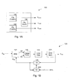
- Fig. 1A illustrates an exemplary embodiment of a tunable system employing concurrently operable frequency sources in accordance with the present invention.
- Fig. 1A illustrates an exemplary embodiment of a tunable system employing currently operable frequency sources in accordance with the present invention.
- the tunable system 100 includes three frequency sources FS 1 120, FS 2 130 and FS 3 140, at least two of which (e.g., FS 1 120) are tunable.
- the remaining frequency sources may be operable to generate a fixed frequency or a tunable frequency, as required or desired by the system's design.
- Fig. 1B illustrates an exemplary tunable frequency source in accordance with the present invention, the embodiment implemented as a sigma-delta phase locked loop (PLL).
- the PLL may be monolithically fabricated in a bipolar complementary metal oxide semiconductor (Bi-CMOS) process, although those of skill in the art will appreciate that the circuit may be formed using other processes or materials (e.g., CMOS, SiGe, GaAs) in monolithic, hybrid, or discrete form.
- Bi-CMOS bipolar complementary metal oxide semiconductor
- the frequency source 100 includes a phase-frequency detector 121, a charge pump circuit 122, loop filter 123, a tuning source 124 illustrated as bank of selectable VCOs, a main divide-by-N counter 125, and a programmable sigma-delta modulator 126.
- the sigma-delta modulator 126 receives a frequency setting control signal CNTL, and in response provides a scaling control data signal to the divide-by-N counter 125 to arrive at the desired divide ratio.
- the sigma-delta modulator 126 also receives the divide-by-N (F Div ) signal as a clock signal, thereby synchronizing its operation with the divide-by-N counter 125.
- tunable frequency source FS 1 120 is shown as a phase locked loop, other tunable frequency sources, such as variable oscillators, digitally controlled oscillators, and the like may be alternative employed.
- Fixed frequency sources may be implemented as L-C, dielectric resonator, crystal oscillators, and the like. The foregoing examples are only illustrative and those skilled in the art will appreciate that other frequency sources, both tunable and fixed, may be used in alternative embodiments of the present invention.
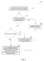
- Fig. 2 illustrates an exemplary method for relocating a prospective signal and an existing signal to provide sufficient frequency separation to avoid phase pulling effects. Only part of this method is in accordance with the present invention.
- the process begins at 212 where a prospective signal is requested having a frequency proximate to the frequency of an existing signal.
- a determination is made as to whether the prospective signal frequency is within the pulling bandwidth of the existing signal frequency.
- a database structure such as that shown in Fig.
- 3C of Applicant's copending application "Multiple Frequency Source System and Method of Operation” may be accessed to determine the frequency location of the most proximate existing signal and based thereon, a determination can be made if the prospective signal frequency would be within the pulling bandwidth of the existing signal frequency.
- the term "pulling bandwidth” refers to a threshold bandwidth within which the presense of a second signal “pulls” or modulates the subject signal, such that subject signal exceeds a predefined phase noise level.
- the pulling bandwidth of a subject signal will depend upon the desired phase noise level as well as several factors. For example, a frequency source exhibiting a relative high quality (Q) factor will have a relatively narrow pulling bandwidth for a given phase noise requirement. Similarly, a frequency source which is highly isolated from the frequency source generating the proximate signal will have a relatively narrow pulling bandwidth for the same phase noise requirement.
- the Q of a frequency source will depend upon its construction and architecture; e.g., a fixed frequency crystal or dielectric resonator oscillator may exhibit a higher Q than a tunable oscillator. Isolation of the frequency source (from other frequency sources) will also depend upon the construction and architecture of the multiple source system. In the limit, a frequency source exhibiting infinite Q, or infinite isolation from a frequency source generating a proximate signal will have a phase pulling bandwidth of 0 Hz, although these conditions would be impossible to obtain, especially in a particular embodiment of the invention in which multiple tunable sources are implemented on a single integrated circuit. Accordingly, a particular operating threshold is chosen to define the predefined pulling bandwidth.
- Exemplary embodiments of the pulling bandwidth of a signal include bandwidths less than 500 kHz, for example 250 kHz, 100 kHz, 50 kHz, or lower, as well as bandwidths greater than 500 kHz, for example 600 kHz, 700 kHz, 800 kHz, 900 kHz, 1 MHz, or wider bandwidths.
- the isolation and Q of the frequency sources are subsequently chosen (by calculation, by experiments, or by design simulations) in order to achieve the desired limit at the offset specified by the system (LO accuracy).
- the LO accuracy is specified to be ⁇ 1 MHz and the system is sized to give a spur at -45dBc at 500 kHz offset from the existing signal frequency, thus the pulling bandwidth is ⁇ 500 kHz, and the specified LO accuracy allow the LO to be placed more of 500 kHz away from the existing one in order to gain some margin on the spur level.
- the prospective signal frequency is determined to be within the predefined pulling bandwidth of the existing signal frequency
- the new prospective frequency point may, for example, represent a frequency point which is the least removed from the originally-requested prospective frequency point, but which is outside the pulling bandwidth.
- the operation 218 may involve two or more tuning operations, whereby the frequency source is tuned to a first frequency point, optionally checking to determine if the first frequency point is outside of the pulling bandwidth of the existing signal, and if not, identifying a second, further removed frequency point is identified, and the frequency source tuned thereto.
- the prospective signal is progressively stepped away from the existing signal until the required bandwidth separation from the existing signal is achieved (in accordance with the LO accuracy specified by the system).
- Those skilled in the art will appreciate that other techniques may be used to relocate the prospective signal out of the pulling bandwidth. Subsequently at 222, the prospective signal is generated at the new prospective frequency point.
- the process according to the current invention continues at 220, whereby the frequency point of the prospective signal is removed from within the pulling bandwidth. .
- the prospective signal frequency is tuned to a new prospective signal frequency point away from the existing signal frequency and outside of the pulling bandwidth
- the existing signal frequency is tuned from its present frequency point away from the prospective signal to a new existing frequency point
- a combination of (i) and (ii) whereby both the prospective and existing signal frequencies are tuned in opposite directions to respective new frequency points, each signal moved to a new frequency point such that the new prospective frequency point is located outside the pulling bandwidth of the new existing frequency point.
- process (i)-(iii) selected in 220 may be made dependent upon the tuning capability of the source.
- process (i) which does not form part of the invention, may be employed when the existing signal frequency source is located at a frequency extreme and cannot tune further away from the prospective signal, or if the existing signal is bein used or performing an operation which cannot be disturbed.
- Process (ii) which also does not form part of the invention, may be utilized when computations show that the prospective signal cannot be tuned any further from the existing signal.
- Process (iii) according to the invention can be used when both frequency sources have sufficient tuning latitude, and may be employed to minimize the frequency offset needed from each signal's original tuning point in order to obtain the required frequency spacing.
- the prospective and existing signals are tuned away from the other in a non-crossing manner, as exemplified in Fig. 3 below.
- the operations in 222 may be performed either in a single operation or in several operations.
- An examplary embodiment of the former may include, e.g., computing new frequency points which provides the required bandwidth separation to place the prospective signal frequency outside of the pulling bandwidth, and the prospective and existing frequencies generated at there respective frequency points.
- an iterative process may be performed, whereby one or both signals are gradually stepped away from each other, and optionally the resulting bandwidth separation checked to determine if the necessary bandwidth separation has been obtained to place the prospective signal outside of the pulling bandwidth.
- its frequency source may either be tuned from its original frequency point while continuing to generate the existing signal, or the existing signal may be deactivated, the frequency source configured to tune to the next existing frequency point, and the existing signal generated at that new frequency point.
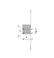
- Fig. 3 illustrates an exemplary method in which a prospective signal is relocated to provide sufficient bandwidth separation from an existing frequency signal to avoid frequency pulling.
- An existing signal 312 operates at a frequency point F E1 , the existing signal frequency having a predefined pulling bandwidth 320 associated therewith.
- a request is received to tune a prospective signal 322 to a first prospective frequency point F P1 , the first frequency point F P1 within the pulling bandwidth 320 of the existing frequency.
- the pulling bandwidth will generally be dependent upon the Q-factor of the frequency source, and the isolation between it and the frequency source generating the proximate signal.
- all of the frequency sources exhibit substantially the same Q-factor and isolation, and accordingly each frequency source will have substantially the same pulling bandwidth.
- the Q-factor and isolation is different for one or more of the frequency sources, and accordingly the pulling bandwidth will be determined once the tuning (second) frequency source is identified.
- F P1 lies within the pulling bandwidth 320
- the aforementioned process continues at 216 where a determination is made as to whether the existing signal 312 is generated by a tunable frequency source.
- the existing signal 312 is determined to be generated by a fixed frequency source.
- the tuning process continues at 218, where the prospective signal is relocated away from the first frequency point F P1 in a non-crossing manner to a second prospective frequency point F P2 .
- the tuning operation at 218 further includes determinating that F P2 is outside of the pulling bandwidth 320 of the existing signal 312.
- the process continues at 222 where the prospective signal 322 is generated at the second prospective frequency point F P2 .
- the process at 218 may be made iterative, whereby the prospective signal is gradually stepped away from the existing signal frequency in one or more steps.
- the relocation distance of each frequency would be less, as the combined effect of relocating the existing signal 312 slightly above F E1 (with the accompanying movement of the pulling bandwidth 320 also slightly higher in frequency) and moving the prospective signal 322 slightly below F T1 results in achieving the required bandwidth separation with comparably smaller frequency shifts.
- tunable systems such as the sigma-delta phase locked loop can be used as the frequency source for generating the existing and prospective signals.
- the existing frequency is iteratively tuned away from the prospective signal in two or more steps to reduce frequency overshoot effects which could accompany the signal's relocation to its final frequency.
- the frequency source may continue generating its signal during the signal's relocation to a new frequency point.
- the frequency source can be deactivated, configured to tune to the new frequency (e.g. a higher frequency), and activate its signal at the new frequency point.
- the described processes may be implemented in hardware, software, firmware or a combination of these implementations as appropriate.
- some or all of the described processes may be implemented as computer readable instruction code resident on a computer readable medium (removable disk, volatile or non-volatile memory, embedded processors, etc.), the instruction code operable to program a computer of other such programmable device to carry out the intended functions.
Landscapes
- Engineering & Computer Science (AREA)
- Theoretical Computer Science (AREA)
- Physics & Mathematics (AREA)
- Microelectronics & Electronic Packaging (AREA)
- General Engineering & Computer Science (AREA)
- General Physics & Mathematics (AREA)
- Computer Hardware Design (AREA)
- Stabilization Of Oscillater, Synchronisation, Frequency Synthesizers (AREA)
- Pulse Circuits (AREA)
- Superheterodyne Receivers (AREA)
- Measuring Volume Flow (AREA)
- Digital Transmission Methods That Use Modulated Carrier Waves (AREA)
- Networks Using Active Elements (AREA)
- Manipulation Of Pulses (AREA)
Applications Claiming Priority (4)
| Application Number | Priority Date | Filing Date | Title |
|---|---|---|---|
| US59575405P | 2005-08-02 | 2005-08-02 | |
| US59574905P | 2005-08-02 | 2005-08-02 | |
| US59575005P | 2005-08-02 | 2005-08-02 | |
| PCT/IB2006/052634 WO2007015211A2 (en) | 2005-08-02 | 2006-08-01 | System and method for mitigating phase pulling in a multiple frequency source system |
Publications (2)
| Publication Number | Publication Date |
|---|---|
| EP1911185A2 EP1911185A2 (en) | 2008-04-16 |
| EP1911185B1 true EP1911185B1 (en) | 2011-11-23 |
Family
ID=37467507
Family Applications (3)
| Application Number | Title | Priority Date | Filing Date |
|---|---|---|---|
| EP06766078A Withdrawn EP1910908A1 (en) | 2005-08-02 | 2006-08-01 | Offset signal phasing for a multiple frequency source system |
| EP06780271A Not-in-force EP1911185B1 (en) | 2005-08-02 | 2006-08-01 | System and method for mitigating phase pulling in a multiple frequency source system |
| EP06766077A Withdrawn EP1911159A1 (en) | 2005-08-02 | 2006-08-01 | Multiple frequency source system and method of operation |
Family Applications Before (1)
| Application Number | Title | Priority Date | Filing Date |
|---|---|---|---|
| EP06766078A Withdrawn EP1910908A1 (en) | 2005-08-02 | 2006-08-01 | Offset signal phasing for a multiple frequency source system |
Family Applications After (1)
| Application Number | Title | Priority Date | Filing Date |
|---|---|---|---|
| EP06766077A Withdrawn EP1911159A1 (en) | 2005-08-02 | 2006-08-01 | Multiple frequency source system and method of operation |
Country Status (6)
| Country | Link |
|---|---|
| US (3) | US7355483B2 (enExample) |
| EP (3) | EP1910908A1 (enExample) |
| JP (3) | JP2009504064A (enExample) |
| KR (4) | KR100853047B1 (enExample) |
| AT (1) | ATE535065T1 (enExample) |
| WO (3) | WO2007015211A2 (enExample) |
Cited By (1)
| Publication number | Priority date | Publication date | Assignee | Title |
|---|---|---|---|---|
| US9509353B2 (en) | 2014-08-20 | 2016-11-29 | Nxp B.V. | Data processing device |
Families Citing this family (18)
| Publication number | Priority date | Publication date | Assignee | Title |
|---|---|---|---|---|
| US7783467B2 (en) * | 2005-12-10 | 2010-08-24 | Electronics And Telecommunications Research Institute | Method for digital system modeling by using higher software simulator |
| US7474167B1 (en) * | 2006-08-31 | 2009-01-06 | Altera Corporation | Capacitance switch circuitry for digitally controlled oscillators |
| US7869781B2 (en) | 2006-12-06 | 2011-01-11 | Broadcom Corporation | Method and system for mitigating the effects of pulling in multiple phase locked loops in multi-standard systems |
| US20080143192A1 (en) * | 2006-12-14 | 2008-06-19 | Sample Alanson P | Dynamic radio frequency power harvesting |
| CN101197573B (zh) * | 2007-01-10 | 2010-12-29 | 晨星半导体股份有限公司 | 时脉产生器及应用其上的自我测试与切换控制方法 |
| JP2009010599A (ja) * | 2007-06-27 | 2009-01-15 | Panasonic Corp | デジタル制御発振回路、周波数シンセサイザ、それを用いた無線通信機器及びその制御方法 |
| US8212610B2 (en) * | 2008-09-19 | 2012-07-03 | Altera Corporation | Techniques for digital loop filters |
| KR101467417B1 (ko) * | 2008-12-30 | 2014-12-11 | 주식회사 동부하이텍 | 디지털 동기 회로 |
| US20100250746A1 (en) * | 2009-03-30 | 2010-09-30 | Hitachi, Ltd. | Information technology source migration |
| JP5148548B2 (ja) * | 2009-04-17 | 2013-02-20 | 株式会社東芝 | デジタルpll回路及び半導体集積回路 |
| WO2010134287A1 (ja) * | 2009-05-22 | 2010-11-25 | パナソニック株式会社 | Pll周波数シンセサイザ |
| US8756451B2 (en) * | 2011-10-01 | 2014-06-17 | Intel Corporation | Frequency synthesis methods and systems |
| US8692594B2 (en) * | 2011-12-19 | 2014-04-08 | Ati Technologies Ulc | Phase-locked loop frequency stepping |
| US9166604B2 (en) * | 2012-04-25 | 2015-10-20 | Infineon Technologies Ag | Timing monitor for PLL |
| US9490825B2 (en) * | 2013-05-23 | 2016-11-08 | Intel IP Corporation | Adjusting tuning segments in a digitally-controlled oscillator |
| GB201800174D0 (en) * | 2018-01-05 | 2018-02-21 | Kirintec Ltd | Receiver |
| CN111508416B (zh) * | 2020-04-30 | 2021-09-03 | 武汉华星光电半导体显示技术有限公司 | 显示器及其驱动方法 |
| CN115015870A (zh) * | 2022-05-27 | 2022-09-06 | 中国电子科技集团公司第十四研究所 | 一种多频率源间信号相位的同步方法 |
Family Cites Families (39)
| Publication number | Priority date | Publication date | Assignee | Title |
|---|---|---|---|---|
| JPS6120420A (ja) * | 1984-07-06 | 1986-01-29 | Nec Corp | 多相クロツク発生回路 |
| JP2541313B2 (ja) * | 1989-07-29 | 1996-10-09 | 日本電気株式会社 | デュアルpll装置 |
| US5452290A (en) * | 1992-10-26 | 1995-09-19 | Motorola, Inc. | Look ahead channel switching transceiver |
| US5408196A (en) | 1993-03-29 | 1995-04-18 | U.S. Philips Corporation | Tunable device |
| US6334219B1 (en) | 1994-09-26 | 2001-12-25 | Adc Telecommunications Inc. | Channel selection for a hybrid fiber coax network |
| US7339078B2 (en) * | 1995-03-10 | 2008-03-04 | G.D. Searle Llc | Bis-amino acid hydroxyethylamino sulfonamide retroviral protease inhibitors |
| US6177964B1 (en) * | 1997-08-01 | 2001-01-23 | Microtune, Inc. | Broadband integrated television tuner |
| JP3453006B2 (ja) * | 1995-07-07 | 2003-10-06 | パイオニア株式会社 | 位相同期回路及びディジタル信号再生装置 |
| US5774701A (en) * | 1995-07-10 | 1998-06-30 | Hitachi, Ltd. | Microprocessor operating at high and low clok frequencies |
| US5565816A (en) * | 1995-08-18 | 1996-10-15 | International Business Machines Corporation | Clock distribution network |
| JPH09246967A (ja) * | 1996-03-04 | 1997-09-19 | Casio Comput Co Ltd | Pll周波数シンセサイザ回路 |
| JP3323054B2 (ja) * | 1996-04-01 | 2002-09-09 | 株式会社東芝 | 周波数逓倍回路 |
| JP3596172B2 (ja) * | 1996-06-19 | 2004-12-02 | 富士通株式会社 | Pll周波数シンセサイザ |
| JPH10270999A (ja) * | 1997-03-24 | 1998-10-09 | Seiko Epson Corp | 半導体装置 |
| JP3279957B2 (ja) * | 1997-05-23 | 2002-04-30 | 松下電器産業株式会社 | 携帯無線装置 |
| JPH11205101A (ja) * | 1998-01-13 | 1999-07-30 | Toshiba Corp | 位相追従装置 |
| US6112308A (en) * | 1998-01-23 | 2000-08-29 | Intel Corporation | Cascaded multiple internal phase-locked loops for synchronization of hierarchically distinct chipset components and subsystems |
| SE513950C2 (sv) | 1998-02-12 | 2000-12-04 | Ericsson Telefon Ab L M | Förfarande och anordning i ett mobiltelekommunikationsnät för att åstadkomma en flerkanalsföbindelse |
| US6628779B1 (en) | 1998-05-11 | 2003-09-30 | Telcordia Technologies, Inc. | Method and system for scaleable near-end speech cancellation for tip and ring tone signal detectors |
| US6304146B1 (en) * | 1998-05-29 | 2001-10-16 | Silicon Laboratories, Inc. | Method and apparatus for synthesizing dual band high-frequency signals for wireless communications |
| JP2000286704A (ja) * | 1999-01-28 | 2000-10-13 | Matsushita Electric Ind Co Ltd | 周波数シンセサイザ装置とそれを用いた移動無線機 |
| JP2000341748A (ja) | 1999-04-15 | 2000-12-08 | Texas Instr Inc <Ti> | ワイヤレス通信システムにおける伝送資源割当て方法および周波数チャネルおよびタイムスロット割当てシステム |
| US6147561A (en) * | 1999-07-29 | 2000-11-14 | Conexant Systems, Inc. | Phase/frequency detector with time-delayed inputs in a charge pump based phase locked loop and a method for enhancing the phase locked loop gain |
| TW496035B (en) * | 2000-04-25 | 2002-07-21 | Univ Singapore | Method and apparatus for a digital clock multiplication circuit |
| JP2001332969A (ja) * | 2000-05-23 | 2001-11-30 | Nec Microsystems Ltd | 発振装置 |
| US6686803B1 (en) * | 2000-07-10 | 2004-02-03 | Silicon Laboratories, Inc. | Integrated circuit incorporating circuitry for determining which of at least two possible frequencies is present on an externally provided reference signal and method therefor |
| JP4454810B2 (ja) * | 2000-08-04 | 2010-04-21 | Necエレクトロニクス株式会社 | デジタル位相制御方法及びデジタル位相制御回路 |
| DE10102725C2 (de) | 2001-01-22 | 2003-04-24 | Infineon Technologies Ag | Verfahren zum Betreiben einer PLL-Frequenzsyntheseschaltung |
| JP2003133950A (ja) * | 2001-10-24 | 2003-05-09 | Nippon Dempa Kogyo Co Ltd | 入力切替電圧制御発振器及びpll制御発振器 |
| EP1318641A3 (en) * | 2001-12-10 | 2006-10-04 | Alps Electric Co., Ltd. | Carrier recovery with antenna diversity |
| US7062229B2 (en) * | 2002-03-06 | 2006-06-13 | Qualcomm Incorporated | Discrete amplitude calibration of oscillators in frequency synthesizers |
| US20030179842A1 (en) * | 2002-03-22 | 2003-09-25 | Kane Michael G. | Digital pattern sequence generator |
| JP2004072714A (ja) * | 2002-06-11 | 2004-03-04 | Rohm Co Ltd | クロック生成システム |
| KR100465455B1 (ko) | 2002-06-24 | 2005-01-13 | 씨제이 주식회사 | 2-티옥소티아졸 유도체, 그 제조방법 및 약제학적 조성물 |
| US20040006850A1 (en) | 2002-07-09 | 2004-01-15 | Wax David B. | Personal pen retaining system |
| JP4164301B2 (ja) * | 2002-07-16 | 2008-10-15 | 株式会社日立製作所 | 多周波pll発振器及びそれを用いた多周波cwレーダ |
| WO2004082277A1 (en) * | 2003-03-11 | 2004-09-23 | Thomson Licensing S.A. | Apparatus and method for distributing signals |
| US6954093B2 (en) | 2003-03-27 | 2005-10-11 | Micronas Gmbh | Clocking scheme and clock system for a monolithic integrated circuit |
| JP2006180398A (ja) * | 2004-12-24 | 2006-07-06 | Toshiba Corp | クロック生成装置およびクロック生成方法 |
-
2006
- 2006-08-01 AT AT06780271T patent/ATE535065T1/de active
- 2006-08-01 KR KR1020087002866A patent/KR100853047B1/ko not_active Expired - Fee Related
- 2006-08-01 JP JP2008524658A patent/JP2009504064A/ja active Pending
- 2006-08-01 JP JP2008524659A patent/JP4245658B2/ja not_active Expired - Fee Related
- 2006-08-01 EP EP06766078A patent/EP1910908A1/en not_active Withdrawn
- 2006-08-01 WO PCT/IB2006/052634 patent/WO2007015211A2/en not_active Ceased
- 2006-08-01 KR KR1020087005222A patent/KR100967723B1/ko not_active Expired - Fee Related
- 2006-08-01 US US11/461,534 patent/US7355483B2/en not_active Expired - Fee Related
- 2006-08-01 KR KR1020097009988A patent/KR100966926B1/ko not_active Expired - Fee Related
- 2006-08-01 WO PCT/IB2006/052633 patent/WO2007015210A1/en not_active Ceased
- 2006-08-01 US US11/461,530 patent/US7528665B2/en not_active Expired - Fee Related
- 2006-08-01 JP JP2008524657A patent/JP4395541B2/ja not_active Expired - Fee Related
- 2006-08-01 WO PCT/IB2006/052632 patent/WO2007015209A1/en not_active Ceased
- 2006-08-01 EP EP06780271A patent/EP1911185B1/en not_active Not-in-force
- 2006-08-01 KR KR1020087003990A patent/KR100917085B1/ko not_active Expired - Fee Related
- 2006-08-01 US US11/461,533 patent/US7653370B2/en not_active Expired - Fee Related
- 2006-08-01 EP EP06766077A patent/EP1911159A1/en not_active Withdrawn
Cited By (1)
| Publication number | Priority date | Publication date | Assignee | Title |
|---|---|---|---|---|
| US9509353B2 (en) | 2014-08-20 | 2016-11-29 | Nxp B.V. | Data processing device |
Also Published As
| Publication number | Publication date |
|---|---|
| US7528665B2 (en) | 2009-05-05 |
| KR100967723B1 (ko) | 2010-07-05 |
| KR100917085B1 (ko) | 2009-09-15 |
| JP4395541B2 (ja) | 2010-01-13 |
| US20070176663A1 (en) | 2007-08-02 |
| KR20080025766A (ko) | 2008-03-21 |
| US7355483B2 (en) | 2008-04-08 |
| US7653370B2 (en) | 2010-01-26 |
| KR20080023760A (ko) | 2008-03-14 |
| WO2007015211A2 (en) | 2007-02-08 |
| JP2009504064A (ja) | 2009-01-29 |
| EP1910908A1 (en) | 2008-04-16 |
| KR100853047B1 (ko) | 2008-08-19 |
| ATE535065T1 (de) | 2011-12-15 |
| KR20090058593A (ko) | 2009-06-09 |
| KR100966926B1 (ko) | 2010-06-29 |
| KR20080031503A (ko) | 2008-04-08 |
| JP4245658B2 (ja) | 2009-03-25 |
| JP2009504063A (ja) | 2009-01-29 |
| WO2007015210A1 (en) | 2007-02-08 |
| WO2007015209A1 (en) | 2007-02-08 |
| US20070200640A1 (en) | 2007-08-30 |
| WO2007015211A3 (en) | 2007-04-19 |
| US20070183014A1 (en) | 2007-08-09 |
| EP1911159A1 (en) | 2008-04-16 |
| EP1911185A2 (en) | 2008-04-16 |
| JP2009508369A (ja) | 2009-02-26 |
Similar Documents
| Publication | Publication Date | Title |
|---|---|---|
| EP1911185B1 (en) | System and method for mitigating phase pulling in a multiple frequency source system | |
| US8305115B2 (en) | Elimination of fractional N boundary spurs in a signal synthesizer | |
| US6414555B2 (en) | Frequency synthesizer | |
| US6057735A (en) | Amplifier for continuous high gain, narrowband signal amplification | |
| US9219487B1 (en) | Frequency ramp generation in PLL based RF frontend | |
| FR2711868A1 (fr) | Dispositif de commande automatique en fréquence. | |
| US4447792A (en) | Synthesizer circuit | |
| CN101719766B (zh) | 频率生成技术 | |
| CN101238658A (zh) | 用于在多频率源系统中减轻相位牵引的系统和方法 | |
| US8274337B2 (en) | Digital phase locked loop | |
| KR101692112B1 (ko) | 주파수 합성기의 주파수 보정 방법 및 장치 | |
| CN109995362B (zh) | 锁相环集成电路 | |
| JPH08256058A (ja) | 信号発生装置 | |
| KR102335966B1 (ko) | 위상잠금루프 회로를 이용한 다중 동기신호를 출력하는 다중 전압제어발진기 장치 | |
| JP2005151444A (ja) | 周波数シンセサイザ | |
| US6198354B1 (en) | System for limiting if variation in phase locked loops | |
| US20050036580A1 (en) | Programmable phase-locked loop fractional-N frequency synthesizer | |
| US7362767B2 (en) | Integrated circuit with on-chip clock frequency matching to upstream head end equipment | |
| CN118590013B (zh) | 基于现场可编程门阵列的可调制射频信号的产生方法 | |
| US6552617B1 (en) | Dual-tune input integrated VCO on a chip | |
| WO2025081910A1 (en) | Bandwidth boosting system | |
| CN108809302A (zh) | 一种锁相环频率综合器和频率控制方法 | |
| US20160373122A1 (en) | Frequency synthesizer circuit | |
| US20040027205A1 (en) | Local oscillator apparatus for low-noise generation of arbitrary frequencies | |
| JP2004350021A (ja) | Pll回路 |
Legal Events
| Date | Code | Title | Description |
|---|---|---|---|
| PUAI | Public reference made under article 153(3) epc to a published international application that has entered the european phase |
Free format text: ORIGINAL CODE: 0009012 |
|
| 17P | Request for examination filed |
Effective date: 20080123 |
|
| AK | Designated contracting states |
Kind code of ref document: A2 Designated state(s): AT BE BG CH CY CZ DE DK EE ES FI FR GB GR HU IE IS IT LI LT LU LV MC NL PL PT RO SE SI SK TR |
|
| 17Q | First examination report despatched |
Effective date: 20090902 |
|
| RAP1 | Party data changed (applicant data changed or rights of an application transferred) |
Owner name: RF MAGIC, INC. |
|
| GRAP | Despatch of communication of intention to grant a patent |
Free format text: ORIGINAL CODE: EPIDOSNIGR1 |
|
| DAX | Request for extension of the european patent (deleted) | ||
| GRAS | Grant fee paid |
Free format text: ORIGINAL CODE: EPIDOSNIGR3 |
|
| GRAA | (expected) grant |
Free format text: ORIGINAL CODE: 0009210 |
|
| AK | Designated contracting states |
Kind code of ref document: B1 Designated state(s): AT BE BG CH CY CZ DE DK EE ES FI FR GB GR HU IE IS IT LI LT LU LV MC NL PL PT RO SE SI SK TR |
|
| REG | Reference to a national code |
Ref country code: GB Ref legal event code: FG4D |
|
| REG | Reference to a national code |
Ref country code: CH Ref legal event code: EP |
|
| REG | Reference to a national code |
Ref country code: IE Ref legal event code: FG4D |
|
| REG | Reference to a national code |
Ref country code: DE Ref legal event code: R096 Ref document number: 602006026031 Country of ref document: DE Effective date: 20120119 |
|
| REG | Reference to a national code |
Ref country code: NL Ref legal event code: VDEP Effective date: 20111123 |
|
| LTIE | Lt: invalidation of european patent or patent extension |
Effective date: 20111123 |
|
| PG25 | Lapsed in a contracting state [announced via postgrant information from national office to epo] |
Ref country code: IS Free format text: LAPSE BECAUSE OF FAILURE TO SUBMIT A TRANSLATION OF THE DESCRIPTION OR TO PAY THE FEE WITHIN THE PRESCRIBED TIME-LIMIT Effective date: 20120323 Ref country code: LT Free format text: LAPSE BECAUSE OF FAILURE TO SUBMIT A TRANSLATION OF THE DESCRIPTION OR TO PAY THE FEE WITHIN THE PRESCRIBED TIME-LIMIT Effective date: 20111123 |
|
| PG25 | Lapsed in a contracting state [announced via postgrant information from national office to epo] |
Ref country code: LV Free format text: LAPSE BECAUSE OF FAILURE TO SUBMIT A TRANSLATION OF THE DESCRIPTION OR TO PAY THE FEE WITHIN THE PRESCRIBED TIME-LIMIT Effective date: 20111123 Ref country code: NL Free format text: LAPSE BECAUSE OF FAILURE TO SUBMIT A TRANSLATION OF THE DESCRIPTION OR TO PAY THE FEE WITHIN THE PRESCRIBED TIME-LIMIT Effective date: 20111123 Ref country code: SE Free format text: LAPSE BECAUSE OF FAILURE TO SUBMIT A TRANSLATION OF THE DESCRIPTION OR TO PAY THE FEE WITHIN THE PRESCRIBED TIME-LIMIT Effective date: 20111123 Ref country code: PT Free format text: LAPSE BECAUSE OF FAILURE TO SUBMIT A TRANSLATION OF THE DESCRIPTION OR TO PAY THE FEE WITHIN THE PRESCRIBED TIME-LIMIT Effective date: 20120323 Ref country code: BE Free format text: LAPSE BECAUSE OF FAILURE TO SUBMIT A TRANSLATION OF THE DESCRIPTION OR TO PAY THE FEE WITHIN THE PRESCRIBED TIME-LIMIT Effective date: 20111123 Ref country code: SI Free format text: LAPSE BECAUSE OF FAILURE TO SUBMIT A TRANSLATION OF THE DESCRIPTION OR TO PAY THE FEE WITHIN THE PRESCRIBED TIME-LIMIT Effective date: 20111123 Ref country code: GR Free format text: LAPSE BECAUSE OF FAILURE TO SUBMIT A TRANSLATION OF THE DESCRIPTION OR TO PAY THE FEE WITHIN THE PRESCRIBED TIME-LIMIT Effective date: 20120224 |
|
| PG25 | Lapsed in a contracting state [announced via postgrant information from national office to epo] |
Ref country code: CY Free format text: LAPSE BECAUSE OF FAILURE TO SUBMIT A TRANSLATION OF THE DESCRIPTION OR TO PAY THE FEE WITHIN THE PRESCRIBED TIME-LIMIT Effective date: 20111123 |
|
| PG25 | Lapsed in a contracting state [announced via postgrant information from national office to epo] |
Ref country code: CZ Free format text: LAPSE BECAUSE OF FAILURE TO SUBMIT A TRANSLATION OF THE DESCRIPTION OR TO PAY THE FEE WITHIN THE PRESCRIBED TIME-LIMIT Effective date: 20111123 Ref country code: BG Free format text: LAPSE BECAUSE OF FAILURE TO SUBMIT A TRANSLATION OF THE DESCRIPTION OR TO PAY THE FEE WITHIN THE PRESCRIBED TIME-LIMIT Effective date: 20120223 Ref country code: SK Free format text: LAPSE BECAUSE OF FAILURE TO SUBMIT A TRANSLATION OF THE DESCRIPTION OR TO PAY THE FEE WITHIN THE PRESCRIBED TIME-LIMIT Effective date: 20111123 Ref country code: DK Free format text: LAPSE BECAUSE OF FAILURE TO SUBMIT A TRANSLATION OF THE DESCRIPTION OR TO PAY THE FEE WITHIN THE PRESCRIBED TIME-LIMIT Effective date: 20111123 Ref country code: EE Free format text: LAPSE BECAUSE OF FAILURE TO SUBMIT A TRANSLATION OF THE DESCRIPTION OR TO PAY THE FEE WITHIN THE PRESCRIBED TIME-LIMIT Effective date: 20111123 |
|
| PG25 | Lapsed in a contracting state [announced via postgrant information from national office to epo] |
Ref country code: PL Free format text: LAPSE BECAUSE OF FAILURE TO SUBMIT A TRANSLATION OF THE DESCRIPTION OR TO PAY THE FEE WITHIN THE PRESCRIBED TIME-LIMIT Effective date: 20111123 Ref country code: IT Free format text: LAPSE BECAUSE OF FAILURE TO SUBMIT A TRANSLATION OF THE DESCRIPTION OR TO PAY THE FEE WITHIN THE PRESCRIBED TIME-LIMIT Effective date: 20111123 Ref country code: RO Free format text: LAPSE BECAUSE OF FAILURE TO SUBMIT A TRANSLATION OF THE DESCRIPTION OR TO PAY THE FEE WITHIN THE PRESCRIBED TIME-LIMIT Effective date: 20111123 |
|
| REG | Reference to a national code |
Ref country code: AT Ref legal event code: MK05 Ref document number: 535065 Country of ref document: AT Kind code of ref document: T Effective date: 20111123 |
|
| PGFP | Annual fee paid to national office [announced via postgrant information from national office to epo] |
Ref country code: LU Payment date: 20120831 Year of fee payment: 7 |
|
| PLBE | No opposition filed within time limit |
Free format text: ORIGINAL CODE: 0009261 |
|
| STAA | Information on the status of an ep patent application or granted ep patent |
Free format text: STATUS: NO OPPOSITION FILED WITHIN TIME LIMIT |
|
| 26N | No opposition filed |
Effective date: 20120824 |
|
| PGFP | Annual fee paid to national office [announced via postgrant information from national office to epo] |
Ref country code: GB Payment date: 20120828 Year of fee payment: 7 Ref country code: IE Payment date: 20120827 Year of fee payment: 7 |
|
| REG | Reference to a national code |
Ref country code: DE Ref legal event code: R097 Ref document number: 602006026031 Country of ref document: DE Effective date: 20120824 |
|
| PGFP | Annual fee paid to national office [announced via postgrant information from national office to epo] |
Ref country code: FR Payment date: 20120830 Year of fee payment: 7 Ref country code: DE Payment date: 20120829 Year of fee payment: 7 |
|
| PG25 | Lapsed in a contracting state [announced via postgrant information from national office to epo] |
Ref country code: AT Free format text: LAPSE BECAUSE OF FAILURE TO SUBMIT A TRANSLATION OF THE DESCRIPTION OR TO PAY THE FEE WITHIN THE PRESCRIBED TIME-LIMIT Effective date: 20111123 |
|
| PG25 | Lapsed in a contracting state [announced via postgrant information from national office to epo] |
Ref country code: ES Free format text: LAPSE BECAUSE OF FAILURE TO SUBMIT A TRANSLATION OF THE DESCRIPTION OR TO PAY THE FEE WITHIN THE PRESCRIBED TIME-LIMIT Effective date: 20120305 |
|
| PG25 | Lapsed in a contracting state [announced via postgrant information from national office to epo] |
Ref country code: FI Free format text: LAPSE BECAUSE OF FAILURE TO SUBMIT A TRANSLATION OF THE DESCRIPTION OR TO PAY THE FEE WITHIN THE PRESCRIBED TIME-LIMIT Effective date: 20111123 |
|
| REG | Reference to a national code |
Ref country code: CH Ref legal event code: PL |
|
| GBPC | Gb: european patent ceased through non-payment of renewal fee |
Effective date: 20130801 |
|
| PG25 | Lapsed in a contracting state [announced via postgrant information from national office to epo] |
Ref country code: LI Free format text: LAPSE BECAUSE OF NON-PAYMENT OF DUE FEES Effective date: 20130831 Ref country code: TR Free format text: LAPSE BECAUSE OF FAILURE TO SUBMIT A TRANSLATION OF THE DESCRIPTION OR TO PAY THE FEE WITHIN THE PRESCRIBED TIME-LIMIT Effective date: 20111123 Ref country code: DE Free format text: LAPSE BECAUSE OF NON-PAYMENT OF DUE FEES Effective date: 20140301 Ref country code: CH Free format text: LAPSE BECAUSE OF NON-PAYMENT OF DUE FEES Effective date: 20130831 |
|
| REG | Reference to a national code |
Ref country code: IE Ref legal event code: MM4A |
|
| REG | Reference to a national code |
Ref country code: DE Ref legal event code: R119 Ref document number: 602006026031 Country of ref document: DE Effective date: 20140301 |
|
| REG | Reference to a national code |
Ref country code: FR Ref legal event code: ST Effective date: 20140430 |
|
| PG25 | Lapsed in a contracting state [announced via postgrant information from national office to epo] |
Ref country code: GB Free format text: LAPSE BECAUSE OF NON-PAYMENT OF DUE FEES Effective date: 20130801 Ref country code: IE Free format text: LAPSE BECAUSE OF NON-PAYMENT OF DUE FEES Effective date: 20130801 Ref country code: HU Free format text: LAPSE BECAUSE OF FAILURE TO SUBMIT A TRANSLATION OF THE DESCRIPTION OR TO PAY THE FEE WITHIN THE PRESCRIBED TIME-LIMIT Effective date: 20060801 |
|
| PG25 | Lapsed in a contracting state [announced via postgrant information from national office to epo] |
Ref country code: FR Free format text: LAPSE BECAUSE OF NON-PAYMENT OF DUE FEES Effective date: 20130902 |
|
| PGFP | Annual fee paid to national office [announced via postgrant information from national office to epo] |
Ref country code: MC Payment date: 20140722 Year of fee payment: 9 |
|
| PG25 | Lapsed in a contracting state [announced via postgrant information from national office to epo] |
Ref country code: LU Free format text: LAPSE BECAUSE OF NON-PAYMENT OF DUE FEES Effective date: 20130801 |
|
| PG25 | Lapsed in a contracting state [announced via postgrant information from national office to epo] |
Ref country code: MC Free format text: LAPSE BECAUSE OF NON-PAYMENT OF DUE FEES Effective date: 20150831 |