EP1891452B1 - Current sensor - Google Patents
Current sensor Download PDFInfo
- Publication number
- EP1891452B1 EP1891452B1 EP06770974A EP06770974A EP1891452B1 EP 1891452 B1 EP1891452 B1 EP 1891452B1 EP 06770974 A EP06770974 A EP 06770974A EP 06770974 A EP06770974 A EP 06770974A EP 1891452 B1 EP1891452 B1 EP 1891452B1
- Authority
- EP
- European Patent Office
- Prior art keywords
- current
- conductor portion
- substrate
- hall effect
- current sensor
- Prior art date
- Legal status (The legal status is an assumption and is not a legal conclusion. Google has not performed a legal analysis and makes no representation as to the accuracy of the status listed.)
- Active
Links
Images


Classifications
-
- G—PHYSICS
- G01—MEASURING; TESTING
- G01R—MEASURING ELECTRIC VARIABLES; MEASURING MAGNETIC VARIABLES
- G01R15/00—Details of measuring arrangements of the types provided for in groups G01R17/00 - G01R29/00, G01R33/00 - G01R33/26 or G01R35/00
- G01R15/14—Adaptations providing voltage or current isolation, e.g. for high-voltage or high-current networks
- G01R15/20—Adaptations providing voltage or current isolation, e.g. for high-voltage or high-current networks using galvano-magnetic devices, e.g. Hall-effect devices, i.e. measuring a magnetic field via the interaction between a current and a magnetic field, e.g. magneto resistive or Hall effect devices
- G01R15/207—Constructional details independent of the type of device used
-
- G—PHYSICS
- G01—MEASURING; TESTING
- G01R—MEASURING ELECTRIC VARIABLES; MEASURING MAGNETIC VARIABLES
- G01R15/00—Details of measuring arrangements of the types provided for in groups G01R17/00 - G01R29/00, G01R33/00 - G01R33/26 or G01R35/00
- G01R15/14—Adaptations providing voltage or current isolation, e.g. for high-voltage or high-current networks
- G01R15/20—Adaptations providing voltage or current isolation, e.g. for high-voltage or high-current networks using galvano-magnetic devices, e.g. Hall-effect devices, i.e. measuring a magnetic field via the interaction between a current and a magnetic field, e.g. magneto resistive or Hall effect devices
- G01R15/202—Adaptations providing voltage or current isolation, e.g. for high-voltage or high-current networks using galvano-magnetic devices, e.g. Hall-effect devices, i.e. measuring a magnetic field via the interaction between a current and a magnetic field, e.g. magneto resistive or Hall effect devices using Hall-effect devices
-
- H—ELECTRICITY
- H01—ELECTRIC ELEMENTS
- H01L—SEMICONDUCTOR DEVICES NOT COVERED BY CLASS H10
- H01L23/00—Details of semiconductor or other solid state devices
- H01L23/552—Protection against radiation, e.g. light or electromagnetic waves
-
- H—ELECTRICITY
- H01—ELECTRIC ELEMENTS
- H01L—SEMICONDUCTOR DEVICES NOT COVERED BY CLASS H10
- H01L24/00—Arrangements for connecting or disconnecting semiconductor or solid-state bodies; Methods or apparatus related thereto
- H01L24/01—Means for bonding being attached to, or being formed on, the surface to be connected, e.g. chip-to-package, die-attach, "first-level" interconnects; Manufacturing methods related thereto
- H01L24/34—Strap connectors, e.g. copper straps for grounding power devices; Manufacturing methods related thereto
- H01L24/36—Structure, shape, material or disposition of the strap connectors prior to the connecting process
- H01L24/37—Structure, shape, material or disposition of the strap connectors prior to the connecting process of an individual strap connector
-
- H—ELECTRICITY
- H01—ELECTRIC ELEMENTS
- H01L—SEMICONDUCTOR DEVICES NOT COVERED BY CLASS H10
- H01L24/00—Arrangements for connecting or disconnecting semiconductor or solid-state bodies; Methods or apparatus related thereto
- H01L24/01—Means for bonding being attached to, or being formed on, the surface to be connected, e.g. chip-to-package, die-attach, "first-level" interconnects; Manufacturing methods related thereto
- H01L24/34—Strap connectors, e.g. copper straps for grounding power devices; Manufacturing methods related thereto
- H01L24/39—Structure, shape, material or disposition of the strap connectors after the connecting process
- H01L24/40—Structure, shape, material or disposition of the strap connectors after the connecting process of an individual strap connector
-
- H—ELECTRICITY
- H01—ELECTRIC ELEMENTS
- H01L—SEMICONDUCTOR DEVICES NOT COVERED BY CLASS H10
- H01L24/00—Arrangements for connecting or disconnecting semiconductor or solid-state bodies; Methods or apparatus related thereto
- H01L24/01—Means for bonding being attached to, or being formed on, the surface to be connected, e.g. chip-to-package, die-attach, "first-level" interconnects; Manufacturing methods related thereto
- H01L24/34—Strap connectors, e.g. copper straps for grounding power devices; Manufacturing methods related thereto
- H01L24/39—Structure, shape, material or disposition of the strap connectors after the connecting process
- H01L24/41—Structure, shape, material or disposition of the strap connectors after the connecting process of a plurality of strap connectors
-
- H—ELECTRICITY
- H01—ELECTRIC ELEMENTS
- H01L—SEMICONDUCTOR DEVICES NOT COVERED BY CLASS H10
- H01L24/00—Arrangements for connecting or disconnecting semiconductor or solid-state bodies; Methods or apparatus related thereto
- H01L24/73—Means for bonding being of different types provided for in two or more of groups H01L24/10, H01L24/18, H01L24/26, H01L24/34, H01L24/42, H01L24/50, H01L24/63, H01L24/71
-
- H—ELECTRICITY
- H01—ELECTRIC ELEMENTS
- H01L—SEMICONDUCTOR DEVICES NOT COVERED BY CLASS H10
- H01L24/00—Arrangements for connecting or disconnecting semiconductor or solid-state bodies; Methods or apparatus related thereto
- H01L24/91—Methods for connecting semiconductor or solid state bodies including different methods provided for in two or more of groups H01L24/80 - H01L24/90
-
- H—ELECTRICITY
- H10—SEMICONDUCTOR DEVICES; ELECTRIC SOLID-STATE DEVICES NOT OTHERWISE PROVIDED FOR
- H10N—ELECTRIC SOLID-STATE DEVICES NOT OTHERWISE PROVIDED FOR
- H10N52/00—Hall-effect devices
-
- G—PHYSICS
- G01—MEASURING; TESTING
- G01R—MEASURING ELECTRIC VARIABLES; MEASURING MAGNETIC VARIABLES
- G01R1/00—Details of instruments or arrangements of the types included in groups G01R5/00 - G01R13/00 and G01R31/00
- G01R1/02—General constructional details
- G01R1/18—Screening arrangements against electric or magnetic fields, e.g. against earth's field
-
- H—ELECTRICITY
- H01—ELECTRIC ELEMENTS
- H01L—SEMICONDUCTOR DEVICES NOT COVERED BY CLASS H10
- H01L2224/00—Indexing scheme for arrangements for connecting or disconnecting semiconductor or solid-state bodies and methods related thereto as covered by H01L24/00
- H01L2224/01—Means for bonding being attached to, or being formed on, the surface to be connected, e.g. chip-to-package, die-attach, "first-level" interconnects; Manufacturing methods related thereto
- H01L2224/34—Strap connectors, e.g. copper straps for grounding power devices; Manufacturing methods related thereto
- H01L2224/36—Structure, shape, material or disposition of the strap connectors prior to the connecting process
- H01L2224/37—Structure, shape, material or disposition of the strap connectors prior to the connecting process of an individual strap connector
- H01L2224/37001—Core members of the connector
- H01L2224/37099—Material
- H01L2224/371—Material with a principal constituent of the material being a metal or a metalloid, e.g. boron [B], silicon [Si], germanium [Ge], arsenic [As], antimony [Sb], tellurium [Te] and polonium [Po], and alloys thereof
- H01L2224/37138—Material with a principal constituent of the material being a metal or a metalloid, e.g. boron [B], silicon [Si], germanium [Ge], arsenic [As], antimony [Sb], tellurium [Te] and polonium [Po], and alloys thereof the principal constituent melting at a temperature of greater than or equal to 950°C and less than 1550°C
- H01L2224/37147—Copper [Cu] as principal constituent
-
- H—ELECTRICITY
- H01—ELECTRIC ELEMENTS
- H01L—SEMICONDUCTOR DEVICES NOT COVERED BY CLASS H10
- H01L2224/00—Indexing scheme for arrangements for connecting or disconnecting semiconductor or solid-state bodies and methods related thereto as covered by H01L24/00
- H01L2224/01—Means for bonding being attached to, or being formed on, the surface to be connected, e.g. chip-to-package, die-attach, "first-level" interconnects; Manufacturing methods related thereto
- H01L2224/34—Strap connectors, e.g. copper straps for grounding power devices; Manufacturing methods related thereto
- H01L2224/36—Structure, shape, material or disposition of the strap connectors prior to the connecting process
- H01L2224/37—Structure, shape, material or disposition of the strap connectors prior to the connecting process of an individual strap connector
- H01L2224/3754—Coating
- H01L2224/37599—Material
- H01L2224/37686—Material with a principal constituent of the material being a non metallic, non metalloid inorganic material
-
- H—ELECTRICITY
- H01—ELECTRIC ELEMENTS
- H01L—SEMICONDUCTOR DEVICES NOT COVERED BY CLASS H10
- H01L2224/00—Indexing scheme for arrangements for connecting or disconnecting semiconductor or solid-state bodies and methods related thereto as covered by H01L24/00
- H01L2224/01—Means for bonding being attached to, or being formed on, the surface to be connected, e.g. chip-to-package, die-attach, "first-level" interconnects; Manufacturing methods related thereto
- H01L2224/34—Strap connectors, e.g. copper straps for grounding power devices; Manufacturing methods related thereto
- H01L2224/36—Structure, shape, material or disposition of the strap connectors prior to the connecting process
- H01L2224/37—Structure, shape, material or disposition of the strap connectors prior to the connecting process of an individual strap connector
- H01L2224/3754—Coating
- H01L2224/37599—Material
- H01L2224/3769—Material with a principal constituent of the material being a polymer, e.g. polyester, phenolic based polymer, epoxy
-
- H—ELECTRICITY
- H01—ELECTRIC ELEMENTS
- H01L—SEMICONDUCTOR DEVICES NOT COVERED BY CLASS H10
- H01L2224/00—Indexing scheme for arrangements for connecting or disconnecting semiconductor or solid-state bodies and methods related thereto as covered by H01L24/00
- H01L2224/01—Means for bonding being attached to, or being formed on, the surface to be connected, e.g. chip-to-package, die-attach, "first-level" interconnects; Manufacturing methods related thereto
- H01L2224/34—Strap connectors, e.g. copper straps for grounding power devices; Manufacturing methods related thereto
- H01L2224/39—Structure, shape, material or disposition of the strap connectors after the connecting process
- H01L2224/40—Structure, shape, material or disposition of the strap connectors after the connecting process of an individual strap connector
- H01L2224/4005—Shape
- H01L2224/4009—Loop shape
- H01L2224/40095—Kinked
-
- H—ELECTRICITY
- H01—ELECTRIC ELEMENTS
- H01L—SEMICONDUCTOR DEVICES NOT COVERED BY CLASS H10
- H01L2224/00—Indexing scheme for arrangements for connecting or disconnecting semiconductor or solid-state bodies and methods related thereto as covered by H01L24/00
- H01L2224/01—Means for bonding being attached to, or being formed on, the surface to be connected, e.g. chip-to-package, die-attach, "first-level" interconnects; Manufacturing methods related thereto
- H01L2224/34—Strap connectors, e.g. copper straps for grounding power devices; Manufacturing methods related thereto
- H01L2224/39—Structure, shape, material or disposition of the strap connectors after the connecting process
- H01L2224/40—Structure, shape, material or disposition of the strap connectors after the connecting process of an individual strap connector
- H01L2224/401—Disposition
- H01L2224/40151—Connecting between a semiconductor or solid-state body and an item not being a semiconductor or solid-state body, e.g. chip-to-substrate, chip-to-passive
- H01L2224/40221—Connecting between a semiconductor or solid-state body and an item not being a semiconductor or solid-state body, e.g. chip-to-substrate, chip-to-passive the body and the item being stacked
- H01L2224/40245—Connecting between a semiconductor or solid-state body and an item not being a semiconductor or solid-state body, e.g. chip-to-substrate, chip-to-passive the body and the item being stacked the item being metallic
-
- H—ELECTRICITY
- H01—ELECTRIC ELEMENTS
- H01L—SEMICONDUCTOR DEVICES NOT COVERED BY CLASS H10
- H01L2224/00—Indexing scheme for arrangements for connecting or disconnecting semiconductor or solid-state bodies and methods related thereto as covered by H01L24/00
- H01L2224/01—Means for bonding being attached to, or being formed on, the surface to be connected, e.g. chip-to-package, die-attach, "first-level" interconnects; Manufacturing methods related thereto
- H01L2224/42—Wire connectors; Manufacturing methods related thereto
- H01L2224/47—Structure, shape, material or disposition of the wire connectors after the connecting process
- H01L2224/48—Structure, shape, material or disposition of the wire connectors after the connecting process of an individual wire connector
- H01L2224/481—Disposition
- H01L2224/48151—Connecting between a semiconductor or solid-state body and an item not being a semiconductor or solid-state body, e.g. chip-to-substrate, chip-to-passive
- H01L2224/48221—Connecting between a semiconductor or solid-state body and an item not being a semiconductor or solid-state body, e.g. chip-to-substrate, chip-to-passive the body and the item being stacked
- H01L2224/48245—Connecting between a semiconductor or solid-state body and an item not being a semiconductor or solid-state body, e.g. chip-to-substrate, chip-to-passive the body and the item being stacked the item being metallic
- H01L2224/48247—Connecting between a semiconductor or solid-state body and an item not being a semiconductor or solid-state body, e.g. chip-to-substrate, chip-to-passive the body and the item being stacked the item being metallic connecting the wire to a bond pad of the item
-
- H—ELECTRICITY
- H01—ELECTRIC ELEMENTS
- H01L—SEMICONDUCTOR DEVICES NOT COVERED BY CLASS H10
- H01L2224/00—Indexing scheme for arrangements for connecting or disconnecting semiconductor or solid-state bodies and methods related thereto as covered by H01L24/00
- H01L2224/01—Means for bonding being attached to, or being formed on, the surface to be connected, e.g. chip-to-package, die-attach, "first-level" interconnects; Manufacturing methods related thereto
- H01L2224/42—Wire connectors; Manufacturing methods related thereto
- H01L2224/47—Structure, shape, material or disposition of the wire connectors after the connecting process
- H01L2224/48—Structure, shape, material or disposition of the wire connectors after the connecting process of an individual wire connector
- H01L2224/481—Disposition
- H01L2224/48151—Connecting between a semiconductor or solid-state body and an item not being a semiconductor or solid-state body, e.g. chip-to-substrate, chip-to-passive
- H01L2224/48221—Connecting between a semiconductor or solid-state body and an item not being a semiconductor or solid-state body, e.g. chip-to-substrate, chip-to-passive the body and the item being stacked
- H01L2224/48245—Connecting between a semiconductor or solid-state body and an item not being a semiconductor or solid-state body, e.g. chip-to-substrate, chip-to-passive the body and the item being stacked the item being metallic
- H01L2224/4826—Connecting between the body and an opposite side of the item with respect to the body
-
- H—ELECTRICITY
- H01—ELECTRIC ELEMENTS
- H01L—SEMICONDUCTOR DEVICES NOT COVERED BY CLASS H10
- H01L2224/00—Indexing scheme for arrangements for connecting or disconnecting semiconductor or solid-state bodies and methods related thereto as covered by H01L24/00
- H01L2224/73—Means for bonding being of different types provided for in two or more of groups H01L2224/10, H01L2224/18, H01L2224/26, H01L2224/34, H01L2224/42, H01L2224/50, H01L2224/63, H01L2224/71
- H01L2224/732—Location after the connecting process
- H01L2224/73201—Location after the connecting process on the same surface
- H01L2224/73215—Layer and wire connectors
-
- H—ELECTRICITY
- H01—ELECTRIC ELEMENTS
- H01L—SEMICONDUCTOR DEVICES NOT COVERED BY CLASS H10
- H01L2224/00—Indexing scheme for arrangements for connecting or disconnecting semiconductor or solid-state bodies and methods related thereto as covered by H01L24/00
- H01L2224/73—Means for bonding being of different types provided for in two or more of groups H01L2224/10, H01L2224/18, H01L2224/26, H01L2224/34, H01L2224/42, H01L2224/50, H01L2224/63, H01L2224/71
- H01L2224/732—Location after the connecting process
- H01L2224/73201—Location after the connecting process on the same surface
- H01L2224/73221—Strap and wire connectors
-
- H—ELECTRICITY
- H01—ELECTRIC ELEMENTS
- H01L—SEMICONDUCTOR DEVICES NOT COVERED BY CLASS H10
- H01L24/00—Arrangements for connecting or disconnecting semiconductor or solid-state bodies; Methods or apparatus related thereto
- H01L24/01—Means for bonding being attached to, or being formed on, the surface to be connected, e.g. chip-to-package, die-attach, "first-level" interconnects; Manufacturing methods related thereto
- H01L24/42—Wire connectors; Manufacturing methods related thereto
- H01L24/47—Structure, shape, material or disposition of the wire connectors after the connecting process
- H01L24/48—Structure, shape, material or disposition of the wire connectors after the connecting process of an individual wire connector
-
- H—ELECTRICITY
- H01—ELECTRIC ELEMENTS
- H01L—SEMICONDUCTOR DEVICES NOT COVERED BY CLASS H10
- H01L2924/00—Indexing scheme for arrangements or methods for connecting or disconnecting semiconductor or solid-state bodies as covered by H01L24/00
- H01L2924/0001—Technical content checked by a classifier
- H01L2924/00014—Technical content checked by a classifier the subject-matter covered by the group, the symbol of which is combined with the symbol of this group, being disclosed without further technical details
-
- H—ELECTRICITY
- H01—ELECTRIC ELEMENTS
- H01L—SEMICONDUCTOR DEVICES NOT COVERED BY CLASS H10
- H01L2924/00—Indexing scheme for arrangements or methods for connecting or disconnecting semiconductor or solid-state bodies as covered by H01L24/00
- H01L2924/01—Chemical elements
- H01L2924/01005—Boron [B]
-
- H—ELECTRICITY
- H01—ELECTRIC ELEMENTS
- H01L—SEMICONDUCTOR DEVICES NOT COVERED BY CLASS H10
- H01L2924/00—Indexing scheme for arrangements or methods for connecting or disconnecting semiconductor or solid-state bodies as covered by H01L24/00
- H01L2924/01—Chemical elements
- H01L2924/01006—Carbon [C]
-
- H—ELECTRICITY
- H01—ELECTRIC ELEMENTS
- H01L—SEMICONDUCTOR DEVICES NOT COVERED BY CLASS H10
- H01L2924/00—Indexing scheme for arrangements or methods for connecting or disconnecting semiconductor or solid-state bodies as covered by H01L24/00
- H01L2924/01—Chemical elements
- H01L2924/01013—Aluminum [Al]
-
- H—ELECTRICITY
- H01—ELECTRIC ELEMENTS
- H01L—SEMICONDUCTOR DEVICES NOT COVERED BY CLASS H10
- H01L2924/00—Indexing scheme for arrangements or methods for connecting or disconnecting semiconductor or solid-state bodies as covered by H01L24/00
- H01L2924/01—Chemical elements
- H01L2924/01015—Phosphorus [P]
-
- H—ELECTRICITY
- H01—ELECTRIC ELEMENTS
- H01L—SEMICONDUCTOR DEVICES NOT COVERED BY CLASS H10
- H01L2924/00—Indexing scheme for arrangements or methods for connecting or disconnecting semiconductor or solid-state bodies as covered by H01L24/00
- H01L2924/01—Chemical elements
- H01L2924/01024—Chromium [Cr]
-
- H—ELECTRICITY
- H01—ELECTRIC ELEMENTS
- H01L—SEMICONDUCTOR DEVICES NOT COVERED BY CLASS H10
- H01L2924/00—Indexing scheme for arrangements or methods for connecting or disconnecting semiconductor or solid-state bodies as covered by H01L24/00
- H01L2924/01—Chemical elements
- H01L2924/01029—Copper [Cu]
-
- H—ELECTRICITY
- H01—ELECTRIC ELEMENTS
- H01L—SEMICONDUCTOR DEVICES NOT COVERED BY CLASS H10
- H01L2924/00—Indexing scheme for arrangements or methods for connecting or disconnecting semiconductor or solid-state bodies as covered by H01L24/00
- H01L2924/01—Chemical elements
- H01L2924/01033—Arsenic [As]
-
- H—ELECTRICITY
- H01—ELECTRIC ELEMENTS
- H01L—SEMICONDUCTOR DEVICES NOT COVERED BY CLASS H10
- H01L2924/00—Indexing scheme for arrangements or methods for connecting or disconnecting semiconductor or solid-state bodies as covered by H01L24/00
- H01L2924/01—Chemical elements
- H01L2924/01047—Silver [Ag]
-
- H—ELECTRICITY
- H01—ELECTRIC ELEMENTS
- H01L—SEMICONDUCTOR DEVICES NOT COVERED BY CLASS H10
- H01L2924/00—Indexing scheme for arrangements or methods for connecting or disconnecting semiconductor or solid-state bodies as covered by H01L24/00
- H01L2924/01—Chemical elements
- H01L2924/01074—Tungsten [W]
-
- H—ELECTRICITY
- H01—ELECTRIC ELEMENTS
- H01L—SEMICONDUCTOR DEVICES NOT COVERED BY CLASS H10
- H01L2924/00—Indexing scheme for arrangements or methods for connecting or disconnecting semiconductor or solid-state bodies as covered by H01L24/00
- H01L2924/01—Chemical elements
- H01L2924/01079—Gold [Au]
-
- H—ELECTRICITY
- H01—ELECTRIC ELEMENTS
- H01L—SEMICONDUCTOR DEVICES NOT COVERED BY CLASS H10
- H01L2924/00—Indexing scheme for arrangements or methods for connecting or disconnecting semiconductor or solid-state bodies as covered by H01L24/00
- H01L2924/01—Chemical elements
- H01L2924/01082—Lead [Pb]
-
- H—ELECTRICITY
- H01—ELECTRIC ELEMENTS
- H01L—SEMICONDUCTOR DEVICES NOT COVERED BY CLASS H10
- H01L2924/00—Indexing scheme for arrangements or methods for connecting or disconnecting semiconductor or solid-state bodies as covered by H01L24/00
- H01L2924/013—Alloys
- H01L2924/0132—Binary Alloys
- H01L2924/01322—Eutectic Alloys, i.e. obtained by a liquid transforming into two solid phases
-
- H—ELECTRICITY
- H01—ELECTRIC ELEMENTS
- H01L—SEMICONDUCTOR DEVICES NOT COVERED BY CLASS H10
- H01L2924/00—Indexing scheme for arrangements or methods for connecting or disconnecting semiconductor or solid-state bodies as covered by H01L24/00
- H01L2924/013—Alloys
- H01L2924/014—Solder alloys
-
- H—ELECTRICITY
- H01—ELECTRIC ELEMENTS
- H01L—SEMICONDUCTOR DEVICES NOT COVERED BY CLASS H10
- H01L2924/00—Indexing scheme for arrangements or methods for connecting or disconnecting semiconductor or solid-state bodies as covered by H01L24/00
- H01L2924/10—Details of semiconductor or other solid state devices to be connected
- H01L2924/11—Device type
- H01L2924/13—Discrete devices, e.g. 3 terminal devices
- H01L2924/1304—Transistor
- H01L2924/1306—Field-effect transistor [FET]
-
- H—ELECTRICITY
- H01—ELECTRIC ELEMENTS
- H01L—SEMICONDUCTOR DEVICES NOT COVERED BY CLASS H10
- H01L2924/00—Indexing scheme for arrangements or methods for connecting or disconnecting semiconductor or solid-state bodies as covered by H01L24/00
- H01L2924/10—Details of semiconductor or other solid state devices to be connected
- H01L2924/11—Device type
- H01L2924/14—Integrated circuits
-
- H—ELECTRICITY
- H01—ELECTRIC ELEMENTS
- H01L—SEMICONDUCTOR DEVICES NOT COVERED BY CLASS H10
- H01L2924/00—Indexing scheme for arrangements or methods for connecting or disconnecting semiconductor or solid-state bodies as covered by H01L24/00
- H01L2924/15—Details of package parts other than the semiconductor or other solid state devices to be connected
- H01L2924/181—Encapsulation
-
- H—ELECTRICITY
- H01—ELECTRIC ELEMENTS
- H01L—SEMICONDUCTOR DEVICES NOT COVERED BY CLASS H10
- H01L2924/00—Indexing scheme for arrangements or methods for connecting or disconnecting semiconductor or solid-state bodies as covered by H01L24/00
- H01L2924/30—Technical effects
- H01L2924/301—Electrical effects
- H01L2924/3025—Electromagnetic shielding
Definitions
- This invention relates generally to electrical current sensors, and more particularly to a miniaturized current sensor in an integrated circuit package.
- one type of conventional current sensor uses a magnetic field transducer (for example a Hall effect or magnetoresistive transducer) in proximity to a current conductor.
- the magnetic field transducer generates an output signal having a magnitude proportional to the magnetic field induced by a current that flows through the current conductor.
- Some typical Hall effect current sensors include a gapped toroid magnetic flux concentrator, with the Hall effect element positioned in the toroid gap.
- the Hall effect device and toroid are assembled into a housing, which is mountable on a printed circuit board.
- a separate current conductor, such as a wire is passed through the center of the toroid.
- Such devices tend to be undesirably large, both in terms of height and circuit board area.
- Hall effect current sensors include a Hall effect element mounted on a dielectric material, for example a circuit board.
- a Hall effect element mounted on a dielectric material for example a circuit board.
- One such current sensor is described in a European Patent Application No. EP0867725 .
- Still other Hall effect current sensors include a Hall effect element mounted on a substrate, for example a silicon substrate as described in a European Patent Application No. EP1111693 .
- Sensitivity is related to the magnitude of a change in output voltage from the Hall effect transducer in response to a sensed current.
- Linearity is related to the degree to which the output voltage from the Hall effect transducer varies in direct proportion to the sensed current.
- the sensitivity of a current sensor is related to a variety of factors.
- One important factor is the flux concentration of the magnetic field generated in the vicinity of the current conductor and sensed by the Hall effect element. For this reason, some current sensors use a flux concentrator.
- US 2005/045359 A1 discloses an integrated circuit current sensor including a lead frame having at least two leads coupled to provide a current conductor portion, and a substrate having a first surface in which is disposed one or more magnetic field transducers, with the first surface being proximate the current conductor portion and a second surface distal from the current conductor portion.
- the substrate is disposed having the first surface of the substrate above the current conductor portion and the second surface of the substrate above the first surface.
- the substrate is oriented upside-down in the integrated circuit relative to a conventional orientation. With this arrangement, a current sensor is provided for which the one or more magnetic field transducers are very close to the current conductor portion, resulting in a current sensor having improved sensitivity.
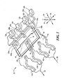
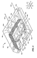
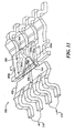
- an exemplary current sensor 10 includes a lead frame 12 having a plurality of leads 12a-12h.
- the leads 12a and 12b are coupled to the leads 12c and 12d to form a current path, or current conductor with a narrow portion 14 having a width w1.
- the current sensor 10 also includes a substrate 16 having a first surface 16a and a second, opposing surface 16b.
- the substrate 16 has a magnetic field transducer 18 which, in some arrangements, can be a Hall effect element 18, diffused into the first surface 16a, or otherwise disposed on the first surface 16a.
- the substrate 16 can be comprised of a semiconductor material, e.g., silicon, or, in an alternate arrangement, the substrate 16 can be comprised of an insulating material.
- the substrate 16 is disposed above the lead frame 12 so that the first surface 16a is proximate to the current conductor portion 14 and the second surface 16b is distal from the current conductor portion 14 and more specifically, so that the Hall effect element 18 is in close proximity to the current conductor portion 14.
- the substrate 16 has an orientation that is upside down (i.e., the first surface 16a is directed downward) relative to a conventional orientation with which a substrate is mounted in an integrated circuit package.
- the substrate 16 has bonding pads 20a-20c on the first surface 16a, to which bond wires 22a-22c are coupled.
- the bond wires are further coupled to the leads 12e, 12f, 12h of the lead frame 12.
- the Hall effect element 18 is disposed in close proximity to the current conductor portion 14 and at a predetermined position relative to the conductor portion 14, such that a magnetic field generated by an electrical current passing though the current conductor portion 14, in a direction shown by arrows 26, is in a direction substantially aligned with a maximum response axis of the Hall effect element 18.
- the Hall effect element 18 generates a voltage output proportional to the magnetic field and therefore proportional to the current flowing through the current conductor portion 14.
- the illustrated Hall effect element 18 has a maximum response axis substantially aligned with a z-axis 34.
- the Hall affect element 18 is disposed just to the side (i.e., slightly offset along a y-axis 32) of the current conductor portion 14, as shown, where the magnetic field is pointed substantially along the z-axis 34. This position results in a greater voltage output from the Hall effect element 18, and therefore improved sensitivity.
- a Hall effect element, or another type of magnetic field sensor, for example a magnetoresistance element, having maximum response axis aligned in another direction can be disposed at another position relative to the current conductor portion 14, for example, on top of the current conductor portion 14 (in a direction along z-axis 34)
- a graph 50 illustrates the magnetic flux density in the direction of the z-axis 34 ( FIG. 1 ) across the Hall element 18, along an x-axis 30 ( FIG. 1 ) and the y-axis 32 ( FIG. 1 ) in the plane of the Hall effect element 18 ( FIG. 1 ), for a current-through current conductor portion 14 on the order or 10A.
- a center (not shown) of the Hall effect element 18 corresponds to three hundred microns on an abscissa 52.
- a mantissa 54 corresponds to magnetic flux.
- the width w1 ( FIG. 1 ) of the current conductor portion 14 in the x-direction 30 relative to the dimension of the Hall effect element 18 in the x-direction 30 significantly affects the uniformity of the flux density in the z-direction 34 with position along the Hall effect element 18 in the x-direction 30.
- the longer the current conductor portion 14 i.e., the greater the width w1, FIG. 1 ), relative to the width of the Hall effect element 18 in the x-direction 30, the longer the curve 56 remains substantially flat.
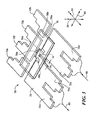
- another exemplary currant sensor 70 includes a lead frame 72 having a plurality of leads 72a-72h and a current conductor portion 74 having a width w2.
- the current sensor also includes a substrate 76 having a first surface 76a and a second, opposing surface 76b.
- the substrate 76 has first and second Hall effect elements 78a, 78b diffused into the first surface 76a, or otherwise disposed on or supported by the first surface 76a.
- the substrate 76 is disposed on the lead frame 72 so that the Hall effect element 78 is in close proximity to the current conductor portion 74.
- the substrate 76 has an orientation that is upside down (i.e., the first surface 76a is directed downward) in relation to the conventional orientation of a substrate mounted in an integrated circuit package.
- An insulator (not shown) can separate the substrate 76 from the lead frame 72.
- the insulator can be the same as or similar to the insulator 24 shown in FIG. 1 .
- the current sensor 70 is relatively insensitive to variation in the position of the Hall effect elements 78a, 78b in the direction of the y-axis 92. This is because, when moved in the direction of the y-axis 92, the voltage output from one of the Hall effect elements 78a, 78b tends to increase while the voltage output from the other of the Hall effect elements 78a, 78b tends to decrease. Therefore, the differential sum of the two outputs remains relatively invariant.
- lead frame 72 is shown to have the flat leads 72a-72h suitable for surface amounting to a circuit board, it will be appreciated that a lead frame having bent leads, like the lead frame 12 of FIG. 1 , can also be used. Also, while two Hall effect elements 78a, 78b are shown, more than two or fewer than two Hall effect elements can also be used.
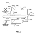
- a summing circuit 100 suitable for performing the differential signal summation described in conjunction with FIG. 3 is shown coupled to two Hall effect elements 102a, 102b.
- the Hall effect elements 102a, 102b can be the same as or similar to the Hall effect elements 78a, 78b of FIG. 3 .
- each of the Hall effect elements 102a, 102b is rotated relative to the other Hall effect element by 90 degrees, as indicated by vectors on the Hall effect elements 102a, 102b. Therefore, in response to opposite magnetic fields 112a, 112b the Hall effect elements 102a, 102b generate output voltages 103a, 103b having the same polarities.
- the output voltage 103 a is coupled to amplifier 104a arranged in a non-inverting configuration and the output voltage 103b is coupled to the amplifier 104b arranged in an inverting configuration. Therefore, the amplifier output voltages 106a, 106b move in opposite voltage directions in response to the magnetic fields 112a, 112b.
- the amplifier output voltages 106a, 106b are differentially coupled to an amplifier 108 to generate a differential summation, or a difference of the output voltages 106a, 106b. Therefore, the output voltages 106a, 106b differentially sum to provide a greater output voltages 110 at the output of amplifier 108.
- the summing circuit 100 can be used in the current sensor 70 of FIG. 3 , in which case Hall effect elements 102a, 102b correspond to the Hall affect elements 78a, 78b.
- the summing circuit 100 is diffused into, or otherwise disposed upon, the first surface 76a of the substrate 76.
- the summing circuit 100 is diffused into, or otherwise disposed upon, the second surface 76b of the substrate 76, while the Hall effect elements 78a, 78b remain on the first surface 76a, coupled to the other circuit components though vias or the like.
- another exemplary current sensor 120 includes a substrate 126 having a first surface 126a and a second, opposing surface 126b.
- four Hall effect elements 128a-128d are diffused into or otherwise disposed on the first surface 126a of the substrate 126.
- the substrate 126 is positioned relative to the lead frame 12 such that first and second Hall effect element 128a, 128b respectively are on one side of the current conductor portion 14 along a y-axis 142, and third and fourth Hall effect elements 128c, 128d are on the opposite side of the current conductor portion 14 along the y-axis 42, as shown.
- the Hall effect elements 128a, 128b are offset (along the y-axis 142) from the current conductor portion 14 by an amount equal to and opposite from the amount that the Hall effect elements 128c, 128d are offset (along the y-axis 142) from the current conductor portion 14.
- first and second Hall effect elements 128a, 128b are exposed to a magnetic field in a direction along the z-axis 144 and the third and forth Hall effect elements 128c, 128d are exposed to a magnetic fields in the opposite direction along the z-axis 144.
- the four Hall effect elements 128a-128d coupled to a summing circuit as described, in the presence of the current, provide a voltage output four times the magnitude of a voltage output from a single Hall effect element, for example, the Hall effect element 18 of FIG. 1 , in the presence of the same current.
- the current sensor 120 has four times the sensitivity of the current sensor 10 of FIG. 1 .
- the current sensor 120 is relatively insensitive to variation in the position of the Hall effect elements 128a-128d in the direction of the y-axis 142. This is because, when moved in the direction of the y-axis 142, the voltage output from two of the four Hall effect elements 128a-128d tends to increase while the voltage output from the other two of the four Hall effect elements 128a-128d tends to decrease. Therefore, when coupled as a summing circuit, the circuit output is relatively invariant to the y-axis position of the Hall effect elements.
- the Hall effect element 158 is disposed in close proximity to the current conductor portion 154 and at a predetermined position relative to the conductor portion 154, such that a magnetic field generated by an electrical current passing though the current conductor portion 154 in a direction shown by arrows 168, is in a direction substantially aligned with a maximum response axis of the Hall effect element 158.
- the Hall effect element 158 has a maximum response axis aligned with a z-axis 174. Therefore, the Hall effect element 158 is disposed just to the side (i.e., slight offset along a y-axis 172) of the current conductor portion 14, as shown, where the magnetic field is pointed along the z-axis 174.
- Hall effect element 158 is shown on the first surface 166a of the substrate 166, it will be appreciated that more than one Hall effect element can be used.
- Other circuitry for example an amplifier, can also be diffused in or otherwise coupled to or supported by the first and/or second surfaces 166a, 166b of the substrate 166.
- an exemplary current sensor 180 includes a flux concentrator 182 and a flux concentrating layer 184.
- the flux concentrator is located proximate the Hall effect sensor 158, adjacent to and below the first surface 166a of the substrate 166
- the flux concentrating layer 184 is disposed on (or adjacent to and above) the second surface 166b of the substrate 166.
- the flux concentrator 182 is shown having a cubic shape, in other arrangements, the flux concentrator can have another shape, for example, a polyhedral shape, an elliptical shape, or a spherical shape. While both the flux concentrator 182 and the flux concentrating layer 184 are shown, in other arrangements, only one of the flux concentrator 182 and the flux concentrating layer 184 can be provided. Also, while the flux concentrator 182 and the flux concentrating layer 184 are shown in conjunction with one magnetic field transducer 158, it should be appreciated that the flux concentrator 182 and the flux concentrating layer 184 can also be applied to configurations having more than the one magnetic field transducer 158, for example, the configurations shown in FIGS. 1 , 3 , and 5 .
- the Hall effect elements 78a, 78b experience a greater magnetic field, resulting in a more sensitive current sensor.
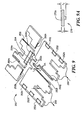
- an alternate current conductor portion 270 suitable fox replacing the current conductor portion 254 of FIG, 9 , has a T-shaped cross section as would be seen from a cross-section taken along line 9A-9A of FIG. 9 .
- the T-shape has a surface 270a, a first thickness t3, and a second thickness t4.
- the thickness t3 can be the same as or similar to the thickness t1 of FIG. 9
- the thickness t4 can be the same as or similar to the thickness t2 of FIG. 9 .
- the thickness t3 is approximately half of the thickness t4.
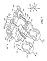
- another exemplary current sensor 300 includes a lead frame 302 (also referred to herein as a lead frame portion) having a plurality of leads 302a-302h and a current conductor portion 304 provided as a combination of a first current conductor portion 304a and a second current conductor portion 304b.
- the current sensor 300 also includes a substrate 306 having a first surface 306a and a second, opposing, surface 306b.
- the substrate 306 has a Hall effect element 308 diffused into the first surface 306a, or otherwise disposed on or supported by the first surface 306a.
- the substrate 306 is disposed on the lead frame 302 so that the Hall effect element 308 is in close proximity to the current conductor portion 304.
- the spin depositing process can result in a substrate insulting layer comprised of a variety materials, including but not limited to a polymer, for example, polyimide (e.g., trade name Pyralin®) or bisbenzocyclobutene (BCB) (e.g., trade name Cyclotene®).
- the sputtering process can result in a substrate insulting layer comprised of a variety materials, including but not limited to, nitride or oxide.
- the PECVD process can result in a substrate insulting layer comprised of a variety materials, including but not limited to, nitride or oxide.
- the LPCVD process can result in a substrate insulting layer comprised of a variety materials, including but not limited to, nitride or oxide.
- the insulating layer 330 is a substrate insulating layer associated with the substrate 306
- the insulating layer 330 is a substrate oxide insulating layer formed with an oxide generation process.
- the substrate oxide insulating layer can be comprised, for example, of a silicon dioxide.
- the current 316 flows into the leads 302c, 302d, which are coupled in parallel, through the current conductor portion 304, and out of the leads 302a, 302b, which are also coupled in parallel.
- the current flowing though the current conductor portion 304 generates a magnetic field, which is sensed by the Hall effect element 308.
- the Hall effect element 308 is in very close proximity to the current conductor portion 304 and at a predetermined position relative to the current conductor portion 304 at which the magnetic field generated by the current is substantially aligned with the maximum response axis of the Hall effect element 308. This placement results in a greater voltage output from the Hall effect element 308, and therefore greater sensitivity.
- lead frame 302 is shown to have the bent leads 302a-302h suitable for surface mounting to a circuit board, it will be appreciated that a lead frame having leads with other shapes can also be used, including but not limited to, through hole leads having a straight shape.
- An insulating layer 402 is disposed between the current conductor portion 304a and the first surface 306a of the substrate 306.
- the insulating layer 402 is an interposing insulating layer, for example a ceramic layer as described above in conjunction with Fig. 10 .
- insulating layer 402 is a substrate insulating layer associated with the substrate.
- the insulating layer 402 is a lead frame insulating layer associated with the lead frame 302. It will be appreciated that, when associated with the lead frame, the insulating layer 402 can extend beyond the substrate 306 in a direction along the y-axis 324. This arrangement provides enhanced reliability, since an edge of the substrate 306 is less likely to contact the lead frame 302.
- Interposing insulating layers and substrate insulating layers are described above, in conjunction with FIG. 10 .
- the insulating layer 402 is a lead frame insulating layer associated with the lead frame 302
- the insulating layer 402 is a lead frame sprayed insulating layer formed with a spraying process.
- the lead frame sprayed insulting layer can be comprised of a variety of materials, including but not limited to a polymer, for example, a polyimide (e.g., trade name Pyralin®), a bisbenzocyclobutene (BCB) (e.g., trade name Cyclotene®) a sprayed dielectric, (e.g., trade names 3M Scotch® Insulating Spray 1601 and Loctite® ShadowCure® 3900), or a spray ceramic coating.
- a polyimide e.g., trade name Pyralin®
- BCB bisbenzocyclobutene
- Cyclotene® a sprayed dielectric
- trade names 3M Scotch® Insulating Spray 1601 and Loctite® ShadowCure® 3900
- the insulating layer 402 is a lead frame insulating layer associated with the lead frame 302
- the insulating layer 402 is a lead frame oxide insulating layer formed with an oxide generation process.
- the lead frame oxide insulating layer can be comprised, for example, of a sputtered oxide layer disposed onto the lead frame 3 02.
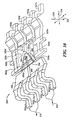
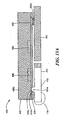
- another exemplary current sensor 450 includes a lead frame 452 (also referred to herein as a lead frame portion) having a plurality of leads 452a-452h and a current conductor portion 454.
- the lead frame 452 can be similar to the lead frame 302 of FIG. 12 .
- the current sensor 450 also includes a substrate 456 having a first surface 456a and a second, opposing, surface 456b.
- the substrate 456 has a Hall effect element 458 diffused into the first surface 456a, or otherwise disposed on or supported by the first surface 456a.
- the substrate 456 is disposed on the lead frame 452 so that the Hall effect element 458 is in close proximity to the current conductor portion 454.
- the substrate 456 has an orientation that is upside down (i.e., the first surface 456a is directed downward) in relation to the conventional orientation of a substrate mounted in an integrated circuit package.
- the substrate 456 is arranged as a flip-chip having solder balls 460a-460e on the first surface 456a of the substrate 456.
- the solder balls 460a-460e couple directly to the leads 452e-452h.
- An insulating layer 470 can separate the substrate 456 from the lead frame 452.
- the insulating layer 470 can be the same as or similar to the insulator 24 shown in FIG. 1 .
- the insulating layer 470 can cover a substantial portion of the surface 456a.
- the insulating layer has regions 470a, 470b, which are devoid of insulating material, as will become more apparent from the discussion of FIG. 13A below.
- the insulating layer 470 is an interposing insulating layer, for example a ceramic layer. In other arrangements, the insulating layer 470 is a substrate insulating layer associated with the substrate. In other arrangements, the insulating layer 470 is a lead frame insulating layer associated with the lead frame 452.
- another exemplary current sensor 500 includes a lead frame 502 having a plurality of leads 502a-502h. Only leads 502c and 502d shown for clarity, however, it will be understood that other ones of the leads 502a-502h are arranged in a conventional lead arrangement.
- the current sensor 500 also includes a substrate 506 having a first surface 506a and a second, opposing, surface 506b.
- the substrate 506 has a Hall effect element 508 diffused into the first surface 506a, or otherwise disposed on the first surface 506as
- a conductive clip 503 having a current conductor portion 504 is coupled to the leads 502a-502d.
- the current conductor portion 504 includes two bumps 504a, 504b.
- the bumps 504a, 504b align with and extent into the regions 514a, 514b of the insulating layer 514, which are devoid of insulating material.
- the bumps 504a, 504b have a size and a shape selected to provide electrical contact between the current conductor portion 504 and the first surface 506a of the substrate 506.
- the two bumps 504a, 504b provide electrical contact to metalized features (not shown) upon the first surface 506a. of the substrate 506, providing electrical coupling to circuits (not shown) also disposed on the first surface 506a of the substrate 506. The electrical coupling and the circuits coupled thereto are discussed below in greater detail in conjunction with FIG. 15 .
- the second current conductor portion can be the same as or similar to the second current conductor portion 304b of FIG. 10 , and can be similarly disposed upon the first surface 506a of the substrate 506 or upon the insulator 514.
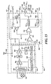
- the Hall effect element 552 is coupled to a current sensing circuit 554, which includes a dynamic offset cancellation circuit 553.
- the dynamic offset cancellation circuit 553 provides a DC offset adjustment for DC voltage errors associated with the Hall effect element 552.
- the dynamic offset cancellation circuit 553 is coupled to an amplifier 556 that amplifies the offset adjusted Hall output signal.
- the amplifier 556 is coupled to a filter 558 that can be a low pass filter, a high pass falter, a band pass filter, and/or a notch filter.
- the filter 558 is selected in accordance with a variety of factors including, but not limited to, a desired response time, and a frequency spectrum of noise associated with the Hall effect element 552, the dynamic offset cancellation circuit 553, and the amplifier 556.
- the filter 558 is a low pass filter.
- the filter 558 is coupled to an output driver 560 that provides a current sensor output signal 571 at a node 572 for transmission to other electronics (not shown). As described more fully below, the current sensor output signal is indicative of a magnitude of a current passing though a conductor.
- a trim control circuit 564 is coupled to node 570.
- the node 570 can receive a trim signal that permits various current sensor parameters to be trimmed, typically during manufacture.
- the trim control circuit 564 includes one or more counters enabled by an appropriate signal applied to the node 570.
- the trim control circuit 564 is coupled to a quiescent output voltage (Qvo) circuit 562.
- the quiescent output voltage is the voltage of the output signal 571 when the current sensed by the Hall effect element 552 is zero. Nominally, for a unipolar supply voltage, Qvo is equal to Vcc/2. Qvo can be trimmed by applying a suitable trim signal through the node 570 to a first trim control circuit counter within the trim control circuit 564, which, in turn, controls a digital-to-analog converter (DAC) within the Qvo circuit 562.
- DAC digital-to-analog converter
- an overcurrent circuit 590 can detect the overcurrent condition.
- the current conductor portion 304 provides a current path for a portion of the current 316
- the shunt conductor portion 706 provides another current path for another portion of the current 316.
- the current sensor 700 has a sensitivity to the current 316 related to the portion of the current 316 that flows through the current conductor portion 304.
- the current sensor 700 can have a lower sensitivity to the current 316 than the current sensor 300 of FIG. 10 , which does not have the shunt conductor portion 706. Therefore, the current sensor 700 can operate over a greater range of currents without saturating circuitry coupled to the Hall effect element 308 (e.g., the circuit 554 of FIG. 15 ).
- Sizing of the shunt conductor portion 706 in a way that affects a resistance of the shunt conductor portion 706 can influence the portion of the current 316 flowing through the shunt conductor portion 706 relative to the portion of the current 316 flowing through the current conductor portion 304.
- a size and a shape of the shunt conductor portion 706 can be selected accordingly to provide a selected resistance. Therefore, the sizing can effect the overall sensitivity of the current sensor 700
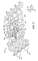
- the slit 806 tends to reduce a size (i.e., a diameter or path length) of the closed loops in which the eddy currents 812, 814 travel. It will be understood that the reduced size of the closed loops in which the eddy currents 812, 814 travel results in smaller eddy currants 812, 814 and a smaller local effect on the AC magnetic field that induced the eddy current. Therefore, the sensitivity of a current sensor on which the Hall effect element 816 and the electromagnetic shield 800 are used is less affected by the smaller eddy currents.
- the electromagnetic shield 900 is able to support eddy currents having a much smaller size (i.e., diameter of path length) than the electromagnetic shield 850 of FIG. 20 or the electromagnetic shield 800 of FIG. 19 . Therefore, the electromagnetic shield 900 tends to have an even smaller negative affect on sensitivity of a current sensor than that described above.
Landscapes
- Physics & Mathematics (AREA)
- Engineering & Computer Science (AREA)
- Computer Hardware Design (AREA)
- Microelectronics & Electronic Packaging (AREA)
- Power Engineering (AREA)
- General Physics & Mathematics (AREA)
- Health & Medical Sciences (AREA)
- Electromagnetism (AREA)
- Toxicology (AREA)
- Condensed Matter Physics & Semiconductors (AREA)
- Measuring Instrument Details And Bridges, And Automatic Balancing Devices (AREA)
- Hall/Mr Elements (AREA)
- Lead Frames For Integrated Circuits (AREA)
- Investigating Or Analyzing Materials By The Use Of Electric Means (AREA)
- Measuring Fluid Pressure (AREA)
Priority Applications (4)
| Application Number | Priority Date | Filing Date | Title |
|---|---|---|---|
| EP09000121A EP2163908B1 (en) | 2005-05-27 | 2006-05-23 | Current sensor |
| EP09000122.3A EP2402770B1 (en) | 2005-05-27 | 2006-05-23 | Current sensor |
| EP09000123.1A EP2157436B1 (en) | 2005-05-27 | 2006-05-23 | Current sensor |
| EP10183958.7A EP2295993B1 (en) | 2005-05-27 | 2006-05-23 | Current Sensor |
Applications Claiming Priority (6)
| Application Number | Priority Date | Filing Date | Title |
|---|---|---|---|
| US11/140,250 US6995315B2 (en) | 2003-08-26 | 2005-05-27 | Current sensor |
| US11/144,970 US7166807B2 (en) | 2003-08-26 | 2005-06-03 | Current sensor |
| US11/336,602 US7075287B1 (en) | 2003-08-26 | 2006-01-20 | Current sensor |
| US11/401,160 US7476816B2 (en) | 2003-08-26 | 2006-04-10 | Current sensor |
| US11/383,021 US20060219436A1 (en) | 2003-08-26 | 2006-05-12 | Current sensor |
| PCT/US2006/019953 WO2006130393A1 (en) | 2005-05-27 | 2006-05-23 | Current sensor |
Related Child Applications (4)
| Application Number | Title | Priority Date | Filing Date |
|---|---|---|---|
| EP09000123.1A Division EP2157436B1 (en) | 2005-05-27 | 2006-05-23 | Current sensor |
| EP09000121A Division EP2163908B1 (en) | 2005-05-27 | 2006-05-23 | Current sensor |
| EP09000122.3A Division EP2402770B1 (en) | 2005-05-27 | 2006-05-23 | Current sensor |
| EP10183958.7A Division EP2295993B1 (en) | 2005-05-27 | 2006-05-23 | Current Sensor |
Publications (2)
| Publication Number | Publication Date |
|---|---|
| EP1891452A1 EP1891452A1 (en) | 2008-02-27 |
| EP1891452B1 true EP1891452B1 (en) | 2009-09-16 |
Family
ID=36955377
Family Applications (5)
| Application Number | Title | Priority Date | Filing Date |
|---|---|---|---|
| EP09000123.1A Active EP2157436B1 (en) | 2005-05-27 | 2006-05-23 | Current sensor |
| EP10183958.7A Active EP2295993B1 (en) | 2005-05-27 | 2006-05-23 | Current Sensor |
| EP09000121A Active EP2163908B1 (en) | 2005-05-27 | 2006-05-23 | Current sensor |
| EP09000122.3A Active EP2402770B1 (en) | 2005-05-27 | 2006-05-23 | Current sensor |
| EP06770974A Active EP1891452B1 (en) | 2005-05-27 | 2006-05-23 | Current sensor |
Family Applications Before (4)
| Application Number | Title | Priority Date | Filing Date |
|---|---|---|---|
| EP09000123.1A Active EP2157436B1 (en) | 2005-05-27 | 2006-05-23 | Current sensor |
| EP10183958.7A Active EP2295993B1 (en) | 2005-05-27 | 2006-05-23 | Current Sensor |
| EP09000121A Active EP2163908B1 (en) | 2005-05-27 | 2006-05-23 | Current sensor |
| EP09000122.3A Active EP2402770B1 (en) | 2005-05-27 | 2006-05-23 | Current sensor |
Country Status (7)
| Country | Link |
|---|---|
| US (2) | US20060219436A1 (OSRAM) |
| EP (5) | EP2157436B1 (OSRAM) |
| JP (1) | JP5468776B2 (OSRAM) |
| KR (1) | KR101231830B1 (OSRAM) |
| AT (1) | ATE443266T1 (OSRAM) |
| DE (1) | DE602006009256D1 (OSRAM) |
| WO (1) | WO2006130393A1 (OSRAM) |
Cited By (2)
| Publication number | Priority date | Publication date | Assignee | Title |
|---|---|---|---|---|
| US9228860B2 (en) | 2006-07-14 | 2016-01-05 | Allegro Microsystems, Llc | Sensor and method of providing a sensor |
| DE112010004674B4 (de) * | 2009-12-03 | 2016-06-02 | Allegro Microsystems, Llc | Verfahren und Vorrichtung für ein erhöhtes Frequenzansprechverhalten von magnetischen Fühlern |
Families Citing this family (182)
| Publication number | Priority date | Publication date | Assignee | Title |
|---|---|---|---|---|
| US6853178B2 (en) * | 2000-06-19 | 2005-02-08 | Texas Instruments Incorporated | Integrated circuit leadframes patterned for measuring the accurate amplitude of changing currents |
| US20060219436A1 (en) * | 2003-08-26 | 2006-10-05 | Taylor William P | Current sensor |
| US7768083B2 (en) | 2006-01-20 | 2010-08-03 | Allegro Microsystems, Inc. | Arrangements for an integrated sensor |
| US7687882B2 (en) * | 2006-04-14 | 2010-03-30 | Allegro Microsystems, Inc. | Methods and apparatus for integrated circuit having multiple dies with at least one on chip capacitor |
| US7573112B2 (en) * | 2006-04-14 | 2009-08-11 | Allegro Microsystems, Inc. | Methods and apparatus for sensor having capacitor on chip |
| US20070279053A1 (en) * | 2006-05-12 | 2007-12-06 | Taylor William P | Integrated current sensor |
| US9823090B2 (en) | 2014-10-31 | 2017-11-21 | Allegro Microsystems, Llc | Magnetic field sensor for sensing a movement of a target object |
| US7936164B2 (en) * | 2008-07-03 | 2011-05-03 | Allegro Microsystems, Inc. | Folding current sensor |
| US8093670B2 (en) | 2008-07-24 | 2012-01-10 | Allegro Microsystems, Inc. | Methods and apparatus for integrated circuit having on chip capacitor with eddy current reductions |
| US8063634B2 (en) * | 2008-07-31 | 2011-11-22 | Allegro Microsystems, Inc. | Electronic circuit and method for resetting a magnetoresistance element |
| US20100052424A1 (en) * | 2008-08-26 | 2010-03-04 | Taylor William P | Methods and apparatus for integrated circuit having integrated energy storage device |
| US9222992B2 (en) * | 2008-12-18 | 2015-12-29 | Infineon Technologies Ag | Magnetic field current sensors |
| US20110006763A1 (en) * | 2009-07-07 | 2011-01-13 | Anthonius Bakker | Hall effect current sensor system and associated flip-chip packaging |
| JP5620989B2 (ja) * | 2009-07-22 | 2014-11-05 | アレグロ・マイクロシステムズ・エルエルシー | 磁界センサの診断動作モードを生成するための回路および方法 |
| CH702193A2 (de) * | 2009-11-05 | 2011-05-13 | Polycontact Ag | Positionsmeldeeinrichtung. |
| JP5500956B2 (ja) * | 2009-11-26 | 2014-05-21 | 本田技研工業株式会社 | 電流検出装置 |
| DE102009047235A1 (de) * | 2009-11-27 | 2011-06-01 | Robert Bosch Gmbh | Schaltungseinrichtung und Leistungsschaltkreis mit der Schaltungseinrichtung |
| US8717016B2 (en) * | 2010-02-24 | 2014-05-06 | Infineon Technologies Ag | Current sensors and methods |
| US10111333B2 (en) * | 2010-03-16 | 2018-10-23 | Intersil Americas Inc. | Molded power-supply module with bridge inductor over other components |
| US9013890B2 (en) | 2010-03-26 | 2015-04-21 | Infineon Technologies Ag | Semiconductor packages and methods for producing the same |
| US8760149B2 (en) | 2010-04-08 | 2014-06-24 | Infineon Technologies Ag | Magnetic field current sensors |
| US8461824B2 (en) * | 2010-06-07 | 2013-06-11 | Infineon Technologies Ag | Current sensor |
| US8680843B2 (en) * | 2010-06-10 | 2014-03-25 | Infineon Technologies Ag | Magnetic field current sensors |
| US8283742B2 (en) | 2010-08-31 | 2012-10-09 | Infineon Technologies, A.G. | Thin-wafer current sensors |
| US9723766B2 (en) | 2010-09-10 | 2017-08-01 | Intersil Americas LLC | Power supply module with electromagnetic-interference (EMI) shielding, cooling, or both shielding and cooling, along two or more sides |
| RU2453853C2 (ru) * | 2010-09-27 | 2012-06-20 | Федеральное Государственное Унитарное Предприятие "Государственный научно-производственный ракетно-космический центр "ЦСКБ-Прогресс" (ФГУП "ГНПРКЦ "ЦСКБ-Прогресс") | Способ измерения силы тока в проводнике и устройство для его осуществления |
| CH703903B1 (de) | 2010-10-01 | 2014-04-30 | Melexis Tessenderlo Nv | Stromsensor. |
| JP5556603B2 (ja) * | 2010-11-10 | 2014-07-23 | 三菱電機株式会社 | 磁気アイソレータ |
| US8878531B2 (en) | 2010-11-18 | 2014-11-04 | Infineon Technologies Ag | Current sensor |
| US9103853B2 (en) | 2010-11-18 | 2015-08-11 | Infineon Technologies Ag | Current sensor |
| US9476915B2 (en) | 2010-12-09 | 2016-10-25 | Infineon Technologies Ag | Magnetic field current sensors |
| US8975889B2 (en) | 2011-01-24 | 2015-03-10 | Infineon Technologies Ag | Current difference sensors, systems and methods |
| US8963536B2 (en) | 2011-04-14 | 2015-02-24 | Infineon Technologies Ag | Current sensors, systems and methods for sensing current in a conductor |
| US8113412B1 (en) * | 2011-05-13 | 2012-02-14 | Taiwan Semiconductor Manufacturing Company, Ltd | Methods for detecting defect connections between metal bumps |
| US9448256B2 (en) | 2011-07-13 | 2016-09-20 | Asahi Kasei Microdevices Corporation | Current sensor substrate and current sensor |
| US8604777B2 (en) * | 2011-07-13 | 2013-12-10 | Allegro Microsystems, Llc | Current sensor with calibration for a current divider configuration |
| US8907437B2 (en) | 2011-07-22 | 2014-12-09 | Allegro Microsystems, Llc | Reinforced isolation for current sensor with magnetic field transducer |
| JP5793059B2 (ja) * | 2011-10-31 | 2015-10-14 | 旭化成エレクトロニクス株式会社 | 磁気センサ |
| US8629539B2 (en) | 2012-01-16 | 2014-01-14 | Allegro Microsystems, Llc | Methods and apparatus for magnetic sensor having non-conductive die paddle |
| US9000761B2 (en) * | 2012-01-19 | 2015-04-07 | Avago Technologies General Ip (Singapore) Pte. Ltd. | Hall-effect sensor isolator |
| TWI458992B (zh) | 2012-02-02 | 2014-11-01 | Delta Electronics Inc | 整合式電流感測裝置 |
| US9201122B2 (en) | 2012-02-16 | 2015-12-01 | Allegro Microsystems, Llc | Circuits and methods using adjustable feedback for self-calibrating or self-testing a magnetic field sensor with an adjustable time constant |
| US9494660B2 (en) | 2012-03-20 | 2016-11-15 | Allegro Microsystems, Llc | Integrated circuit package having a split lead frame |
| US9812588B2 (en) | 2012-03-20 | 2017-11-07 | Allegro Microsystems, Llc | Magnetic field sensor integrated circuit with integral ferromagnetic material |
| US10234513B2 (en) | 2012-03-20 | 2019-03-19 | Allegro Microsystems, Llc | Magnetic field sensor integrated circuit with integral ferromagnetic material |
| US9666788B2 (en) * | 2012-03-20 | 2017-05-30 | Allegro Microsystems, Llc | Integrated circuit package having a split lead frame |
| JP6256819B2 (ja) * | 2012-03-29 | 2018-01-10 | マレクシス テクノロジーズ エヌヴィー | 電流センサ及び電流測定装置 |
| US10215550B2 (en) | 2012-05-01 | 2019-02-26 | Allegro Microsystems, Llc | Methods and apparatus for magnetic sensors having highly uniform magnetic fields |
| US9817078B2 (en) | 2012-05-10 | 2017-11-14 | Allegro Microsystems Llc | Methods and apparatus for magnetic sensor having integrated coil |
| JP6017182B2 (ja) * | 2012-05-23 | 2016-10-26 | 旭化成エレクトロニクス株式会社 | 電流センサ |
| JP5911065B2 (ja) * | 2012-06-12 | 2016-04-27 | 公立大学法人大阪市立大学 | 漏電検出装置 |
| DE102012012759A1 (de) * | 2012-06-27 | 2014-01-02 | Sensitec Gmbh | Anordnung zur Strommessung |
| WO2014032084A1 (en) * | 2012-08-28 | 2014-03-06 | Hatch Associates Pty Limited | Magnetic shielding for measuring a plurality of input and/or output currents to an electrolytic cell |
| US8860153B2 (en) | 2012-11-30 | 2014-10-14 | Infineon Technologies Ag | Semiconductor packages, systems, and methods of formation thereof |
| US9482700B2 (en) * | 2013-01-20 | 2016-11-01 | Lenovo Enterprise Solutions (Singapore) Pte. Ltd. | Current detector to sense current without being in series with conductor |
| US9176203B2 (en) * | 2013-02-05 | 2015-11-03 | Texas Instruments Incorporated | Apparatus and method for in situ current measurement in a conductor |
| CH707687B1 (de) * | 2013-03-08 | 2016-09-15 | Melexis Technologies Nv | Stromsensor. |
| US10345343B2 (en) | 2013-03-15 | 2019-07-09 | Allegro Microsystems, Llc | Current sensor isolation |
| US9190606B2 (en) | 2013-03-15 | 2015-11-17 | Allegro Micosystems, LLC | Packaging for an electronic device |
| US10725100B2 (en) | 2013-03-15 | 2020-07-28 | Allegro Microsystems, Llc | Methods and apparatus for magnetic sensor having an externally accessible coil |
| US9523720B2 (en) | 2013-03-15 | 2016-12-20 | Infineon Technologies Ag | Multiple current sensor device, a multiple current shunt device and a method for providing a sensor signal |
| US9411025B2 (en) | 2013-04-26 | 2016-08-09 | Allegro Microsystems, Llc | Integrated circuit package having a split lead frame and a magnet |
| CH708052B1 (de) * | 2013-05-07 | 2016-09-15 | Melexis Technologies Nv | Vorrichtung zur Strommessung. |
| US9810519B2 (en) | 2013-07-19 | 2017-11-07 | Allegro Microsystems, Llc | Arrangements for magnetic field sensors that act as tooth detectors |
| US10145908B2 (en) | 2013-07-19 | 2018-12-04 | Allegro Microsystems, Llc | Method and apparatus for magnetic sensor producing a changing magnetic field |
| US10495699B2 (en) | 2013-07-19 | 2019-12-03 | Allegro Microsystems, Llc | Methods and apparatus for magnetic sensor having an integrated coil or magnet to detect a non-ferromagnetic target |
| TWI504904B (zh) | 2013-07-30 | 2015-10-21 | 旭化成微電子股份有限公司 | Current sensor |
| WO2015033541A1 (ja) | 2013-09-05 | 2015-03-12 | 旭化成エレクトロニクス株式会社 | 電流センサ |
| EP2884289A1 (en) | 2013-12-10 | 2015-06-17 | ams AG | Chip scale current sensor package and method of producing a current sensor package |
| US9846180B2 (en) | 2013-12-11 | 2017-12-19 | Eaton Corporation | Current sensing assembly employing magnetic sensors |
| EP2905626B1 (en) | 2014-02-05 | 2019-09-11 | ams AG | Integrated current sensor system and method for producing an integrated current sensor system |
| US9645220B2 (en) | 2014-04-17 | 2017-05-09 | Allegro Microsystems, Llc | Circuits and methods for self-calibrating or self-testing a magnetic field sensor using phase discrimination |
| US9735773B2 (en) | 2014-04-29 | 2017-08-15 | Allegro Microsystems, Llc | Systems and methods for sensing current through a low-side field effect transistor |
| JP6321800B2 (ja) | 2014-06-27 | 2018-05-09 | 旭化成エレクトロニクス株式会社 | 電流センサ |
| USD766180S1 (en) * | 2014-08-27 | 2016-09-13 | Lem Intellectual Property Sa | Current transducer |
| USD812001S1 (en) * | 2014-08-27 | 2018-03-06 | Lem Intellectual Property Sa | Current transducer |
| US10712403B2 (en) | 2014-10-31 | 2020-07-14 | Allegro Microsystems, Llc | Magnetic field sensor and electronic circuit that pass amplifier current through a magnetoresistance element |
| US9823092B2 (en) | 2014-10-31 | 2017-11-21 | Allegro Microsystems, Llc | Magnetic field sensor providing a movement detector |
| US9719806B2 (en) | 2014-10-31 | 2017-08-01 | Allegro Microsystems, Llc | Magnetic field sensor for sensing a movement of a ferromagnetic target object |
| US9720054B2 (en) | 2014-10-31 | 2017-08-01 | Allegro Microsystems, Llc | Magnetic field sensor and electronic circuit that pass amplifier current through a magnetoresistance element |
| US9322887B1 (en) | 2014-12-01 | 2016-04-26 | Allegro Microsystems, Llc | Magnetic field sensor with magnetoresistance elements and conductive-trace magnetic source |
| GB2533570A (en) * | 2014-12-19 | 2016-06-29 | Hall Element Devices Ltd | Apparatus for measure of quantity and associated method of manufacturing |
| DE102015100991B4 (de) * | 2015-01-23 | 2019-08-14 | Infineon Technologies Ag | Sensoranordnung, Schaltungsanordnung und Verfahren zum Herstellen einer Sensoranordnung |
| US9857398B2 (en) | 2015-01-30 | 2018-01-02 | Lenovo Enterprise Solutions (Singapore) Pte. Ltd. | Inter-circuit board connector with current sensor |
| US9638764B2 (en) | 2015-04-08 | 2017-05-02 | Allegro Microsystems, Llc | Electronic circuit for driving a hall effect element with a current compensated for substrate stress |
| JP6533101B2 (ja) * | 2015-06-04 | 2019-06-19 | アルプスアルパイン株式会社 | 電流センサ |
| US9470765B1 (en) | 2015-08-07 | 2016-10-18 | Allegro Microsystems, Llc | Magnetic sensor having enhanced linearization by applied field angle rotation |
| US10411498B2 (en) | 2015-10-21 | 2019-09-10 | Allegro Microsystems, Llc | Apparatus and methods for extending sensor integrated circuit operation through a power disturbance |
| JP6659350B2 (ja) * | 2015-12-18 | 2020-03-04 | 旭化成エレクトロニクス株式会社 | センサ装置および電流センサ |
| US9810721B2 (en) * | 2015-12-23 | 2017-11-07 | Melexis Technologies Sa | Method of making a current sensor and current sensor |
| US10283699B2 (en) | 2016-01-29 | 2019-05-07 | Avago Technologies International Sales Pte. Limited | Hall-effect sensor isolator |
| US10107873B2 (en) | 2016-03-10 | 2018-10-23 | Allegro Microsystems, Llc | Electronic circuit for compensating a sensitivity drift of a hall effect element due to stress |
| US10012518B2 (en) | 2016-06-08 | 2018-07-03 | Allegro Microsystems, Llc | Magnetic field sensor for sensing a proximity of an object |
| US10260905B2 (en) | 2016-06-08 | 2019-04-16 | Allegro Microsystems, Llc | Arrangements for magnetic field sensors to cancel offset variations |
| US10041810B2 (en) | 2016-06-08 | 2018-08-07 | Allegro Microsystems, Llc | Arrangements for magnetic field sensors that act as movement detectors |
| US10162017B2 (en) | 2016-07-12 | 2018-12-25 | Allegro Microsystems, Llc | Systems and methods for reducing high order hall plate sensitivity temperature coefficients |
| JP6732024B2 (ja) * | 2016-07-22 | 2020-07-29 | 旭化成エレクトロニクス株式会社 | 電流センサ |
| US10247758B2 (en) | 2016-08-08 | 2019-04-02 | Allegro Microsystems, Llc | Current sensor |
| US10114044B2 (en) | 2016-08-08 | 2018-10-30 | Allegro Microsystems, Llc | Current sensor |
| JP6650045B2 (ja) * | 2016-09-14 | 2020-02-19 | 旭化成エレクトロニクス株式会社 | 電流センサ |
| US10156614B2 (en) | 2016-11-29 | 2018-12-18 | Allegro Microsystems, Llc | Systems and methods for sensing a voltage transient in a magnetic field sensor integrated circuit |
| US10352969B2 (en) | 2016-11-29 | 2019-07-16 | Allegro Microsystems, Llc | Systems and methods for integrated shielding in a current sensor |
| JP7049102B2 (ja) * | 2016-12-07 | 2022-04-06 | 旭化成エレクトロニクス株式会社 | 電流センサ |
| US10128434B2 (en) * | 2016-12-09 | 2018-11-13 | Rohm Co., Ltd. | Hall element module |
| US10290554B2 (en) | 2016-12-12 | 2019-05-14 | Melexis Technologies Sa | Current sensor and method of making a current sensor |
| CN106653999A (zh) * | 2016-12-22 | 2017-05-10 | 上海南麟电子股份有限公司 | 一种单芯片霍尔电流传感器及其制备方法 |
| US10481181B2 (en) * | 2017-04-25 | 2019-11-19 | Allegro Microsystems, Llc | Systems and methods for current sensing |
| US10837943B2 (en) | 2017-05-26 | 2020-11-17 | Allegro Microsystems, Llc | Magnetic field sensor with error calculation |
| US10310028B2 (en) | 2017-05-26 | 2019-06-04 | Allegro Microsystems, Llc | Coil actuated pressure sensor |
| US11428755B2 (en) | 2017-05-26 | 2022-08-30 | Allegro Microsystems, Llc | Coil actuated sensor with sensitivity detection |
| US10641842B2 (en) | 2017-05-26 | 2020-05-05 | Allegro Microsystems, Llc | Targets for coil actuated position sensors |
| US10996289B2 (en) | 2017-05-26 | 2021-05-04 | Allegro Microsystems, Llc | Coil actuated position sensor with reflected magnetic field |
| US10324141B2 (en) | 2017-05-26 | 2019-06-18 | Allegro Microsystems, Llc | Packages for coil actuated position sensors |
| US10557873B2 (en) | 2017-07-19 | 2020-02-11 | Allegro Microsystems, Llc | Systems and methods for closed loop current sensing |
| US10520559B2 (en) | 2017-08-14 | 2019-12-31 | Allegro Microsystems, Llc | Arrangements for Hall effect elements and vertical epi resistors upon a substrate |
| US10074713B1 (en) | 2017-09-15 | 2018-09-11 | Allegro Microsystems, Llc | Signal isolator integrated circuit package |
| US11619658B2 (en) * | 2017-12-08 | 2023-04-04 | Texas Instruments Incorporated | Semiconductor integrated fluxgate device shielded by discrete magnetic plate |
| EP3508863B1 (en) * | 2018-01-05 | 2023-06-07 | Melexis Technologies SA | Offset current sensor structure |
| EP3514502B1 (en) | 2018-01-22 | 2021-07-14 | Melexis Technologies SA | Inductive position sensor |
| EP3514559B1 (en) * | 2018-01-22 | 2021-08-25 | Melexis Technologies SA | Sensor package |
| US11525701B2 (en) | 2018-01-22 | 2022-12-13 | Melexis Technologies Sa | Inductive position sensor |
| US10866117B2 (en) | 2018-03-01 | 2020-12-15 | Allegro Microsystems, Llc | Magnetic field influence during rotation movement of magnetic target |
| US10978897B2 (en) | 2018-04-02 | 2021-04-13 | Allegro Microsystems, Llc | Systems and methods for suppressing undesirable voltage supply artifacts |
| DE102018207308B4 (de) * | 2018-05-09 | 2020-07-02 | Infineon Technologies Ag | Halbleiterbauteil mit integriertem shunt-widerstand und verfahren zu dessen herstellung |
| JP7387706B2 (ja) * | 2018-07-11 | 2023-11-28 | レム・インターナショナル・エスエイ | 一次導体が一体化された電流変換器 |
| US11255700B2 (en) | 2018-08-06 | 2022-02-22 | Allegro Microsystems, Llc | Magnetic field sensor |
| US10935612B2 (en) | 2018-08-20 | 2021-03-02 | Allegro Microsystems, Llc | Current sensor having multiple sensitivity ranges |
| US10823586B2 (en) | 2018-12-26 | 2020-11-03 | Allegro Microsystems, Llc | Magnetic field sensor having unequally spaced magnetic field sensing elements |
| CN111487446B (zh) * | 2019-01-25 | 2024-05-17 | 福禄克公司 | 电子测量设备 |
| US11061084B2 (en) | 2019-03-07 | 2021-07-13 | Allegro Microsystems, Llc | Coil actuated pressure sensor and deflectable substrate |
| US11131727B2 (en) * | 2019-03-11 | 2021-09-28 | Tdk Corporation | Magnetic sensor device |
| US10955306B2 (en) | 2019-04-22 | 2021-03-23 | Allegro Microsystems, Llc | Coil actuated pressure sensor and deformable substrate |
| US10892405B2 (en) * | 2019-05-07 | 2021-01-12 | Texas Instruments Incorporated | Hall-effect sensor package with added current path |
| US11047928B2 (en) | 2019-07-15 | 2021-06-29 | Allegro Microsystems, Llc | Methods and apparatus for frequency effect compensation in magnetic field current sensors |
| US11029373B2 (en) | 2019-07-16 | 2021-06-08 | Allegro Microsystems, Llc | Magnetic field sensors having a magnetic anti-aliasing filter |
| US10914765B1 (en) | 2019-07-31 | 2021-02-09 | Allegro Microsystems, Llc | Multi-die integrated current sensor |
| US10991644B2 (en) | 2019-08-22 | 2021-04-27 | Allegro Microsystems, Llc | Integrated circuit package having a low profile |
| CN114008464A (zh) * | 2019-08-26 | 2022-02-01 | 株式会社村田制作所 | 电流传感器 |
| US11289406B2 (en) | 2019-09-18 | 2022-03-29 | Allegro Microsystems, Llc | Signal isolator having enhanced creepage characteristics |
| US11280637B2 (en) | 2019-11-14 | 2022-03-22 | Allegro Microsystems, Llc | High performance magnetic angle sensor |
| US11237020B2 (en) | 2019-11-14 | 2022-02-01 | Allegro Microsystems, Llc | Magnetic field sensor having two rows of magnetic field sensing elements for measuring an angle of rotation of a magnet |
| US11024576B1 (en) * | 2019-12-31 | 2021-06-01 | Texas Instruments Incorporated | Semiconductor package with underfill between a sensor coil and a semiconductor die |
| US11561112B2 (en) | 2020-03-13 | 2023-01-24 | Allegro Microsystems, Llc | Current sensor having stray field immunity |
| US11169223B2 (en) | 2020-03-23 | 2021-11-09 | Allegro Microsystems, Llc | Hall element signal calibrating in angle sensor |
| DE102020108880B4 (de) | 2020-03-31 | 2024-05-08 | Infineon Technologies Ag | Sensorvorrichtungen mit Bypassstrompfad und zugehörige Herstellungsverfahren |
| GB2594294B (en) | 2020-04-21 | 2022-08-10 | Paragraf Ltd | Apparatus |
| WO2021220620A1 (ja) * | 2020-04-30 | 2021-11-04 | 株式会社村田製作所 | 電流センサ |
| US11262422B2 (en) | 2020-05-08 | 2022-03-01 | Allegro Microsystems, Llc | Stray-field-immune coil-activated position sensor |
| US11800813B2 (en) * | 2020-05-29 | 2023-10-24 | Allegro Microsystems, Llc | High isolation current sensor |
| EP3943952A1 (en) | 2020-07-24 | 2022-01-26 | LEM International SA | Current transducer |
| US11519941B2 (en) * | 2020-07-27 | 2022-12-06 | Analog Devices International Unlimited Company | Current sensing device having an integrated electrical shield |
| US11320466B1 (en) * | 2020-10-29 | 2022-05-03 | Allegro Microsystems, Llc | Differential current sensor |
| JP7367657B2 (ja) * | 2020-11-10 | 2023-10-24 | Tdk株式会社 | 電流センサ及び電気制御装置 |
| US11366141B1 (en) * | 2021-01-28 | 2022-06-21 | Allegro Microsystems, Llc | Multipath wide bandwidth current sensor |
| US11493361B2 (en) | 2021-02-26 | 2022-11-08 | Allegro Microsystems, Llc | Stray field immune coil-activated sensor |
| US11402409B1 (en) | 2021-03-22 | 2022-08-02 | Allegro Microsystems, Llc | Differential current sensor package |
| US11630130B2 (en) | 2021-03-31 | 2023-04-18 | Allegro Microsystems, Llc | Channel sensitivity matching |
| US11567108B2 (en) | 2021-03-31 | 2023-01-31 | Allegro Microsystems, Llc | Multi-gain channels for multi-range sensor |
| US11768229B2 (en) | 2021-08-23 | 2023-09-26 | Allegro Microsystems, Llc | Packaged current sensor integrated circuit |
| US12487254B2 (en) | 2021-08-23 | 2025-12-02 | Allegro Microsystems, Llc | Packaged current sensor integrated circuit |
| US11519946B1 (en) | 2021-08-23 | 2022-12-06 | Allegro Microsystems, Llc | Packaged current sensor integrated circuit |
| US12163983B2 (en) | 2021-08-23 | 2024-12-10 | Allegro Microsystems, Llc | Packaged current sensor integrated circuit |
| US11578997B1 (en) | 2021-08-24 | 2023-02-14 | Allegro Microsystems, Llc | Angle sensor using eddy currents |
| JP7614992B2 (ja) * | 2021-09-16 | 2025-01-16 | 株式会社東芝 | 電流検出装置 |
| CN113866475B (zh) * | 2021-09-30 | 2025-02-18 | 意瑞半导体(上海)有限公司 | 电流传感器的引线框架及电流传感器 |
| US11644485B2 (en) | 2021-10-07 | 2023-05-09 | Allegro Microsystems, Llc | Current sensor integrated circuits |
| CN114137280A (zh) * | 2021-11-26 | 2022-03-04 | 成都芯进电子有限公司 | 一种霍尔效应电流传感器 |
| US11892476B2 (en) | 2022-02-15 | 2024-02-06 | Allegro Microsystems, Llc | Current sensor package |
| US11821924B2 (en) | 2022-03-02 | 2023-11-21 | Globalfoundries Singapore Pte. Ltd. | On-chip current sensor |
| WO2023172314A1 (en) * | 2022-03-10 | 2023-09-14 | Allegro Microsystems, Llc | Packaged current sensor integrated circuit |
| US12112865B2 (en) | 2022-03-15 | 2024-10-08 | Allegro Microsystems, Llc | Multiple branch bus bar for coreless current sensing application |
| US11768230B1 (en) | 2022-03-30 | 2023-09-26 | Allegro Microsystems, Llc | Current sensor integrated circuit with a dual gauge lead frame |
| US11940470B2 (en) | 2022-05-31 | 2024-03-26 | Allegro Microsystems, Llc | Current sensor system |
| US12078662B2 (en) | 2022-06-27 | 2024-09-03 | Allegro Microsystems, Llc | Techniques for reducing an eddy current in a ground plane of a coreless sensor |
| US12282075B2 (en) | 2022-07-01 | 2025-04-22 | Allegro Microsystems, Llc | Sensor package and system |
| JP7328430B1 (ja) | 2022-10-04 | 2023-08-16 | 旭化成エレクトロニクス株式会社 | 電流センサ |
| JP7328429B1 (ja) | 2022-10-04 | 2023-08-16 | 旭化成エレクトロニクス株式会社 | 電流センサ |
| EP4375678B1 (en) | 2022-11-28 | 2025-12-24 | LEM International SA | Integrated circuit current transducer |
| US20240295585A1 (en) * | 2023-03-03 | 2024-09-05 | Asahi Kasei Microdevices Corporation | Current sensor |
| WO2024184224A1 (en) * | 2023-03-09 | 2024-09-12 | Lem International Sa | Magnetic field gradient transducer and current transducer therewith |
| US12493057B2 (en) | 2023-11-17 | 2025-12-09 | Allegro Microsystems, Llc | Current sensor integrated circuit |
| US12455301B2 (en) | 2023-12-11 | 2025-10-28 | Allegro Microsystems, Llc | Hall plate current sensor having stress compensation |
Family Cites Families (73)
| Publication number | Priority date | Publication date | Assignee | Title |
|---|---|---|---|---|
| US4425596A (en) * | 1980-09-26 | 1984-01-10 | Tokyo Shibaura Denki Kabushiki Kaisha | Electric circuit breaker |
| DE3176929D1 (en) * | 1981-08-20 | 1988-12-15 | Caterpillar Inc | Load responsive system controls |
| US4548366A (en) * | 1982-05-17 | 1985-10-22 | Rieter Machine Works, Ltd. | Chuck drive system |
| US4552974A (en) * | 1982-12-07 | 1985-11-12 | Asahi Kasei Kogyo Kabushiki Kaisha | Process for producing diphenylmethane dicarbamates |
| JPS6171649A (ja) | 1984-09-17 | 1986-04-12 | Seiko Instr & Electronics Ltd | Icパツケ−ジ |
| JPS63191069A (ja) * | 1986-12-12 | 1988-08-08 | Mitsubishi Electric Corp | 電流検出器 |
| US5041780A (en) * | 1988-09-13 | 1991-08-20 | California Institute Of Technology | Integrable current sensors |
| US4893073A (en) * | 1989-01-30 | 1990-01-09 | General Motors Corporation | Electric circuit board current sensor |
| US5124642A (en) * | 1989-12-21 | 1992-06-23 | Sigma Instruments, Inc. | Power line post insulator with dual inductor current sensor |
| JPH04364472A (ja) | 1991-06-12 | 1992-12-16 | Fuji Electric Co Ltd | 磁電変換装置 |
| EP0537419A1 (de) * | 1991-10-09 | 1993-04-21 | Landis & Gyr Business Support AG | Anordnung mit einem integrierten Magnetfeldsensor sowie einem ferromagnetischen ersten und zweiten Magnetfluss-Konzentrator und Verfahren zum Einbau einer Vielzahl von Anordnungen in je einem Kunststoffgehäuse |
| JPH05126865A (ja) | 1991-10-22 | 1993-05-21 | Hitachi Ltd | 電流検出装置あるいは電流検出方法 |
| DE4141386C2 (de) * | 1991-12-16 | 1995-06-29 | Itt Ind Gmbh Deutsche | Hallsensor |
| US5442228A (en) | 1992-04-06 | 1995-08-15 | Motorola, Inc. | Monolithic shielded integrated circuit |
| JP3007553B2 (ja) * | 1995-03-24 | 2000-02-07 | 日本レム株式会社 | 電流センサ |
| US5615075A (en) * | 1995-05-30 | 1997-03-25 | General Electric Company | AC/DC current sensor for a circuit breaker |
| JPH10267965A (ja) | 1997-03-24 | 1998-10-09 | Nana Electron Kk | 電流センサ |
| ES2262241T3 (es) * | 1997-09-15 | 2006-11-16 | Ams International Ag | Sistema de supervision de corriente y procedimiento de fabricacion de este sistema. |
| US6150714A (en) | 1997-09-19 | 2000-11-21 | Texas Instruments Incorporated | Current sense element incorporated into integrated circuit package lead frame |
| JPH11265649A (ja) * | 1998-03-18 | 1999-09-28 | Mitsubishi Electric Corp | 電流検出器及び電流検出器を備えた電力開閉器 |
| US6545456B1 (en) * | 1998-08-12 | 2003-04-08 | Rockwell Automation Technologies, Inc. | Hall effect current sensor package for sensing electrical current in an electrical conductor |
| US6424018B1 (en) | 1998-10-02 | 2002-07-23 | Sanken Electric Co., Ltd. | Semiconductor device having a hall-effect element |
| JP2000174357A (ja) | 1998-10-02 | 2000-06-23 | Sanken Electric Co Ltd | ホ―ル効果素子を有する半導体装置 |
| TW434411B (en) | 1998-10-14 | 2001-05-16 | Tdk Corp | Magnetic sensor apparatus, current sensor apparatus and magnetic sensing element |
| TW534999B (en) | 1998-12-15 | 2003-06-01 | Tdk Corp | Magnetic sensor apparatus and current sensor apparatus |
| WO2000043795A1 (en) | 1999-01-21 | 2000-07-27 | Tdk Corporation | Current sensor |
| US6445171B2 (en) | 1999-10-29 | 2002-09-03 | Honeywell Inc. | Closed-loop magnetoresistive current sensor system having active offset nulling |
| JP2001165963A (ja) * | 1999-12-09 | 2001-06-22 | Sanken Electric Co Ltd | ホール素子を備えた電流検出装置 |
| JP3852554B2 (ja) | 1999-12-09 | 2006-11-29 | サンケン電気株式会社 | ホール素子を備えた電流検出装置 |
| JP4164615B2 (ja) | 1999-12-20 | 2008-10-15 | サンケン電気株式会社 | ホ−ル素子を備えた電流検出装置 |
| JP3230580B2 (ja) | 2000-02-04 | 2001-11-19 | サンケン電気株式会社 | ホ−ル素子を備えた電流検出装置 |
| DE10007868B4 (de) | 2000-02-21 | 2010-02-18 | Robert Bosch Gmbh | Elektronische Steuerschaltung |
| US6468891B2 (en) | 2000-02-24 | 2002-10-22 | Micron Technology, Inc. | Stereolithographically fabricated conductive elements, semiconductor device components and assemblies including such conductive elements, and methods |
| JP3553457B2 (ja) | 2000-03-31 | 2004-08-11 | シャープ株式会社 | 半導体装置およびその製造方法 |
| JP2001339109A (ja) | 2000-05-26 | 2001-12-07 | Sanken Electric Co Ltd | ホ−ル素子を備えた電流検出装置 |
| US6853178B2 (en) * | 2000-06-19 | 2005-02-08 | Texas Instruments Incorporated | Integrated circuit leadframes patterned for measuring the accurate amplitude of changing currents |
| JP2002026419A (ja) | 2000-07-07 | 2002-01-25 | Sanken Electric Co Ltd | 磁電変換装置 |
| JP2002131342A (ja) | 2000-10-19 | 2002-05-09 | Canon Electronics Inc | 電流センサ |
| JP4164629B2 (ja) | 2000-10-23 | 2008-10-15 | サンケン電気株式会社 | ホール素子を備えた電流検出装置 |
| JP2002202327A (ja) | 2000-10-23 | 2002-07-19 | Sanken Electric Co Ltd | ホール素子を備えた電流検出装置 |
| JP4164626B2 (ja) | 2001-06-15 | 2008-10-15 | サンケン電気株式会社 | ホ−ル素子を備えた電流検出装置 |
| EP1267173A3 (en) * | 2001-06-15 | 2005-03-23 | Sanken Electric Co., Ltd. | Hall-effect current detector |
| DE60219561T2 (de) * | 2001-07-06 | 2008-01-03 | Sanken Electric Co. Ltd., Niiza | Hall-Effekt-Stromdetektor |
| US6667682B2 (en) | 2001-12-26 | 2003-12-23 | Honeywell International Inc. | System and method for using magneto-resistive sensors as dual purpose sensors |
| DE10236175B4 (de) | 2002-08-07 | 2005-05-19 | Dornier Medtech Systems Gmbh | Lasersystem mit fasergebundener Kommunikation |
| US6781359B2 (en) * | 2002-09-20 | 2004-08-24 | Allegro Microsystems, Inc. | Integrated current sensor |
| JP3896590B2 (ja) * | 2002-10-28 | 2007-03-22 | サンケン電気株式会社 | 電流検出装置 |
| JP2004207477A (ja) * | 2002-12-25 | 2004-07-22 | Sanken Electric Co Ltd | ホール素子を有する半導体装置 |
| US7259545B2 (en) * | 2003-02-11 | 2007-08-21 | Allegro Microsystems, Inc. | Integrated sensor |
| US7166807B2 (en) * | 2003-08-26 | 2007-01-23 | Allegro Microsystems, Inc. | Current sensor |
| US6995315B2 (en) * | 2003-08-26 | 2006-02-07 | Allegro Microsystems, Inc. | Current sensor |
| US7476816B2 (en) * | 2003-08-26 | 2009-01-13 | Allegro Microsystems, Inc. | Current sensor |
| US20060219436A1 (en) | 2003-08-26 | 2006-10-05 | Taylor William P | Current sensor |
| US7075287B1 (en) * | 2003-08-26 | 2006-07-11 | Allegro Microsystems, Inc. | Current sensor |
| US7709754B2 (en) | 2003-08-26 | 2010-05-04 | Allegro Microsystems, Inc. | Current sensor |
| US6867573B1 (en) | 2003-11-07 | 2005-03-15 | National Semiconductor Corporation | Temperature calibrated over-current protection circuit for linear voltage regulators |
| KR100565636B1 (ko) | 2003-12-02 | 2006-03-30 | 엘지전자 주식회사 | 유기 el 소자 및 그의 제조방법 |
| JP4433820B2 (ja) | 2004-02-20 | 2010-03-17 | Tdk株式会社 | 磁気検出素子およびその形成方法ならびに磁気センサ、電流計 |
| KR101053864B1 (ko) * | 2004-06-23 | 2011-08-03 | 엘지디스플레이 주식회사 | 백라이트 유닛과 이를 이용한 액정표시장치 |
| JP4360998B2 (ja) | 2004-10-01 | 2009-11-11 | Tdk株式会社 | 電流センサ |
| JP4105142B2 (ja) | 2004-10-28 | 2008-06-25 | Tdk株式会社 | 電流センサ |
| JP4105145B2 (ja) | 2004-11-30 | 2008-06-25 | Tdk株式会社 | 電流センサ |
| JP4105147B2 (ja) | 2004-12-06 | 2008-06-25 | Tdk株式会社 | 電流センサ |
| JP4131869B2 (ja) | 2005-01-31 | 2008-08-13 | Tdk株式会社 | 電流センサ |
| US7358724B2 (en) * | 2005-05-16 | 2008-04-15 | Allegro Microsystems, Inc. | Integrated magnetic flux concentrator |
| JP4466487B2 (ja) | 2005-06-27 | 2010-05-26 | Tdk株式会社 | 磁気センサおよび電流センサ |
| JP2007064851A (ja) | 2005-08-31 | 2007-03-15 | Tdk Corp | コイル、コイルモジュールおよびその製造方法、ならびに電流センサおよびその製造方法 |
| JP4415923B2 (ja) | 2005-09-30 | 2010-02-17 | Tdk株式会社 | 電流センサ |
| JP4298691B2 (ja) | 2005-09-30 | 2009-07-22 | Tdk株式会社 | 電流センサおよびその製造方法 |
| KR100756237B1 (ko) * | 2005-10-04 | 2007-09-07 | 삼성전자주식회사 | 헤드 짐벌 어셈블리 및 하드디스크 드라이브 |
| JP4224483B2 (ja) | 2005-10-14 | 2009-02-12 | Tdk株式会社 | 電流センサ |
| JP2007218700A (ja) | 2006-02-15 | 2007-08-30 | Tdk Corp | 磁気センサおよび電流センサ |
| US20070279053A1 (en) * | 2006-05-12 | 2007-12-06 | Taylor William P | Integrated current sensor |
-
2006
- 2006-05-12 US US11/383,021 patent/US20060219436A1/en not_active Abandoned
- 2006-05-23 EP EP09000123.1A patent/EP2157436B1/en active Active
- 2006-05-23 KR KR1020077028301A patent/KR101231830B1/ko active Active
- 2006-05-23 DE DE602006009256T patent/DE602006009256D1/de active Active
- 2006-05-23 AT AT06770974T patent/ATE443266T1/de not_active IP Right Cessation
- 2006-05-23 EP EP10183958.7A patent/EP2295993B1/en active Active
- 2006-05-23 EP EP09000121A patent/EP2163908B1/en active Active
- 2006-05-23 JP JP2008513632A patent/JP5468776B2/ja active Active
- 2006-05-23 EP EP09000122.3A patent/EP2402770B1/en active Active
- 2006-05-23 WO PCT/US2006/019953 patent/WO2006130393A1/en not_active Ceased
- 2006-05-23 EP EP06770974A patent/EP1891452B1/en active Active
-
2008
- 2008-07-11 US US12/171,651 patent/US7598601B2/en not_active Expired - Lifetime
Cited By (2)
| Publication number | Priority date | Publication date | Assignee | Title |
|---|---|---|---|---|
| US9228860B2 (en) | 2006-07-14 | 2016-01-05 | Allegro Microsystems, Llc | Sensor and method of providing a sensor |
| DE112010004674B4 (de) * | 2009-12-03 | 2016-06-02 | Allegro Microsystems, Llc | Verfahren und Vorrichtung für ein erhöhtes Frequenzansprechverhalten von magnetischen Fühlern |
Also Published As
| Publication number | Publication date |
|---|---|
| EP2163908B1 (en) | 2012-05-16 |
| WO2006130393A1 (en) | 2006-12-07 |
| US20060219436A1 (en) | 2006-10-05 |
| EP2402770B1 (en) | 2014-03-12 |
| DE602006009256D1 (de) | 2009-10-29 |
| KR101231830B1 (ko) | 2013-02-08 |
| KR20080012938A (ko) | 2008-02-12 |
| ATE443266T1 (de) | 2009-10-15 |
| US20080297138A1 (en) | 2008-12-04 |
| EP2295993A1 (en) | 2011-03-16 |
| EP2157436A1 (en) | 2010-02-24 |
| JP2008545964A (ja) | 2008-12-18 |
| EP2157436B1 (en) | 2014-06-11 |
| JP5468776B2 (ja) | 2014-04-09 |
| EP1891452A1 (en) | 2008-02-27 |
| EP2163908A1 (en) | 2010-03-17 |
| EP2295993B1 (en) | 2014-03-05 |
| EP2402770A1 (en) | 2012-01-04 |
| US7598601B2 (en) | 2009-10-06 |
Similar Documents
| Publication | Publication Date | Title |
|---|---|---|
| EP1891452B1 (en) | Current sensor | |
| US7476816B2 (en) | Current sensor | |
| US7075287B1 (en) | Current sensor | |
| US7166807B2 (en) | Current sensor | |
| US6995315B2 (en) | Current sensor | |
| EP1658508B1 (en) | Current sensor | |
| JP5248588B2 (ja) | 電流センサ | |
| US10753963B2 (en) | Current sensor isolation | |
| US8080994B2 (en) | Integrated current sensor | |
| JP2011069837A5 (OSRAM) | ||
| JP2011075576A5 (OSRAM) |
Legal Events
| Date | Code | Title | Description |
|---|---|---|---|
| PUAI | Public reference made under article 153(3) epc to a published international application that has entered the european phase |
Free format text: ORIGINAL CODE: 0009012 |
|
| 17P | Request for examination filed |
Effective date: 20071221 |
|
| AK | Designated contracting states |
Kind code of ref document: A1 Designated state(s): AT BE BG CH CY CZ DE DK EE ES FI FR GB GR HU IE IS IT LI LT LU LV MC NL PL PT RO SE SI SK TR |
|
| 17Q | First examination report despatched |
Effective date: 20080516 |
|
| DAX | Request for extension of the european patent (deleted) | ||
| GRAP | Despatch of communication of intention to grant a patent |
Free format text: ORIGINAL CODE: EPIDOSNIGR1 |
|
| GRAS | Grant fee paid |
Free format text: ORIGINAL CODE: EPIDOSNIGR3 |
|
| GRAA | (expected) grant |
Free format text: ORIGINAL CODE: 0009210 |
|
| AK | Designated contracting states |
Kind code of ref document: B1 Designated state(s): AT BE BG CH CY CZ DE DK EE ES FI FR GB GR HU IE IS IT LI LT LU LV MC NL PL PT RO SE SI SK TR |
|
| REG | Reference to a national code |
Ref country code: GB Ref legal event code: FG4D |
|
| REG | Reference to a national code |
Ref country code: CH Ref legal event code: EP |
|
| REG | Reference to a national code |
Ref country code: IE Ref legal event code: FG4D |
|
| REF | Corresponds to: |
Ref document number: 602006009256 Country of ref document: DE Date of ref document: 20091029 Kind code of ref document: P |
|
| PG25 | Lapsed in a contracting state [announced via postgrant information from national office to epo] |
Ref country code: FI Free format text: LAPSE BECAUSE OF FAILURE TO SUBMIT A TRANSLATION OF THE DESCRIPTION OR TO PAY THE FEE WITHIN THE PRESCRIBED TIME-LIMIT Effective date: 20090916 Ref country code: LT Free format text: LAPSE BECAUSE OF FAILURE TO SUBMIT A TRANSLATION OF THE DESCRIPTION OR TO PAY THE FEE WITHIN THE PRESCRIBED TIME-LIMIT Effective date: 20090916 Ref country code: SE Free format text: LAPSE BECAUSE OF FAILURE TO SUBMIT A TRANSLATION OF THE DESCRIPTION OR TO PAY THE FEE WITHIN THE PRESCRIBED TIME-LIMIT Effective date: 20090916 |
|
| LTIE | Lt: invalidation of european patent or patent extension |
Effective date: 20090916 |
|
| PG25 | Lapsed in a contracting state [announced via postgrant information from national office to epo] |
Ref country code: NL Free format text: LAPSE BECAUSE OF FAILURE TO SUBMIT A TRANSLATION OF THE DESCRIPTION OR TO PAY THE FEE WITHIN THE PRESCRIBED TIME-LIMIT Effective date: 20090916 Ref country code: LV Free format text: LAPSE BECAUSE OF FAILURE TO SUBMIT A TRANSLATION OF THE DESCRIPTION OR TO PAY THE FEE WITHIN THE PRESCRIBED TIME-LIMIT Effective date: 20090916 Ref country code: SI Free format text: LAPSE BECAUSE OF FAILURE TO SUBMIT A TRANSLATION OF THE DESCRIPTION OR TO PAY THE FEE WITHIN THE PRESCRIBED TIME-LIMIT Effective date: 20090916 Ref country code: PL Free format text: LAPSE BECAUSE OF FAILURE TO SUBMIT A TRANSLATION OF THE DESCRIPTION OR TO PAY THE FEE WITHIN THE PRESCRIBED TIME-LIMIT Effective date: 20090916 |
|
| NLV1 | Nl: lapsed or annulled due to failure to fulfill the requirements of art. 29p and 29m of the patents act | ||
| PG25 | Lapsed in a contracting state [announced via postgrant information from national office to epo] |
Ref country code: CY Free format text: LAPSE BECAUSE OF FAILURE TO SUBMIT A TRANSLATION OF THE DESCRIPTION OR TO PAY THE FEE WITHIN THE PRESCRIBED TIME-LIMIT Effective date: 20090916 |
|
| PG25 | Lapsed in a contracting state [announced via postgrant information from national office to epo] |
Ref country code: RO Free format text: LAPSE BECAUSE OF FAILURE TO SUBMIT A TRANSLATION OF THE DESCRIPTION OR TO PAY THE FEE WITHIN THE PRESCRIBED TIME-LIMIT Effective date: 20090916 Ref country code: CZ Free format text: LAPSE BECAUSE OF FAILURE TO SUBMIT A TRANSLATION OF THE DESCRIPTION OR TO PAY THE FEE WITHIN THE PRESCRIBED TIME-LIMIT Effective date: 20090916 Ref country code: EE Free format text: LAPSE BECAUSE OF FAILURE TO SUBMIT A TRANSLATION OF THE DESCRIPTION OR TO PAY THE FEE WITHIN THE PRESCRIBED TIME-LIMIT Effective date: 20090916 Ref country code: ES Free format text: LAPSE BECAUSE OF FAILURE TO SUBMIT A TRANSLATION OF THE DESCRIPTION OR TO PAY THE FEE WITHIN THE PRESCRIBED TIME-LIMIT Effective date: 20091227 Ref country code: IS Free format text: LAPSE BECAUSE OF FAILURE TO SUBMIT A TRANSLATION OF THE DESCRIPTION OR TO PAY THE FEE WITHIN THE PRESCRIBED TIME-LIMIT Effective date: 20100116 Ref country code: PT Free format text: LAPSE BECAUSE OF FAILURE TO SUBMIT A TRANSLATION OF THE DESCRIPTION OR TO PAY THE FEE WITHIN THE PRESCRIBED TIME-LIMIT Effective date: 20100118 |
|
| PG25 | Lapsed in a contracting state [announced via postgrant information from national office to epo] |
Ref country code: SK Free format text: LAPSE BECAUSE OF FAILURE TO SUBMIT A TRANSLATION OF THE DESCRIPTION OR TO PAY THE FEE WITHIN THE PRESCRIBED TIME-LIMIT Effective date: 20090916 |
|
| PG25 | Lapsed in a contracting state [announced via postgrant information from national office to epo] |
Ref country code: AT Free format text: LAPSE BECAUSE OF FAILURE TO SUBMIT A TRANSLATION OF THE DESCRIPTION OR TO PAY THE FEE WITHIN THE PRESCRIBED TIME-LIMIT Effective date: 20090916 Ref country code: BE Free format text: LAPSE BECAUSE OF FAILURE TO SUBMIT A TRANSLATION OF THE DESCRIPTION OR TO PAY THE FEE WITHIN THE PRESCRIBED TIME-LIMIT Effective date: 20090916 |
|
| PLBE | No opposition filed within time limit |
Free format text: ORIGINAL CODE: 0009261 |
|
| STAA | Information on the status of an ep patent application or granted ep patent |
Free format text: STATUS: NO OPPOSITION FILED WITHIN TIME LIMIT |
|
| PG25 | Lapsed in a contracting state [announced via postgrant information from national office to epo] |
Ref country code: DK Free format text: LAPSE BECAUSE OF FAILURE TO SUBMIT A TRANSLATION OF THE DESCRIPTION OR TO PAY THE FEE WITHIN THE PRESCRIBED TIME-LIMIT Effective date: 20090916 |
|
| 26N | No opposition filed |
Effective date: 20100617 |
|
| PG25 | Lapsed in a contracting state [announced via postgrant information from national office to epo] |
Ref country code: GR Free format text: LAPSE BECAUSE OF FAILURE TO SUBMIT A TRANSLATION OF THE DESCRIPTION OR TO PAY THE FEE WITHIN THE PRESCRIBED TIME-LIMIT Effective date: 20091217 |
|
| PG25 | Lapsed in a contracting state [announced via postgrant information from national office to epo] |
Ref country code: MC Free format text: LAPSE BECAUSE OF NON-PAYMENT OF DUE FEES Effective date: 20100531 |
|
| REG | Reference to a national code |
Ref country code: CH Ref legal event code: PL |
|
| GBPC | Gb: european patent ceased through non-payment of renewal fee |
Effective date: 20100523 |
|
| PG25 | Lapsed in a contracting state [announced via postgrant information from national office to epo] |
Ref country code: CH Free format text: LAPSE BECAUSE OF NON-PAYMENT OF DUE FEES Effective date: 20100531 Ref country code: LI Free format text: LAPSE BECAUSE OF NON-PAYMENT OF DUE FEES Effective date: 20100531 |
|
| PG25 | Lapsed in a contracting state [announced via postgrant information from national office to epo] |
Ref country code: IE Free format text: LAPSE BECAUSE OF NON-PAYMENT OF DUE FEES Effective date: 20100523 |
|
| PG25 | Lapsed in a contracting state [announced via postgrant information from national office to epo] |
Ref country code: GB Free format text: LAPSE BECAUSE OF NON-PAYMENT OF DUE FEES Effective date: 20100523 |
|
| PG25 | Lapsed in a contracting state [announced via postgrant information from national office to epo] |
Ref country code: HU Free format text: LAPSE BECAUSE OF FAILURE TO SUBMIT A TRANSLATION OF THE DESCRIPTION OR TO PAY THE FEE WITHIN THE PRESCRIBED TIME-LIMIT Effective date: 20100317 Ref country code: BG Free format text: LAPSE BECAUSE OF FAILURE TO SUBMIT A TRANSLATION OF THE DESCRIPTION OR TO PAY THE FEE WITHIN THE PRESCRIBED TIME-LIMIT Effective date: 20090916 Ref country code: LU Free format text: LAPSE BECAUSE OF NON-PAYMENT OF DUE FEES Effective date: 20100523 |
|
| PG25 | Lapsed in a contracting state [announced via postgrant information from national office to epo] |
Ref country code: TR Free format text: LAPSE BECAUSE OF FAILURE TO SUBMIT A TRANSLATION OF THE DESCRIPTION OR TO PAY THE FEE WITHIN THE PRESCRIBED TIME-LIMIT Effective date: 20090916 |
|
| REG | Reference to a national code |
Ref country code: DE Ref legal event code: R081 Ref document number: 602006009256 Country of ref document: DE Owner name: ALLEGRO MICROSYSTEMS, LLC, WORCESTER, US Free format text: FORMER OWNER: ALLEGRO MICROSYSTEMS, INC., WORCESTER, MASS., US Effective date: 20130617 Ref country code: DE Ref legal event code: R081 Ref document number: 602006009256 Country of ref document: DE Owner name: ALLEGRO MICROSYSTEMS, LLC, WORCESTER, US Free format text: FORMER OWNER: ALLEGRO MICROSYSTEMS, LLC., WORCESTER, MASS., US Effective date: 20130708 Ref country code: DE Ref legal event code: R081 Ref document number: 602006009256 Country of ref document: DE Owner name: ALLEGRO MICROSYSTEMS, LLC, US Free format text: FORMER OWNER: ALLEGRO MICROSYSTEMS, INC., WORCESTER, US Effective date: 20130617 Ref country code: DE Ref legal event code: R081 Ref document number: 602006009256 Country of ref document: DE Owner name: ALLEGRO MICROSYSTEMS, LLC, US Free format text: FORMER OWNER: ALLEGRO MICROSYSTEMS, LLC., WORCESTER, US Effective date: 20130708 |
|
| REG | Reference to a national code |
Ref country code: FR Ref legal event code: CJ Effective date: 20130821 Ref country code: FR Ref legal event code: CD Owner name: ALLEGRO MICROSYSTEMS, LLC, US Effective date: 20130821 |
|
| REG | Reference to a national code |
Ref country code: FR Ref legal event code: PLFP Year of fee payment: 11 |
|
| REG | Reference to a national code |
Ref country code: FR Ref legal event code: PLFP Year of fee payment: 12 |
|
| REG | Reference to a national code |
Ref country code: FR Ref legal event code: PLFP Year of fee payment: 13 |
|
| REG | Reference to a national code |
Ref country code: FR Ref legal event code: PLFP Year of fee payment: 18 |
|
| PGFP | Annual fee paid to national office [announced via postgrant information from national office to epo] |
Ref country code: DE Payment date: 20250325 Year of fee payment: 20 |
|
| PGFP | Annual fee paid to national office [announced via postgrant information from national office to epo] |
Ref country code: IT Payment date: 20250422 Year of fee payment: 20 |
|
| PGFP | Annual fee paid to national office [announced via postgrant information from national office to epo] |
Ref country code: FR Payment date: 20250401 Year of fee payment: 20 |