US9000761B2 - Hall-effect sensor isolator - Google Patents
Hall-effect sensor isolator Download PDFInfo
- Publication number
- US9000761B2 US9000761B2 US13/353,494 US201213353494A US9000761B2 US 9000761 B2 US9000761 B2 US 9000761B2 US 201213353494 A US201213353494 A US 201213353494A US 9000761 B2 US9000761 B2 US 9000761B2
- Authority
- US
- United States
- Prior art keywords
- input side
- insulator
- coupler
- sensor
- sensor assembly
- Prior art date
- Legal status (The legal status is an assumption and is not a legal conclusion. Google has not performed a legal analysis and makes no representation as to the accuracy of the status listed.)
- Active, expires
Links
Images


Classifications
-
- G—PHYSICS
- G01—MEASURING; TESTING
- G01R—MEASURING ELECTRIC VARIABLES; MEASURING MAGNETIC VARIABLES
- G01R33/00—Arrangements or instruments for measuring magnetic variables
- G01R33/02—Measuring direction or magnitude of magnetic fields or magnetic flux
- G01R33/06—Measuring direction or magnitude of magnetic fields or magnetic flux using galvano-magnetic devices
- G01R33/07—Hall effect devices
- G01R33/072—Constructional adaptation of the sensor to specific applications
-
- H—ELECTRICITY
- H01—ELECTRIC ELEMENTS
- H01L—SEMICONDUCTOR DEVICES NOT COVERED BY CLASS H10
- H01L2224/00—Indexing scheme for arrangements for connecting or disconnecting semiconductor or solid-state bodies and methods related thereto as covered by H01L24/00
- H01L2224/01—Means for bonding being attached to, or being formed on, the surface to be connected, e.g. chip-to-package, die-attach, "first-level" interconnects; Manufacturing methods related thereto
- H01L2224/26—Layer connectors, e.g. plate connectors, solder or adhesive layers; Manufacturing methods related thereto
- H01L2224/31—Structure, shape, material or disposition of the layer connectors after the connecting process
- H01L2224/32—Structure, shape, material or disposition of the layer connectors after the connecting process of an individual layer connector
- H01L2224/321—Disposition
- H01L2224/32151—Disposition the layer connector connecting between a semiconductor or solid-state body and an item not being a semiconductor or solid-state body, e.g. chip-to-substrate, chip-to-passive
- H01L2224/32221—Disposition the layer connector connecting between a semiconductor or solid-state body and an item not being a semiconductor or solid-state body, e.g. chip-to-substrate, chip-to-passive the body and the item being stacked
- H01L2224/32245—Disposition the layer connector connecting between a semiconductor or solid-state body and an item not being a semiconductor or solid-state body, e.g. chip-to-substrate, chip-to-passive the body and the item being stacked the item being metallic
-
- H—ELECTRICITY
- H01—ELECTRIC ELEMENTS
- H01L—SEMICONDUCTOR DEVICES NOT COVERED BY CLASS H10
- H01L2224/00—Indexing scheme for arrangements for connecting or disconnecting semiconductor or solid-state bodies and methods related thereto as covered by H01L24/00
- H01L2224/01—Means for bonding being attached to, or being formed on, the surface to be connected, e.g. chip-to-package, die-attach, "first-level" interconnects; Manufacturing methods related thereto
- H01L2224/42—Wire connectors; Manufacturing methods related thereto
- H01L2224/47—Structure, shape, material or disposition of the wire connectors after the connecting process
- H01L2224/48—Structure, shape, material or disposition of the wire connectors after the connecting process of an individual wire connector
- H01L2224/4805—Shape
- H01L2224/4809—Loop shape
- H01L2224/48091—Arched
-
- H—ELECTRICITY
- H01—ELECTRIC ELEMENTS
- H01L—SEMICONDUCTOR DEVICES NOT COVERED BY CLASS H10
- H01L2224/00—Indexing scheme for arrangements for connecting or disconnecting semiconductor or solid-state bodies and methods related thereto as covered by H01L24/00
- H01L2224/01—Means for bonding being attached to, or being formed on, the surface to be connected, e.g. chip-to-package, die-attach, "first-level" interconnects; Manufacturing methods related thereto
- H01L2224/42—Wire connectors; Manufacturing methods related thereto
- H01L2224/47—Structure, shape, material or disposition of the wire connectors after the connecting process
- H01L2224/48—Structure, shape, material or disposition of the wire connectors after the connecting process of an individual wire connector
- H01L2224/481—Disposition
- H01L2224/48151—Connecting between a semiconductor or solid-state body and an item not being a semiconductor or solid-state body, e.g. chip-to-substrate, chip-to-passive
- H01L2224/48221—Connecting between a semiconductor or solid-state body and an item not being a semiconductor or solid-state body, e.g. chip-to-substrate, chip-to-passive the body and the item being stacked
- H01L2224/48245—Connecting between a semiconductor or solid-state body and an item not being a semiconductor or solid-state body, e.g. chip-to-substrate, chip-to-passive the body and the item being stacked the item being metallic
- H01L2224/48247—Connecting between a semiconductor or solid-state body and an item not being a semiconductor or solid-state body, e.g. chip-to-substrate, chip-to-passive the body and the item being stacked the item being metallic connecting the wire to a bond pad of the item
-
- H—ELECTRICITY
- H01—ELECTRIC ELEMENTS
- H01L—SEMICONDUCTOR DEVICES NOT COVERED BY CLASS H10
- H01L2224/00—Indexing scheme for arrangements for connecting or disconnecting semiconductor or solid-state bodies and methods related thereto as covered by H01L24/00
- H01L2224/73—Means for bonding being of different types provided for in two or more of groups H01L2224/10, H01L2224/18, H01L2224/26, H01L2224/34, H01L2224/42, H01L2224/50, H01L2224/63, H01L2224/71
- H01L2224/732—Location after the connecting process
- H01L2224/73251—Location after the connecting process on different surfaces
- H01L2224/73265—Layer and wire connectors
Definitions
- the present disclosure is generally directed couplers and specifically those that employ hall-effect sensing technology.
- a high voltage and/or high current system must be monitored to ensure that the electrical power properties of the system meet select criteria, such as remaining within a voltage range, and/or remaining within a current range.
- select criteria such as remaining within a voltage range, and/or remaining within a current range.
- Such systems frequently have power variations and fluctuations, such as transients, which can potentially damage sensitive equipment and controllers.
- an optocoupler is an electronic device that transfers an electrical signal across an isolation gap by converting the electrical signal to optical light, and back to an electrical signal after passing through an insulation medium.
- the main objective of optocouplers is to provide high voltage isolation protection on the outside of the circuit, when there is a surge or spike in the voltage rating on the input side.
- a typical optocoupler needs a light source, such as a Light Emitting Device (LED), a photodetector, and an insulation medium.
- the insulation medium of the optocoupler can be either transparent polyimide or epoxy molding compound that allow optical light to pass through.
- optocouplers cannot take in the high current directly. Rather, the incoming current is often passed through external resistors to limit the current, thereby increasing the costs associated with implementing the optocoupler.
- gap isolators operate similarly with a different type of signal being transmitted across the gap.
- an inductance coupler will convert the signal to inductance and then back into an analog electrical signal instead of using an optical signal. While such an arrangement addresses the potential problems caused by a high voltage load in direct connection with a controller, it can give rise to other problems such as scaling factors and the like.
- FIG. 1 is a perspective view of a leadframe and sensor element used for a coupler in accordance with embodiments of the present disclosure
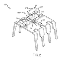
- FIG. 2 is an exploded perspective view of the components depicted in FIG. 1 ;
- FIG. 3 is a cross-sectional view of the components depicted in FIG. 1 ;
- FIG. 4 is a top view of the components depicted in FIG. 1 ;
- FIG. 5 is a flow diagram depicting a coupler manufacturing process in accordance with embodiments of the present disclosure.
- the coupling system 100 may be incorporated into any system which requires current and/or voltage monitoring, but is susceptible to transients.
- the coupling system 100 is rated to operate at about 5 kV or more.
- the coupling system 100 may be incorporated into a coupler and the input of that coupler may directly connected to a 5 kV source without damaging the coupler or its components. Accordingly, the coupling system 100 may be configured to operate in high-voltage or high-current systems.
- the coupling system 100 may be incorporated into a coupler by molding or otherwise encapsulating the contents of the coupling system 100 in a plastic as is known in the chip-manufacturing arts.
- Suitable materials that may be used to mold the coupling system 100 with an and complete the construction of a coupler include, without limitation, plastics or polymers such as polyphthalamide (PPA), silicone, epoxy, any other insulating material, or combinations thereof.
- the coupling system 100 comprises an input side 104 and an output side 108 separated from one another via a gap.
- the gap between the input side 104 and the output side 108 may be filled with air, gas, liquid, plastic, or any other medium which substantially prevents current from passing directly from the input side 104 to the output side 108 .
- the input side 104 is electrically isolated from the output side 108 .
- the input side 104 may be connected to a circuit whose current and/or voltage is being measured and the output side 108 may be connected to measurement and/or control circuitry.
- Both the input side 104 and output side 108 may be constructed of similar or identical materials. Specifically, the input side 104 and output side 108 and the features of each may be manufactured from a single sheet of metal that is stamped, etched, cut, folded, bent, welded, etc. It should be appreciated that any conductive material may be used for constructing the input side 104 and/or output side 108 , which may collectively be referred to as the leadframe of the coupling system 100 . As some non-limiting examples, the leadframe (e.g., the input side 104 and output side 108 ) may be constructed of metal (e.g. copper, silver, gold, aluminum, etc.), graphite, and/or conductive polymers. It may also be possible that the input side 104 and output side 108 are constructed from different materials.
- metal e.g. copper, silver, gold, aluminum, etc.
- graphite e.g. copper, silver, gold, aluminum, etc.
- conductive polymers e.g. copper, silver, gold, aluminum
- the input side 104 may comprise a first section of the input leadframe 112 a and a second section of the input leadframe 112 b , each of which has a plurality of pins 116 .
- the first and second sections 112 a , 112 b may be co-planar to one another.
- the planar top portion of the first section 112 a may be connected to one or more pins 116 via a combination of a joint 124 and taper 120 .
- a gap 128 may reside between most of the first section 112 a and most of the second section 112 b.
- the pins 116 , taper 120 , and shoulder 124 may be collectively referred to as leads.
- leads may comprise any type of known, standardized, or yet-to-be developed configuration such as J leads, SOJ leads, gullwing, reverse gullwing, etc.
- the leads and specifically the pins 116 may be configured to extend away from the first and second sections 112 a , 112 b .
- the joint 124 between the section 112 a , 112 b and a pin 116 may correspond to the feature of the input side 104 where the lead diverges from the plane defined by the sections 112 a , 112 b .
- the taper 120 of the lead corresponds to the feature where the lead decreases is size and specifically decreases is cross-sectional area to a size sufficient to be inserted into a Printed Circuit Board (PCB) input or the like.
- PCB Printed Circuit Board
- the output side 108 may also comprise a plurality of leads that are similar or identical to the leads of the input side 104 .
- each lead of the output side 108 may comprise a pin 136 , a taper 140 , and a joint 144 .
- the output side 108 may differ from the input side 104 in that the output side 108 may comprise a plurality of sections 132 a , 132 b , 132 c , 132 d , where each section has a dedicated lead.
- the output side 108 comprises four leads as is depicted in FIG. 1
- the output side 108 would comprise four sections 132 a , 132 b , 132 c , 132 d .
- the coupling system 100 may comprise a greater or lesser number of leads than those depicted. Specifically, the coupling system 100 depicted herein is intended for use as an 8-pin coupler. Embodiments of the present disclosure contemplate a coupling system 100 having 2 pins, 4 pins, 6 pins, 10 pins, 12 pins, or any other number of pins, whether odd or even.
- a 4-pin coupler would likely comprise a coupling system 100 with two input pins 116 and two output pins 136 .
- One of the input pins 116 would be connected to the first section 112 a and the other of the input pits 116 would be connected to the second section 112 b .
- the output side 108 would only comprise a first section 132 a and a second section 132 b , each having their own dedicated pin 136 .
- the sections 132 a , 132 b , 132 c , 132 d of the output side 108 may be co-planar with the sections 112 a , 112 b of the input side 104 .
- Each section of the output side 108 may be physically and electrically separated from one another in addition to being physically and electrically separated from the input side 104 .
- the relative positions of the input side 104 and output side 108 may be fixed by molding or encapsulating the leadframe in a plastic material. The plastic material may serve the secondary purpose of further electrically insulating the input side 104 from the output side 108 as well as electrically insulating each of the sections 132 a - d of the output side 108 .
- the coupling system 100 may further comprise a sensor assembly 148 that provide a link between the input side 104 and output side 108 .
- the sensor assembly 148 may be configured to detect magnetic fluxes, fields, or the like, created at the input side 104 , convert the magnetic fluxes, fields, etc., into an electrical signal or electrical output and transfer the electrical signal or electrical output to the output side 108 via one or more conductive mechanisms.
- current may be configured to flow in a predetermined pattern through the input side 104 .
- the input side 104 may be constructed to force the current to flow in a path according to arrow 220 .
- the amount of current which flows through the input side 104 may be anywhere between about 1 A and 150 A.
- the sensor assembly 148 may be configured to convert the amount of current flowing through the input side 104 into smaller current amounts (e.g., current on the order of micro-amps or milli-amps).
- the input side 104 since the input side 104 is configured to force the current flowing therethrough to flow in a curved or circular pattern, the input side 104 causes the flowing current to create a magnetic field as described by the Biot-Savart law or Ampere's law. This magnetic field is detected by the sensor assembly 148 and converted into an electrical signal (analog or digital) that has a current which is substantially less than the current flowing through the input side 104 .
- the input side 104 is configured with a notch 224 at the terminus of the gap 128 .
- the notch 124 may comprise a larger width than the gap 128 which causes the current to follow a non-linear path when flowing from the first section 112 a to the second section 112 b .
- a current-directing feature 228 may be located adjacent to the notch 224 and the current-directing feature 228 may be responsible for carrying current from the first section 112 a to the second section 112 b .
- the current-directing feature 228 may be co-planar with the first and second sections 112 a , 112 b , but may be positioned above the ends of the sections (e.g., further away from the leads of the input side 104 than the ends of the sections 112 a , 112 b ). Such a configuration of the input side 104 may enable the current flowing through the input side 104 to create a magnetic field that is strong enough to be detected by the sensor assembly 148 .
- the sensor assembly 148 is shown to include a number of component parts that enable the sensor assembly 148 to detect a magnetic field and convert the detected magnetic field into an electrical signal that can be transferred to the output side 108 .
- the sensor assembly 148 may comprise a sensor carrier 204 , a sensor element 208 , one or more contacts 212 , and an insulator 216 .
- the sensor carrier 204 may correspond to any substrate made of plastic, ceramic, etc. and the sensor element 208 may correspond to any type of sensor or collection of sensors that is capable of sensing a magnetic field and producing a voltage/current that is proportional to the sensed magnetic field strength.
- the sensor element 208 or the entirety of the sensor carrier 204 and sensor element 208 can be miniaturized into a silicon-based semiconductor element.
- a suitable type of sensor element 208 that may be employed is a hall-effect sensor or hall-sensing silicon Integrated Circuit (IC) chip. Examples of suitable sensor elements 208 and/or sensor assemblies 148 are described in further detail in U.S. Pat. Nos. 7,772,661; 7,042,208; 6,879,145; 5,572,058; 4,931,719; and 4,875,011, each of which are hereby incorporated herein by reference in their entirety.
- the sensor assembly 148 may be positioned adjacent, above, or on the leadframe of the input side 104 .
- the sensor assembly 148 is mounted or placed on the first section 112 a , the second section 112 b , and the current-directing feature 228 .
- the insulator 216 of the sensor assembly 148 may comprise a first major surface and an opposing second major surface. The first major surface of the insulator 216 may be placed on the input side 104 and the second major surface of the insulator 216 may be located adjacent to the sensor carrier 204 .
- the insulator 216 is used to enable the coupling system 100 to operate in connection with high input voltages at the input side 104 .
- the insulator 216 may be constructed of any non-conducting material such as polyimide, PPA, or any other type of polymer.
- the insulator 216 provides a physical separation between the current conductor (e.g., the leadframe of the input side 104 ) and the silicon (e.g., the sensor carrier 204 and/or sensor element 208 ).
- the insulator 216 is a layer that may be used to provide the high-voltage isolation between the sensor carrier 204 and/or sensor element 208 and the current flowing through the leadframe.
- the insulator 216 may also operate as an adhesive layer to attach the sensor carrier 204 and/or sensor element 208 onto the leadframe 104 of the input side 104 .
- the overall construction of the coupling system 100 and specifically the sensor assembly 148 may be designed to avoid electrically bridging the input side 104 to the output side 108 , as this will compromise the internal creepage, thereby resulting in a high-voltage failure of the coupling system 100 .
- the thickness of the insulator 216 may be about 2 mils or greater. Where the surface area of the insulator 216 coincides with the surface area of the sensor carrier 204 , the thickness of the insulator 216 may be 3 mils or greater to achieve a 5 kV rating for the coupling system 100 . It should be appreciated that even larger thicknesses of an insulator 216 may be employed, but would result in an increased size of the coupling system 100 . It may be possible that the thickness of the insulator 216 is larger than the thickness of the sensor carrier 204 .
- the sensor assembly 148 may overhang or extend further than the leadframe of the input side 104 .
- a leadframe isolation gap 308 may be defined as the minimum distance between the input side 104 and the output side 108 .
- the sensor assembly 148 may be positioned on the input side 104 so as to hang over or partially cover some of the leadframe isolation gap 308 .
- the minimum distance between the leadframe assembly 148 and the output side 108 may be referred to as a sensor-output gap 312 , which may be smaller than the leadframe isolation gap 308 .
- the sensor-output gap 312 may have a dimension of at least about 10 mils to achieve a 5 kV rating for the coupling system 100 .
- FIG. 3 also depicts a wire 304 that may be used to carry current from a contact 212 of the sensor assembly 148 to an output section 132 a , 132 b , 132 c , 132 d .
- the wire 304 may be constructed of any known type of conductive material or collection of conductive materials.
- the sensor assembly 148 has four contacts 212 , where each contact may be connected to a different output section 132 a - d by a different piece of wire 304 . It should be noted that the number of contacts 212 does not necessarily have to equal the number of output sections 132 . There may be a greater number of contacts 212 than output sections 132 or vice versa. Likewise, not every contact 212 has to be connected to an output section 132 or vice versa.
- one or more of the output sections 132 a - d may comprise an arm 404 or similar feature which extends toward the contacts 212 of the sensor assembly 148 .
- the arm 404 on the output section 132 the amount of wire 404 that is required to connect the contact 212 to the output section 132 can be reduced, thereby reducing the likelihood of failure by virtue of the wire becoming broken or disconnected.
- the relative position of the sensor element 208 and the notch 224 can also be seen in further detail in FIG. 4 . Specifically, it may be desirable to position the sensor element 208 directly above the notch 224 or at some location where the magnetic field produced by the current flowing through the current-directing element 228 is the strongest. By positioning the sensor element 208 at such a location, the accuracy of the coupling system 100 can be increased and/or a less sensitive sensor element 208 can be employed, thereby resulting in a most cost-effective coupling system 100 .
- both the input side 104 and output side 108 of the leadframe may be constructed simultaneously from a single sheet of metal.
- the insulator 216 is positioned relative to the current-directing feature 228 or some other component of the input side 104 (step 508 ).
- the sensor element 208 and/or sensor carrier 204 may then be positioned on the insulator 216 such that the sensor element 208 is at an optimal position for detecting magnetic fields produced by current flowing through the current-directing feature 228 (step 512 ). It should be noted that steps 508 and 512 may be performed simultaneously.
- the sensor assembly 148 may be electrically connected to the output side 108 via one or more wires 304 and then the entire coupling system 100 may be molded or otherwise have the relative positions of the component parts of the coupling system 100 fixed.
- the sensor assembly 148 may be secured to the leadframe and the wires connecting the sensor assembly 148 to the output side 108 of the leadframe may be encapsulated or molded in a plastic or epoxy (step 516 ). Any further steps required to complete the construction of the coupler may then be taken such as bending the leads of the leadframe, removing excess plastic from the mold which now encases the leadframe and sensor assembly 148 , and so on (step 520 ).
Abstract
Description
Claims (20)
Priority Applications (2)
| Application Number | Priority Date | Filing Date | Title |
|---|---|---|---|
| US13/353,494 US9000761B2 (en) | 2012-01-19 | 2012-01-19 | Hall-effect sensor isolator |
| TW102102090A TW201341828A (en) | 2012-01-19 | 2013-01-18 | Hall-effect sensor isolator |
Applications Claiming Priority (1)
| Application Number | Priority Date | Filing Date | Title |
|---|---|---|---|
| US13/353,494 US9000761B2 (en) | 2012-01-19 | 2012-01-19 | Hall-effect sensor isolator |
Publications (2)
| Publication Number | Publication Date |
|---|---|
| US20130187644A1 US20130187644A1 (en) | 2013-07-25 |
| US9000761B2 true US9000761B2 (en) | 2015-04-07 |
Family
ID=48796709
Family Applications (1)
| Application Number | Title | Priority Date | Filing Date |
|---|---|---|---|
| US13/353,494 Active 2032-10-07 US9000761B2 (en) | 2012-01-19 | 2012-01-19 | Hall-effect sensor isolator |
Country Status (2)
| Country | Link |
|---|---|
| US (1) | US9000761B2 (en) |
| TW (1) | TW201341828A (en) |
Cited By (3)
| Publication number | Priority date | Publication date | Assignee | Title |
|---|---|---|---|---|
| US20170222131A1 (en) * | 2016-01-29 | 2017-08-03 | Avago Technologies General Ip (Singapore) Pte. Ltd. | Hall-effect sensor isolator |
| US20180267112A1 (en) * | 2017-03-14 | 2018-09-20 | Ablic Inc. | Magnetic sensor circuit, test method for the same, and manufacturing method for a semiconductor device having a magnetic sensor circuit |
| US11073572B2 (en) | 2019-01-17 | 2021-07-27 | Infineon Technologies Ag | Current sensor device with a routable molded lead frame |
Families Citing this family (4)
| Publication number | Priority date | Publication date | Assignee | Title |
|---|---|---|---|---|
| JP6505505B2 (en) * | 2015-05-27 | 2019-04-24 | 旭化成エレクトロニクス株式会社 | Current sensor |
| CN111668365A (en) * | 2020-06-11 | 2020-09-15 | 苏州纳芯微电子股份有限公司 | Isolation structure applied to current sensor and current sensor |
| CN112775035A (en) * | 2021-01-22 | 2021-05-11 | 福州派利德电子科技有限公司 | High-voltage testing device of optocoupler testing separator and working method thereof |
| JP7328429B1 (en) | 2022-10-04 | 2023-08-16 | 旭化成エレクトロニクス株式会社 | current sensor |
Citations (21)
| Publication number | Priority date | Publication date | Assignee | Title |
|---|---|---|---|---|
| US4616188A (en) | 1985-06-20 | 1986-10-07 | Burr-Brown Corporation | Hall effect isolation amplifier |
| US4875011A (en) | 1986-03-07 | 1989-10-17 | Seiko Instruments Inc. | Magnetic sensor using integrated silicon Hall effect elements formed on the (100) plane of a silicon substrate |
| US4931719A (en) | 1988-08-05 | 1990-06-05 | Mitsubishi Denki Kabushiki Kaisha | Hall-effect sensor arrangement |
| US5572058A (en) | 1995-07-17 | 1996-11-05 | Honeywell Inc. | Hall effect device formed in an epitaxial layer of silicon for sensing magnetic fields parallel to the epitaxial layer |
| US6356068B1 (en) * | 1997-09-15 | 2002-03-12 | Ams International Ag | Current monitor system and a method for manufacturing it |
| US6373241B1 (en) | 1997-09-10 | 2002-04-16 | Robert Bosch Gmbh | Sensor device having a magnetic field sensor integrated with an electronic control circuit |
| US20050030018A1 (en) * | 2001-11-01 | 2005-02-10 | Koji Shibahara | Current sensor and current sensor manufacturing method |
| US6879145B1 (en) | 2002-02-15 | 2005-04-12 | Larry L. Harris | Voltage isolation buffer with hall effect magnetic field sensor |
| US20050248336A1 (en) * | 2003-08-26 | 2005-11-10 | Nirmal Sharma | Current sensor |
| US20080136399A1 (en) * | 2006-12-12 | 2008-06-12 | Alfano Donald E | Current sensor |
| US20080143329A1 (en) * | 2006-12-14 | 2008-06-19 | Denso Corporation | Semiconductor integrated circuit for detecting magnetic field |
| US20080297138A1 (en) * | 2003-08-26 | 2008-12-04 | Taylor William P | Current sensor |
| US20100045282A1 (en) | 2006-11-30 | 2010-02-25 | Ichiro Shibasaki | Thin film lamination, thin film magnetic sensor using the thin film lamination and method for manufacturing the thin film lamination |
| US7746056B2 (en) | 2003-02-11 | 2010-06-29 | Allegro Microsystems, Inc. | Integrated sensor |
| US7772661B2 (en) | 2008-07-23 | 2010-08-10 | Honeywell International Inc. | Hall-effect magnetic sensors with improved magnetic responsivity and methods for manufacturing the same |
| US7816905B2 (en) | 2008-06-02 | 2010-10-19 | Allegro Microsystems, Inc. | Arrangements for a current sensing circuit and integrated current sensor |
| US20110248711A1 (en) * | 2010-04-08 | 2011-10-13 | Infineon Technologies Ag | Magnetic field current sensors |
| US20120001649A1 (en) * | 2010-06-30 | 2012-01-05 | Linear Technology Corporation | Leadframe current sensor |
| US20130015843A1 (en) * | 2011-07-13 | 2013-01-17 | Allegro Microsystems, Inc. | Current sensor with calibration for a current divider configuration |
| US20130020660A1 (en) * | 2011-07-22 | 2013-01-24 | Allegro Microsystems, Inc. | Reinforced Isolation for Current Sensor with Magnetic Field Transducer |
| US20130049746A1 (en) * | 2011-08-30 | 2013-02-28 | Infineon Technologies Ag | Semiconductor Chip Package and Method |
-
2012
- 2012-01-19 US US13/353,494 patent/US9000761B2/en active Active
-
2013
- 2013-01-18 TW TW102102090A patent/TW201341828A/en unknown
Patent Citations (22)
| Publication number | Priority date | Publication date | Assignee | Title |
|---|---|---|---|---|
| US4616188A (en) | 1985-06-20 | 1986-10-07 | Burr-Brown Corporation | Hall effect isolation amplifier |
| US4875011A (en) | 1986-03-07 | 1989-10-17 | Seiko Instruments Inc. | Magnetic sensor using integrated silicon Hall effect elements formed on the (100) plane of a silicon substrate |
| US4931719A (en) | 1988-08-05 | 1990-06-05 | Mitsubishi Denki Kabushiki Kaisha | Hall-effect sensor arrangement |
| US5572058A (en) | 1995-07-17 | 1996-11-05 | Honeywell Inc. | Hall effect device formed in an epitaxial layer of silicon for sensing magnetic fields parallel to the epitaxial layer |
| US6373241B1 (en) | 1997-09-10 | 2002-04-16 | Robert Bosch Gmbh | Sensor device having a magnetic field sensor integrated with an electronic control circuit |
| US6356068B1 (en) * | 1997-09-15 | 2002-03-12 | Ams International Ag | Current monitor system and a method for manufacturing it |
| US20050030018A1 (en) * | 2001-11-01 | 2005-02-10 | Koji Shibahara | Current sensor and current sensor manufacturing method |
| US6879145B1 (en) | 2002-02-15 | 2005-04-12 | Larry L. Harris | Voltage isolation buffer with hall effect magnetic field sensor |
| US7042208B1 (en) | 2002-02-15 | 2006-05-09 | Harris Larry L | Voltage isolation buffer with AC coupled and DC coupled hall effect magnetic field sensors |
| US7746056B2 (en) | 2003-02-11 | 2010-06-29 | Allegro Microsystems, Inc. | Integrated sensor |
| US20050248336A1 (en) * | 2003-08-26 | 2005-11-10 | Nirmal Sharma | Current sensor |
| US20080297138A1 (en) * | 2003-08-26 | 2008-12-04 | Taylor William P | Current sensor |
| US20100045282A1 (en) | 2006-11-30 | 2010-02-25 | Ichiro Shibasaki | Thin film lamination, thin film magnetic sensor using the thin film lamination and method for manufacturing the thin film lamination |
| US20080136399A1 (en) * | 2006-12-12 | 2008-06-12 | Alfano Donald E | Current sensor |
| US20080143329A1 (en) * | 2006-12-14 | 2008-06-19 | Denso Corporation | Semiconductor integrated circuit for detecting magnetic field |
| US7816905B2 (en) | 2008-06-02 | 2010-10-19 | Allegro Microsystems, Inc. | Arrangements for a current sensing circuit and integrated current sensor |
| US7772661B2 (en) | 2008-07-23 | 2010-08-10 | Honeywell International Inc. | Hall-effect magnetic sensors with improved magnetic responsivity and methods for manufacturing the same |
| US20110248711A1 (en) * | 2010-04-08 | 2011-10-13 | Infineon Technologies Ag | Magnetic field current sensors |
| US20120001649A1 (en) * | 2010-06-30 | 2012-01-05 | Linear Technology Corporation | Leadframe current sensor |
| US20130015843A1 (en) * | 2011-07-13 | 2013-01-17 | Allegro Microsystems, Inc. | Current sensor with calibration for a current divider configuration |
| US20130020660A1 (en) * | 2011-07-22 | 2013-01-24 | Allegro Microsystems, Inc. | Reinforced Isolation for Current Sensor with Magnetic Field Transducer |
| US20130049746A1 (en) * | 2011-08-30 | 2013-02-28 | Infineon Technologies Ag | Semiconductor Chip Package and Method |
Cited By (5)
| Publication number | Priority date | Publication date | Assignee | Title |
|---|---|---|---|---|
| US20170222131A1 (en) * | 2016-01-29 | 2017-08-03 | Avago Technologies General Ip (Singapore) Pte. Ltd. | Hall-effect sensor isolator |
| US10283699B2 (en) * | 2016-01-29 | 2019-05-07 | Avago Technologies International Sales Pte. Limited | Hall-effect sensor isolator |
| US20180267112A1 (en) * | 2017-03-14 | 2018-09-20 | Ablic Inc. | Magnetic sensor circuit, test method for the same, and manufacturing method for a semiconductor device having a magnetic sensor circuit |
| US10641841B2 (en) * | 2017-03-14 | 2020-05-05 | Ablic Inc. | Magnetic sensor circuit, test method for the same, and manufacturing method for a semiconductor device having a magnetic sensor circuit |
| US11073572B2 (en) | 2019-01-17 | 2021-07-27 | Infineon Technologies Ag | Current sensor device with a routable molded lead frame |
Also Published As
| Publication number | Publication date |
|---|---|
| TW201341828A (en) | 2013-10-16 |
| US20130187644A1 (en) | 2013-07-25 |
Similar Documents
| Publication | Publication Date | Title |
|---|---|---|
| US9000761B2 (en) | Hall-effect sensor isolator | |
| US6545456B1 (en) | Hall effect current sensor package for sensing electrical current in an electrical conductor | |
| US10283699B2 (en) | Hall-effect sensor isolator | |
| US10215781B2 (en) | Current sensor | |
| JP6467696B2 (en) | Current measuring device | |
| US9564423B2 (en) | Power package with integrated magnetic field sensor | |
| CN108155157B (en) | Integrated circuit package including lead frame | |
| US11112435B2 (en) | Current transducer with integrated primary conductor | |
| US8587298B2 (en) | Current measuring device by means of magnetically sensitive sensor for a power electronics system | |
| CN110854104B (en) | Current sensor package | |
| US9231118B2 (en) | Chip package with isolated pin, isolated pad or isolated chip carrier and method of making the same | |
| CN106461705A (en) | Current sensor | |
| CN102565506A (en) | Current sensor | |
| JP6505505B2 (en) | Current sensor | |
| CN109791926A (en) | Semiconductor device | |
| US11231445B2 (en) | Sensor chip | |
| CN104078194B (en) | Magnetic devices and its assemble method with integrated current sensing element | |
| US20140306732A1 (en) | Detection of defective electrical connections | |
| US11296073B2 (en) | Semiconductor device | |
| JP6314010B2 (en) | Current sensor | |
| CN107861056A (en) | It is determined that the method and system and power switch circuit of the electric current for passing through power switch | |
| JP2010197346A (en) | Power semiconductor module and power converter using power semiconductor module | |
| US9504143B2 (en) | Electrical circuit | |
| CN117289012B (en) | Dual-current input/output, dual-isolation current sensor and current detection method | |
| US20230163056A1 (en) | Semiconductor module |
Legal Events
| Date | Code | Title | Description |
|---|---|---|---|
| AS | Assignment |
Owner name: AVAGO TECHNOLOGIES ECBU IP (SINGAPORE) PTE. LTD., Free format text: ASSIGNMENT OF ASSIGNORS INTEREST;ASSIGNORS:TAY, GARY;HO, DOMINIQUE;SHIE, MENG YONG;SIGNING DATES FROM 20120117 TO 20120118;REEL/FRAME:027562/0535 |
|
| AS | Assignment |
Owner name: AVAGO TECHNOLOGIES GENERAL IP (SINGAPORE) PTE. LTD., SINGAPORE Free format text: MERGER;ASSIGNOR:AVAGO TECHNOLOGIES ECBU IP (SINGAPORE) PTE. LTD.;REEL/FRAME:030369/0496 Effective date: 20121030 Owner name: AVAGO TECHNOLOGIES GENERAL IP (SINGAPORE) PTE. LTD Free format text: MERGER;ASSIGNOR:AVAGO TECHNOLOGIES ECBU IP (SINGAPORE) PTE. LTD.;REEL/FRAME:030369/0496 Effective date: 20121030 |
|
| AS | Assignment |
Owner name: DEUTSCHE BANK AG NEW YORK BRANCH, AS COLLATERAL AGENT, NEW YORK Free format text: PATENT SECURITY AGREEMENT;ASSIGNOR:AVAGO TECHNOLOGIES GENERAL IP (SINGAPORE) PTE. LTD.;REEL/FRAME:032851/0001 Effective date: 20140506 Owner name: DEUTSCHE BANK AG NEW YORK BRANCH, AS COLLATERAL AG Free format text: PATENT SECURITY AGREEMENT;ASSIGNOR:AVAGO TECHNOLOGIES GENERAL IP (SINGAPORE) PTE. LTD.;REEL/FRAME:032851/0001 Effective date: 20140506 |
|
| STCF | Information on status: patent grant |
Free format text: PATENTED CASE |
|
| AS | Assignment |
Owner name: AVAGO TECHNOLOGIES GENERAL IP (SINGAPORE) PTE. LTD., SINGAPORE Free format text: TERMINATION AND RELEASE OF SECURITY INTEREST IN PATENT RIGHTS (RELEASES RF 032851-0001);ASSIGNOR:DEUTSCHE BANK AG NEW YORK BRANCH, AS COLLATERAL AGENT;REEL/FRAME:037689/0001 Effective date: 20160201 Owner name: AVAGO TECHNOLOGIES GENERAL IP (SINGAPORE) PTE. LTD Free format text: TERMINATION AND RELEASE OF SECURITY INTEREST IN PATENT RIGHTS (RELEASES RF 032851-0001);ASSIGNOR:DEUTSCHE BANK AG NEW YORK BRANCH, AS COLLATERAL AGENT;REEL/FRAME:037689/0001 Effective date: 20160201 |
|
| AS | Assignment |
Owner name: BANK OF AMERICA, N.A., AS COLLATERAL AGENT, NORTH CAROLINA Free format text: PATENT SECURITY AGREEMENT;ASSIGNOR:AVAGO TECHNOLOGIES GENERAL IP (SINGAPORE) PTE. LTD.;REEL/FRAME:037808/0001 Effective date: 20160201 Owner name: BANK OF AMERICA, N.A., AS COLLATERAL AGENT, NORTH Free format text: PATENT SECURITY AGREEMENT;ASSIGNOR:AVAGO TECHNOLOGIES GENERAL IP (SINGAPORE) PTE. LTD.;REEL/FRAME:037808/0001 Effective date: 20160201 |
|
| AS | Assignment |
Owner name: AVAGO TECHNOLOGIES GENERAL IP (SINGAPORE) PTE. LTD., SINGAPORE Free format text: TERMINATION AND RELEASE OF SECURITY INTEREST IN PATENTS;ASSIGNOR:BANK OF AMERICA, N.A., AS COLLATERAL AGENT;REEL/FRAME:041710/0001 Effective date: 20170119 Owner name: AVAGO TECHNOLOGIES GENERAL IP (SINGAPORE) PTE. LTD Free format text: TERMINATION AND RELEASE OF SECURITY INTEREST IN PATENTS;ASSIGNOR:BANK OF AMERICA, N.A., AS COLLATERAL AGENT;REEL/FRAME:041710/0001 Effective date: 20170119 |
|
| MAFP | Maintenance fee payment |
Free format text: PAYMENT OF MAINTENANCE FEE, 4TH YEAR, LARGE ENTITY (ORIGINAL EVENT CODE: M1551); ENTITY STATUS OF PATENT OWNER: LARGE ENTITY Year of fee payment: 4 |
|
| AS | Assignment |
Owner name: AVAGO TECHNOLOGIES INTERNATIONAL SALES PTE. LIMITE Free format text: MERGER;ASSIGNOR:AVAGO TECHNOLOGIES GENERAL IP (SINGAPORE) PTE. LTD.;REEL/FRAME:047422/0464 Effective date: 20180509 |
|
| AS | Assignment |
Owner name: AVAGO TECHNOLOGIES INTERNATIONAL SALES PTE. LIMITE Free format text: CORRECTIVE ASSIGNMENT TO CORRECT THE EXECUTION DATE PREVIOUSLY RECORDED AT REEL: 047422 FRAME: 0464. ASSIGNOR(S) HEREBY CONFIRMS THE MERGER;ASSIGNOR:AVAGO TECHNOLOGIES GENERAL IP (SINGAPORE) PTE. LTD.;REEL/FRAME:048883/0702 Effective date: 20180905 |
|
| MAFP | Maintenance fee payment |
Free format text: PAYMENT OF MAINTENANCE FEE, 8TH YEAR, LARGE ENTITY (ORIGINAL EVENT CODE: M1552); ENTITY STATUS OF PATENT OWNER: LARGE ENTITY Year of fee payment: 8 |