EP1890239B1 - Speichersteuerung und Verfahren zur Speichersteuerung - Google Patents
Speichersteuerung und Verfahren zur Speichersteuerung Download PDFInfo
- Publication number
- EP1890239B1 EP1890239B1 EP07106725A EP07106725A EP1890239B1 EP 1890239 B1 EP1890239 B1 EP 1890239B1 EP 07106725 A EP07106725 A EP 07106725A EP 07106725 A EP07106725 A EP 07106725A EP 1890239 B1 EP1890239 B1 EP 1890239B1
- Authority
- EP
- European Patent Office
- Prior art keywords
- error
- data
- memory
- address line
- occurred
- Prior art date
- Legal status (The legal status is an assumption and is not a legal conclusion. Google has not performed a legal analysis and makes no representation as to the accuracy of the status listed.)
- Ceased
Links
Images



Classifications
-
- G—PHYSICS
- G06—COMPUTING OR CALCULATING; COUNTING
- G06F—ELECTRIC DIGITAL DATA PROCESSING
- G06F13/00—Interconnection of, or transfer of information or other signals between, memories, input/output devices or central processing units
- G06F13/14—Handling requests for interconnection or transfer
- G06F13/16—Handling requests for interconnection or transfer for access to memory bus
- G06F13/1668—Details of memory controller
- G06F13/1684—Details of memory controller using multiple buses
-
- G—PHYSICS
- G06—COMPUTING OR CALCULATING; COUNTING
- G06F—ELECTRIC DIGITAL DATA PROCESSING
- G06F11/00—Error detection; Error correction; Monitoring
-
- G—PHYSICS
- G06—COMPUTING OR CALCULATING; COUNTING
- G06F—ELECTRIC DIGITAL DATA PROCESSING
- G06F11/00—Error detection; Error correction; Monitoring
- G06F11/07—Responding to the occurrence of a fault, e.g. fault tolerance
- G06F11/08—Error detection or correction by redundancy in data representation, e.g. by using checking codes
- G06F11/10—Adding special bits or symbols to the coded information, e.g. parity check, casting out 9's or 11's
- G06F11/1008—Adding special bits or symbols to the coded information, e.g. parity check, casting out 9's or 11's in individual solid state devices
- G06F11/1044—Adding special bits or symbols to the coded information, e.g. parity check, casting out 9's or 11's in individual solid state devices with specific ECC/EDC distribution
-
- G—PHYSICS
- G06—COMPUTING OR CALCULATING; COUNTING
- G06F—ELECTRIC DIGITAL DATA PROCESSING
- G06F11/00—Error detection; Error correction; Monitoring
- G06F11/07—Responding to the occurrence of a fault, e.g. fault tolerance
- G06F11/16—Error detection or correction of the data by redundancy in hardware
- G06F11/1666—Error detection or correction of the data by redundancy in hardware where the redundant component is memory or memory area
-
- G—PHYSICS
- G06—COMPUTING OR CALCULATING; COUNTING
- G06F—ELECTRIC DIGITAL DATA PROCESSING
- G06F12/00—Accessing, addressing or allocating within memory systems or architectures
- G06F12/16—Protection against loss of memory contents
-
- G—PHYSICS
- G11—INFORMATION STORAGE
- G11C—STATIC STORES
- G11C29/00—Checking stores for correct operation ; Subsequent repair; Testing stores during standby or offline operation
- G11C29/04—Detection or location of defective memory elements, e.g. cell constructio details, timing of test signals
- G11C29/08—Functional testing, e.g. testing during refresh, power-on self testing [POST] or distributed testing
- G11C29/12—Built-in arrangements for testing, e.g. built-in self testing [BIST] or interconnection details
- G11C29/38—Response verification devices
- G11C29/42—Response verification devices using error correcting codes [ECC] or parity check
-
- G—PHYSICS
- G11—INFORMATION STORAGE
- G11C—STATIC STORES
- G11C29/00—Checking stores for correct operation ; Subsequent repair; Testing stores during standby or offline operation
- G11C29/70—Masking faults in memories by using spares or by reconfiguring
- G11C29/74—Masking faults in memories by using spares or by reconfiguring using duplex memories, i.e. using dual copies
-
- G—PHYSICS
- G11—INFORMATION STORAGE
- G11C—STATIC STORES
- G11C29/00—Checking stores for correct operation ; Subsequent repair; Testing stores during standby or offline operation
- G11C29/70—Masking faults in memories by using spares or by reconfiguring
- G11C29/78—Masking faults in memories by using spares or by reconfiguring using programmable devices
- G11C29/84—Masking faults in memories by using spares or by reconfiguring using programmable devices with improved access time or stability
- G11C29/846—Masking faults in memories by using spares or by reconfiguring using programmable devices with improved access time or stability by choosing redundant lines at an output stage
-
- G—PHYSICS
- G11—INFORMATION STORAGE
- G11C—STATIC STORES
- G11C29/00—Checking stores for correct operation ; Subsequent repair; Testing stores during standby or offline operation
- G11C29/04—Detection or location of defective memory elements, e.g. cell constructio details, timing of test signals
- G11C2029/0409—Online test
-
- G—PHYSICS
- G11—INFORMATION STORAGE
- G11C—STATIC STORES
- G11C29/00—Checking stores for correct operation ; Subsequent repair; Testing stores during standby or offline operation
- G11C29/04—Detection or location of defective memory elements, e.g. cell constructio details, timing of test signals
- G11C2029/0411—Online error correction
-
- G—PHYSICS
- G11—INFORMATION STORAGE
- G11C—STATIC STORES
- G11C5/00—Details of stores covered by group G11C11/00
- G11C5/02—Disposition of storage elements, e.g. in the form of a matrix array
- G11C5/04—Supports for storage elements, e.g. memory modules; Mounting or fixing of storage elements on such supports
Definitions
- This invention relates to a technology for controlling a memory in a dual memory system.
- a technology is conventionally disclosed that enhances reliability in a data processing device and the like by employing a redundant memory system that uses, for example, a DIMM (Dual Inline Memory Module) in a data processing device.
- DIMM Dual Inline Memory Module
- a technology that enhances reliability in a redundant memory system by managing trouble information in an address unit at the time of an initial diagnosis of a redundant memory system and, even when a fixing trouble of equal to or more than 2 bits is detected at one line of redundant memory, performing changing to the other line to efficiently utilize a capability of recovering.
- reliability of a redundant memory system is improved by indicating only an address of the corresponding memory as invalid or valid, outputting an invalid signal concerning the address to disable a comparison circuit, and indicating that an address is valid and use of data in memory that has an address in which a parity error is not detected.
- the above conventional technology is a technology to enhance reliability in a redundant memory system based on trouble information in initial diagnosis of a redundant memory system.
- the technology has a problem that it is impossible to deal with trouble information that is informed in activating a system.
- An error on an address line of a DIMM that is a redundant memory system is not supported in the above conventional technology. Therefore, when an error occurs on an address line, it cannot be recognized and then it is even hazardous to use data of a wrong address.
- ECC Error Correcting Code
- a technology of constituting one ECC (Error Correcting Code) error check unit through a plurality of DIMMs (for example, two DIMMs) to avoid the hazard there is a possibility that coincidence of ECCs that occurs at a certain probability causes error data. Occurrence of error data through accidental coincidence of ECCs, when a line of redundant memory is changed to recover an error, makes it difficult to determine which line to select, thereby causing a problem that a system down may occur.
- the document GB 2 220 091 discloses a memory error protection system to be used with a number of parallel memory banks (M1, M2) each containing a number of DRAM devices. It includes a memory control unit; a pair of parity generators and checkers (GC1, GC2) which are associated with respective memory banks; a pair of bus isolators (B11, B12); and a data comparator (DC). Errors between bits of information stored in corresponding memory devices of the memory banks are detected and switching between memory banks can be achieved in order to ensure that only the correct data is output onto a memory data highway (MH).
- the system is also capable of selecting appropriate levels of protection and switching between them as required.
- the system can also be used to detect address violations, un-initialised variables or particular variable values (or ranges).
- a memory controller controls a memory in a system in which an error checking unit of data is formed with a plurality of memories each of which is a dual memory having an independent address line.
- the memory controller includes an estimating unit that estimates, when there is a request for data in the system, whether an error has occurred on the address line based on a result of an error checking for data related to the request; and a control unit that generates, when it is estimated that an error has occurred on the address line, error data of the data related to the request, and controls the memory in such a manner that one line of the dual memory is disabled by switching the data related to the request to generated error data.
- the method includes estimating, when there is a request for data in the system, whether an error has occurred on the address line based on a result of an error checking for data related to the request; generating, when it is estimated that an error has occurred on the address line, error data of the data related to the request; and controlling the memory in such a manner that one line of the dual memory is disabled by switching the data related to the request to generated error data.
- a computer-readable recording medium stores therein a computer program for controlling a memory in a system in which an error checking unit of data is formed with a plurality of memories each of which is a dual memory having an independent address line.
- the computer program causes a computer to execute estimating, when there is a request for data in the system, whether an error has occurred on the address line based on a result of an error checking for data related to the request; generating, when it is estimated that an error has occurred on the address line, error data of the data related to the request; and controlling the memory in such a manner that one line of the dual memory is disabled by switching the data related to the request to generated error data.
- Fig. 1 is a schematic for explaining the outline and characteristic of the memory controller according to a first embodiment of the present invention.
- the memory controller has the outline that an error checking unit of data is constituted of a plurality of memories each of which has an address line and the controller controls memory in a redundant memory system (mirror) and the characteristic that it is possible to prevent a system down by dealing with trouble information in real time and estimating an error on an address line.
- a redundant memory system mirror
- an LDX#1 connected to a DIMM1, an LDX#0 connected to a DIMM0, and an LDX#3 connected to a DIMM3, and an LDX#2 connected to a DIMM2 constitute a mirror
- the DIMM1 and the DIMM0 constitute a data unit
- the LDX#1 connected to the DIMM1 and the LDX#0 connected to the DIMM0 constitute an ECC check unit that is an error checking unit.
- the LDX#1 and the LDX#0 exchange ECC information that each of them has (information for ECC check) to perform ECC check, perform ECC checking with regard to a part of request data respectively, and estimate whether an error occurs on an address line (see (3) shown in Fig. 1 ). More specifically, for example, the LDX#0 creates a syndrome (diagnosis information) that is a result of ECC check about a part of request data and estimates that an error occurs on an address line based on a condition of the error about a part of request data obtained from the syndrome, for example, when most of request data causes an uncorrectable error. When the LDX#0 estimates that an error occurs on an address line, the LDX#1 also estimates that an error occurs on an address line.
- ECC information that each of them has (information for ECC check) to perform ECC check, perform ECC checking with regard to a part of request data respectively, and estimate whether an error occurs on an address line (see (3) shown in Fig. 1 ). More specifically, for example
- the LDX#1 and the LDX#0 When it is estimated that an error occurs on an address line, the LDX#1 and the LDX#0 create error data with regard to a part of request data that each of them manages, and switch a part of request data to error data that each of them generates (see (4) shown in Fig. 1 ).
- the LDX#1 and the LDX#0 output the switched error data to an FLN (comparison circuit) to control not to use data recorded in the DIMM1 and the DIMM0 that constitute one line of a mirror (see (5) shown in Fig. 1 ).
- the FLN compares request data that is input from the LDX#3 and the LDX#2 that constitute the other line of the mirror with data input from the LDX#1 and the LDX#0 (see (6) shown in Fig. 1 ), because the data input from the LDX#1 and the LDX#0 is error data, the data is not employed as targeted comparison.
- the request data input from the LDX#3 and the LDX#2 is output to the CPU1 from which the data is originally requested (see (7) shown in Fig. 1 ).
- the first embodiment it is possible to deal with trouble information such as estimated error information of an address line in real time in the redundant memory system (mirror) and, if error data is caused due to an error on an address line, before comparing data in the FLN (comparison circuit) in the redundant memory system (mirror), to switch to generated error data not to compare, enabling prevention of a system down by estimating an error in an address line, as the above-mentioned main characteristic.
- trouble information such as estimated error information of an address line in real time in the redundant memory system (mirror) and, if error data is caused due to an error on an address line, before comparing data in the FLN (comparison circuit) in the redundant memory system (mirror), to switch to generated error data not to compare, enabling prevention of a system down by estimating an error in an address line, as the above-mentioned main characteristic.
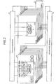
- Fig. 2 is a diagram of a configuration of a system to which the memory controller according to the first embodiment is applied.
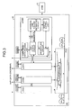
- Fig. 3 is a block diagram of the system board and the memory controller according to the first embodiment.
- the system to which the memory controller according to the first embodiment is applied includes an MMB 10, a GDX (Data Crossbar) 20, a GAC (Address Crossbar) 30, an SB 40, and an IOU (Input/output Unit) 50.
- the MMB 10 is a control device that performs various controls about the GDX 20, GAC 30, SB 40, and IOU 50.
- the GDX 20 is a relay device that communicates data between the SB 40 and the IOU 50.
- the GAC 30 is a relay device that controls relay of a request input from the SB 40 and the IOU 50 and a request response.
- the SB 40 in which DIMMs, LDXs, CPUs, and the like are arranged is a board that controls various information processing.
- the IOU 50 is a board that includes an input output interface of an external device connected from outside.
- the SB 40 has the LDX#3 connected to the DIMM3 and the LDX#2 connected to the DIMM2, and the LDX#1 connected to the DIMM1 and the LDX#0 connected to the DIMM0 arranged to constitute a mirror and includes the CPU and the FLN arranged therein.
- the DIMM is a storing device that stores data and a program necessary for various processing by the CPU.
- the DIMM3 and the DIMM2, and the DIMM1 and the DIMM0 constitute a data unit respectively.
- the LDX is a processor that controls the DIMM based on various information input from the DIMM.
- the CPU is a processor that has an internal memory to store a predetermined control program, a program that prescribes various processing procedures, and required data to execute various processing through them.
- the FLN is a processor that has a circuit that respectively compares data input from each LDX that constitutes a mirror to output data to the CPU.
- the LDX#0 to #3 includes a DIMM-read-data holding unit, an ECC checking circuit, an address-line-failure estimating circuit, a switch control unit, and a UE generating circuit.
- the DIMM-read-data holding unit temporarily holds a part of request data read from the DIMM.
- the ECC checking circuit checks an error based on an ECC with respect to a part of request data held in the DIMM-read-data holding unit and outputs the resulting checking to an address-line-failure estimating circuit.
- An ECC check unit in an ECC check circuit of the LDX#3 and an ECC check circuit of the LDX#2 and an ECC check unit in an ECC check circuit of the LDX#1 and an ECC check circuit of the LDX#0 are constituted respectively.
- the ECC checking circuit that includes an ECC check unit exchanges ECC information (information for ECC checking) to perform error checking based on ECC.
- the address-line-failure estimating circuit estimates whether an error occurs on an address line based on the resulting error checking about a part of request data received from the ECC check circuit. More specifically, for example, the LDX#0 creates a syndrome (diagnosis information) that is the resulting ECC checking about a part of request data and estimates that an error occurs on an address line, for example, when most of the request data causes an uncorrectable error, based on a condition of an error about a part of the request data obtained from the syndrome. When it is estimated that an error occurs on an address line, the signal is output to the switch control unit. When the LDX#0 estimates that an error occurs on an address line, the LDX#1 also estimates that an error occurs on an address line.
- the switch control unit is a processor that controls a switch of request data to error data. More specifically, when a signal that estimates that an error occurs on an address line is input from the address-line-failure estimating circuit, a signal is output to the UE generating circuit to generate error data with regard to a part of request data and switch to error data that generates a part of request data.
- the UE (Uncorrectable Error) generating circuit generates error data that causes an uncorrectable error with regard to request data to switch. More specifically, based on a signal received from the error switch control unit, error data is generated from request data and request data is switched to error data.
- the LDX#1 and the LDX#0 output switched error data to the FLN (comparison circuit) to control not to use data recorded in the DIMM1 and the DIMM0 that constitute one line of a mirror. Error data output from the LDX#1 and the LDX#0 respectively is coupled to become error data about request data.
- the FLN compares request data that is received from the LDX#3 and the LDX#2 that constitute the other line of the mirror with data received from the LDX#1 and the LDX#0, because the data received from the LDX#1 and the LDX#0 is error data, the data is not employed as targeted comparison.
- Request data received from the LDX#3 and the LDX#2 is output where the data is originally requested (for example, CPU).
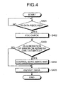
- Fig. 4 is a flowchart for explaining processing of the memory controller according to the first embodiment.
- the LDX#0 temporarily holds it at the DIMM-read-data holding unit.
- the ECC check circuit of the LDX#0 gives an error check, through the ECC, to a part of request data held at the DIMM-read-data holding unit (step S402), the resulting checking is output to the address-line-failure estimating circuit.
- the ECC check circuit exchanges ECC information (information for checking ECC) with another ECC check circuit that constitutes an ECC check unit to perform error checking through ECC.
- the address-line-failure estimating circuit estimates whether an error occurs on an address line based on the resulting error checking about a part of request data input from the ECC check circuit (step S403). More specifically, for example, a syndrome (diagnosis information) that is a resulting ECC checking about a part of request data is created and the address-line-failure estimating circuit estimates that an error occurs on an address line based on a condition of an error about a part of request data obtained from the syndrome, for example when most of the request data causes an uncorrectable error.
- a syndrome diagnosis information
- the address-line-failure estimating circuit When it is estimated that an error occurs on an address line (yes at step S403), the address-line-failure estimating circuit outputs the signal to the switch control unit.
- the switch control unit controls to switch a part of request data to error data (step S404). More specifically, when a signal that estimates that an error occurs on an address line is input from the address-line-failure estimating circuit, error data about a part of request data is created at the UE generating circuit, and a signal to switch to error data that generates a part of request data is output.
- the address-line-failure estimating circuit does not particularly output a signal to the switch control unit when the address-line-failure estimating circuit does not estimate that an error occurs on an address line (no at step S403).
- the LDX#0 outputs the switched error data to the FLN (comparison circuit) to control not to use data recorded in the DIMM0 that constitutes one line of mirror and the LDX#1 also outputs the switched error data to the FLN (comparison circuit) to control not to use data recorded in DIMM1 (step S405).
- whether an error occurs on an address line (a line that transmits a data address of a request) is estimated based on the result (for example, the result of ECC checking) of error checking of request data that is performed when there is a request in the system.
- error data is created with respect to data of the request to switch the data to error data, thereby controlling not to use data of one line of redundant memory.
- an error it is estimated whether an error occurs on an address line based on the result of error checking that is performed about connected memory. For example, a system configuration of controlling one DIMM by one memory controller has a higher capability than a system configuration of controlling two DIMM by one memory controller. Thus, estimation of an error on an address line enables prevention of a system down.
- Estimation of whether an error occurs on an address line is explained based on a condition of an error of request data obtained as the resulting error checking through the ECC check circuit (a degree of how data is damaged) in the first embodiment, however, the present invention is not limited to the first embodiment.
- the number of times when uncorrectable errors occur is obtained in error checking of request data in the ECC check circuit and whether an error occurs on an address line can be estimated based on the obtained number of times.
- Fig. 5 is a block diagram of a system board and a memory controller according to the second embodiment.
- the configuration of the SB and the memory controller according to the second embodiment is fundamentally the same as the configuration of the SB and the memory controller according to the first embodiment except the following description.
- the address-line-failure estimating circuit includes a counter, Decoder, and OPSR.
- the counter is a device that counts the number of times when uncorrectable errors occur that are detected by error checking of the ECC check circuit.
- the Decoder outputs a counter value.
- the OSPR (operation register) receives setting from the MMB 10, estimates that an error occur on an address line, and specifies the counter value to make the switch control unit switch a part of request data to error data. For example, as shown in Fig. 6 , the OSPR has a table to store whether data switching is performed corresponding to the number of times when uncorrectable errors occur to estimate that an error occurs on an address line.
- the address-line-failure estimating circuit determines whether the counter value output from the Decoder exceeds the upper-limit number of times designated by the OPSR. As a result, when the counter value exceeds the upper-limit number of times, the address-line-failure estimating circuit outputs a signal to switch the request data to the error data to the switch control unit.
- the upper-limit number of times can be appropriately altered based on change of setting from the MMB 10.
- the switch control unit When the switch control unit receives a signal from the address-line-failure estimating circuit, it controls to switch request data to error data. More specifically, the switch control unit outputs a signal, to the UE generating circuit, to generate error data with respect to a part of request data and switch to error data that generates a part of request data.
- the table that the OPSR has is only an example.
- a table whose structure is appropriately altered can be generated without being limited to the table that the OPSR has.
- the address-line-failure estimating circuit estimates that a failure occurs on an address line and can make the switch control unit control to switch a part of request data to error data.
- Fig.7 is a flowchart for explaining processing of the memory controller according to the second embodiment.
- the processing of steps S701, S702, and S705 is the same as processing of steps S401, S402, and S405 that are described in the first embodiment shown in Fig. 4 .
- processing of steps S703 and S704 is explained below.
- the address-line-failure estimating circuit estimates whether an error occurs on an address line based on the result of error checking about a part of request data input from the ECC check circuit (step S703). More specifically, whether the counter value output from the Decoder exceeds the upper-limit number of times designated from the OPSR is determined. As a result of the determination, when the counter value exceeds the upper-limit number of times (yes at step S703), the address-line-failure estimating circuit estimates that an error occurs on an address line and outputs a signal to the switch control unit to switch request data to error data. On the other hand, the address-line-failure estimating circuit, when the counter value does not exceed the upper-limit number of times (no at step S703), does not particularly output a signal to the switch control unit.
- the switch control unit when a signal is input from the address-line-failure estimating circuit, controls to switch request data to error data (step S704). More specifically, error data is created with respect to a part of request data and the switch control unit outputs a signal to the UE generating circuit to switch to error data that generates a part of request data.
- the second embodiment when the number of times when uncorrectable errors occur obtained as the resulting error checking is calculated and the number of times when uncorrectable errors occur exceeds the predetermined upper-limit number of times, it is estimated that an error occurs on an address line.
- the predetermined upper-limit number of times to estimate that an error occurs on an address line is altered, for example, a system maintainer arbitrarily sets the upper-limit number of times so that it is possible to prevent a system down.
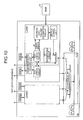
- Fig. 8 is a block diagram of the system board and the memory controller according to the third embodiment.
- the configuration of the SB and the memory controller according to the third embodiment is fundamentally the same as the configuration of the SB and the memory controller according to the second embodiment except the following description.
- the address-line-failure estimating circuit includes a counter, Decoder, OPSR, and a returning counter.
- the OPSR receives setting from the MMB 10, estimates that an error does not occur on an address line, and designates a counter value to make the switch control unit switch error data to a part of original request data for return.
- the ECC check circuit When the address-line-failure estimating circuit estimates that an error occurs on an address line, the ECC check circuit performs error rechecking through ECC, counts the number of times of no error, and outputs it to the Decoder.
- the address-line-failure estimating circuit determines whether the counter value output from the Decoder exceeds the upper-limit number of times designated from the OPSR. As a result of the determination, when the counter value exceeds the upper-limit number of times, the address-line-failure estimating circuit outputs a signal, to the switch control unit, to switch error data to a part of original request data for return.
- the upper-limit number of times can be altered by receiving change of setting from the MMB 10.
- the switch control unit When the switch control unit receives a signal from the address-line-failure estimating circuit, the switch control unit controls to switch error data to request data for return. More specifically, the switch control unit outputs a signal to the UE generating circuit to switch error data to a part of original request data.
- the determination result, by the address-line-failure estimating circuit, of whether the number of times when no error occurs exceeds the upper-limit number of times is not limited to when it is controlled that error data is switched to a part of original request data, for example, when the number of times when no errors continuously occur is counted and the number of times when no errors continuously occur exceeds the upper-limit number of times, the address-line-failure estimating circuit estimates that an error does not occur on an address line and can makes the switch control unit control to switch error data to a part of original request data.
- Fig. 9 is a flowchart for explaining processing of the memory controller according to the third embodiment. Processing after the address line failure circuit estimates that an error occurs on an address line and request data is switched to error data is explained in the following.
- step S901 when the address-line-failure estimating circuit estimates that an error occurs on an address line (yes at step S901), error checking is performed again through ECC (step S902), the number of times of no errors is counted, and it is output to the Decoder.
- the address-line-failure estimating circuit determines whether the counter value output from the Decoder exceeds the upper-limit number of times designated from the OPSR (step S903). As a result of the determination, when the counter value exceeds the upper-limit number of times (yes at step S903), the address-line-failure estimating circuit outputs a signal to the switch control unit to switch error data to a part of original request data for return. On the other hand, the address-line-failure estimating circuit does not particularly output a signal to the switch control unit when the counter value does not exceed the upper-limit number of times (no at step S903).
- the switch control unit when a signal is input from the address-line-failure estimating circuit, controls to switch error data to request data for return (step S905). More specifically, the switch control unit outputs a signal to the UE generating circuit to switch error data to a part of original request data.
- the third embodiment when it is estimated that an error occurs on an address line, error checking is performed again and it is determined that an error does not occur on an address line based on the resulting error checking that is performed again.
- generated error data is switched to data associated with request and control is performed to resume using data of one line of redundant memory. Accordingly, estimation of an error on an address line allows prevention of a system down as well as, for example, in consideration of a possibility of causing a temporary error due to not an error on an address line but a failure of a part of a cell in the DIMM, improvement of a cell' failure, if any, enables possible avoidance of lowering reliability because of single DIMM.
- the number of times of no errors obtained as the result of error checking that is performed again is counted and, when the number of times exceeds the predetermined upper-limit number of times, it is determined that an error does not occur on an address line.
- the predetermined upper-limit number of times to determine that an error does not occur on an address line is altered.
- a system maintainer arbitrarily sets the upper-limit number of times so that it is possible to avoid reliability t lowering because of single DIMM to the utmost.
- one DIMM connected to the LDX is explained, however, the present invention is not limited to the case of a single DIMM, and a plurality of DIMMs can be connected to the LDX.
- the LDX#01 has the DIMM1 and the DIMM0 arranged with the ECC check circuit respectively that constitutes an error checking unit.
- a system configuration of controlling two DIMMs through one memory controller allows estimation of an error on an address line, thereby enabling prevention of a system down.
- each ECC checking circuit exchanges its own ECC information (information for ECC checking) to perform ECC checking.
- a system configuration of controlling four DIMMs through one memory controller allows estimation of an error on an address line while controlling single DIMM to the minimum, thereby enabling prevention of a system down.
- each component of the memory controller (LDX#0) shown in Fig. 3 has a conceptual function and does not always physically have a configuration as illustrated in the drawing. That is, specific aspects of distributing and integrating the memory controller are not limited to its illustration.
- the ECC check circuit and the address-line-failure estimating circuit are integrated. Based on various loads or a using condition, the whole or a part of it can be functionally or physically distributed/integrated in an arbitrary unit for configuration.
- Each processing capability (address line failure estimating processing capability, data switching processing capability, and memory data returning determination processing capability) that is performed in the memory controller (LDX) described in the above embodiments can be realized by the MMB 10 reading and implementing a program stored in predetermined memory prepared in advance.
- a resulting error checking of data associated with a request when there is a request in a system for example, an error condition of data or a condition of the number of times when an error occurs
- an address line a line that transmits a data address of a request
- error data is created with respect to data of the request to switch the data to error data, thereby controlling not to use data of one line of redundant memory.
- a system configuration of controlling two DIMMs through one memory controller allows estimation of an error on an address line, thereby enabling prevention of a system down.
- a system configuration of controlling one DIMM through one memory controller has a higher capability than a system configuration of controlling two DIMMs through one memory controller, for example, thereby enabling prevention of a system down through estimation of an error on an address line.
- a system configuration of controlling four DIMMs through one memory controller allows estimation of an error on an address line while controlling single DIMM to the minimum, thereby enabling prevention of a system down.
- the predetermined upper-limit number of times to estimate that an error occurs on an address line is altered.
- a system maintainer arbitrarily sets the upper-limit number of times so that it is possible to prevent a system down.
- estimation of an error on an address line allows prevention of a system down as well as, for example, in consideration of a possibility of causing a temporary error due to not an error on an address line but a failure of a part of a cell in a DIMM, improvement of a cell' failure, if any, enables possible avoidance of reliability lowering because of a single DIMM.
- the predetermined upper-limit number of times to determine that an error does not occur on an address line is altered.
- a system maintainer arbitrarily sets the upper-limit number of times so that it is possible to avoid reliability lowering to the utmost because of a single DIMM.
Landscapes
- Engineering & Computer Science (AREA)
- Theoretical Computer Science (AREA)
- Physics & Mathematics (AREA)
- General Engineering & Computer Science (AREA)
- General Physics & Mathematics (AREA)
- Quality & Reliability (AREA)
- Techniques For Improving Reliability Of Storages (AREA)
- Hardware Redundancy (AREA)
- Debugging And Monitoring (AREA)
Claims (20)
- Speichercontroller (LDX#0-#3), der einen Speicher (DIMM-3) in einem System steuert, in dem eine Fehlerprüfeinheit zum Prüfen von Daten aus einer Vielzahl von Speichern (DIMM0-3) gebildet ist, von denen jeder ein Dualspeicher mit einer unabhängigen Adressleitung ist, welcher Speichercontroller (LDX#0-#3) gekennzeichnet ist durch:eine Fehlerschätzeinheit die dann, wenn eine Forderung nach Daten in dem System vorliegt, schätzt, ob ein Fehler auf der Adressleitung des Dualspeichers aufgetreten ist, auf der Basis eines Resultates eines Fehlerprüfprozesses zum Prüfen von Daten bezüglich der Forderung;eine Steuereinheit, die betriebsfähig ist, wenn durch die Fchlorschätzeinheit geschätzt wird, dass ein Fehler aufgetreten ist, um Fehlerdaten der Daten bezüglich der Forderung zu erzeugen und die Daten bezüglich der Forderung auf die erzeugten Fehlerdaten umzuschalten; undeine Vergleichseinheit (FLN), die den Speicher in solch einer Weise steuert, dass die genannte Leitung des Dualspeichers gesperrt wird, indem die erzeugten Fehlerdaten nicht für den angestrebten Vergleich eingesetzt werden.
- Speichercontroller (LDX#0-#3) nach Anspruch 1, bei dem die Fehlerschätzeinheit schätzt, ob ein Fehler auf der Adressleitung aufgetreten ist, auf der Basis eines Resultates einer Fehlerprüfung, die für eine Vielzahl von verbundenen Speichern (DIMM-3) ausgeführt wird.
- Speichercontroller (LDX#0-#3) nach Anspruch 1, bei dem die Fehlerschätzcinheit schätzt ob ein Fehler auf der Adressleitung aufgetreten ist, auf der Basis eines Resultates einer Fehlerprüfung, die für einen verbundenen Speicher ausgeführt wird.
- Speichercontroller (LDX#0-#3) nach Anspruch 1, bei dem die Fehlerschatzeinheit schätzt, ob ein Fehler auf der Adressleitung aufgetreten ist, auf der Basis eines Resultates einer Fehlerprüfung, die für jeden von einer Vielzahl von verbundenen Speichern (DIMM0-3) ausgeführt wird.
- Speichercontroller (LDX#0-#3) nach Anspruch 1, bei dem die Fehlerschätzeinheit die Anzahl des Male des Auftretens von unkorrigierbaren Fehlern zählt, die als Resultat der Fehlerprüfung erhalten werden, und schätzt, dass ein Fehler auf der Adressleitung ausgetreten ist, wenn die Anzahl der Male des Auftretens der unkorrigierbaren Fehler eine vorbestimmte Schwelle überschreitet.
- Speichercontroller (LDX#0-#3) nach Anspruch 5, ferner mit einer Veränderungseinheit (CPSR), welche die vorbestimmte Schwelle verändert.
- Speichercontroller (LDX#0-#3) nach Anspruch 1, ferner mit einer Bestimmungseinheit, die dann, wenn jeschätzt wird, dass ein Fehler auf der Adressleitung aufgetreten ist, die Fehlerprüfung wieder ausführt und auf der Basis eines Resultates der wiederausgeführten Fehlerprüfung bestimmt, ob ein Fehler auf der Adressleitung aufgetreten ist, bei dem
die Steuereinheit dann, wenn bestimmt wird, dass kein Fehler auf der Adressleitung aufgetreten ist, die erzeugten Fehlerdaten auf die Daten bezüglich der Forderung umschaltet und die Vergleichseinheit (FLN) den Speicher in solch einer Weise steuert, dass die eine Leistung des Dualspeichers freigegeben wird. - Speichercontroller (LDX#0-#3) nach Anspruch 7, bei dem die Bestimmungseinheit die Anzahl der Male des Nichtauftretens von Fehlern zählt, die als Resultat der wiederausgeführten Fehlerprüfung erhalten werden, und bestimmt, dass kein Fehler auf der Adressleitung aufgetreten ist, wenn die Anzahl der Male des Nichtauftretens von Fehlern eine vorbestimmte Schwelle überschreitet.
- Speichercontroller (LDX#0(7-#3) nach Anspruch 8, ferner mit einer Veränderungseinheit (OPSR), welche die vorbestimmte Schwelle verändert.
- verfahren zum Steuern eines Speichers in einem System, in dem eine Fehlerprüfeinheit für Daten aus einer Vielzahl von Speichern (DIMM0-3) gebildet ist, von denen jeder ein Dualspeicher mit einer unabhängigen Adressleitung ist, welches Verfahren gekennzeichnet ist durch:Schätzen (S403), wenn eine Forderung nach Daten in dem System vorliegt, ob ein Fehler auf der Adressleitung des Dualspeichers aufgetreten ist, auf der Basis eines Resultates eines Fehlerprüfprozesses (S402) für Daten bezüglich der Forderung;Erzeugen, wenn geschätzt wird, dass ein Fehler aufgetreten ist, von Fehlerdaten der Daten bezüglich der Forderung;Umschalten der Daten bezüglich der Forderung auf die erzeugten Fehlerdaten; undSteuern des Speichers in solch einer Weise, dass die genannte Leitung des Dualspeichers gesperrt wird, indem die erzeugten Fehlerdaten nicht für den angestrebten Vergleich eingesetzt werden (S405).
- Verfahren nach Anspruch 10, bei dem das Schätzen das Schätzen dessen enthält (S403), ob ein Fehler auf der Adressleitung aufgetreten ist, auf der Basis eines Resultates einer Fehlerprüfung, die für eine Vielzahl von verbundenen Speichern ausgeführt wird.
- Verfahren nach Anspruch 10, bei dem das Schätzen (S403) das Schätzen dessen enthält, ob ein Fehler auf der Adressleitung aufgetreten ist, auf der Basis eines Resultates einer Fehlerprüfung, die für einen verbundenen Speicher ausgeführt wirt.
- Verfahren nach Anspruch 10, bei dem das Schätzen (S403) das Schätzen dessen enthält, ob ein Fehler auf der Adressleitung aufgetreten ist, auf der Basis eines Resultattes einer Fehlerprüfung, die für jeden von einer Vielzahl von verbundenen Speichern ausgeführt wirt.
- Verfahren nach Anspruch 10, bei dem das Schützen (S703) enthält:Zähler der Anzahl der Male des Auftretens von unkorrigierbaren Fehler, die als Resultat der Fehlerprüfung erhalten werden, undSchätzen, dass ein Fehler auf der Adressleitung aufgetreten ist, wenn die Anzahl der Male des Auftretens der unkorrigierbaren Fehler eine vorbestimmte Schwelle überschreitet.
- Verfahren nach Anspruch 14, ferner mit dem Verändern der vorbestimmten Schwelle.
- Verfahren nach Anspruch 10, ferner mit dem Bestimmen, das enthält:Wiederausführen der Fehlerprüfung (S902), wenn geschätzt wird, dass ein Fehler auf der Adressleitung aufgetreten ist, undBestimmen, ob ein Fehler auf der Adressleitung aufgetreten ist, auf der Basis eines Resultates der wiederausgeführten Fehlerprüfung, bei demdas Umschalten enthält :Umschalten (S904), wenn bestimmt wird, dass kein Fehler auf der Adressleitung aufgetreten ist, der erzeugten Fehlerdaten auf die Daten bezüglich der Forderung, unddas Steuern enthält:Steuern des Speichers in solch einer Weise, dass die genannte Leitung des Dualspeichers freigegeben wird.
- Verfahren nach Anspruch 16, bei dem das Bestimmen enthält,:Zählen der Anzahl der Male des Nichtauftretens von Fehlern, die als Resultat der wiederausgeführten Fehlerprüfung erhalten werden, undBestimmen, dass kein Fehler auf der Adressleitung aufgetreten ist, wenn die Anzahl der Male des Nichtauftretens von Fehlern eine vorbestimmte Schwelle überschreitet (S903).
- Verfahren nach Anspruch 17, ferner mit dem Verändern der vorbestimmten Schwelle.
- Computerlesbares Aufzeichnungsmedium, das ein Computerprograrnm zum Steuern eines Speichers (DIMM0-3) in einem System speichert, in dem eine Fehlerprüfeinheit zum Prüfen von Daten aus einer Vielzahl von Speichern (DIMM0-3) gebildet ist, von denen jeder ein Dualspeicher mit einer unabhängigen Adressleitung ist, welches computerprogramm dadurch gekennzeichnet ist, dass es bewirkt, dass ein Computer ausführt:Schätzen (S403), wenn eine Forderung nach Daten in dem System vorliegt, ob ein Fehler auf der Adressleitung des Dualspeichers aufgetreten ist, auf der Basis eines Resultattes eines Fehlerprüfprozesses (S402) für Daten bezüglich der Forderung;Erzeugen, wenn geschätzt wird, dass ein Fehler aufgetreten ist, von Fehlerdaten der Daten bezüglich der Forderung;Umschalten (S404) der Daten bezüglich der Forderung auf die erzeugten Fehlerdaten; undSteuern des Speichers in solch einer weise, dass die genannte Leitung des Dualspeichers gesperrt wird, indem die erzeugten Fehlerdaten nicht für den angestrebten Vergleich eingesetzt werden (S405).
- Computerlesbares Aufzeichnungsmedium nach Anspruch 19, bei dem das Schätzen (S403) das Schützen dessen enthält, ob ein Fehler auf der Adressleitung aufgetreten ist, auf der Basis eines Resultates einer Fehlerprüfung, die für einen verbundenen Speicher ausgeführt wird.
Applications Claiming Priority (1)
| Application Number | Priority Date | Filing Date | Title |
|---|---|---|---|
| JP2006223489A JP4918824B2 (ja) | 2006-08-18 | 2006-08-18 | メモリコントローラおよびメモリ制御方法 |
Publications (2)
| Publication Number | Publication Date |
|---|---|
| EP1890239A1 EP1890239A1 (de) | 2008-02-20 |
| EP1890239B1 true EP1890239B1 (de) | 2010-12-29 |
Family
ID=38324123
Family Applications (1)
| Application Number | Title | Priority Date | Filing Date |
|---|---|---|---|
| EP07106725A Ceased EP1890239B1 (de) | 2006-08-18 | 2007-04-23 | Speichersteuerung und Verfahren zur Speichersteuerung |
Country Status (6)
| Country | Link |
|---|---|
| US (1) | US8667372B2 (de) |
| EP (1) | EP1890239B1 (de) |
| JP (1) | JP4918824B2 (de) |
| KR (1) | KR100878550B1 (de) |
| CN (1) | CN101127243B (de) |
| DE (1) | DE602007011535D1 (de) |
Families Citing this family (17)
| Publication number | Priority date | Publication date | Assignee | Title |
|---|---|---|---|---|
| US7562285B2 (en) | 2006-01-11 | 2009-07-14 | Rambus Inc. | Unidirectional error code transfer for a bidirectional data link |
| US8352805B2 (en) * | 2006-05-18 | 2013-01-08 | Rambus Inc. | Memory error detection |
| JP4962381B2 (ja) * | 2008-03-28 | 2012-06-27 | 富士通株式会社 | 情報処理装置、情報処理装置制御方法および情報処理装置制御プログラム |
| JP5293062B2 (ja) * | 2008-10-03 | 2013-09-18 | 富士通株式会社 | コンピュータ装置、メモリ診断方法、及びメモリ診断制御プログラム |
| JP5267166B2 (ja) * | 2009-01-30 | 2013-08-21 | ソニー株式会社 | インターフェース装置、演算処理装置、インターフェース生成装置、および回路生成装置 |
| EP2482194B1 (de) | 2009-09-25 | 2013-12-25 | Fujitsu Limited | Speichersystem und steuerverfahren für ein speichersystem |
| US9613715B2 (en) | 2014-06-16 | 2017-04-04 | Sandisk Technologies Llc | Low-test memory stack for non-volatile storage |
| US9606882B2 (en) * | 2014-07-17 | 2017-03-28 | Sandisk Technologies Llc | Methods and systems for die failure testing |
| US10002043B2 (en) * | 2014-08-19 | 2018-06-19 | Samsung Electronics Co., Ltd. | Memory devices and modules |
| KR102214556B1 (ko) * | 2014-08-19 | 2021-02-09 | 삼성전자주식회사 | 메모리 장치 및 모듈 |
| US20160055058A1 (en) * | 2014-08-19 | 2016-02-25 | Hongzhong Zheng | Memory system architecture |
| US10002044B2 (en) * | 2014-08-19 | 2018-06-19 | Samsung Electronics Co., Ltd. | Memory devices and modules |
| US9594623B2 (en) * | 2015-03-24 | 2017-03-14 | Nxp Usa, Inc. | System on chip and method of updating program code on a system on chip |
| US9916091B2 (en) | 2015-07-13 | 2018-03-13 | Samsung Electronics Co., Ltd. | Memory system architecture |
| US9892024B2 (en) * | 2015-11-02 | 2018-02-13 | Sony Interactive Entertainment America Llc | Backward compatibility testing of software in a mode that disrupts timing |
| DE102016223341A1 (de) * | 2016-11-24 | 2018-05-24 | Robert Bosch Gmbh | Integrierte Schaltung mit Hardwareprüfeinheit zum Überprüfen von ausgewählten Speicherzugriffen |
| CN111819547B (zh) | 2018-03-26 | 2025-02-07 | 拉姆伯斯公司 | 命令/地址通道错误检测 |
Family Cites Families (34)
| Publication number | Priority date | Publication date | Assignee | Title |
|---|---|---|---|---|
| JPS55157043A (en) | 1979-05-28 | 1980-12-06 | Toshiba Corp | Information processor |
| JPS6035695B2 (ja) * | 1980-08-06 | 1985-08-16 | 富士通株式会社 | メモリ試験方式 |
| JPS57150197A (en) * | 1981-03-11 | 1982-09-16 | Nippon Telegr & Teleph Corp <Ntt> | Storage circuit |
| JPS58127242A (ja) | 1982-01-25 | 1983-07-29 | Nec Corp | 論理回路 |
| JPS592294A (ja) * | 1982-06-01 | 1984-01-07 | Fujitsu Ltd | メモリ装置の試験方式 |
| JPH0620200B2 (ja) * | 1982-10-08 | 1994-03-16 | 株式会社日立製作所 | データ通信方式 |
| JPS608962A (ja) | 1983-06-29 | 1985-01-17 | Fujitsu Ltd | 記憶情報一時障害検出方式 |
| NL8400392A (nl) * | 1984-02-08 | 1985-09-02 | Philips Nv | Inrichting voor de functiebewaking van een geheugeninrichting. |
| US4774712A (en) * | 1986-10-01 | 1988-09-27 | International Business Machines Corporation | Redundant storage device having address determined by parity of lower address bits |
| GB8815239D0 (en) * | 1988-06-27 | 1988-08-03 | Wisdom Systems Ltd | Memory error protection system |
| US5058115A (en) * | 1989-03-10 | 1991-10-15 | International Business Machines Corp. | Fault tolerant computer memory systems and components employing dual level error correction and detection with lock-up feature |
| JPH02238539A (ja) * | 1989-03-13 | 1990-09-20 | Hitachi Ltd | メモリ制御方式 |
| US5164944A (en) * | 1990-06-08 | 1992-11-17 | Unisys Corporation | Method and apparatus for effecting multiple error correction in a computer memory |
| JPH05225089A (ja) * | 1992-02-07 | 1993-09-03 | Nec Eng Ltd | データ転送装置 |
| SE470544B (sv) * | 1992-11-24 | 1994-07-25 | Ellemtel Utvecklings Ab | För en bitfelsövervakning i en väljarutrustning avsedd anordning |
| JPH07160587A (ja) * | 1993-12-07 | 1995-06-23 | Fujitsu Ltd | 多重化メモリ装置 |
| JP3436974B2 (ja) * | 1994-06-27 | 2003-08-18 | 三菱電機株式会社 | 二重化メモリシステム |
| US5768294A (en) * | 1995-12-11 | 1998-06-16 | International Business Machines Corporation | Memory implemented error detection and correction code capable of detecting errors in fetching data from a wrong address |
| JPH09288619A (ja) * | 1996-04-22 | 1997-11-04 | Mitsubishi Electric Corp | 主記憶装置 |
| US6408195B1 (en) * | 1996-07-04 | 2002-06-18 | Seiko Instruments Inc. | Semiconductor integrated circuit for communication and battery saving method for the same |
| US5905858A (en) * | 1996-11-01 | 1999-05-18 | Micron Electronics, Inc. | System for method memory error handling |
| US5978953A (en) * | 1996-12-19 | 1999-11-02 | Compaq Computer Corporation | error detection and correction |
| JP3199021B2 (ja) * | 1998-03-19 | 2001-08-13 | 日本電気株式会社 | 半導体メモリ装置、該半導体メモリ装置の検査方法及び使用方法 |
| US6842867B2 (en) * | 2001-01-26 | 2005-01-11 | Dell Products L.P. | System and method for identifying memory modules having a failing or defective address |
| US6792567B2 (en) | 2001-04-30 | 2004-09-14 | Stmicroelectronics, Inc. | System and method for correcting soft errors in random access memory devices |
| DE10255872B4 (de) * | 2002-11-29 | 2004-09-30 | Infineon Technologies Ag | Speichermodul und Verfahren zum Betrieb eines Speichermoduls in einem Datenspeichersystem |
| CN1532701B (zh) * | 2003-03-20 | 2010-04-28 | 纬创资通股份有限公司 | 存储器不稳定仍维持系统稳定度的系统及存储器控制方法 |
| US7234099B2 (en) * | 2003-04-14 | 2007-06-19 | International Business Machines Corporation | High reliability memory module with a fault tolerant address and command bus |
| JP2003337758A (ja) | 2003-05-01 | 2003-11-28 | Mitsubishi Electric Corp | 二重化メモリシステム |
| JP2005056200A (ja) * | 2003-08-05 | 2005-03-03 | Hitachi Ltd | データ管理方法、ディスク記憶装置およびディスク記憶システム |
| US7203890B1 (en) * | 2004-06-16 | 2007-04-10 | Azul Systems, Inc. | Address error detection by merging a polynomial-based CRC code of address bits with two nibbles of data or data ECC bits |
| US20060077750A1 (en) * | 2004-10-07 | 2006-04-13 | Dell Products L.P. | System and method for error detection in a redundant memory system |
| US7185246B2 (en) * | 2004-12-15 | 2007-02-27 | International Business Machines Corporation | Monitoring of solid state memory devices in active memory system utilizing redundant devices |
| KR100877701B1 (ko) * | 2006-11-23 | 2009-01-08 | 삼성전자주식회사 | 반도체 메모리 장치 및 이 장치의 리던던시 방법 |
-
2006
- 2006-08-18 JP JP2006223489A patent/JP4918824B2/ja not_active Expired - Fee Related
-
2007
- 2007-04-23 EP EP07106725A patent/EP1890239B1/de not_active Ceased
- 2007-04-23 DE DE602007011535T patent/DE602007011535D1/de active Active
- 2007-04-26 US US11/790,669 patent/US8667372B2/en not_active Expired - Fee Related
- 2007-05-18 KR KR1020070048555A patent/KR100878550B1/ko not_active Expired - Fee Related
- 2007-05-22 CN CN2007101050811A patent/CN101127243B/zh not_active Expired - Fee Related
Also Published As
| Publication number | Publication date |
|---|---|
| US20080046802A1 (en) | 2008-02-21 |
| CN101127243A (zh) | 2008-02-20 |
| KR100878550B1 (ko) | 2009-01-14 |
| KR20080016435A (ko) | 2008-02-21 |
| CN101127243B (zh) | 2012-05-02 |
| JP4918824B2 (ja) | 2012-04-18 |
| DE602007011535D1 (de) | 2011-02-10 |
| JP2008046979A (ja) | 2008-02-28 |
| EP1890239A1 (de) | 2008-02-20 |
| US8667372B2 (en) | 2014-03-04 |
Similar Documents
| Publication | Publication Date | Title |
|---|---|---|
| EP1890239A1 (de) | Speichersteuerung und Verfahren zur Speichersteuerung | |
| US6505305B1 (en) | Fail-over of multiple memory blocks in multiple memory modules in computer system | |
| US7984357B2 (en) | Implementing minimized latency and maximized reliability when data traverses multiple buses | |
| EP0514075A2 (de) | Fehlertoleranter Datenverarbeitungsteil mit dynamisch rekonfigurierbarer Mehrkeitsentscheidung | |
| US20040168101A1 (en) | Redundant memory system and memory controller used therefor | |
| JP2012113466A (ja) | メモリコントローラ及び情報処理システム | |
| US8140940B2 (en) | Method and apparatus for controlling memory | |
| KR102378466B1 (ko) | 메모리 장치 및 모듈 | |
| EP1703398B1 (de) | Techniken zur Korrektur von Software-Fehlern | |
| CN102915260B (zh) | 固态硬盘容错的方法及其固态硬盘 | |
| EP1116114B1 (de) | Detektionstechnik von speicherabschnittfehlern und einzel-, doppel und triplebitfehlern | |
| CN115168087A (zh) | 一种确定内存故障的修复资源粒度的方法及装置 | |
| KR101448013B1 (ko) | 항공기용 다중 컴퓨터의 고장 허용 장치 및 방법 | |
| US7246257B2 (en) | Computer system and memory control method thereof | |
| US5590278A (en) | Method for detecting addressing errors in an electrical unit | |
| US8176388B1 (en) | System and method for soft error scrubbing | |
| US8261137B2 (en) | Apparatus, a method and a program thereof | |
| JP2009187314A (ja) | 二重化コントローラ・システム、cpuモジュール、そのプログラム | |
| JPS6391764A (ja) | パリティ・チェック機能を有するメモリ・システム | |
| JP5910356B2 (ja) | 電子装置、電子装置制御方法及び電子装置制御プログラム | |
| EP3882774B1 (de) | Datenverarbeitungsvorrichtung | |
| JP5964265B2 (ja) | 半導体集積回路装置 | |
| US12499008B2 (en) | Control register related computing system and method | |
| EP4506806A1 (de) | Speichervorrichtung und datenverarbeitungsverfahren | |
| JP3311776B2 (ja) | ディスクサブシステムにおけるデータ転送チェック方式 |
Legal Events
| Date | Code | Title | Description |
|---|---|---|---|
| PUAI | Public reference made under article 153(3) epc to a published international application that has entered the european phase |
Free format text: ORIGINAL CODE: 0009012 |
|
| AK | Designated contracting states |
Kind code of ref document: A1 Designated state(s): AT BE BG CH CY CZ DE DK EE ES FI FR GB GR HU IE IS IT LI LT LU LV MC MT NL PL PT RO SE SI SK TR |
|
| AX | Request for extension of the european patent |
Extension state: AL BA HR MK YU |
|
| 17P | Request for examination filed |
Effective date: 20080328 |
|
| AKX | Designation fees paid |
Designated state(s): DE FR GB |
|
| GRAP | Despatch of communication of intention to grant a patent |
Free format text: ORIGINAL CODE: EPIDOSNIGR1 |
|
| GRAS | Grant fee paid |
Free format text: ORIGINAL CODE: EPIDOSNIGR3 |
|
| GRAA | (expected) grant |
Free format text: ORIGINAL CODE: 0009210 |
|
| AK | Designated contracting states |
Kind code of ref document: B1 Designated state(s): DE FR GB |
|
| REG | Reference to a national code |
Ref country code: GB Ref legal event code: FG4D |
|
| REF | Corresponds to: |
Ref document number: 602007011535 Country of ref document: DE Date of ref document: 20110210 Kind code of ref document: P |
|
| REG | Reference to a national code |
Ref country code: DE Ref legal event code: R096 Ref document number: 602007011535 Country of ref document: DE Effective date: 20110210 |
|
| PLBE | No opposition filed within time limit |
Free format text: ORIGINAL CODE: 0009261 |
|
| STAA | Information on the status of an ep patent application or granted ep patent |
Free format text: STATUS: NO OPPOSITION FILED WITHIN TIME LIMIT |
|
| 26N | No opposition filed |
Effective date: 20110930 |
|
| REG | Reference to a national code |
Ref country code: DE Ref legal event code: R097 Ref document number: 602007011535 Country of ref document: DE Effective date: 20110930 |
|
| REG | Reference to a national code |
Ref country code: FR Ref legal event code: PLFP Year of fee payment: 10 |
|
| REG | Reference to a national code |
Ref country code: FR Ref legal event code: PLFP Year of fee payment: 11 |
|
| REG | Reference to a national code |
Ref country code: FR Ref legal event code: PLFP Year of fee payment: 12 |
|
| PGFP | Annual fee paid to national office [announced via postgrant information from national office to epo] |
Ref country code: GB Payment date: 20240320 Year of fee payment: 18 |
|
| PGFP | Annual fee paid to national office [announced via postgrant information from national office to epo] |
Ref country code: FR Payment date: 20240320 Year of fee payment: 18 |
|
| PGFP | Annual fee paid to national office [announced via postgrant information from national office to epo] |
Ref country code: DE Payment date: 20240320 Year of fee payment: 18 |
|
| REG | Reference to a national code |
Ref country code: DE Ref legal event code: R119 Ref document number: 602007011535 Country of ref document: DE |
|
| GBPC | Gb: european patent ceased through non-payment of renewal fee |
Effective date: 20250423 |
|
| PG25 | Lapsed in a contracting state [announced via postgrant information from national office to epo] |
Ref country code: DE Free format text: LAPSE BECAUSE OF NON-PAYMENT OF DUE FEES Effective date: 20251104 |
|
| PG25 | Lapsed in a contracting state [announced via postgrant information from national office to epo] |
Ref country code: GB Free format text: LAPSE BECAUSE OF NON-PAYMENT OF DUE FEES Effective date: 20250423 |
|
| PG25 | Lapsed in a contracting state [announced via postgrant information from national office to epo] |
Ref country code: FR Free format text: LAPSE BECAUSE OF NON-PAYMENT OF DUE FEES Effective date: 20250430 |