EP1889528B1 - Heat transfer surface for electronic cooling - Google Patents
Heat transfer surface for electronic cooling Download PDFInfo
- Publication number
- EP1889528B1 EP1889528B1 EP06772321A EP06772321A EP1889528B1 EP 1889528 B1 EP1889528 B1 EP 1889528B1 EP 06772321 A EP06772321 A EP 06772321A EP 06772321 A EP06772321 A EP 06772321A EP 1889528 B1 EP1889528 B1 EP 1889528B1
- Authority
- EP
- European Patent Office
- Prior art keywords
- fins
- channels
- sets
- tips
- cooling surface
- Prior art date
- Legal status (The legal status is an assumption and is not a legal conclusion. Google has not performed a legal analysis and makes no representation as to the accuracy of the status listed.)
- Active
Links
Images


Classifications
-
- H—ELECTRICITY
- H05—ELECTRIC TECHNIQUES NOT OTHERWISE PROVIDED FOR
- H05K—PRINTED CIRCUITS; CASINGS OR CONSTRUCTIONAL DETAILS OF ELECTRIC APPARATUS; MANUFACTURE OF ASSEMBLAGES OF ELECTRICAL COMPONENTS
- H05K7/00—Constructional details common to different types of electric apparatus
- H05K7/20—Modifications to facilitate cooling, ventilating, or heating
-
- H—ELECTRICITY
- H01—ELECTRIC ELEMENTS
- H01L—SEMICONDUCTOR DEVICES NOT COVERED BY CLASS H10
- H01L23/00—Details of semiconductor or other solid state devices
- H01L23/34—Arrangements for cooling, heating, ventilating or temperature compensation ; Temperature sensing arrangements
- H01L23/42—Fillings or auxiliary members in containers or encapsulations selected or arranged to facilitate heating or cooling
- H01L23/427—Cooling by change of state, e.g. use of heat pipes
-
- B—PERFORMING OPERATIONS; TRANSPORTING
- B21—MECHANICAL METAL-WORKING WITHOUT ESSENTIALLY REMOVING MATERIAL; PUNCHING METAL
- B21J—FORGING; HAMMERING; PRESSING METAL; RIVETING; FORGE FURNACES
- B21J5/00—Methods for forging, hammering, or pressing; Special equipment or accessories therefor
- B21J5/06—Methods for forging, hammering, or pressing; Special equipment or accessories therefor for performing particular operations
- B21J5/068—Shaving, skiving or scarifying for forming lifted portions, e.g. slices or barbs, on the surface of the material
-
- F—MECHANICAL ENGINEERING; LIGHTING; HEATING; WEAPONS; BLASTING
- F28—HEAT EXCHANGE IN GENERAL
- F28F—DETAILS OF HEAT-EXCHANGE AND HEAT-TRANSFER APPARATUS, OF GENERAL APPLICATION
- F28F3/00—Plate-like or laminated elements; Assemblies of plate-like or laminated elements
- F28F3/02—Elements or assemblies thereof with means for increasing heat-transfer area, e.g. with fins, with recesses, with corrugations
- F28F3/04—Elements or assemblies thereof with means for increasing heat-transfer area, e.g. with fins, with recesses, with corrugations the means being integral with the element
- F28F3/048—Elements or assemblies thereof with means for increasing heat-transfer area, e.g. with fins, with recesses, with corrugations the means being integral with the element in the form of ribs integral with the element or local variations in thickness of the element, e.g. grooves, microchannels
-
- F—MECHANICAL ENGINEERING; LIGHTING; HEATING; WEAPONS; BLASTING
- F28—HEAT EXCHANGE IN GENERAL
- F28F—DETAILS OF HEAT-EXCHANGE AND HEAT-TRANSFER APPARATUS, OF GENERAL APPLICATION
- F28F3/00—Plate-like or laminated elements; Assemblies of plate-like or laminated elements
- F28F3/12—Elements constructed in the shape of a hollow panel, e.g. with channels
-
- H—ELECTRICITY
- H01—ELECTRIC ELEMENTS
- H01L—SEMICONDUCTOR DEVICES NOT COVERED BY CLASS H10
- H01L23/00—Details of semiconductor or other solid state devices
- H01L23/34—Arrangements for cooling, heating, ventilating or temperature compensation ; Temperature sensing arrangements
- H01L23/46—Arrangements for cooling, heating, ventilating or temperature compensation ; Temperature sensing arrangements involving the transfer of heat by flowing fluids
- H01L23/473—Arrangements for cooling, heating, ventilating or temperature compensation ; Temperature sensing arrangements involving the transfer of heat by flowing fluids by flowing liquids
-
- H—ELECTRICITY
- H01—ELECTRIC ELEMENTS
- H01L—SEMICONDUCTOR DEVICES NOT COVERED BY CLASS H10
- H01L2924/00—Indexing scheme for arrangements or methods for connecting or disconnecting semiconductor or solid-state bodies as covered by H01L24/00
- H01L2924/0001—Technical content checked by a classifier
- H01L2924/0002—Not covered by any one of groups H01L24/00, H01L24/00 and H01L2224/00
-
- Y—GENERAL TAGGING OF NEW TECHNOLOGICAL DEVELOPMENTS; GENERAL TAGGING OF CROSS-SECTIONAL TECHNOLOGIES SPANNING OVER SEVERAL SECTIONS OF THE IPC; TECHNICAL SUBJECTS COVERED BY FORMER USPC CROSS-REFERENCE ART COLLECTIONS [XRACs] AND DIGESTS
- Y10—TECHNICAL SUBJECTS COVERED BY FORMER USPC
- Y10T—TECHNICAL SUBJECTS COVERED BY FORMER US CLASSIFICATION
- Y10T29/00—Metal working
- Y10T29/49—Method of mechanical manufacture
- Y10T29/4935—Heat exchanger or boiler making
Definitions
- the invention generally relates to a cooling surface that can be conductively attached to and cool electronic components.
- Electronic devices such as computers, process information on computer chips and these chips generate heat during use. The faster or longer the chips process information the hotter they become. If the chips become too hot they will bum up or otherwise malfunction.
- structures are provided in electronics to cool the chips during processing. For example, computers have fans that activate if the computer detects that the chips are getting too hot.
- a computer may be arranged to slow processing if it detects the chips are getting too hot.
- conductive structures are attached adjacent to the chip to conduct heat away from the chip to those structures.
- Such structures can take a variety of forms. For example, copper blocks have been attached to chips so that the heat conducts from the chip to its attached block. Fins have been provided on a single surface of such blocks to enhance heat transfer. Oftentimes these structures cannot cool the chips sufficiently, however, so ultimately the chips bum up or otherwise malfunction.
- US4369838 discloses a cooling surface (“heat releasing device") having the features of the preamble of claim 1.
- This invention provides a cooling surface for electronic components, such as electronic chips, that better facilitates electronic cooling. While for ease of discussion the cooling surface is described for use with an electronic chip, applicants in no way intend that the surface be used only with electronic chips. Rather, one of skill in the art will recognize that the surface may be used with any electronic component for which facilitation of cooling is desirable.
- a first set of fins that define a first set of channels is provided on one side of the surface. The first set of fins and channels are oriented on the surface at a first orientation.
- a second set of fins that define a second set of channels is provided on the side of the surface opposite the first set of fins and channels. The second set of fins and channels are oriented on the surface at a second orientation, preferably at an angle relative to the first orientation. Passageways connecting the first and second set of channels extend through the surface.
- the cooling surface is attached to an electronic chip.
- the tips of the first set of fins can be flattened to facilitate attachment of the cooling surface (via the first fins) to the electronic chip.
- Liquid refrigerant is supplied to at least one of the sets of channels, preferably the first set of channels proximate to the electronic chip. As liquid is supplied to the cooling surface, the first set of channels fills with liquid refrigerant. The liquid refrigerant flows through the passageways and into the second set of channels. In so doing, the liquid refrigerant coats the walls of the sets of fins.
- the cooling surface conducts heat away from the chip.
- the heat is then transferred to the refrigerant that is coated on the fins of the cooling surface.
- At least some of the refrigerant vaporizes, and the resulting vapors escape through the passageways in the surface and away from the chip.
- an electronics cooling surface There is provided an electronics cooling surface, a method of forming an electronics cooling surface, and an electronics cooling system.
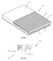
- FIG. 1 is a perspective view of a cooling surface according to one embodiment of the invention.
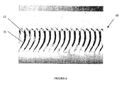
- FIG. 2 is a partial end view of the cooling surface of FIG. 1 illustrating the lower fins.
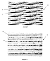
- FIG. 3 is a photomicrograph of a cross-sectional view of the lower fins of a cooling surface according to an embodiment of the invention.
- FIG. 4 is a photomicrograph of a cross-sectional view of the upper fins of a cooling surface according to an embodiment of the invention.
- FIG. 5 is a photomicrograph of a cross-sectional view of the upper fins of a cooling surface according to another embodiment of the invention.
- FIG. 6 is a photomicrograph of a cross-sectional view of the lower fins of a cooling surface according to another embodiment of the invention.
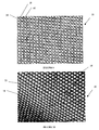
- FIG. 7 is a photomicrograph of a top plan view of a cooling surface according to still another embodiment of the invention.
- FIG. 8 is a photomicrograph of a bottom plan view of a cooling surface according to still another embodiment of the invention.
- FIG. 9 is a photomacrograph of a top plan view of an electronics cooling surface in accordance with an embodiment of the invention.
- FIG. 10 is a photomacrograph of a top plan view of an electronics cooling surface in accordance with an embodiment of the invention, shown after stretching.
- Figure 1 illustrates one embodiment of a partially-formed surface 10 of this invention.
- the surface 10 includes two sets of channels 12, 14 formed by two sets of fins 16, 18, respectively.
- the surface 10 is preferably, but does not have to be, attached to a microchip (not shown) so that the lower set of channels 12 is positioned adjacent to the chip and runs in a first direction and the upper set of channels 14 is positioned above the lower set of channels 12 and runs in a second direction that is at an angle to the first direction.
- the sets of channels 12, 14 are interconnected to one another by a plurality of passageways 20 (see Figure 9 ).
- the surface 10 is preferably formed from a blank of conductive material, such as metal (including copper, titanium, aluminum, gold, stainless steel, etc.) and more preferably copper.
- the surface 10 can be formed of any highly-conductive material, however, such as a carbide with a high carbon content. Carbon itself could be used to form the surface 10.
- Figure 1 illustrates a partially-formed surface 10 formed from a blank 11.
- fins 16, 18 are preferably, but do not have to be, formed over the entirety of the blank 11.
- a lower set of upstanding fins 16 is formed on one side of the blank 11, thereby creating the lower set of channels 12 between the adjacent fins 16.
- An upper set of upstanding fins 18 is then formed on the opposite side of the blank 11, thereby creating the upper set of channels 14 between the adjacent fins 18.
- the sets of fins 16, 18 may be formed by many methods known in the art, but preferably are formed by cutting the sets of fins 16, 18 and subsequently lifting the sets of fins 16, 18 to a desirable angle.
- the sets of fins 16, 18 are formed by cutting layers in the surface of the blank 11 and lifting the cut layers to a desirable angle to form upstanding sets of fins 16, 18.
- This cutting and lifting method and a tool for performing this method are disclosed in copending applications US 2004-0069467 and US 2005-0145377 .
- the sets of fins 16, 18 may be formed on a flat blank, in a preferable method, the uncut blank is wrapped around a rotatable drum so that the surface of the blank is curved in a semicircle. In this configuration, the blank emulates a tube surface and conventional tube surface enhancement techniques may be used on each side of the blank to form fins 16, 18. It makes no difference which set of fins 16, 18 (and thus which set of channels 12, 14) are formed in the blank first.
- channels 12, 14 formed by fins 16, 18 extend slightly beyond the centerline of the thickness of the blank 11.
- passageways 20 are formed at the intersection of and extend between the upper and lower set of channels 12, 14.
- the portion of channel 12 that extends beyond the centerline of the blank intersects with the corresponding portion of channel 14 that extends beyond the centerline.
- This intersection forms a passageway 20 between the two channels 12, 14.
- Figures 9 and 10 illustrate the passageways 20. While it is preferable that the channels of both sets of channels 12, 14 extend beyond the centerline of the blank thickness, the channels of only one set of channels 12, 14 may so extend to form the passageways 20.
- fin pitch is defined as the width of a single channel plus the thickness of one of the fins defining the channel.
- the fin pitch of the upper and lower sets of fins 16, 18 is preferably, but does not have to be, between 20-1200 fins per inch (0.79 - 47 fins per mm).
- the fin pitch may vary between the lower and upper sets of fins 16, 18 so that the lower set of fins 16 has a different fin pitch than the upper set of fins 18.
- the fin pitch can vary within each set of fins 16, 18, so that for example a portion of the upper set of fins 18 has a different fin pitch than another portion of the upper set of fins 18.
- the height of the fins 16, 18 may also vary between the sets of fins 16, 18 so that the lower set of fins 16 has a different fin height than the upper set of fins 18.
- the fin height can vary within each set of fins 16, 18, so that for example a portion of the upper set of fins 18 has a different fin height than another portion of the upper set of fins 18.
- the optimal geometries of the sets of fins 16, 18 and the sets of channels 12, 14 will depend on a number of factors, including the type of refrigerant used and the amount of heat needed to be conducted away from the surface 10. It is preferable, but not necessary, that the aspect ratio A for each set of fins 16, 18 (defined as the fin height divided by the channel width) be in the range between 0.1 ⁇ A ⁇ 400 and more preferably between 0.1 ⁇ A ⁇ 40.
- Figure 3 is a cross-sectional view showing the lower set of channels 12 of surface 10 formed by fins 16 having a fin pitch of 100 fins/inch (3.9 fins/mm) and a fin height of .023 inches (0.58 mm).
- Figure 4 is a cross-sectional view showing the upper set of channels 14 of surface 10 formed by fins 18 having a fin pitch of 200 fins/inch (7.9 fins/mm) and a fin height of approximately .0205 inches (0.521 mm).
- Figure 5 is a cross-sectional view showing the upper set of channels 14 of surface 10 formed by fins 18 having a fin pitch of 200 fins/inch (7.9 fins/mm) and a fin height of approximately .0175 inches (0.445 mm).
- Figure 6 is a cross-sectional view showing the lower set of channels 12 of surface 10 formed by fins 16 having a fin pitch of 200 fins/inch (7.9 fins/mm) and a fin height of approximately .021 inches (0.53 mm).
- Figure 7 is a plan view of the upper set of fins 18 forming channels 14.
- surface 10 is preferably attached to a chip so that the lower set of channels 12 is proximal to the chip.
- the surface 10 can be attached to the chip in any number of ways, including by soldering or using an adhesive or paste. It is preferable that the adhesive or paste used be conductive to further facilitate cooling of the chips.
- the tips of the lower set of fins 16 be flattened, as shown in Figures 2 , 3 , and 6 . Such flattening creates additional surface area for attachment to the chip. Moreover, the additional surface area provided by flattened tips of the lower set of fins 16 assists in the conduction of heat.
- Figure 8 is a plan view of the lower set of fins 16 forming channels 12. The fins of the lower set of fins 16 have been flattened.
- the tips of the set of fins 16 may be flattened using conventional flattening techniques or those described in US 2005-0145377 .
- the tips of the set of fins 16 may also be bent over to form a relatively flat surface or cut so as to have thickened tips and thus create more surface area at the tips for attachment.
- Methods and tools for bending and thickening fin tips, as well as angling adjacent fin tips relative to each other are also described in US 2005-0145377 . It is within the scope of the present invention to flatten or otherwise enhance the tips of the upper set of fins 18 in addition to or instead of flattening the tips of the lower set of fins 16.
- a liquid refrigerant is supplied to at least one of the sets of channels 12, 14. It is preferred that refrigerant is supplied at least to the lower set of channels 12. Any number of refrigerants can be used, including but not limited to water or HFE-7100, which is manufactured by 3M. Alternatively, manufacturers such as DuPont or Allied Signal manufacture refrigerants known as 134A or 123 that are also appropriate for use in the current invention.
- the refrigerant runs through the lower set of channels 12 to coat the surface of the lower set of fins 16. As the lower set of channels 12 becomes filled with the refrigerant, the refrigerant is discharged through the passageways 20, and into the upper set of channels 14 to coat at least some of the surface of the upper set of fins 18.
- refrigerant may be supplied directly to the upper set of channels 14 instead of or in addition to supplying refrigerant to the lower set of channels 12.
- the heat generated by the chip is transferred to the conductive surface 10.
- the temperature of the liquid refrigerant in channels 12, 14 elevates, converting at least some of the liquid refrigerant to vapor.
- At least some of the vapor produced in the lower set of channels 12 is discharged through passageways 20 and into the upper set of channels 14, thereby carrying heat away from the chip.
- heat generated by the chip is carried away in that refrigerant. In this way, heat generated by the chip is carried away by the refrigerant, either in liquid or vapor form.
- a pump (not shown) can be used to pump the liquid refrigerant into one or both of the channels 12, 14 and thereby prevent all of the refrigerant from vaporizing. Rather, while some of the refrigerant will turn to vapor during the heat transfer process, the pump replenishes the refrigerant to the cooling surface 10 so that a combination of liquid refrigerant and vapor is present in the sets of channels 12, 14.
- the pump can continuously supply refrigerant to the sets of channels 12, 14.
- a controller for the pump may be used to monitor the temperature of the chip and activate the pump only when the temperature increases to a predetermined amount.
- Supplying refrigerant to the sets of channels 12, 14 ensures that the sets of fins 16, 18 remain coated with refrigerant. It is desirable that only a thin film of the refrigerant coat the sets of fins 16, 18.
- the heat transfer coefficient is a measure of how effectively heat is transferred away from the chip - a higher heat transfer coefficient ensures that heat is more effectively transferred away.
- a thin film of refrigerant is preferred because the heat transfer coefficient is inversely proportional to the thickness of the refrigerant layer on the sets of fins 16, 18. Accordingly, a thin film of refrigerant ensures a high heat transfer coefficient, thereby improving the ability of the cooling surface 10 to transfer heat away from the chip.
- Provision of two sets of channels 12, 14 formed by two sets of fins 16, 18 in cooling surface 10 is particularly beneficial in this application.
- the fin height of the surface 10 and consequently the surface area available for contact with the refrigerant is essentially doubled, as compared to a cooling surface that has only a single set of channels and fins.
- the increased surface area allows more heat to be conducted into the refrigerant and away from the chip.
- Figures 1 and 9 illustrate surfaces 10 where the upper set of fins 18 and channels 14 are formed at substantially 90° relative to the lower set of fins 16 and channels 12.
- the upper and lower sets of fins and channels need not be oriented 90° relative to each other. Rather, the upper and lower sets of fins and channels may be formed at acute angles relative to each other, as shown in Figure 10 .
- the cooling surface 10 can be stretched after the cooling surface 10 is formed. Stretching is particularly suitable with surfaces 10 having set of fins 16, 18 and channels 12, 14 oriented at acute angles relative to each other. Stretching leads to manufacturing conveniences. As opposed to manufacturing a variety of cooling surfaces 10 each with characteristics (fin height, pitch, etc.) intended for a specific application, a single cooling surface 10 may be manufactured and then stretched to tailor the surface to a particular application. For example, stretching the cooling surface 10 can increase the fin pitch or alter the aspect ratio. Moreover, as explained above, all of the fins in a set of fins 16, 18 need not have the same fin pitch or fin count and indeed it may be desirable that they do not.
- Cooling the cooling surface 10 allows selective variation of the fin characteristics within a set of fins 16, 18 to better tailor the cooling surface 10 to a particular application and thus enhance the effectiveness of the cooling surface 10.
- Figure 10 illustrates a partially-stretched cooling surface 10. The portion of the surface 10 in the lower left hand corner of Figure 10 has been stretched to a lesser degree than the remaining portions of the surface 10.
Landscapes
- Engineering & Computer Science (AREA)
- Physics & Mathematics (AREA)
- Mechanical Engineering (AREA)
- Thermal Sciences (AREA)
- Microelectronics & Electronic Packaging (AREA)
- General Engineering & Computer Science (AREA)
- Condensed Matter Physics & Semiconductors (AREA)
- General Physics & Mathematics (AREA)
- Computer Hardware Design (AREA)
- Power Engineering (AREA)
- Cooling Or The Like Of Semiconductors Or Solid State Devices (AREA)
- Cooling Or The Like Of Electrical Apparatus (AREA)
Applications Claiming Priority (2)
| Application Number | Priority Date | Filing Date | Title |
|---|---|---|---|
| US68825405P | 2005-06-07 | 2005-06-07 | |
| PCT/US2006/021959 WO2006133211A2 (en) | 2005-06-07 | 2006-06-06 | Heat transfer surface for electronic cooling |
Publications (3)
| Publication Number | Publication Date |
|---|---|
| EP1889528A2 EP1889528A2 (en) | 2008-02-20 |
| EP1889528A4 EP1889528A4 (en) | 2011-09-07 |
| EP1889528B1 true EP1889528B1 (en) | 2012-09-26 |
Family
ID=37499051
Family Applications (1)
| Application Number | Title | Priority Date | Filing Date |
|---|---|---|---|
| EP06772321A Active EP1889528B1 (en) | 2005-06-07 | 2006-06-06 | Heat transfer surface for electronic cooling |
Country Status (9)
| Country | Link |
|---|---|
| US (2) | US7861408B2 (enExample) |
| EP (1) | EP1889528B1 (enExample) |
| JP (1) | JP5331475B2 (enExample) |
| KR (1) | KR20080012344A (enExample) |
| CN (1) | CN101287955B (enExample) |
| CA (1) | CA2605966A1 (enExample) |
| IL (2) | IL186705A0 (enExample) |
| MX (1) | MX2007015046A (enExample) |
| WO (1) | WO2006133211A2 (enExample) |
Families Citing this family (15)
| Publication number | Priority date | Publication date | Assignee | Title |
|---|---|---|---|---|
| KR20080012344A (ko) * | 2005-06-07 | 2008-02-11 | 울버린 튜브, 인크. | 전자장비 냉각을 위한 열 전달 표면 |
| CN102252557A (zh) * | 2011-05-19 | 2011-11-23 | 山东北辰压力容器有限公司 | 矩形纵翅片换热元件 |
| US8519532B2 (en) | 2011-09-12 | 2013-08-27 | Infineon Technologies Ag | Semiconductor device including cladded base plate |
| US8963321B2 (en) | 2011-09-12 | 2015-02-24 | Infineon Technologies Ag | Semiconductor device including cladded base plate |
| US9238284B2 (en) * | 2011-12-20 | 2016-01-19 | Unison Industries, Llc | Methods for forming a heat exchanger and portions thereof |
| CN106105410A (zh) * | 2014-01-22 | 2016-11-09 | 高克联管件有限公司 | 用于板热交换器的双侧面微型翅片板 |
| US10201119B2 (en) * | 2015-06-02 | 2019-02-05 | Hamilton Sundstrand Corporation | System and method of alternate cooling of a liquid cooled motor controller |
| CN109891025A (zh) * | 2016-09-01 | 2019-06-14 | Hs制造集团有限责任公司 | 纤维质表面的生物基衍生化的方法 |
| DE102017200422A1 (de) | 2017-01-12 | 2018-07-12 | Fraunhofer-Gesellschaft zur Förderung der angewandten Forschung e.V. | Verfahren zur Herstellung eines Wärmeübertragers und Wärmeübertrager |
| US20200158446A1 (en) * | 2017-05-12 | 2020-05-21 | Carrier Corporation | Internally enhanced heat exchanger tube |
| US10520263B2 (en) | 2017-09-20 | 2019-12-31 | Toyota Motor Engineering & Manufacturing North America, Inc. | Apparatus, system, and method for interior fluid flow with optimized fin structures |
| KR102195183B1 (ko) | 2019-09-06 | 2020-12-24 | 엘아이지넥스원 주식회사 | 스텔스 기능을 갖는 함정용 통합마스트장치 및 그 제어방법 |
| JP7343166B2 (ja) * | 2019-11-13 | 2023-09-12 | ナカムラマジック株式会社 | ヒートシンクの製造方法及びヒートシンク |
| KR102264088B1 (ko) | 2020-06-12 | 2021-06-11 | 엘아이지넥스원 주식회사 | Ir 스텔스 기능을 갖는 함정용 통합마스트장치 및 그 제어방법 |
| CN114121849B (zh) * | 2020-08-27 | 2025-10-31 | 讯凯国际股份有限公司 | 水冷散热装置及其制造方法 |
Family Cites Families (30)
| Publication number | Priority date | Publication date | Assignee | Title |
|---|---|---|---|---|
| US3202212A (en) * | 1963-07-29 | 1965-08-24 | Peerless Of America | Heat transfer element |
| US4369838A (en) * | 1980-05-27 | 1983-01-25 | Aluminum Kabushiki Kaisha Showa | Device for releasing heat |
| JPS5870919A (ja) * | 1981-10-23 | 1983-04-27 | Hitachi Cable Ltd | 伝熱管の製造方法 |
| JPS5984095A (ja) * | 1982-11-04 | 1984-05-15 | Hitachi Ltd | 熱交換壁 |
| GB2149081B (en) * | 1983-11-01 | 1986-12-10 | Boc Group Plc | Heat exchangers |
| JPS60229353A (ja) * | 1984-04-27 | 1985-11-14 | Hitachi Ltd | 熱伝達装置 |
| JPS60238698A (ja) * | 1984-05-11 | 1985-11-27 | Hitachi Ltd | 熱交換壁 |
| JPH073844B2 (ja) * | 1986-08-18 | 1995-01-18 | 株式会社日立製作所 | 熱伝達装置 |
| WO1990010537A1 (fr) * | 1989-03-10 | 1990-09-20 | Hiroo Ichikawa | Corps ondule composite renforce |
| JPH03209859A (ja) * | 1990-01-12 | 1991-09-12 | Hitachi Ltd | 半導体冷却装置 |
| JP2550770B2 (ja) * | 1990-10-11 | 1996-11-06 | 日本電気株式会社 | 電子部品冷却機構 |
| DE4301668C1 (de) * | 1993-01-22 | 1994-08-25 | Wieland Werke Ag | Wärmeaustauschwand, insbesondere für Sprühverdampfung |
| RU2044606C1 (ru) * | 1993-04-30 | 1995-09-27 | Николай Николаевич Зубков | Способ получения поверхностей с чередующимися выступами и впадинами (варианты) и инструмент для его осуществления |
| US5412535A (en) * | 1993-08-24 | 1995-05-02 | Convex Computer Corporation | Apparatus and method for cooling electronic devices |
| US5697430A (en) * | 1995-04-04 | 1997-12-16 | Wolverine Tube, Inc. | Heat transfer tubes and methods of fabrication thereof |
| US5761037A (en) * | 1996-02-12 | 1998-06-02 | International Business Machines Corporation | Orientation independent evaporator |
| US5642776A (en) * | 1996-02-27 | 1997-07-01 | Thermacore, Inc. | Electrically insulated envelope heat pipe |
| JPH1047884A (ja) * | 1996-08-01 | 1998-02-20 | Mitsubishi Electric Corp | 熱交換器 |
| US5740014A (en) * | 1996-12-11 | 1998-04-14 | Lin; Chun Sheng | CPU heat sink |
| JPH10313080A (ja) * | 1997-05-14 | 1998-11-24 | Toshiba Corp | 放熱器とその製造方法 |
| JP2000260916A (ja) * | 1999-03-11 | 2000-09-22 | Hitachi Ltd | ヒートシンク |
| DE10024682C2 (de) * | 2000-05-18 | 2003-02-20 | Wieland Werke Ag | Wärmeaustauscherrohr zur Verdampfung mit unterschiedlichen Porengrößen |
| US7556086B2 (en) * | 2001-04-06 | 2009-07-07 | University Of Maryland, College Park | Orientation-independent thermosyphon heat spreader |
| US6766817B2 (en) * | 2001-07-25 | 2004-07-27 | Tubarc Technologies, Llc | Fluid conduction utilizing a reversible unsaturated siphon with tubarc porosity action |
| US6691769B2 (en) * | 2001-08-07 | 2004-02-17 | International Business Machines Corporation | Heat sink for convection cooling in horizontal applications |
| PT1845327E (pt) | 2002-06-10 | 2008-12-22 | Wolverine Tube Inc | Método de fabrico de um tubo de transferência de calor |
| US7311137B2 (en) * | 2002-06-10 | 2007-12-25 | Wolverine Tube, Inc. | Heat transfer tube including enhanced heat transfer surfaces |
| WO2004042306A2 (en) * | 2002-11-01 | 2004-05-21 | Cooligy, Inc. | Method and apparatus for achieving temperature uniformity and hot spot cooling in a heat producing device |
| CN2667662Y (zh) * | 2003-10-20 | 2004-12-29 | 林项武 | 一种集成电路热管散热装置 |
| KR20080012344A (ko) * | 2005-06-07 | 2008-02-11 | 울버린 튜브, 인크. | 전자장비 냉각을 위한 열 전달 표면 |
-
2006
- 2006-06-06 KR KR1020077028492A patent/KR20080012344A/ko not_active Ceased
- 2006-06-06 MX MX2007015046A patent/MX2007015046A/es active IP Right Grant
- 2006-06-06 US US11/447,327 patent/US7861408B2/en not_active Expired - Fee Related
- 2006-06-06 JP JP2008515836A patent/JP5331475B2/ja not_active Expired - Fee Related
- 2006-06-06 EP EP06772321A patent/EP1889528B1/en active Active
- 2006-06-06 CN CN200680019882XA patent/CN101287955B/zh not_active Expired - Fee Related
- 2006-06-06 WO PCT/US2006/021959 patent/WO2006133211A2/en not_active Ceased
- 2006-06-06 CA CA002605966A patent/CA2605966A1/en not_active Abandoned
-
2007
- 2007-10-17 IL IL186705A patent/IL186705A0/en unknown
-
2010
- 2010-12-21 US US12/974,226 patent/US20110139411A1/en not_active Abandoned
-
2012
- 2012-01-25 IL IL217721A patent/IL217721A0/en unknown
Also Published As
| Publication number | Publication date |
|---|---|
| MX2007015046A (es) | 2008-01-18 |
| CN101287955B (zh) | 2010-09-29 |
| JP5331475B2 (ja) | 2013-10-30 |
| WO2006133211A3 (en) | 2008-01-17 |
| CN101287955A (zh) | 2008-10-15 |
| EP1889528A4 (en) | 2011-09-07 |
| IL217721A0 (en) | 2012-03-29 |
| US20060283573A1 (en) | 2006-12-21 |
| IL186705A0 (en) | 2008-02-09 |
| EP1889528A2 (en) | 2008-02-20 |
| JP2008543112A (ja) | 2008-11-27 |
| US7861408B2 (en) | 2011-01-04 |
| KR20080012344A (ko) | 2008-02-11 |
| US20110139411A1 (en) | 2011-06-16 |
| CA2605966A1 (en) | 2006-12-14 |
| WO2006133211A2 (en) | 2006-12-14 |
Similar Documents
| Publication | Publication Date | Title |
|---|---|---|
| US20110139411A1 (en) | Heat Transfer Surface for Electronic Cooling | |
| US8564955B2 (en) | Coupling heat sink to integrated circuit chip with thermal interface material | |
| EP1768179B1 (en) | Chip cooling system | |
| US20090260782A1 (en) | Heat sink base plate with heat pipe | |
| US20070267181A1 (en) | Juxtaposing Structure For Heated Ends Of Heat Pipes | |
| US20230302567A1 (en) | Ultrasonic additive manufacturing of cold plates with pre-formed fins | |
| JP2009212495A (ja) | 半導体パッケージ放熱用部品及びその製造方法 | |
| US6830097B2 (en) | Combination tower and serpentine fin heat sink device | |
| JP5950984B2 (ja) | 放熱構造体、及びその製造方法 | |
| US20030024691A1 (en) | High efficiency heat sink | |
| JP2008543112A5 (enExample) | ||
| WO2005004235A1 (ja) | 熱交換器 | |
| US7950447B2 (en) | Heat dissipation module | |
| US20040190245A1 (en) | Radial heat sink with skived-shaped fin and methods of making same | |
| JP2008159995A (ja) | ヒートシンク | |
| US20140116670A1 (en) | Heat sink and cooling system including the same | |
| US20070267177A1 (en) | Juxtaposing Structure For Heated Ends Of Heat Pipes | |
| US20080073061A1 (en) | Variable depth microchannels | |
| US20020079097A1 (en) | Heat sink | |
| US7461690B2 (en) | Optimally shaped spreader plate for electronics cooling assembly | |
| JP2021093473A (ja) | 半導体装置および半導体装置の製造方法 | |
| US20100105170A1 (en) | Method for manufacturing a semiconductor device having a heat spreader | |
| JP4055501B2 (ja) | 扁平状ヒートパイプの製造方法 | |
| JP2004241450A (ja) | ヒートシンク | |
| JPS6235599Y2 (enExample) |
Legal Events
| Date | Code | Title | Description |
|---|---|---|---|
| PUAI | Public reference made under article 153(3) epc to a published international application that has entered the european phase |
Free format text: ORIGINAL CODE: 0009012 |
|
| 17P | Request for examination filed |
Effective date: 20071228 |
|
| AK | Designated contracting states |
Kind code of ref document: A2 Designated state(s): AT BE BG CH CY CZ DE DK EE ES FI FR GB GR HU IE IS IT LI LT LU LV MC NL PL PT RO SE SI SK TR |
|
| AX | Request for extension of the european patent |
Extension state: AL BA HR MK YU |
|
| R17D | Deferred search report published (corrected) |
Effective date: 20080117 |
|
| RIC1 | Information provided on ipc code assigned before grant |
Ipc: F28F 7/02 20060101AFI20080219BHEP |
|
| RAX | Requested extension states of the european patent have changed |
Extension state: RS Payment date: 20071228 Extension state: BA Payment date: 20071228 Extension state: AL Payment date: 20071228 Extension state: MK Payment date: 20071228 Extension state: HR Payment date: 20071228 |
|
| REG | Reference to a national code |
Ref country code: DE Ref legal event code: R079 Ref document number: 602006032173 Country of ref document: DE Free format text: PREVIOUS MAIN CLASS: H05K0007200000 Ipc: F28F0007020000 |
|
| A4 | Supplementary search report drawn up and despatched |
Effective date: 20110809 |
|
| RIC1 | Information provided on ipc code assigned before grant |
Ipc: F28F 7/02 20060101AFI20110803BHEP |
|
| GRAP | Despatch of communication of intention to grant a patent |
Free format text: ORIGINAL CODE: EPIDOSNIGR1 |
|
| GRAS | Grant fee paid |
Free format text: ORIGINAL CODE: EPIDOSNIGR3 |
|
| GRAA | (expected) grant |
Free format text: ORIGINAL CODE: 0009210 |
|
| AK | Designated contracting states |
Kind code of ref document: B1 Designated state(s): AT BE BG CH CY CZ DE DK EE ES FI FR GB GR HU IE IS IT LI LT LU LV MC NL PL PT RO SE SI SK TR |
|
| AX | Request for extension of the european patent |
Extension state: AL BA HR MK RS |
|
| REG | Reference to a national code |
Ref country code: GB Ref legal event code: FG4D |
|
| REG | Reference to a national code |
Ref country code: CH Ref legal event code: NV Representative=s name: BRAUNPAT BRAUN EDER AG Ref country code: CH Ref legal event code: EP |
|
| REG | Reference to a national code |
Ref country code: AT Ref legal event code: REF Ref document number: 577258 Country of ref document: AT Kind code of ref document: T Effective date: 20121015 |
|
| REG | Reference to a national code |
Ref country code: IE Ref legal event code: FG4D |
|
| REG | Reference to a national code |
Ref country code: DE Ref legal event code: R096 Ref document number: 602006032173 Country of ref document: DE Effective date: 20121115 |
|
| PG25 | Lapsed in a contracting state [announced via postgrant information from national office to epo] |
Ref country code: LT Free format text: LAPSE BECAUSE OF FAILURE TO SUBMIT A TRANSLATION OF THE DESCRIPTION OR TO PAY THE FEE WITHIN THE PRESCRIBED TIME-LIMIT Effective date: 20120926 Ref country code: FI Free format text: LAPSE BECAUSE OF FAILURE TO SUBMIT A TRANSLATION OF THE DESCRIPTION OR TO PAY THE FEE WITHIN THE PRESCRIBED TIME-LIMIT Effective date: 20120926 |
|
| REG | Reference to a national code |
Ref country code: AT Ref legal event code: MK05 Ref document number: 577258 Country of ref document: AT Kind code of ref document: T Effective date: 20120926 |
|
| REG | Reference to a national code |
Ref country code: LT Ref legal event code: MG4D Effective date: 20120926 |
|
| REG | Reference to a national code |
Ref country code: NL Ref legal event code: VDEP Effective date: 20120926 |
|
| PG25 | Lapsed in a contracting state [announced via postgrant information from national office to epo] |
Ref country code: SI Free format text: LAPSE BECAUSE OF FAILURE TO SUBMIT A TRANSLATION OF THE DESCRIPTION OR TO PAY THE FEE WITHIN THE PRESCRIBED TIME-LIMIT Effective date: 20120926 Ref country code: SE Free format text: LAPSE BECAUSE OF FAILURE TO SUBMIT A TRANSLATION OF THE DESCRIPTION OR TO PAY THE FEE WITHIN THE PRESCRIBED TIME-LIMIT Effective date: 20120926 Ref country code: LV Free format text: LAPSE BECAUSE OF FAILURE TO SUBMIT A TRANSLATION OF THE DESCRIPTION OR TO PAY THE FEE WITHIN THE PRESCRIBED TIME-LIMIT Effective date: 20120926 Ref country code: GR Free format text: LAPSE BECAUSE OF FAILURE TO SUBMIT A TRANSLATION OF THE DESCRIPTION OR TO PAY THE FEE WITHIN THE PRESCRIBED TIME-LIMIT Effective date: 20121227 |
|
| PG25 | Lapsed in a contracting state [announced via postgrant information from national office to epo] |
Ref country code: ES Free format text: LAPSE BECAUSE OF FAILURE TO SUBMIT A TRANSLATION OF THE DESCRIPTION OR TO PAY THE FEE WITHIN THE PRESCRIBED TIME-LIMIT Effective date: 20130106 Ref country code: CZ Free format text: LAPSE BECAUSE OF FAILURE TO SUBMIT A TRANSLATION OF THE DESCRIPTION OR TO PAY THE FEE WITHIN THE PRESCRIBED TIME-LIMIT Effective date: 20120926 Ref country code: IS Free format text: LAPSE BECAUSE OF FAILURE TO SUBMIT A TRANSLATION OF THE DESCRIPTION OR TO PAY THE FEE WITHIN THE PRESCRIBED TIME-LIMIT Effective date: 20130126 Ref country code: RO Free format text: LAPSE BECAUSE OF FAILURE TO SUBMIT A TRANSLATION OF THE DESCRIPTION OR TO PAY THE FEE WITHIN THE PRESCRIBED TIME-LIMIT Effective date: 20120926 Ref country code: NL Free format text: LAPSE BECAUSE OF FAILURE TO SUBMIT A TRANSLATION OF THE DESCRIPTION OR TO PAY THE FEE WITHIN THE PRESCRIBED TIME-LIMIT Effective date: 20120926 Ref country code: EE Free format text: LAPSE BECAUSE OF FAILURE TO SUBMIT A TRANSLATION OF THE DESCRIPTION OR TO PAY THE FEE WITHIN THE PRESCRIBED TIME-LIMIT Effective date: 20120926 Ref country code: BE Free format text: LAPSE BECAUSE OF FAILURE TO SUBMIT A TRANSLATION OF THE DESCRIPTION OR TO PAY THE FEE WITHIN THE PRESCRIBED TIME-LIMIT Effective date: 20120926 |
|
| PG25 | Lapsed in a contracting state [announced via postgrant information from national office to epo] |
Ref country code: PT Free format text: LAPSE BECAUSE OF FAILURE TO SUBMIT A TRANSLATION OF THE DESCRIPTION OR TO PAY THE FEE WITHIN THE PRESCRIBED TIME-LIMIT Effective date: 20130128 Ref country code: SK Free format text: LAPSE BECAUSE OF FAILURE TO SUBMIT A TRANSLATION OF THE DESCRIPTION OR TO PAY THE FEE WITHIN THE PRESCRIBED TIME-LIMIT Effective date: 20120926 Ref country code: PL Free format text: LAPSE BECAUSE OF FAILURE TO SUBMIT A TRANSLATION OF THE DESCRIPTION OR TO PAY THE FEE WITHIN THE PRESCRIBED TIME-LIMIT Effective date: 20120926 Ref country code: CY Free format text: LAPSE BECAUSE OF FAILURE TO SUBMIT A TRANSLATION OF THE DESCRIPTION OR TO PAY THE FEE WITHIN THE PRESCRIBED TIME-LIMIT Effective date: 20120926 |
|
| PG25 | Lapsed in a contracting state [announced via postgrant information from national office to epo] |
Ref country code: AT Free format text: LAPSE BECAUSE OF FAILURE TO SUBMIT A TRANSLATION OF THE DESCRIPTION OR TO PAY THE FEE WITHIN THE PRESCRIBED TIME-LIMIT Effective date: 20120926 |
|
| PG25 | Lapsed in a contracting state [announced via postgrant information from national office to epo] |
Ref country code: DK Free format text: LAPSE BECAUSE OF FAILURE TO SUBMIT A TRANSLATION OF THE DESCRIPTION OR TO PAY THE FEE WITHIN THE PRESCRIBED TIME-LIMIT Effective date: 20120926 Ref country code: BG Free format text: LAPSE BECAUSE OF FAILURE TO SUBMIT A TRANSLATION OF THE DESCRIPTION OR TO PAY THE FEE WITHIN THE PRESCRIBED TIME-LIMIT Effective date: 20121226 |
|
| PGFP | Annual fee paid to national office [announced via postgrant information from national office to epo] |
Ref country code: CH Payment date: 20130612 Year of fee payment: 8 Ref country code: DE Payment date: 20130529 Year of fee payment: 8 Ref country code: GB Payment date: 20130605 Year of fee payment: 8 |
|
| PLBE | No opposition filed within time limit |
Free format text: ORIGINAL CODE: 0009261 |
|
| STAA | Information on the status of an ep patent application or granted ep patent |
Free format text: STATUS: NO OPPOSITION FILED WITHIN TIME LIMIT |
|
| PG25 | Lapsed in a contracting state [announced via postgrant information from national office to epo] |
Ref country code: IT Free format text: LAPSE BECAUSE OF FAILURE TO SUBMIT A TRANSLATION OF THE DESCRIPTION OR TO PAY THE FEE WITHIN THE PRESCRIBED TIME-LIMIT Effective date: 20120926 |
|
| PGFP | Annual fee paid to national office [announced via postgrant information from national office to epo] |
Ref country code: FR Payment date: 20130624 Year of fee payment: 8 |
|
| 26N | No opposition filed |
Effective date: 20130627 |
|
| REG | Reference to a national code |
Ref country code: DE Ref legal event code: R097 Ref document number: 602006032173 Country of ref document: DE Effective date: 20130627 |
|
| PG25 | Lapsed in a contracting state [announced via postgrant information from national office to epo] |
Ref country code: MC Free format text: LAPSE BECAUSE OF FAILURE TO SUBMIT A TRANSLATION OF THE DESCRIPTION OR TO PAY THE FEE WITHIN THE PRESCRIBED TIME-LIMIT Effective date: 20120926 |
|
| REG | Reference to a national code |
Ref country code: IE Ref legal event code: MM4A |
|
| PG25 | Lapsed in a contracting state [announced via postgrant information from national office to epo] |
Ref country code: IE Free format text: LAPSE BECAUSE OF NON-PAYMENT OF DUE FEES Effective date: 20130606 |
|
| REG | Reference to a national code |
Ref country code: DE Ref legal event code: R119 Ref document number: 602006032173 Country of ref document: DE |
|
| REG | Reference to a national code |
Ref country code: CH Ref legal event code: PL |
|
| GBPC | Gb: european patent ceased through non-payment of renewal fee |
Effective date: 20140606 |
|
| REG | Reference to a national code |
Ref country code: FR Ref legal event code: ST Effective date: 20150227 |
|
| PG25 | Lapsed in a contracting state [announced via postgrant information from national office to epo] |
Ref country code: CH Free format text: LAPSE BECAUSE OF NON-PAYMENT OF DUE FEES Effective date: 20140630 Ref country code: DE Free format text: LAPSE BECAUSE OF NON-PAYMENT OF DUE FEES Effective date: 20150101 Ref country code: LI Free format text: LAPSE BECAUSE OF NON-PAYMENT OF DUE FEES Effective date: 20140630 |
|
| REG | Reference to a national code |
Ref country code: DE Ref legal event code: R119 Ref document number: 602006032173 Country of ref document: DE Effective date: 20150101 |
|
| PG25 | Lapsed in a contracting state [announced via postgrant information from national office to epo] |
Ref country code: GB Free format text: LAPSE BECAUSE OF NON-PAYMENT OF DUE FEES Effective date: 20140606 Ref country code: FR Free format text: LAPSE BECAUSE OF NON-PAYMENT OF DUE FEES Effective date: 20140630 |
|
| PG25 | Lapsed in a contracting state [announced via postgrant information from national office to epo] |
Ref country code: TR Free format text: LAPSE BECAUSE OF FAILURE TO SUBMIT A TRANSLATION OF THE DESCRIPTION OR TO PAY THE FEE WITHIN THE PRESCRIBED TIME-LIMIT Effective date: 20120926 |
|
| PG25 | Lapsed in a contracting state [announced via postgrant information from national office to epo] |
Ref country code: HU Free format text: LAPSE BECAUSE OF FAILURE TO SUBMIT A TRANSLATION OF THE DESCRIPTION OR TO PAY THE FEE WITHIN THE PRESCRIBED TIME-LIMIT; INVALID AB INITIO Effective date: 20060606 Ref country code: LU Free format text: LAPSE BECAUSE OF NON-PAYMENT OF DUE FEES Effective date: 20130606 |