EP1887697A2 - Eingangs-/Ausgangs-Schaltung - Google Patents
Eingangs-/Ausgangs-Schaltung Download PDFInfo
- Publication number
- EP1887697A2 EP1887697A2 EP07113863A EP07113863A EP1887697A2 EP 1887697 A2 EP1887697 A2 EP 1887697A2 EP 07113863 A EP07113863 A EP 07113863A EP 07113863 A EP07113863 A EP 07113863A EP 1887697 A2 EP1887697 A2 EP 1887697A2
- Authority
- EP
- European Patent Office
- Prior art keywords
- input
- output
- transistor
- channel mos
- circuit
- Prior art date
- Legal status (The legal status is an assumption and is not a legal conclusion. Google has not performed a legal analysis and makes no representation as to the accuracy of the status listed.)
- Withdrawn
Links
Images



Classifications
-
- H—ELECTRICITY
- H03—ELECTRONIC CIRCUITRY
- H03K—PULSE TECHNIQUE
- H03K19/00—Logic circuits, i.e. having at least two inputs acting on one output; Inverting circuits
- H03K19/003—Modifications for increasing the reliability for protection
-
- H—ELECTRICITY
- H03—ELECTRONIC CIRCUITRY
- H03K—PULSE TECHNIQUE
- H03K19/00—Logic circuits, i.e. having at least two inputs acting on one output; Inverting circuits
- H03K19/003—Modifications for increasing the reliability for protection
- H03K19/00315—Modifications for increasing the reliability for protection in field-effect transistor circuits
Definitions
- the present invention relates to an input/output circuit including an input/output terminal for receiving an input signal of which voltage is higher than a power supply voltage.
- a tolerant input/output circuit is used in such a semiconductor device.
- a tolerant input/output circuit operates with no difficulty even when inputting an input signal having a voltage higher than a power supply voltage.
- it is required that power consumption be reduced and operation frequency be improved.
- Fig. 1 shows a tolerant input/output circuit of a first conventional example.
- the tolerant input/output circuit enters an output mode when an enable signal En has an L level.
- either one of output transistors P1 and N1 is activated in response to data Do. This provides an output signal, which is in phase with the data Do, from an input/output terminal Tio to an external circuit (not shown).
- the tolerant input/output circuit enters an input mode when the enable signal En has an H level. In the input mode, the output transistors P1 and N1 are both inactivated, and an input signal Di provided from the external circuit to an input/output terminal Tio is further provided to an internal circuit.
- the supply of power supply voltage V DD is suspended regardless of the state of the external circuit connected to the input/output terminal Tio.
- the P-channel MOS transistor P2 is activated in a situation in which the tolerant input/output circuit is in the standby state, the supply of power supply voltage V DD is suspended, and input signal VIH having a voltage higher than the power supply voltage V DD is input to the input/output terminal Tio as the input signal Di.
- the input signal VIH is applied to the gate of the output transistor P1, which is formed by a P-channel MOS transistor. Accordingly, the output transistor P1 is not activated, and a current path from the input/output terminal Tio to the source of the power supply voltage V DD is not formed. That is, the input/output terminal Tio does not receive the power supply voltage V DD .
- a P-channel MOS transistor P3, which is included in a transfer gate 1 is activated. Activation of the transistor P3 applies the input signal VIH to the gate of a P-channel MOS transistor P4, which is included in a transfer gate 2.
- the P-channel MOS transistor P4 and an N-channel MOS transistor N2, which are included in a transfer gate 2 are both inactivated. Therefore, a current path connecting the input/output terminal Tio, the transistor P2, the transfer gate 2, and an NAND circuit 3 is not formed.
- a back gate control circuit 4 supplies an N-well (back gate) of the transistors P1 to P4 with voltage having a level that is greater than or equal to the power supply voltage V DD even if the supply of power supply voltage V DD is suspended. This prevents the generation of a PN junction diode between the power supply voltage V DD and the N-well of the transistors P1 to P4.
- the tolerant input/output circuit enters the input mode when the power supply voltage V DD is supplied and the enable signal En has an H level.
- the input mode when the input/output terminal Tio is provided with the input signal VIH having a voltage higher than the power supply voltage V DD by an amount that is greater than or equal to the threshold value of a P-channel MOS transistor, the transistor P2 is activated and the input signal VIH is applied to the gate of the output transistor P1. This inactivates the output transistor P1.
- a current path connecting the input/output terminal Tio, the output transistor P1, and the source of the power supply voltage V DD is not formed.
- the transistor P3 of the transfer gate 1 is activated, the input signal VIH is applied to the gate of the transistor P4 of the transfer gate 2, and the transistor P4 is inactivated.
- the transistor P3 of the transfer gate 1 is activated, the input signal VIH is applied to the gate of the transistor P4 of the transfer gate 2, and the transistor P4 is inactivated.
- the N-channel MOS transistor N2 is activated in the transfer gate 2, and voltage that is lower than the power supply voltage V DD by an amount corresponding to the threshold value of the transistor N2 is applied to the output terminal of the NAND circuit 3.
- the enable signal En has an H level
- the output signal of the NAND circuit 3 has an H level, or the power supply voltage V DD level. Therefore, a current path connecting the input/output terminal Tio, the transistors P2 and N2, and the NAND circuit 3 is not formed.
- Fig. 2 shows a tolerant input/output circuit of a second conventional example described in Japanese Patent No. 3190233 .
- this tolerant input/output circuit when the enable signal En has an H level, either one of the output transistors P5 and N4 is activated in accordance with the data Do, and an output signal that is in phase with the data Do is output from the input/output terminal Tio.
- the enable signal En has an L level
- the output transistors P5 and N4 are both inactivated, and the input signal Di provided from an external circuit to the input/output terminal Tio is further provided to an internal circuit.
- the supply of power supply voltage V DD is suspended regardless of the state of the external circuit connected to the input/output terminal Tio.
- the tolerant input/output circuit When the tolerant input/output circuit is in the standby state and the supply of power supply voltage V DD is suspended, if a high voltage input signal VIH is input to the input/output terminal Tio as the input signal Di, the P-channel MOS transistor P6 is activated, and the input signal VIH is applied to the gate of the output transistor P5. However, the output transistor P5 is not activated in this state. Thus, a current path from the input/output terminal Tio to the source of the power supply voltage VDD is not formed.
- the P-channel MOS transistor P7 is activated, and the input signal VIH is applied to the gate of the P-channel MOS transistor P8.
- the transistor P8 is inactivated. Accordingly, a current path connecting the input/output terminal Tio, the transistors P6, P8, and P9, and the source of the power supply voltage VDD is not formed.
- the P-channel MOS transistors P10 and P11 are inactivated.
- the N-well of each of the transistors P5, P6, and P8 is in an indefinite state. This prevents the formation of a PN junction diode between the power supply voltage V DD and the N-well of the transistors P5, P6, and P8.
- Similar operations are performed when the tolerant input/output circuit is in the input mode, supplied with the power supply voltage V DD , and receives the enable signal En at an L level even if a high voltage input signal VIH is input to the input/output terminal Tio.
- Fig. 3 shows a tolerant input/output circuit of a third conventional example described in Japanese Patent No. 3441238 .
- the tolerant input/output circuit drives output transistors P12 and N5 in accordance with a plurality of input signals IN1 to INN.
- the P-channel MOS transistor P13 is activated in a situation in which the tolerant input/output circuit is in the standby state, the supply of power supply voltage V DD is suspended, and a high voltage input signal VIH is input to the input/output terminal Tio.
- the input signal VIH is applied to the gate of the output transistor P12.
- the output transistor P12 is not activated in this state.
- a current path connecting the input/output terminal Tio, the output transistor P12, and the source of the power supply voltage V DD is not formed.
- the P-channel MOS transistor P14 is activated, and the input signal VIH is applied to the gate of the P-channel MOS transistor P15.
- the transistor P15 is inactivated. Accordingly, a current path connecting the input/output terminal Tio, the transistors P13 and P15, and the source of the power supply voltage V DD is not formed.
- the P-channel MOS transistor P16 is activated, and the input signal VIH is applied to the N-well of the transistors P12, P13, P14, P15, P16, and P17. This prevents the formation of a PN junction diode between the power supply voltage V DD and the N-well of each transistor P12, P13, P14, P15, P16, and P17.
- the output signal of the NAND circuit 3 is provided to the gate of the output transistor P1 via the transfer gate 2.
- the transistor N2 of the transfer gate 2 is activated, and the gate potential at the output transistor P1 then increases.
- the transistor P4 is activated. Then, the gate potential at the output transistor P1 increases to the power supply voltage V DD level.
- the transistor P4 When the output signal of the NAND circuit 3 falls from an H level to an L level, the transistor P4 is activated. Then, the gate potential at the output transistor P1 decreases. Subsequently, the transistor N2 is activated, and the gate potential at the output transistor P1 decreases to an L level.
- the response of the increase and decrease of the gate potential at the output transistor P1 with respect to the rise and fall of the output signal of the NAND circuit 3 is slow due to the on-resistance of the transistors P4 and N2.
- the inactivation of the output transistor P1 is delayed.
- the operation of the output transistor P1 cannot follow the data Do when the frequency of the data Do becomes high since the increase and decrease of the gate potential at the output transistor P1 is slow. This obstructs increase of the operation speed.
- the transistors N2 and P4 of the transfer gate 2 are alternately activated when the output signal of the NAND circuit 3 rises and falls.
- the output signal of the transfer gate 2 provided to the gate of the output transistor P1 has a waveform that includes an inflection point near a median potential of the output signal. The inflection point slows the increase and decrease of the gate potential at the output transistor P1.
- the transistors P7 and N6 are activated when high voltage input voltage VIH is input to the input/output terminal Tio during the input mode in which the power supply voltage V DD is supplied. This forms a current path connecting the input/output terminal Tio, transistors P7, N6, pull-down resistor R1, and the ground GND. Accordingly, power consumption increases.
- an input/output circuit including an input/output terminal for receiving an input signal of which voltage is higher than a power supply voltage.
- an input/output circuit operable in an input mode and an output mode.
- the input/output circuit includes an input/output terminal, a pull-up output transistor, a pull-down output transistor, and a first logic circuit that operates in accordance with data and an enable signal.
- the first logic circuit includes an output node connected to the gate of the pull-up output transistor. The first logic circuit activates the pull-up output transistor in the output mode and inactivates the pull-up output transistor in the input mode.
- a second logic circuit operates in accordance with the data and the enable signal. The second logic circuit operates the pull-down output transistor in a complementary manner with respect to the pull-up output transistor in the output mode. The second logic circuit inactivates the pull-down output transistor in the input mode.
- a control circuit maintains the pull-up output transistor in the inactivated state regardless of voltage being applied to the input/output terminal in the input mode.
- a switch circuit disconnects the first logic circuit from a power supply when an input signal having voltage higher than the power supply voltage of the power supply is input to the input/output terminal in the input mode.
- a back gate control circuit supplies back gates of P-channel MOS transistors in the first logic circuit and the switch circuit with back gate voltage having the same voltage as the input signal when the input signal is input to the input/output terminal in the input mode.
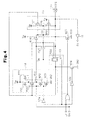
- Fig. 4 shows an input/output circuit according to a first embodiment of the present invention.
- the input/output circuit operates in an input mode and an output mode in accordance with an enable signal En and data Do.
- the enable signal En is provided to each of a NOR circuit (second logic circuit) 11, inverter circuits 12a and 12b, and the gate of an N-channel MOS transistor N21, which is included in a transfer gate 13.
- the data Do is provided to the NOR circuit 11 and the gates of a P-channel MOS transistor P21 and an N-channel MOS transistor N22, which are included in a NAND circuit (first logic circuit) 14.
- the output signal of the NOR circuit 11 is output from its output terminal and is provided to the gate of an output transistor N25, which is formed by an N-channel MOS transistor.
- the output signal of the inverter circuit 12b is provided to the gate of an N-channel MOS transistor N24.
- the source of the transistor N24 is connected to ground GND.
- the drain of the transistor N24 is connected to the gate of a P-channel MOS transistor P22, which is included in the NAND circuit 14.
- the output signal of the inverter circuit 12a is provided to the gates of an N-channel MOS transistor N23 and a P-channel MOS transistor P23, which are included in the NAND circuit 14.
- the NAND circuit 14 will now be described.
- the sources of the transistors P21 and P23 are connected to the power supply voltage V DD .
- the drains of the transistors P21 and P23 are connected to the source of the transistor P22.
- the drain of the transistor P22 is connected to the drain of the transistor N22.
- the source of the transistor N22 is connected to the drain of the transistor N23.
- the source of the transistor N23 is connected to ground GND.
- the drains of the transistors P22 and N22 are connected to an output node NN1.
- the output node NN1 functions as an output terminal of the NAND circuit 14.
- the NAND circuit 14 is in the output mode when the enable signal En has an L level.
- the L level enable signal En activates the transistor N23, inactivates the transistor P23, activates the transistor N24, and activates the transistor P22. Accordingly, the NAND circuit 14 is activated, and an inverted signal of the data Do is provided to the output node NN1.
- the NAND circuit 14 is in the input mode when the enable signal En has an H level.
- the H level enable signal En activates the transistor P23, inactivates the transistor N23, and activates the NAND circuit 14.
- the output node NN1 is connected to the gate of the output transistor P26, which is formed by the P-channel MOS transistor.
- the source of the output transistor P26 is connected to the power supply voltage V DD .
- the drain of the output transistor P26 is connected to the drain of the output transistor N25.
- the source of the output transistor N25 is connected to ground GND.
- the drains of the output transistors P26 and N25 are connected to the input/output terminal Tio.
- the transistor P26 is one example of a pull-up output transistor.
- the transistor N25 is one example of a pull-down output transistor.
- the input/output terminal Tio is connected to the transistor P22 of the NAND circuit 14 via the transfer gate 13.
- the gate of a P-channel MOS transistor P24, which is included in the transfer gate 13, is connected to the power supply voltage V DD .
- the input/output terminal Tio is connected to the output node NN1 by way of the P-channel MOS transistor P25.
- the gate of the transistor P25 is connected to the power supply voltage V DD .
- a back gate control circuit 15 is formed by P-channel MOS transistors P27 and P28.
- the source of the transistor P27 is connected to the power supply voltage V DD .
- the drain of the transistor P27 is connected to the drain of the transistor P28.
- the source of the transistor P28 is connected to the input/output terminal Tio.
- the gate of the transistor P27 is connected to the gate of the transistor P22.
- the gate of the transistor P28 is connected to the power supply voltage V DD .
- Back gate voltage VB is output from a connecting node NN2 of the drains of the transistors P27 and P28.
- the back gate voltage VB is supplied to the transistors P27 and P28 and the transistors P25, P26, P24, and P22.
- the back gate control circuit 15 is in the output mode when the enable signal En has an L level. In the output mode, the transistor N24 is activated, and the transistor P27 is activated. In this case, the transistor P28 is inactivated. Therefore, the back gate voltage VB has the same level as the power supply voltage V DD .
- the transistor N21 of the transfer gate 13 is activated when the input/output terminal Tio shifts to an L level, or ground GND level.
- the transistor P27 is activated, and the back gate voltage VB becomes equal to the power supply voltage V DD .
- the gate voltage of the transistor P27 becomes lower than the level of the power supply voltage V DD by the threshold value of the transistor N21, and the transistor P27 is maintained in the activated state.
- the transistor P24 is activated in the transfer gate 13, and the input signal VIH is applied to the transistor P27. This inactivates the transistor P27.
- the transistor P28 is activated and the back gate voltage VB becomes equal to the voltage level of the input signal VIH.
- a buffer circuit 16 is connected to the input/output terminal Tio.
- a signal provided to the input/output terminal Tio in the input mode is further provided to the internal circuit via the buffer circuit 16.
- the enable signal En shifts to an L level when entering the output mode. This inactivates the transfer gate 13 and activates the transistor N24. Further, the NAND circuit 14 is activated, the inverted signal of the data Do is output to the output node NN1, and the inverted signal of the data Do is output from the NOR circuit 11.
- either one of the output transistors P26 and N25 is activated, and an output signal that is in phase with the data Do is output from the input/output terminal Tio.
- the output transistor N25 is operated in a complementary manner with respect to the output transistor P26 in the output mode.
- the transistor P27 is activated, the transistor P28 is inactivated, and the back gate voltage VB of the power supply voltage V DD level is output.
- the enable signal En shifts to an H level when entering the input mode.
- the output signal of the NOR circuit 11 shifts to an L level. This inactivates the output transistor N25.
- the transistor P23 is activated, the transistor N23 is inactivated, the NAND circuit 14 is inactivated, and the transistor N24 is inactivated. Furthermore, the transistor N21 of the transfer gate 13 is activated.
- the gate of the transistor P27 is shifted to an L level via the transfer gate 13.
- the transistor P27 is activated. Accordingly, the back gate voltage VB having the level of the power supply voltage V DD is output from the back gate control circuit 15.
- the transistor P22 maintained in the activated state
- the output node NN1 is maintained at an H level
- the output transistor P26 is maintained in the inactivated state.
- the transistor P27 is activated, and the back gate voltage VB of the power supply voltage V DD level is output from the back gate control circuit 15.
- the transistor P25 is activated, and the gate potential at the output transistor P26 becomes equal to the voltage level of the input signal VIH.
- the output transistor P26 is maintained in the inactivated state even if the input signal VIH is applied to the input/output terminal Tio.
- a current path connecting the input/output terminal Tio, the output transistor P26, and the source of the power supply voltage V DD is not formed.
- the transistor P24 of the transfer gate 13 is activated, and the input signal VIH is applied to the gate of the transistor P22.
- the transistor P22 is inactivated. Accordingly, a current path connecting the input/output terminal Tio, the transistors P25 and P22, and the source of the power supply voltage V DD is not formed.
- the transistor N24 is inactivated. Thus, a current path connecting the input/output terminal Tio, the transistors P24 and N24, and the ground GND is also not formed.
- the transistor P27 is inactivated and the transistor P28 is activated.
- the back gate voltage VB which is equal to the voltage of the input signal VIH, is output.
- formation of PN junction diode that is, formation of a current path from the source of the power supply voltage V DD to the N-well is prevented in each of the transistors P27, P28, P25, P26, P24, and P22, which are supplied with the back gate voltage VB.
- the output transistor P26 is maintained in the inactivated state even if the input signal VIH is applied to the input/output terminal Tio. Further, a current path connecting the input/output terminal Tio, the output transistor P26, and the source of the power supply voltage V DD is not formed.
- Such an operation ensures that the transistor P25, the transfer gate 13, and the transistors P22 and P23 inactivate the output transistor P26 in the input mode.
- the transistor P25, the transfer gate 13, and the transistors P22 and P23 operate as a control circuit.
- the transistor P24 of the transfer gate 13 is activated and the input signal VIH is applied to the gate of the transistor P22.
- the transistor P22 is inactivated. Accordingly, the transistor P22 serves as a switch circuit and disconnects the output node NN1 from the power supply voltage V DD .
- a current path connecting the input terminal Tio, the transistors P25 and P22, and the source of the power supply voltage V DD is not formed.
- the transistor N24 is inactivated. Thus, the current path connecting the input/output terminal Tio, the transistors P24 and N24, and the ground GND is not formed.
- the transistor P27 is inactivated and the transistor P28 is activated when the input signal VIH is applied to the input/output terminal Tio.
- the formation of a PN junction diode that is, the formation of the current path from the source of the power supply voltage V DD to the N-well is prevented in each of the transistors P27, P28, P25, P26, 24, and P22, which are supplied with the back gate voltage VB.
- a NAND circuit 17 shown in Fig. 5 is used as the first logic circuit in lieu of the NAND circuit 14 of the first embodiment.
- the NAND circuit 17 is formed by an AND circuit 18 and an inverter circuit 19. Data Do and an inverted signal of the enable signal En are input to the AND circuit 18.
- the inverter circuit 19 includes P-channel MOS transistors P29 and P30 and an N-channel MOS transistor N26.
- the source of the transistor P29 is connected to the power supply voltage V DD .
- the drain of the transistor P29 is connected to the source of the transistor P30.
- the drain of the transistor P30 is connected to the drain of the transistor N26.
- the source of the transistor N26 is connected to ground GND.
- the output signal of the AND circuit 18 is input to the gates of the transistors P29 and N26.
- the drains of the transistors P30 and N26 are connected to the output node NN1.
- the gate of the transistor P30 is connected to the drain of the transistor N24 and connected to the input/output terminal Tio via the transfer gate 13.
- the back gate voltage VB is supplied from the back gate control circuit 15 to the back gate of the transistor P30.
- the parts other than the NAND circuit 17 are the same as the first embodiment.
- the NAND circuit 17 operates in the same manner as the NAND circuit 14 of the first embodiment. Further, only the N-channel MOS transistor N26 is arranged between the output node NN1 and ground GND. Thus, the falling speed of the output node NN1 increases, and the time required to shift the output transistor P26 from an inactivated state to an activated state is shortened. Accordingly, the operation frequency of the input/output circuit may be increased.
- a back gate control circuit 20 of Fig. 6 is used in lieu of the back gate control circuit 15 of the first embodiment.
- the back gate control circuit 20 includes P-channel MOS transistors P31 and P32.
- the back gate control circuit 20 is similar to the back gate control circuit 15 of the first embodiment except in that the gate of the transistor P31 is connected to the input/output terminal Tio.
- the back gate control circuit 20 outputs back gate voltage VB having the level of the power supply voltage V DD .
- the back gate control circuit 20 has the same advantages as the back gate control circuit 15 of the first embodiment.
- the buffer circuit 16 may be omitted from each embodiment when connecting the output terminal to a signal wire having a level that is higher than or equal to the level of the power supply voltage V DD in the high impedance state or a state in which the supply of power supply voltage V DD is suspended.
Landscapes
- Physics & Mathematics (AREA)
- Engineering & Computer Science (AREA)
- Computer Hardware Design (AREA)
- Computing Systems (AREA)
- General Engineering & Computer Science (AREA)
- Mathematical Physics (AREA)
- Logic Circuits (AREA)
Applications Claiming Priority (1)
| Application Number | Priority Date | Filing Date | Title |
|---|---|---|---|
| JP2006214546A JP4882584B2 (ja) | 2006-08-07 | 2006-08-07 | 入出力回路 |
Publications (2)
| Publication Number | Publication Date |
|---|---|
| EP1887697A2 true EP1887697A2 (de) | 2008-02-13 |
| EP1887697A3 EP1887697A3 (de) | 2008-10-01 |
Family
ID=38805634
Family Applications (1)
| Application Number | Title | Priority Date | Filing Date |
|---|---|---|---|
| EP07113863A Withdrawn EP1887697A3 (de) | 2006-08-07 | 2007-08-06 | Eingangs-/Ausgangs-Schaltung |
Country Status (4)
| Country | Link |
|---|---|
| US (1) | US7830174B2 (de) |
| EP (1) | EP1887697A3 (de) |
| JP (1) | JP4882584B2 (de) |
| KR (1) | KR100919655B1 (de) |
Cited By (1)
| Publication number | Priority date | Publication date | Assignee | Title |
|---|---|---|---|---|
| CN105656472A (zh) * | 2015-12-30 | 2016-06-08 | 中国电力科学研究院 | 一种优先权判断电路 |
Families Citing this family (6)
| Publication number | Priority date | Publication date | Assignee | Title |
|---|---|---|---|---|
| JP4557046B2 (ja) * | 2008-05-19 | 2010-10-06 | ソニー株式会社 | 出力バッファ回路および集積回路 |
| KR101993192B1 (ko) | 2012-10-04 | 2019-06-27 | 삼성전자주식회사 | 다중 전압 입력 버퍼 |
| JP2014107660A (ja) * | 2012-11-27 | 2014-06-09 | Mitsumi Electric Co Ltd | 半導体集積回路 |
| JP2016021638A (ja) | 2014-07-14 | 2016-02-04 | 株式会社ソシオネクスト | 半導体装置 |
| CN105790753B (zh) * | 2014-12-25 | 2018-12-21 | 中芯国际集成电路制造(上海)有限公司 | 输出缓冲器 |
| JP6753697B2 (ja) * | 2016-05-23 | 2020-09-09 | ローム株式会社 | Cmos出力回路 |
Family Cites Families (15)
| Publication number | Priority date | Publication date | Assignee | Title |
|---|---|---|---|---|
| JPH0435224A (ja) * | 1990-05-28 | 1992-02-06 | Nec Corp | 半導体装置 |
| US5117129A (en) * | 1990-10-16 | 1992-05-26 | International Business Machines Corporation | Cmos off chip driver for fault tolerant cold sparing |
| JP3311133B2 (ja) * | 1994-02-16 | 2002-08-05 | 株式会社東芝 | 出力回路 |
| KR0120565B1 (ko) * | 1994-04-18 | 1997-10-30 | 김주용 | 래치-업을 방지한 씨모스형 데이타 출력버퍼 |
| JP3031195B2 (ja) * | 1995-02-28 | 2000-04-10 | 株式会社日立製作所 | 入出力バッファ回路装置 |
| JP3441238B2 (ja) * | 1995-06-02 | 2003-08-25 | 株式会社東芝 | 出力回路 |
| US5543733A (en) * | 1995-06-26 | 1996-08-06 | Vlsi Technology, Inc. | High voltage tolerant CMOS input/output circuit |
| KR200216723Y1 (ko) * | 1995-07-07 | 2001-04-02 | 이구택 | 철광석 또는 원료탄의 철편 및 고결광 제거장치 |
| JP3190233B2 (ja) * | 1995-08-22 | 2001-07-23 | 株式会社東芝 | 出力バッファ回路 |
| US5844425A (en) * | 1996-07-19 | 1998-12-01 | Quality Semiconductor, Inc. | CMOS tristate output buffer with having overvoltage protection and increased stability against bus voltage variations |
| US6313672B1 (en) * | 1999-12-15 | 2001-11-06 | Exar Corporation | Over-voltage tolerant integrated circuit I/O buffer |
| US6384632B2 (en) * | 2000-02-22 | 2002-05-07 | Yamaha Corporation | Buffer circuit |
| JP3551926B2 (ja) * | 2000-02-22 | 2004-08-11 | ヤマハ株式会社 | バッファ回路 |
| KR100439041B1 (ko) * | 2002-09-25 | 2004-07-03 | 삼성전자주식회사 | 반도체 장치의 입출력 회로 |
| US6803789B1 (en) * | 2002-10-04 | 2004-10-12 | Semiconductor Manufacturing International Corporation | High voltage tolerant output buffer |
-
2006
- 2006-08-07 JP JP2006214546A patent/JP4882584B2/ja not_active Expired - Fee Related
-
2007
- 2007-08-03 US US11/882,660 patent/US7830174B2/en active Active
- 2007-08-06 EP EP07113863A patent/EP1887697A3/de not_active Withdrawn
- 2007-08-06 KR KR1020070078555A patent/KR100919655B1/ko not_active Expired - Fee Related
Cited By (2)
| Publication number | Priority date | Publication date | Assignee | Title |
|---|---|---|---|---|
| CN105656472A (zh) * | 2015-12-30 | 2016-06-08 | 中国电力科学研究院 | 一种优先权判断电路 |
| CN105656472B (zh) * | 2015-12-30 | 2018-10-16 | 中国电力科学研究院 | 一种优先权判断电路 |
Also Published As
| Publication number | Publication date |
|---|---|
| US20080030232A1 (en) | 2008-02-07 |
| KR100919655B1 (ko) | 2009-09-30 |
| JP4882584B2 (ja) | 2012-02-22 |
| EP1887697A3 (de) | 2008-10-01 |
| KR20080013759A (ko) | 2008-02-13 |
| JP2008042542A (ja) | 2008-02-21 |
| US7830174B2 (en) | 2010-11-09 |
Similar Documents
| Publication | Publication Date | Title |
|---|---|---|
| KR100309723B1 (ko) | 집적 회로 장치 | |
| US6144221A (en) | Voltage tolerant interface circuit | |
| EP1887697A2 (de) | Eingangs-/Ausgangs-Schaltung | |
| US8179160B1 (en) | Input-output (I/O) circuit supporting multiple I/O logic-level swings | |
| US10560084B2 (en) | Level shift circuit | |
| JP3759121B2 (ja) | 半導体装置 | |
| US6819159B1 (en) | Level shifter circuit | |
| JP2003229758A (ja) | 半導体装置 | |
| US20150381179A1 (en) | Signal transmission circuit suitable for ddr | |
| KR100363381B1 (ko) | 반도체 칩, 반도체 인터페이스 회로, 반도체 칩의 회로보호 방법 및 그 보호 회로 | |
| US6201428B1 (en) | 5-volt tolerant 3-volt drive push-pull buffer/driver | |
| US7859305B2 (en) | Input/output circuit | |
| EP1717955B1 (de) | Treiberschaltung | |
| US7355447B2 (en) | Level shifter circuit | |
| US20110148475A1 (en) | Driving circuit of input/output interface | |
| US7567111B2 (en) | Potential fixing circuit for integrated circuit having multiple supply potentials | |
| JP5266974B2 (ja) | 入出力回路 | |
| US7304511B2 (en) | Output circuit for interfacing between different power supply voltages | |
| US7336117B2 (en) | Enhancement of power on reliability in a dual power supply digital device with down converter | |
| US7053651B2 (en) | Low power CMOS switching | |
| JP5481071B2 (ja) | 半導体集積回路 | |
| US10541684B2 (en) | Input/output circuit | |
| US20140009187A1 (en) | Integrated circuit | |
| JP2018142894A (ja) | 出力バッファ及び半導体装置 | |
| KR101036511B1 (ko) | 입/출력 패드 장치 |
Legal Events
| Date | Code | Title | Description |
|---|---|---|---|
| PUAI | Public reference made under article 153(3) epc to a published international application that has entered the european phase |
Free format text: ORIGINAL CODE: 0009012 |
|
| AK | Designated contracting states |
Kind code of ref document: A2 Designated state(s): AT BE BG CH CY CZ DE DK EE ES FI FR GB GR HU IE IS IT LI LT LU LV MC MT NL PL PT RO SE SI SK TR |
|
| AX | Request for extension of the european patent |
Extension state: AL BA HR MK YU |
|
| PUAL | Search report despatched |
Free format text: ORIGINAL CODE: 0009013 |
|
| AK | Designated contracting states |
Kind code of ref document: A3 Designated state(s): AT BE BG CH CY CZ DE DK EE ES FI FR GB GR HU IE IS IT LI LT LU LV MC MT NL PL PT RO SE SI SK TR |
|
| AX | Request for extension of the european patent |
Extension state: AL BA HR MK RS |
|
| RAP1 | Party data changed (applicant data changed or rights of an application transferred) |
Owner name: FUJITSU MICROELECTRONICS LIMITED |
|
| 17P | Request for examination filed |
Effective date: 20090401 |
|
| AKX | Designation fees paid |
Designated state(s): DE FR |
|
| RAP1 | Party data changed (applicant data changed or rights of an application transferred) |
Owner name: FUJITSU SEMICONDUCTOR LIMITED |
|
| 17Q | First examination report despatched |
Effective date: 20140113 |
|
| RAP1 | Party data changed (applicant data changed or rights of an application transferred) |
Owner name: SOCIONEXT INC. |
|
| STAA | Information on the status of an ep patent application or granted ep patent |
Free format text: STATUS: THE APPLICATION IS DEEMED TO BE WITHDRAWN |
|
| 18D | Application deemed to be withdrawn |
Effective date: 20180301 |