EP1884983A2 - Verfahren zum Anbringen eines Klebebandes an einen Halbleiterwafer, Verfahren zum Abtrennen eines Schutzbandes von einem Halbleiterwafer und diese Verfahren verwendende Vorrichtungen - Google Patents
Verfahren zum Anbringen eines Klebebandes an einen Halbleiterwafer, Verfahren zum Abtrennen eines Schutzbandes von einem Halbleiterwafer und diese Verfahren verwendende Vorrichtungen Download PDFInfo
- Publication number
- EP1884983A2 EP1884983A2 EP07012650A EP07012650A EP1884983A2 EP 1884983 A2 EP1884983 A2 EP 1884983A2 EP 07012650 A EP07012650 A EP 07012650A EP 07012650 A EP07012650 A EP 07012650A EP 1884983 A2 EP1884983 A2 EP 1884983A2
- Authority
- EP
- European Patent Office
- Prior art keywords
- semiconductor wafer
- adhesive tape
- tape
- joining
- wafer
- Prior art date
- Legal status (The legal status is an assumption and is not a legal conclusion. Google has not performed a legal analysis and makes no representation as to the accuracy of the status listed.)
- Withdrawn
Links
Images







Classifications
-
- H—ELECTRICITY
- H10—SEMICONDUCTOR DEVICES; ELECTRIC SOLID-STATE DEVICES NOT OTHERWISE PROVIDED FOR
- H10P—GENERIC PROCESSES OR APPARATUS FOR THE MANUFACTURE OR TREATMENT OF DEVICES COVERED BY CLASS H10
- H10P72/00—Handling or holding of wafers, substrates or devices during manufacture or treatment thereof
- H10P72/04—Apparatus for manufacture or treatment
- H10P72/0442—Apparatus for placing on an insulating substrate, e.g. tape
-
- Y—GENERAL TAGGING OF NEW TECHNOLOGICAL DEVELOPMENTS; GENERAL TAGGING OF CROSS-SECTIONAL TECHNOLOGIES SPANNING OVER SEVERAL SECTIONS OF THE IPC; TECHNICAL SUBJECTS COVERED BY FORMER USPC CROSS-REFERENCE ART COLLECTIONS [XRACs] AND DIGESTS
- Y10—TECHNICAL SUBJECTS COVERED BY FORMER USPC
- Y10S—TECHNICAL SUBJECTS COVERED BY FORMER USPC CROSS-REFERENCE ART COLLECTIONS [XRACs] AND DIGESTS
- Y10S156/00—Adhesive bonding and miscellaneous chemical manufacture
- Y10S156/918—Delaminating processes adapted for specified product, e.g. delaminating medical specimen slide
- Y10S156/93—Semiconductive product delaminating, e.g. delaminating emiconductive wafer from underlayer
- Y10S156/931—Peeling away backing
-
- Y—GENERAL TAGGING OF NEW TECHNOLOGICAL DEVELOPMENTS; GENERAL TAGGING OF CROSS-SECTIONAL TECHNOLOGIES SPANNING OVER SEVERAL SECTIONS OF THE IPC; TECHNICAL SUBJECTS COVERED BY FORMER USPC CROSS-REFERENCE ART COLLECTIONS [XRACs] AND DIGESTS
- Y10—TECHNICAL SUBJECTS COVERED BY FORMER USPC
- Y10S—TECHNICAL SUBJECTS COVERED BY FORMER USPC CROSS-REFERENCE ART COLLECTIONS [XRACs] AND DIGESTS
- Y10S156/00—Adhesive bonding and miscellaneous chemical manufacture
- Y10S156/934—Apparatus having delaminating means adapted for delaminating a specified article
- Y10S156/941—Means for delaminating semiconductive product
-
- Y—GENERAL TAGGING OF NEW TECHNOLOGICAL DEVELOPMENTS; GENERAL TAGGING OF CROSS-SECTIONAL TECHNOLOGIES SPANNING OVER SEVERAL SECTIONS OF THE IPC; TECHNICAL SUBJECTS COVERED BY FORMER USPC CROSS-REFERENCE ART COLLECTIONS [XRACs] AND DIGESTS
- Y10—TECHNICAL SUBJECTS COVERED BY FORMER USPC
- Y10T—TECHNICAL SUBJECTS COVERED BY FORMER US CLASSIFICATION
- Y10T156/00—Adhesive bonding and miscellaneous chemical manufacture
- Y10T156/11—Methods of delaminating, per se; i.e., separating at bonding face
- Y10T156/1168—Gripping and pulling work apart during delaminating
-
- Y—GENERAL TAGGING OF NEW TECHNOLOGICAL DEVELOPMENTS; GENERAL TAGGING OF CROSS-SECTIONAL TECHNOLOGIES SPANNING OVER SEVERAL SECTIONS OF THE IPC; TECHNICAL SUBJECTS COVERED BY FORMER USPC CROSS-REFERENCE ART COLLECTIONS [XRACs] AND DIGESTS
- Y10—TECHNICAL SUBJECTS COVERED BY FORMER USPC
- Y10T—TECHNICAL SUBJECTS COVERED BY FORMER US CLASSIFICATION
- Y10T156/00—Adhesive bonding and miscellaneous chemical manufacture
- Y10T156/17—Surface bonding means and/or assemblymeans with work feeding or handling means
-
- Y—GENERAL TAGGING OF NEW TECHNOLOGICAL DEVELOPMENTS; GENERAL TAGGING OF CROSS-SECTIONAL TECHNOLOGIES SPANNING OVER SEVERAL SECTIONS OF THE IPC; TECHNICAL SUBJECTS COVERED BY FORMER USPC CROSS-REFERENCE ART COLLECTIONS [XRACs] AND DIGESTS
- Y10—TECHNICAL SUBJECTS COVERED BY FORMER USPC
- Y10T—TECHNICAL SUBJECTS COVERED BY FORMER US CLASSIFICATION
- Y10T156/00—Adhesive bonding and miscellaneous chemical manufacture
- Y10T156/19—Delaminating means
- Y10T156/1978—Delaminating bending means
Definitions
- the present invention relates to a method for joining a separating adhesive tape to a protective tape joined to a front face (a face on which a pattern is formed) of a semiconductor wafer (hereinafter, simply referred to as "wafer"), a method for separating the protective tape from the front face of the wafer by means of the separating adhesive tape, and apparatuses using the methods.
- a semiconductor wafer After completion of a pattern forming process, a semiconductor wafer is subjected to a back grinding process in a state that a protective tape is joined to a front face of the semiconductor wafer in order to protect a pattern. Thereafter, the protective tape is previously separated from the front face of the wafer, and then the wafer is subjected to a dicing process in which the wafer is divided into chips.
- JP-A 2002-124494 discloses one example of a technique for separating a protective tape from a front face of a wafer.
- a wafer is held by a table in a state that a front face, to which a protective tape is joined, of the wafer is directed upward.
- a separating adhesive tape is joined to the protective tape while being separated in a reverse direction.
- the protective tape joined to and integrated with the adhesive tape is separated from the front face of the wafer.
- a wafer is made thinner in response to needs for size reduction and high-density package as to an electronic device.
- a wafer made thin so as to have a thickness of several tens of micrometers becomes cracked or chipped readily due to occurrence of warpage. Consequently, there is a high possibility that such wafer is damaged in various processing and handling.
- a center of a wafer is ground in a back grinding process to form an annular convex portion at an outer periphery of a back face of the wafer; thus, the wafer is allowed to have rigidity. That is, the wafer is processed so as to be less susceptible to damage in handling.
- the annular convex portion left on the wafer brings rigidity capable of withstanding warpage. Therefore, such wafer facilitates handling without being damaged. If the wafer is held by the table in a state that a back face thereof is directed downward, however, the annular convex portion comes into contact with the table, but a flat concave portion corresponding to the center of the back face of the wafer does not come into contact with the table. Consequently, there is a problem that it is impossible to join a separating adhesive tape to a wafer, which has been made thin, with good accuracy and to separate the separating adhesive tape together with a protective tape from the wafer with good accuracy.
- An object of the present invention is to provide a method for joining a separating adhesive tape to a semiconductor wafer, a method for separating a protective tape from the semiconductor wafer, and apparatuses using these methods, each producing the following effect: it is possible to perform joining of the separating adhesive tape and separation of the protective tape using the separating adhesive tape with good accuracy without damage of the semiconductor wafer even when the semiconductor wafer has been made thin.
- the present invention adopts the following configuration:
- a method for joining a separating adhesive tape to a protective tape joined to a front face of a semiconductor wafer comprising the steps of: preparing a semiconductor wafer having a back face on which an annular convex portion is formed along an outer periphery so as to surround a back-ground area; placing the semiconductor wafer on a holding table in a state that a front face of the semiconductor wafer is directed upward and, also, allowing a locking member of the holding table to support the outer periphery of the annular convex portion such that the locking member comes into contact with the outer periphery of the annular convex portion, for securing the semiconductor wafer; supplying fluid from a side of the holding table into a space defined between the back face of the semiconductor wafer and the holding table, for increasing an internal pressure in the space; supplying a separating adhesive tape toward a surface of a protective tape joined to the front face of the semiconductor wafer; and allowing a joining member, which has a width larger than an outer diameter of the semiconductor
- a semiconductor wafer is subjected to back grinding so as to have a thickness of several tens of micrometers.
- Such semiconductor wafer is reinforced with an annular convex portion formed at an outer periphery of a back face thereof. Accordingly, it is possible to prevent the semiconductor wafer from being disadvantageously bent or warped in handling or another processing.
- a separating adhesive tape is to be joined to a protective tape joined to a front face of the semiconductor wafer
- fluid is supplied into a space defined inside the semiconductor wafer, so that a pressure in the space is appropriately increased.
- the locking member supports the outer periphery of the annular convex portion so as to come into contact with the outer periphery of the annular convex portion; thus, the wafer is tightly secured to the holding table.
- the annular convex portion has a narrow width or in a case that a flat front face of the wafer cannot be suction held.
- the width of the joining member is larger than an outer diameter of the semiconductor wafer. Therefore, a position pressed by the joining member is restricted by the annular convex portion formed along the outer periphery of the back face of the wafer placed on the holding table. That is, even when the joining member presses a thin portion of the wafer, which does not come into contact with the holding table, the wafer is prevented from being largely deformed so as to swell downward.
- an adhesive tape can be joined to, with good accuracy, the wafer which is reinforced with the annular convex portion and has an uneven thickness due to the formation of the irregularities on the back face thereof.
- the fluid is supplied into the space while an outflow of the fluid from the space is permitted, so that a pressure in the space is increased.
- a fine hole formed on the holding table permits the outflow of the fluid.
- the semiconductor wafer when the internal pressure in the space defined between the back face of the semiconductor wafer and the holding table is increased, the semiconductor wafer is deformed so as to slightly swell upward. That is, when the joining member is pressed against the semiconductor wafer from above, the semiconductor wafer is flattened. When the semiconductor wafer is flattened and then the space is reduced in volume as compared with the time when the semiconductor wafer swells upward, the internal air is discharged from the space, so that an increase in inner pressure is suppressed.
- the joining member moves slowly at an adhesive tape joining start position.
- a pressing force of the joining member to be applied to the annular convex portion corresponding to the adhesive tape joining start position is larger than a pressing force of the joining member to be applied to the flat concave portion formed inside the annular convex portion.
- the present invention also adopts the following configuration:
- a method for separating from a semiconductor wafer a protective tape joined to a front face of the semiconductor wafer comprising the steps of: preparing a semiconductor wafer having a back face on which an annular convex portion is formed along an outer periphery so as to surround a back-ground area placing the semiconductor wafer on a holding table in a state that a front face of the semiconductor wafer is directed upward and, also, allowing a locking member of the holding table to support the outer periphery of the annular convex portion such that the locking member comes into contact with the outer periphery of the annular convex portion, for securing the semiconductor wafer; supplying fluid from a side of the holding table into a space defined between the back face of the semiconductor wafer and the holding table, for increasing an internal pressure in the space; supplying a separating adhesive tape toward a surface of a protective tape joined to the front face of the semiconductor wafer; allowing a joining member, which has a width larger than an outer diameter of the semiconductor wafer,
- a semiconductor wafer is subjected to back grinding so as to have a thickness of several tens of micrometers.
- Such semiconductor wafer is reinforced with an annular convex portion formed at an outer periphery of a back face thereof. Accordingly, it is possible to prevent the semiconductor wafer from being disadvantageously bent or warped in handling or another processing.
- a separating adhesive tape is to be joined to a protective tape joined to a front face of the semiconductor wafer
- fluid is supplied into a space defined inside the semiconductor wafer, so that a pressure in the space is appropriately increased.
- the locking member supports the outer periphery of the annular convex portion so as to come into contact with the outer periphery of the annular convex portion; thus, the wafer is tightly secured to the holding table.
- the annular convex portion has a narrow width or in a case that a flat front face of the wafer cannot be suction held.
- the adhesive tape can be joined to, with good accuracy, the wafer which is reinforced with the annular convex portion and has an uneven thickness due to the formation of the irregularities on the back face thereof.
- the guide member guides the joined adhesive tape in the reverse direction; thus, the protective tape integrated with the adhesive tape is separated from the front face of the wafer.
- the semiconductor wafer is reinforced with the annular convex portion formed along the outer periphery of the back face thereof. Therefore, the semiconductor wafer is prevented from being damaged due to adhesion of the protective tape.
- the guide member is used as the joining member so that the joining of the adhesive tape to the protective tape and the separation of the protective tape from the semiconductor wafer are performed simultaneously.
- the guide member joins the adhesive tape to the surface of the protective tape while pressing the adhesive tape against the surface of the protective tape and, simultaneously, guides the adhesive tape in the reverse direction to separate the protective tape integrated with the adhesive tape from the front face of the semiconductor wafer.
- the joining of the adhesive tape to the protective tape and the separation of the protective tape from the semiconductor wafer can be performed simultaneously. This leads to reduction in processing time and simplification in configuration of an apparatus unlike a case that joining of an adhesive tape using a joining member and separation of the adhesive tape using a guide member are performed independently.
- the guide member to be used herein is made of a plate material having an edge.
- the adhesive tape integrated with the protective tape is folded back at a steep angle by the edge of the guide member. Therefore, an angle that the tape is separated from the semiconductor wafer is considerably larger than an angle in a case that a roller guides the tape in a reverse direction.
- an orthogonal component acted on the front face of the semiconductor wafer by a separating force generated at a separation point between the front face of the semiconductor wafer and the protective tape becomes small.
- the protective tape can be readily and smoothly separated from the semiconductor wafer without a large separating force to be applied to the semiconductor wafer.
- the fluid is supplied into the space while an outflow of the fluid from the space is permitted, so that a pressure in the space is increased.
- a fine hole formed on the holding table permits the outflow of the fluid.
- the semiconductor wafer when the internal pressure in the space defined between the back face of the semiconductor wafer and the holding table is increased, the semiconductor wafer is deformed so as to slightly swell upward. That is, when the joining member is pressed against the semiconductor wafer from above, the semiconductor wafer is flattened. When the semiconductor wafer is flattened and then the space is reduced in volume as compared with the time when the semiconductor wafer swells upward, the internal air is discharged from the space, so that an increase in inner pressure is suppressed.
- the joining member moves slowly at an adhesive tape joining start position.
- a pressing force of the joining member to be applied to the annular convex portion corresponding to the adhesive tape joining start position is larger than a pressing force of the joining member to be applied to the flat concave portion formed inside the annular convex portion.
- the present invention also adopts the following configuration:
- An apparatus for joining a separating adhesive tape to a protective tape joined to a front face of a semiconductor wafer comprising: a holding table for holding a semiconductor wafer, having a back face on which an annular convex portion is formed along an outer periphery so as to surround a back-ground area and a flat concave portion is formed at an inner-diameter side of the annular convex portion, so as to come into contact with the annular convex portion; a locking member for locking the outer periphery of the annular convex portion of the semiconductor wafer held by the holding table; fluid supply means for supplying fluid from a side of the holding table into a space defined between the back face of the semiconductor wafer and the holding table; tape supply means for supplying a separating adhesive tape toward a surface of a protective tape joined to the semiconductor wafer; and a tape joining unit allowing a joining member, which has a width larger than an outer diameter of the semiconductor wafer, to move from a first end to a second end
- examples of the locking member may include : locking pins provided in a pair of clamp members disposed so as to be opposite to each other with the semiconductor wafer interposed therebetween and moved so as to approach each other or so as to be spaced away from each other; and a pair of locking members each having a "V"-shaped recess, the locking members being disposed so as to be opposite to each other with the semiconductor wafer interposed therebetween and moved so as to approach each other or so as to be spaced away from each other.
- the present invention also adopts the following configuration:
- An apparatus for separating from a semiconductor wafer a protective tape joined to a front face of the semiconductor wafer comprising: a holding table for holding the semiconductor wafer, having a back face on which an annular convex portion is formed along an outer periphery so as to surround a back-ground area and a flat concave portion is formed at an inner-diameter side of the annular convex portion, so as to come into contact with the annular convex portion; a locking member for locking the outer periphery of the annular convex portion of the semiconductor wafer held by the holding table; fluid supply means for supplying fluid from a side of the holding table into a space defined between the back face of the semiconductor wafer and the holding table; tape supply means for supplying a separating adhesive tape toward a surface of a protective tape joined to the semiconductor wafer; a tape joining unit allowing a joining member, which has a width larger than an outer diameter of the semiconductor wafer, to move from a first end to a second end of the semiconductor
- examples of the locking member may include: locking pins provided in a pair of clamp members disposed so as to be opposite to each other with the semiconductor wafer interposed therebetween and moved so as to approach each other or so as to be spaced away from each other; and a pair of locking members each having a "V"-shaped recess, the locking members being disposed so as to be opposite to each other with the semiconductor wafer interposed therebetween and moved so as to approach each other or so as to be spaced away from each other.
- an apparatus capable of realizing a method for joining an adhesive tape to a semiconductor wafer and a method for separating a protective tape from the semiconductor wafer.
- Fig. 1 is a perspective view illustrating a general configuration of an apparatus for separating a protective tape from a semiconductor wafer as one example of the apparatus executing the method according to the present invention.
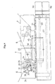
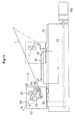
- Fig. 2 is a front view illustrating the general configuration of the apparatus.
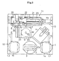
- Fig. 3 is a plan view illustrating the general configuration of the apparatus.
- a wafer supply section 1 In the adhesive tape joining/separation apparatus, a wafer supply section 1, a wafer transport mechanism 3, an alignment stage 4, a tape supply section 5, a holding table 6, a tape joining unit 7, a tape separation unit 8, a tape collection section 9, a wafer collection section 10, a unit driving section 11 and the like are provided on a base 12.
- the wafer supply section 1 includes a cassette C1 for housing wafers W, each of which has been subjected to a back grinding process, in a stacked manner.
- the wafer transport mechanism 3 is equipped with a robot arm 2.
- the alignment stage 4 performs alignment on the wafer W.
- the tape supply section 5 supplies a separating adhesive tape T toward a site where a separating process is performed.
- the holding table 6 suction holds the wafer W.
- the tape joining unit 7 joins the adhesive tape T to the wafer W on the holding table 6.
- the tape separation unit 8 separates the joined adhesive tape T.
- the tape collection section 9 reels and collects the adhesive tape Ts subjected to the separating process.
- the wafer collection section 10 includes a cassette C2 for housing the wafers W, each of which has been subjected to the separating process, in a stacked manner.
- the unit driving section 11 allows the tape joining unit 7 and the tape separation unit 8 to independently reciprocate laterally.
- the wafer supply section 1, the wafer transport mechanism 3, the alignment stage 4, the holding table 6 and the wafer collection section 10 are disposed at a top side of the base 12.
- the tape supply section 5 and the tape collection section 9 are disposed at a front side of a vertical wall 13 which is provided upright on the top side of the base 12.
- the tape joining unit 7 and the tape separation unit 8 are directed to an opening formed below the vertical wall 13.
- the unit driving section 11 is disposed at a rear side of the vertical wall 13.
- wafers W in a horizontal posture are inserted into and housed in the cassette C1 with an appropriate clearance vertically interposed therebetween in a state that a front face of each wafer W, to which an ultraviolet-ray curable protective tape PT is joined, is directed upward.
- the cassette C1 is mounted on a cassette bench 14 with the wafers W inserted thereinto and housed therein. As illustrated in Fig. 3, the cassette bench 14 is turnable by an air cylinder 15 such that a direction thereof is changed.
- wafers W in a horizontal posture are inserted into and housed in the cassette C2 with an appropriate clearance vertically interposed therebetween in a state that a protective tape PT is separated from each wafer W, and the cassette C2 is mounted on a cassette bench 16 with the wafers W inserted thereinto and housed therein.
- the cassette bench 16 is also turnable by an air cylinder 17 such that a direction thereof is changed.
- the wafer W is irradiated with ultraviolet rays before being housed in the cassette C1 such that an adhesive surface of the protective tape PT is lowered in adhesion.
- a wafer W which is a subject to be processed is subjected to a back grinding process in a state that a protective tape PT is joined to a front face (a face on which a pattern is formed) thereof as illustrated in Fig. 7 which is a perspective view illustrating the front face of the wafer W, Fig. 8 which is a perspective view illustrating a back face of the wafer W and Fig. 9 which is a sectional view illustrating the wafer W.
- the back face of the wafer W is ground such that an outer periphery is higher than a ground area by about 2 mm in a radial direction. More specifically, a flat concave portion 40 is formed on the back face and an annular convex portion 41 is left along the outer periphery of the back face.
- the flat concave portion 40 has a depth d of several hundreds of micrometers and a thickness t of several tens of micrometers, for example. That is, the annular convex portion 41 formed at the outer periphery of the back face functions as an annular rib for enhancing rigidity of the wafer W. Accordingly, the annular convex portion 41 hinders the wafer W from being warped in handling or another processing.
- the robot arm 2 of the transport mechanism 3 is advanceable/retreatable horizontally, is turnable and is movable vertically.
- the robot arm 2 has a tip end provided with a suction holding part 2a formed into a horse-shoe shape.
- the robot arm 2 takes a wafer W out of the wafer supply section 1, supplies the wafer W to the alignment stage 4, transports the wafer W from the alignment stage 4 to the holding table 6, carries the processed wafer W out of the holding table 6, and carries the processed wafer W in the wafer collection section 10.
- the tape supply section 5 guides a separating adhesive tape T, which is unreeled from an original tape roll TR, toward the tape joining unit 7 and the tape separation unit 8 via a position above the holding table 6.
- a width of the adhesive tape T to be used herein is smaller than a diameter of a wafer W.
- a suction pad 18 for giving or receiving a wafer W is provided at a center of a top side of the holding table 6 for holding the wafer W placed thereon in separation of a protective tape, so as to protrude from or retreat into the holding table 6. Further, a pair of front and rear clamp members 42 are attached to the holding table 6 so as to be slidable in a forward/rearward direction.
- the suction pad 18 when a vacuum pump (not illustrated) communicated with and connected to the suction pad 18 at an upstream side is operated so as to generate a positive pressure, air is supplied via a channel 19 to a space S defined between the holding table 6 and the annular convex portion 41 of the wafer W.
- the space S is applied with a predetermined pressure which is slightly higher than an atmospheric pressure.
- the holding table 6 is provided with a fine hole (not illustrated) which permits internal air with appropriate resistance to flow externally from the space S when the space S is applied with the pressure.
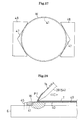
- each clamp member 42 includes a pair of locking pins 45 provided at a right side and a left side thereof. Each locking pin 45 protrudes from the holding table 6 so as to be lower than a thickness of a wafer W, through a longitudinally oval hole 46 formed on the holding table 6. It is to be noted that the locking pin 45 corresponds to a locking member according to the present invention.
- the tape joining unit 7 has the following structure. That is, a movable bench 22 is supported on a rail 21 so as to move laterally along the rail 21, and is allowed to reciprocate laterally and horizontally at a fixed stroke through a feed screw 23 which is driven by a motor M1 in a forward/backward direction. Further, the movable bench 22 is equipped with a joining roller 25 which is movable vertically through an oscillation arm 24. A width of the joining roller 25 to be used herein is larger than an outer diameter of a wafer W. It is to be noted that the joining roller 25 corresponds to a joining member according to the present invention.
- the tape separation unit 8 has the following structure. That is, a movable bench 26 is supported on the rail 21 so as to move laterally along the rail 21, and is allowed to reciprocate laterally and horizontally at a fixed stroke through a feed screw 27 which is driven by a motor M2 in a forward/backward direction.
- the movable bench 26 is equipped with a tape separating guide member 28, a guide roller 29, a feed roller 30 which is rotatably driven, and a nip roller 31 which is opposite to the feed roller 30.
- the tape separating guide member 28 is formed into a plate shape.
- a tip end of the guide member 28 is formed into a sharp edge, and a width of the guide member 28 is larger than an outer diameter of a wafer W.
- the guide member 28 is fixedly coupled to a rotational support shaft 32 through a slit 33 and a bolt 34 such that advancement or retreat of the guide member 28 is adjustable.
- the rotational support shaft 32 is rotatably supported at the front side of the movable bench 26.
- an operating arm 35 is fastened to and coupled to a base end of the rotational support shaft 32.
- a coupling rod 37 is pivotally supported on and coupled to a free end of the operating arm 35, and is coupled to an air cylinder 36 which is attached to the front side of the movable bench 26.
- the rotational support shaft 32 is rotated by oscillation of the operating arm 35 caused by advancement or retreat of the air cylinder 36. With this operation, the tip end edge of the guide member 28 moves upward/downward.
- a coupling rod 37 is extended from the free end of the operating arm 35, and is screwed into and attached to a piston rod 36a of the air cylinder 36.
- the robot arm 2 is inserted into the cassette C1 of the wafer supply section 1, suction holds a back face of a predetermined wafer W, takes the wafer W out of the cassette C1, and transfers the wafer W to the alignment stage 4.
- the alignment stage 4 performs alignment on the wafer W on the basis of detection of a detection site such as a notch previously formed at an outer periphery of the wafer W.
- the robot arm 2 suction holds the back face of the wafer W again, and transports the wafer W to the holding table 6 which moves downward to a wafer reception level on standby.
- the suction pad 18 protrudes from the holding table 6 to receive the wafer W. Then, the suction pad 18 moves downward, so that the wafer W is placed on the holding table 6.
- the clamp members 42 illustrated in Fig. 11 are situated on standby at positions which are opposite to each other with a predetermined clearance interposed therebetween, and the wafer W is placed on the clearance between the front and rear locking pines 45.
- the both clamp members 42 move so as to approach each other.
- the locking pins 45 of each clamp member 42 come into contact with the outer periphery of the wafer W, so that predetermined clamping forces are applied to the wafer W at the center of the holding table 6 from left and right sides.
- the locking pins 45 lock and secure the wafer W.
- the vacuum pump When the wafer W is locked and secured on the holding table 6, the vacuum pump operates so as to generate a positive pressure; thus, air is supplied into a space S defined between the wafer W and the holding table 6. Thus, the space S is applied with a predetermined pressure which is slightly higher than an atmospheric pressure.
- the tape joining unit 7 and the tape separation unit 8 are situated at standby positions, respectively, which are spaced away from the holding table 6 in a rearward direction.
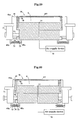
- the width of the joining roller 25 to be used herein is larger than an outer diameter of the wafer W. Therefore, a force that the joining roller 25 presses the wafer W placed on the holding table 6 is restricted by the outer periphery of the back face of the wafer W. Accordingly, the thin portion of the wafer W pressed from above is prevented from being deformed by the joining roller 25 so as to swell downward.
- the air cylinder 36 protrudes to its stroke end and the guide member 28 moves downward to the lower limit position by the oscillation of the operating arm 35.
- the tip end of the guide member 28 moves while pressing the adhesive tape T against the surface of the protective PT and, also, the feed roller 30 feeds the adhesive tape T at a circumferential speed which is in synchronization with the moving speed of the guide member 28. Accordingly, the adhesive tape T is folded by the tip end of the guide member 28 in a reverse direction at a folding angle ⁇ , and then is guided into between the feed roller 30 and the nip roller 31 through the guide roller 29. As illustrated in Figs. 6 and 17, then, the adhesive tape T travels with the protective tape PT integrated therewith, so that the protective tape PT is separated from the front face of the wafer W.
- the folding angle ⁇ of the adhesive tape T by the guide member 28 is set at a large angle, for example, 90° or more, preferably 100° or more.
- the aforementioned operation may be implemented by the folding angle ⁇ of less than 90° (approximate to 90°) depending on conditions such as a viscosity of the adhesive tape T, an elasticity of the adhesive tape T and a strength of the wafer W.
- the folding angle ⁇ of the adhesive tape T is set to be smaller as the elasticity of the adhesive tape T is higher. This setting can be performed in such a manner that an angle of the guide member 28 situated at the lower limit position is adjusted by expansion/contraction of the coupling rod 37.
- a change in height of the guide member 28 in response to the change in angle of the guide member 28 can be corrected by adjustment of an attachment position of the guide member 28 to the rotational support shaft 32.
- a forward moving speed of the guide member 28 is made slow when the guide member 28 passes by the end of the wafer W to start separation of the protective tape PT and, thereafter, such forward moving speed is made fast.
- the feed roller 30 is rotatably driven by a driving device (not illustrated) through a slip clutch which idles by a load exceeding predetermined torque. Therefore, the feed roller 30 feeds the adhesive tape T while applying a predetermined tension to the adhesive tape T.
- the clamp members 42 are moved so as to be spaced away from each other to release grasp of the outer periphery of the wafer W by the locking pins 45, and then the suction pad 18 lifts up the wafer W. Thereafter, the robot arm 2 transports the wafer W from the holding table 6 to the wafer collection section 10. Herein, the wafer W is inserted into and housed in the cassette C2.
- the tape joining unit 7 and the tape separation unit 8 return to the respective standby positions and, also, the tape collection section 9 reels and collects the adhesive tape Ts subjected to the separating process.
- the joining roller 25 and the guide member 28 move upward to standby positions, respectively.
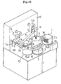
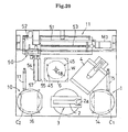
- Figs. 18 to 26 illustrate an apparatus according to a second embodiment of the present invention, that is, an apparatus for separating a protective tape from a semiconductor wafer.
- a tape joining/separation unit 50 is provided in place of the tape joining unit 7 and the tape separation unit 8 in the first embodiment.
- the tape joining/separation unit 50 has the following structure. That is, a movable bench 52 is supported on a pair of front and rear rails 51 so as to slidably move laterally along the pair of rails 51, and is allowed to move laterally and horizontally through a feed screw 53 which is driven by a motor M3 in a forward/backward direction.
- the movable bench 52 is equipped with a guide member 54 which also serves as a joining member, a guide roller 55, a feed roller 56 which is rotatably driven, and a nip roller 57 which is opposite to the feed roller 56.
- the guide member 54 of the tape joining/separation unit 50 is formed into a plate shape.
- a tip end of the guide member 54 is formed into a sharp edge, and a width of the guide member 54 is larger than an outer diameter of a wafer W.
- the guide member 54 is fixedly coupled to a rotational support shaft 58 which is rotatably supported at a front side of the movable bench 52 such that a forward/rearward position thereof is adjustable.
- an operating arm 59 is fastened to and coupled to a base end of the rotational support shaft 58. Further, a free end of the operating arm 59 is coupled to an air cylinder 61 which is attached to the front side of the movable bench 52.
- the rotational support shaft 58 is rotated by oscillation of the operating arm 59 caused by expansion/contraction of the air cylinder 61. With this operation, the tip end of the guide member 54 moves upward/downward.
- the wafer W is held on the holding table 6, and then a space S defined between the wafer W and the holding table 6 is increased in internal pressure.
- the tape joining/separation unit 50 moves forward to a position above the wafer W. More specifically, the tape joining/separation unit 50 moves forward such that the tip end of the guide member 54 reaches a forward point spaced away from a circumferential end of the wafer W on a standby position side by an appropriate distance.
- the air cylinder 61 protrudes to its stroke end, and the guide member 54 is allowed to move downward to a lower limit position by an operation of the operating arm 59. That is, the tip end of the guide member 54 comes into contact with a surface (non-adhesive surface) of an adhesive tape T, and then presses the adhesive tape T against a surface of a protective tape PT.
- the tape joining/separation unit 50 moves rearward to its standby position. That is, the tip end of the guide member 54 joins the adhesive tape T to the surface of the protective tape PT while pressing the adhesive tape T against the protective tape PT.
- the tape joining/separation unit 50 moves forward in a reverse direction.
- the tip end of the guide member 54 moves while pressing the adhesive tape T against the surface of the protective tape PT, and the feed roller 56 reels the adhesive tape T at a circumferential speed which is in synchronization with the moving speed of the guide member 54.
- the protective tape PT joined to and integrated with the adhesive tape T is separated from the front face of the wafer W together with the adhesive tape T.
- a robot arm 2 transports the wafer W from the holding table 6 to a wafer collection section 10.
- the wafer W is inserted into and housed in a cassette C2.
- the tape joining/separation unit 50 returns to its standby position and, also, a tape collection section 9 reels and collects the adhesive tape Ts subjected to the separating process.
- the guide member 54 moves upward to its standby position.
- the apparatus according to each of the aforementioned embodiments produces the following advantages. That is, even in a case of using a wafer W with surface irregularities, which has an annular convex portion 41 formed along an outer periphery of a back face so as to surround a back-ground area, when a separating adhesive tape T is joined to a protective tape PT joined to a front face of the wafer W, a space S defined inside the wafer W is pressurized appropriately with air supplied thereinto.
- a width of the annular convex portion 41 coming into contact with the holding table 6 is small. Therefore, even when a suction force cannot withstand a pressure applied to the space S, the locking pins 45 come into contact with the outer periphery of the wafer W, thereby locking and securing the wafer W on the holding table 6 by left and right predetermined grasping forces. Therefore, it is possible to prevent the air from being leaked from the space S and to hold the wafer W. In addition, even when the thin portion of the wafer W is pressed from above, the wafer is prevented from being largely deformed so as to swell downward.
- the present invention may be modified variously as follows.
Landscapes
- Container, Conveyance, Adherence, Positioning, Of Wafer (AREA)
- Mechanical Treatment Of Semiconductor (AREA)
Applications Claiming Priority (1)
| Application Number | Priority Date | Filing Date | Title |
|---|---|---|---|
| JP2006208119A JP4711904B2 (ja) | 2006-07-31 | 2006-07-31 | 半導体ウエハへの粘着テープ貼付け方法および半導体ウエハからの保護テープ剥離方法 |
Publications (1)
| Publication Number | Publication Date |
|---|---|
| EP1884983A2 true EP1884983A2 (de) | 2008-02-06 |
Family
ID=38327057
Family Applications (1)
| Application Number | Title | Priority Date | Filing Date |
|---|---|---|---|
| EP07012650A Withdrawn EP1884983A2 (de) | 2006-07-31 | 2007-06-28 | Verfahren zum Anbringen eines Klebebandes an einen Halbleiterwafer, Verfahren zum Abtrennen eines Schutzbandes von einem Halbleiterwafer und diese Verfahren verwendende Vorrichtungen |
Country Status (6)
| Country | Link |
|---|---|
| US (1) | US7857029B2 (de) |
| EP (1) | EP1884983A2 (de) |
| JP (1) | JP4711904B2 (de) |
| KR (1) | KR101312908B1 (de) |
| CN (1) | CN101118843B (de) |
| TW (1) | TWI425564B (de) |
Cited By (2)
| Publication number | Priority date | Publication date | Assignee | Title |
|---|---|---|---|---|
| EP1821335A3 (de) * | 2006-02-13 | 2009-03-25 | Tokyo Seimitsu Co.,Ltd. | Waferverarbeitungsvorrichtung |
| EP2445001A3 (de) * | 2010-10-19 | 2016-03-23 | Nitto Denko Corporation | Vorrichtung und Verfahren zur Trennung von Schutzband |
Families Citing this family (23)
| Publication number | Priority date | Publication date | Assignee | Title |
|---|---|---|---|---|
| JP5093849B2 (ja) * | 2008-06-26 | 2012-12-12 | リンテック株式会社 | シート剥離装置及び剥離方法 |
| JP5292057B2 (ja) * | 2008-10-30 | 2013-09-18 | リンテック株式会社 | テーブル及びこれを用いたシート剥離装置並びに剥離方法 |
| JP5201511B2 (ja) * | 2009-01-19 | 2013-06-05 | 株式会社タカトリ | ウエハの保持テーブル |
| JP2010186972A (ja) * | 2009-02-13 | 2010-08-26 | Disco Abrasive Syst Ltd | ウエーハの加工方法 |
| JP2010186971A (ja) * | 2009-02-13 | 2010-08-26 | Disco Abrasive Syst Ltd | ウエーハの加工方法 |
| JP5442288B2 (ja) * | 2009-03-27 | 2014-03-12 | 日東電工株式会社 | 保護テープ剥離方法およびこれを用いた保護テープ剥離装置 |
| JP5417131B2 (ja) * | 2009-11-20 | 2014-02-12 | 日東電工株式会社 | 粘着テープ貼付け装置および粘着テープ貼付け方法 |
| US8574398B2 (en) | 2010-05-27 | 2013-11-05 | Suss Microtec Lithography, Gmbh | Apparatus and method for detaping an adhesive layer from the surface of ultra thin wafers |
| JP2012004290A (ja) * | 2010-06-16 | 2012-01-05 | Lintec Corp | シート剥離装置及び剥離方法 |
| JP2012164839A (ja) * | 2011-02-08 | 2012-08-30 | Lintec Corp | 板状部材の支持装置及び支持方法、並びに、シート剥離装置及び剥離方法 |
| JP5825511B2 (ja) * | 2011-06-13 | 2015-12-02 | 株式会社東京精密 | 半導体基板の切断方法 |
| JP5977024B2 (ja) * | 2011-12-26 | 2016-08-24 | 日東電工株式会社 | 保護テープ剥離方法および保護テープ剥離装置 |
| JP6099118B2 (ja) * | 2012-04-26 | 2017-03-22 | Necエンジニアリング株式会社 | シート貼付システム及びシート貼付方法 |
| JP6189700B2 (ja) * | 2013-10-03 | 2017-08-30 | 株式会社ディスコ | ウエーハの加工方法 |
| CN104319240B (zh) * | 2014-10-27 | 2017-06-23 | 京东方科技集团股份有限公司 | 一种柔性基板贴附方法 |
| JP6375209B2 (ja) * | 2014-11-10 | 2018-08-15 | 日東電工株式会社 | 粘着テープ貼付け方法および粘着テープ貼付け装置 |
| JP7146457B2 (ja) * | 2018-05-31 | 2022-10-04 | 日東電工株式会社 | 粘着テープ剥離方法および粘着テープ剥離装置 |
| JP7285635B2 (ja) * | 2018-12-03 | 2023-06-02 | 株式会社ディスコ | テープ剥離装置及び研削装置 |
| WO2020172785A1 (en) | 2019-02-26 | 2020-09-03 | Yangtze Memory Technologies Co., Ltd. | Method and device for wafer taping |
| US12103288B2 (en) * | 2019-03-27 | 2024-10-01 | Mitsui Chemicals Tohcello, Inc. | Affixing device |
| JP7658747B2 (ja) * | 2020-03-30 | 2025-04-08 | 日東電工株式会社 | デバイス封止方法、デバイス封止装置、および半導体製品の製造方法 |
| TWI883179B (zh) * | 2020-06-09 | 2025-05-11 | 日商日東電工股份有限公司 | 黏著片貼附方法、黏著片貼附裝置及半導體製品的製造方法 |
| CN114132043B (zh) * | 2021-12-09 | 2023-03-24 | 深圳市华星光电半导体显示技术有限公司 | 贴膜装置 |
Family Cites Families (16)
| Publication number | Priority date | Publication date | Assignee | Title |
|---|---|---|---|---|
| JPS63166243A (ja) * | 1986-12-27 | 1988-07-09 | Mitsubishi Electric Corp | 半導体ウエハのテ−プ貼付装置 |
| JP2911997B2 (ja) * | 1989-10-20 | 1999-06-28 | 日本電気株式会社 | 半導体ウェハーへのテープ貼付装置 |
| JPH05114644A (ja) * | 1991-10-23 | 1993-05-07 | Nikon Corp | 基板の位置決め装置 |
| JPH05121384A (ja) * | 1991-10-25 | 1993-05-18 | Nec Kansai Ltd | 半導体装置の製造方法 |
| JP2655975B2 (ja) * | 1992-09-18 | 1997-09-24 | 三菱マテリアル株式会社 | ウェーハ研磨装置 |
| JPH09266242A (ja) * | 1996-03-27 | 1997-10-07 | Kuroda Precision Ind Ltd | 吸着用チャック装置 |
| US5821166A (en) * | 1996-12-12 | 1998-10-13 | Komatsu Electronic Metals Co., Ltd. | Method of manufacturing semiconductor wafers |
| JPH1174164A (ja) * | 1997-08-27 | 1999-03-16 | Canon Inc | 基板処理装置、基板支持装置及び基板処理方法並びに基板の製造方法 |
| JP4502547B2 (ja) * | 2000-08-07 | 2010-07-14 | 日東電工株式会社 | 半導体ウエハの保護テープ除去方法およびその装置 |
| KR100856596B1 (ko) * | 2001-06-11 | 2008-09-03 | 닛토덴코 가부시키가이샤 | 반도체 웨이퍼의 불요물 제거방법 및 그 장치 |
| JP4058482B2 (ja) * | 2002-04-11 | 2008-03-12 | レーザーテック株式会社 | 基板保持装置 |
| JP2004266212A (ja) * | 2003-03-04 | 2004-09-24 | Tadahiro Omi | 基板の処理システム |
| JP2005175384A (ja) * | 2003-12-15 | 2005-06-30 | Nitto Denko Corp | 保護テープの貼付方法及び剥離方法 |
| JP2006100728A (ja) * | 2004-09-30 | 2006-04-13 | Nitto Denko Corp | 保護テープ剥離方法およびこれを用いた装置 |
| JP2006186023A (ja) * | 2004-12-27 | 2006-07-13 | Nec Electronics Corp | ウェハ把持具およびウェハ移載装置 |
| JP4791774B2 (ja) * | 2005-07-25 | 2011-10-12 | 株式会社ディスコ | ウェーハの加工方法及び研削装置 |
-
2006
- 2006-07-31 JP JP2006208119A patent/JP4711904B2/ja active Active
-
2007
- 2007-06-28 EP EP07012650A patent/EP1884983A2/de not_active Withdrawn
- 2007-07-25 TW TW096127012A patent/TWI425564B/zh not_active IP Right Cessation
- 2007-07-27 US US11/878,823 patent/US7857029B2/en not_active Expired - Fee Related
- 2007-07-30 CN CN2007101437078A patent/CN101118843B/zh not_active Expired - Fee Related
- 2007-07-30 KR KR1020070076129A patent/KR101312908B1/ko not_active Expired - Fee Related
Cited By (2)
| Publication number | Priority date | Publication date | Assignee | Title |
|---|---|---|---|---|
| EP1821335A3 (de) * | 2006-02-13 | 2009-03-25 | Tokyo Seimitsu Co.,Ltd. | Waferverarbeitungsvorrichtung |
| EP2445001A3 (de) * | 2010-10-19 | 2016-03-23 | Nitto Denko Corporation | Vorrichtung und Verfahren zur Trennung von Schutzband |
Also Published As
| Publication number | Publication date |
|---|---|
| JP4711904B2 (ja) | 2011-06-29 |
| TWI425564B (zh) | 2014-02-01 |
| KR20080012186A (ko) | 2008-02-11 |
| KR101312908B1 (ko) | 2013-09-30 |
| CN101118843B (zh) | 2012-01-25 |
| TW200814177A (en) | 2008-03-16 |
| JP2008034710A (ja) | 2008-02-14 |
| US7857029B2 (en) | 2010-12-28 |
| CN101118843A (zh) | 2008-02-06 |
| US20080023134A1 (en) | 2008-01-31 |
Similar Documents
| Publication | Publication Date | Title |
|---|---|---|
| US7857029B2 (en) | Method for joining adhesive tape to semiconductor wafer, method for separating protective tape from semiconductor wafer, and apparatuses using the methods | |
| US7763141B2 (en) | Method for joining adhesive tape to semiconductor wafer, method for separating protective tape from semiconductor wafer, and apparatuses using the methods | |
| US7850799B2 (en) | Method for affixing adhesive tape to semiconductor wafer, and apparatus using the same | |
| US7719125B2 (en) | Method for detaching a semiconductor chip from a foil and device for mounting semiconductor chips | |
| US6919284B2 (en) | Protective tape applying method and apparatus, and protective tape separating method | |
| US7470120B2 (en) | Configurable die detachment apparatus | |
| US20100038009A1 (en) | Method and apparatus for joining protective tape to semiconductor wafer | |
| US8679289B2 (en) | Method and apparatus for separating protective tape | |
| US7135081B2 (en) | Adhesive tape applying method and apparatus | |
| EP1320121A2 (de) | Verfahren und Vorrichtung zum Transport von Halbleiterwafern | |
| JP2005175384A (ja) | 保護テープの貼付方法及び剥離方法 | |
| JP7240440B2 (ja) | 粘着テープ貼付け方法および粘着テープ貼付け装置 | |
| CN112992761A (zh) | 片状粘合材料剥离装置 | |
| KR100674077B1 (ko) | 천공 장치 | |
| US12122135B2 (en) | Sheet peeling method and sheet peeling apparatus using peeling tool | |
| JP4515041B2 (ja) | ウェーハシートのエキスパンド装置 | |
| WO2023188163A1 (ja) | ウェハ拡張装置及び部品供給装置 | |
| CN118692950A (zh) | 片剥离装置 |
Legal Events
| Date | Code | Title | Description |
|---|---|---|---|
| PUAI | Public reference made under article 153(3) epc to a published international application that has entered the european phase |
Free format text: ORIGINAL CODE: 0009012 |
|
| AK | Designated contracting states |
Kind code of ref document: A2 Designated state(s): AT BE BG CH CY CZ DE DK EE ES FI FR GB GR HU IE IS IT LI LT LU LV MC MT NL PL PT RO SE SI SK TR |
|
| AX | Request for extension of the european patent |
Extension state: AL BA HR MK YU |
|
| STAA | Information on the status of an ep patent application or granted ep patent |
Free format text: STATUS: THE APPLICATION IS DEEMED TO BE WITHDRAWN |
|
| 18D | Application deemed to be withdrawn |
Effective date: 20100105 |