EP1820372B1 - Lichtemittierendes bauelement - Google Patents
Lichtemittierendes bauelement Download PDFInfo
- Publication number
- EP1820372B1 EP1820372B1 EP05787887.8A EP05787887A EP1820372B1 EP 1820372 B1 EP1820372 B1 EP 1820372B1 EP 05787887 A EP05787887 A EP 05787887A EP 1820372 B1 EP1820372 B1 EP 1820372B1
- Authority
- EP
- European Patent Office
- Prior art keywords
- light
- layer
- electrode
- substance
- emitting
- Prior art date
- Legal status (The legal status is an assumption and is not a legal conclusion. Google has not performed a legal analysis and makes no representation as to the accuracy of the status listed.)
- Active
Links
- 239000000126 substance Substances 0.000 claims description 94
- 229910000476 molybdenum oxide Inorganic materials 0.000 claims description 40
- IBHBKWKFFTZAHE-UHFFFAOYSA-N n-[4-[4-(n-naphthalen-1-ylanilino)phenyl]phenyl]-n-phenylnaphthalen-1-amine Chemical group C1=CC=CC=C1N(C=1C2=CC=CC=C2C=CC=1)C1=CC=C(C=2C=CC(=CC=2)N(C=2C=CC=CC=2)C=2C3=CC=CC=C3C=CC=2)C=C1 IBHBKWKFFTZAHE-UHFFFAOYSA-N 0.000 claims description 40
- PQQKPALAQIIWST-UHFFFAOYSA-N oxomolybdenum Chemical compound [Mo]=O PQQKPALAQIIWST-UHFFFAOYSA-N 0.000 claims description 31
- 229910044991 metal oxide Inorganic materials 0.000 claims description 29
- 150000004706 metal oxides Chemical class 0.000 claims description 29
- 150000002894 organic compounds Chemical class 0.000 claims description 29
- AMGQUBHHOARCQH-UHFFFAOYSA-N indium;oxotin Chemical compound [In].[Sn]=O AMGQUBHHOARCQH-UHFFFAOYSA-N 0.000 claims description 9
- VYPSYNLAJGMNEJ-UHFFFAOYSA-N Silicium dioxide Chemical compound O=[Si]=O VYPSYNLAJGMNEJ-UHFFFAOYSA-N 0.000 claims description 7
- 229910052814 silicon oxide Inorganic materials 0.000 claims description 7
- XHCLAFWTIXFWPH-UHFFFAOYSA-N [O-2].[O-2].[O-2].[O-2].[O-2].[V+5].[V+5] Chemical compound [O-2].[O-2].[O-2].[O-2].[O-2].[V+5].[V+5] XHCLAFWTIXFWPH-UHFFFAOYSA-N 0.000 claims description 6
- 229910001935 vanadium oxide Inorganic materials 0.000 claims description 6
- IYZMXHQDXZKNCY-UHFFFAOYSA-N 1-n,1-n-diphenyl-4-n,4-n-bis[4-(n-phenylanilino)phenyl]benzene-1,4-diamine Chemical compound C1=CC=CC=C1N(C=1C=CC(=CC=1)N(C=1C=CC(=CC=1)N(C=1C=CC=CC=1)C=1C=CC=CC=1)C=1C=CC(=CC=1)N(C=1C=CC=CC=1)C=1C=CC=CC=1)C1=CC=CC=C1 IYZMXHQDXZKNCY-UHFFFAOYSA-N 0.000 claims description 4
- 239000007983 Tris buffer Substances 0.000 claims description 4
- 239000003086 colorant Substances 0.000 claims description 4
- YRZZLAGRKZIJJI-UHFFFAOYSA-N oxyvanadium phthalocyanine Chemical compound [V+2]=O.C12=CC=CC=C2C(N=C2[N-]C(C3=CC=CC=C32)=N2)=NC1=NC([C]1C=CC=CC1=1)=NC=1N=C1[C]3C=CC=CC3=C2[N-]1 YRZZLAGRKZIJJI-UHFFFAOYSA-N 0.000 claims description 4
- 230000001747 exhibiting effect Effects 0.000 claims description 3
- DYIZHKNUQPHNJY-UHFFFAOYSA-N oxorhenium Chemical compound [Re]=O DYIZHKNUQPHNJY-UHFFFAOYSA-N 0.000 claims description 3
- IEQIEDJGQAUEQZ-UHFFFAOYSA-N phthalocyanine Chemical compound N1C(N=C2C3=CC=CC=C3C(N=C3C4=CC=CC=C4C(=N4)N3)=N2)=C(C=CC=C2)C2=C1N=C1C2=CC=CC=C2C4=N1 IEQIEDJGQAUEQZ-UHFFFAOYSA-N 0.000 claims description 3
- 229910003449 rhenium oxide Inorganic materials 0.000 claims description 3
- OGGKVJMNFFSDEV-UHFFFAOYSA-N 3-methyl-n-[4-[4-(n-(3-methylphenyl)anilino)phenyl]phenyl]-n-phenylaniline Chemical group CC1=CC=CC(N(C=2C=CC=CC=2)C=2C=CC(=CC=2)C=2C=CC(=CC=2)N(C=2C=CC=CC=2)C=2C=C(C)C=CC=2)=C1 OGGKVJMNFFSDEV-UHFFFAOYSA-N 0.000 claims description 2
- RBTKNAXYKSUFRK-UHFFFAOYSA-N heliogen blue Chemical compound [Cu].[N-]1C2=C(C=CC=C3)C3=C1N=C([N-]1)C3=CC=CC=C3C1=NC([N-]1)=C(C=CC=C3)C3=C1N=C([N-]1)C3=CC=CC=C3C1=N2 RBTKNAXYKSUFRK-UHFFFAOYSA-N 0.000 claims description 2
- ODHXBMXNKOYIBV-UHFFFAOYSA-N triphenylamine Chemical compound C1=CC=CC=C1N(C=1C=CC=CC=1)C1=CC=CC=C1 ODHXBMXNKOYIBV-UHFFFAOYSA-N 0.000 claims description 2
- 125000001997 phenyl group Chemical group [H]C1=C([H])C([H])=C(*)C([H])=C1[H] 0.000 claims 1
- 239000010410 layer Substances 0.000 description 349
- 239000000463 material Substances 0.000 description 64
- 239000010408 film Substances 0.000 description 61
- 239000004065 semiconductor Substances 0.000 description 42
- 238000000605 extraction Methods 0.000 description 31
- 238000000034 method Methods 0.000 description 26
- 229910052751 metal Inorganic materials 0.000 description 23
- 239000002184 metal Substances 0.000 description 23
- 238000010438 heat treatment Methods 0.000 description 20
- TVIVIEFSHFOWTE-UHFFFAOYSA-K tri(quinolin-8-yloxy)alumane Chemical compound [Al+3].C1=CN=C2C([O-])=CC=CC2=C1.C1=CN=C2C([O-])=CC=CC2=C1.C1=CN=C2C([O-])=CC=CC2=C1 TVIVIEFSHFOWTE-UHFFFAOYSA-K 0.000 description 20
- 238000001704 evaporation Methods 0.000 description 19
- YYMBJDOZVAITBP-UHFFFAOYSA-N rubrene Chemical compound C1=CC=CC=C1C(C1=C(C=2C=CC=CC=2)C2=CC=CC=C2C(C=2C=CC=CC=2)=C11)=C(C=CC=C2)C2=C1C1=CC=CC=C1 YYMBJDOZVAITBP-UHFFFAOYSA-N 0.000 description 16
- -1 aromatic amine compound Chemical class 0.000 description 14
- PXHVJJICTQNCMI-UHFFFAOYSA-N nickel Substances [Ni] PXHVJJICTQNCMI-UHFFFAOYSA-N 0.000 description 14
- SPDPTFAJSFKAMT-UHFFFAOYSA-N 1-n-[4-[4-(n-[4-(3-methyl-n-(3-methylphenyl)anilino)phenyl]anilino)phenyl]phenyl]-4-n,4-n-bis(3-methylphenyl)-1-n-phenylbenzene-1,4-diamine Chemical group CC1=CC=CC(N(C=2C=CC(=CC=2)N(C=2C=CC=CC=2)C=2C=CC(=CC=2)C=2C=CC(=CC=2)N(C=2C=CC=CC=2)C=2C=CC(=CC=2)N(C=2C=C(C)C=CC=2)C=2C=C(C)C=CC=2)C=2C=C(C)C=CC=2)=C1 SPDPTFAJSFKAMT-UHFFFAOYSA-N 0.000 description 13
- KDLHZDBZIXYQEI-UHFFFAOYSA-N Palladium Chemical compound [Pd] KDLHZDBZIXYQEI-UHFFFAOYSA-N 0.000 description 12
- BASFCYQUMIYNBI-UHFFFAOYSA-N platinum Chemical compound [Pt] BASFCYQUMIYNBI-UHFFFAOYSA-N 0.000 description 12
- XLOMVQKBTHCTTD-UHFFFAOYSA-N Zinc monoxide Chemical compound [Zn]=O XLOMVQKBTHCTTD-UHFFFAOYSA-N 0.000 description 10
- 230000008020 evaporation Effects 0.000 description 9
- 150000002484 inorganic compounds Chemical group 0.000 description 9
- 229910010272 inorganic material Inorganic materials 0.000 description 9
- 230000003287 optical effect Effects 0.000 description 9
- 239000010949 copper Substances 0.000 description 8
- 239000010931 gold Substances 0.000 description 8
- 239000011229 interlayer Substances 0.000 description 8
- 239000011347 resin Substances 0.000 description 8
- 229920005989 resin Polymers 0.000 description 8
- 239000011651 chromium Substances 0.000 description 7
- 238000002425 crystallisation Methods 0.000 description 7
- 230000008025 crystallization Effects 0.000 description 7
- 239000007769 metal material Substances 0.000 description 7
- 238000004544 sputter deposition Methods 0.000 description 7
- 238000005247 gettering Methods 0.000 description 6
- 239000012535 impurity Substances 0.000 description 6
- 239000011810 insulating material Substances 0.000 description 6
- VFUDMQLBKNMONU-UHFFFAOYSA-N 9-[4-(4-carbazol-9-ylphenyl)phenyl]carbazole Chemical group C12=CC=CC=C2C2=CC=CC=C2N1C1=CC=C(C=2C=CC(=CC=2)N2C3=CC=CC=C3C3=CC=CC=C32)C=C1 VFUDMQLBKNMONU-UHFFFAOYSA-N 0.000 description 5
- 229910052782 aluminium Inorganic materials 0.000 description 5
- 230000001413 cellular effect Effects 0.000 description 5
- 238000010549 co-Evaporation Methods 0.000 description 5
- KPUWHANPEXNPJT-UHFFFAOYSA-N disiloxane Chemical class [SiH3]O[SiH3] KPUWHANPEXNPJT-UHFFFAOYSA-N 0.000 description 5
- 230000000694 effects Effects 0.000 description 5
- 238000000295 emission spectrum Methods 0.000 description 5
- 239000012212 insulator Substances 0.000 description 5
- 150000002739 metals Chemical class 0.000 description 5
- 239000002356 single layer Substances 0.000 description 5
- 239000010409 thin film Substances 0.000 description 5
- 239000011787 zinc oxide Substances 0.000 description 5
- VYZAMTAEIAYCRO-UHFFFAOYSA-N Chromium Chemical compound [Cr] VYZAMTAEIAYCRO-UHFFFAOYSA-N 0.000 description 4
- RYGMFSIKBFXOCR-UHFFFAOYSA-N Copper Chemical compound [Cu] RYGMFSIKBFXOCR-UHFFFAOYSA-N 0.000 description 4
- UFHFLCQGNIYNRP-UHFFFAOYSA-N Hydrogen Chemical compound [H][H] UFHFLCQGNIYNRP-UHFFFAOYSA-N 0.000 description 4
- XEEYBQQBJWHFJM-UHFFFAOYSA-N Iron Chemical compound [Fe] XEEYBQQBJWHFJM-UHFFFAOYSA-N 0.000 description 4
- ZOKXTWBITQBERF-UHFFFAOYSA-N Molybdenum Chemical compound [Mo] ZOKXTWBITQBERF-UHFFFAOYSA-N 0.000 description 4
- HCHKCACWOHOZIP-UHFFFAOYSA-N Zinc Chemical compound [Zn] HCHKCACWOHOZIP-UHFFFAOYSA-N 0.000 description 4
- XAGFODPZIPBFFR-UHFFFAOYSA-N aluminium Chemical compound [Al] XAGFODPZIPBFFR-UHFFFAOYSA-N 0.000 description 4
- 229910017052 cobalt Inorganic materials 0.000 description 4
- 239000010941 cobalt Substances 0.000 description 4
- GUTLYIVDDKVIGB-UHFFFAOYSA-N cobalt atom Chemical compound [Co] GUTLYIVDDKVIGB-UHFFFAOYSA-N 0.000 description 4
- 150000001875 compounds Chemical class 0.000 description 4
- 229910052802 copper Inorganic materials 0.000 description 4
- 238000010586 diagram Methods 0.000 description 4
- PCHJSUWPFVWCPO-UHFFFAOYSA-N gold Chemical compound [Au] PCHJSUWPFVWCPO-UHFFFAOYSA-N 0.000 description 4
- 229910052737 gold Inorganic materials 0.000 description 4
- 229910052739 hydrogen Inorganic materials 0.000 description 4
- 239000001257 hydrogen Substances 0.000 description 4
- 229910003437 indium oxide Inorganic materials 0.000 description 4
- PJXISJQVUVHSOJ-UHFFFAOYSA-N indium(iii) oxide Chemical compound [O-2].[O-2].[O-2].[In+3].[In+3] PJXISJQVUVHSOJ-UHFFFAOYSA-N 0.000 description 4
- 229910052750 molybdenum Inorganic materials 0.000 description 4
- 239000011733 molybdenum Substances 0.000 description 4
- 229910052759 nickel Inorganic materials 0.000 description 4
- 229910052763 palladium Inorganic materials 0.000 description 4
- 229910052697 platinum Inorganic materials 0.000 description 4
- WFKWXMTUELFFGS-UHFFFAOYSA-N tungsten Chemical compound [W] WFKWXMTUELFFGS-UHFFFAOYSA-N 0.000 description 4
- 229910052721 tungsten Inorganic materials 0.000 description 4
- 239000010937 tungsten Substances 0.000 description 4
- 125000000391 vinyl group Chemical group [H]C([*])=C([H])[H] 0.000 description 4
- 229910052725 zinc Inorganic materials 0.000 description 4
- 239000011701 zinc Substances 0.000 description 4
- STTGYIUESPWXOW-UHFFFAOYSA-N 2,9-dimethyl-4,7-diphenyl-1,10-phenanthroline Chemical compound C=12C=CC3=C(C=4C=CC=CC=4)C=C(C)N=C3C2=NC(C)=CC=1C1=CC=CC=C1 STTGYIUESPWXOW-UHFFFAOYSA-N 0.000 description 3
- FQJQNLKWTRGIEB-UHFFFAOYSA-N 2-(4-tert-butylphenyl)-5-[3-[5-(4-tert-butylphenyl)-1,3,4-oxadiazol-2-yl]phenyl]-1,3,4-oxadiazole Chemical compound C1=CC(C(C)(C)C)=CC=C1C1=NN=C(C=2C=C(C=CC=2)C=2OC(=NN=2)C=2C=CC(=CC=2)C(C)(C)C)O1 FQJQNLKWTRGIEB-UHFFFAOYSA-N 0.000 description 3
- ZVFQEOPUXVPSLB-UHFFFAOYSA-N 3-(4-tert-butylphenyl)-4-phenyl-5-(4-phenylphenyl)-1,2,4-triazole Chemical compound C1=CC(C(C)(C)C)=CC=C1C(N1C=2C=CC=CC=2)=NN=C1C1=CC=C(C=2C=CC=CC=2)C=C1 ZVFQEOPUXVPSLB-UHFFFAOYSA-N 0.000 description 3
- DHDHJYNTEFLIHY-UHFFFAOYSA-N 4,7-diphenyl-1,10-phenanthroline Chemical compound C1=CC=CC=C1C1=CC=NC2=C1C=CC1=C(C=3C=CC=CC=3)C=CN=C21 DHDHJYNTEFLIHY-UHFFFAOYSA-N 0.000 description 3
- UHOVQNZJYSORNB-UHFFFAOYSA-N Benzene Chemical compound C1=CC=CC=C1 UHOVQNZJYSORNB-UHFFFAOYSA-N 0.000 description 3
- 229910015711 MoOx Inorganic materials 0.000 description 3
- 150000004945 aromatic hydrocarbons Chemical class 0.000 description 3
- GQVWHWAWLPCBHB-UHFFFAOYSA-L beryllium;benzo[h]quinolin-10-olate Chemical compound [Be+2].C1=CC=NC2=C3C([O-])=CC=CC3=CC=C21.C1=CC=NC2=C3C([O-])=CC=CC3=CC=C21 GQVWHWAWLPCBHB-UHFFFAOYSA-L 0.000 description 3
- 239000003990 capacitor Substances 0.000 description 3
- 150000001716 carbazoles Chemical class 0.000 description 3
- 229910052804 chromium Inorganic materials 0.000 description 3
- 238000005566 electron beam evaporation Methods 0.000 description 3
- 150000004767 nitrides Chemical class 0.000 description 3
- 238000010791 quenching Methods 0.000 description 3
- 230000000171 quenching effect Effects 0.000 description 3
- 229910001925 ruthenium oxide Inorganic materials 0.000 description 3
- WOCIAKWEIIZHES-UHFFFAOYSA-N ruthenium(iv) oxide Chemical compound O=[Ru]=O WOCIAKWEIIZHES-UHFFFAOYSA-N 0.000 description 3
- 125000001424 substituent group Chemical group 0.000 description 3
- 239000000758 substrate Substances 0.000 description 3
- XANIFASCQKHXRC-UHFFFAOYSA-N 2-(1,3-benzothiazol-2-yl)phenol zinc Chemical compound [Zn].Oc1ccccc1-c1nc2ccccc2s1.Oc1ccccc1-c1nc2ccccc2s1 XANIFASCQKHXRC-UHFFFAOYSA-N 0.000 description 2
- UOCMXZLNHQBBOS-UHFFFAOYSA-N 2-(1,3-benzoxazol-2-yl)phenol zinc Chemical compound [Zn].Oc1ccccc1-c1nc2ccccc2o1.Oc1ccccc1-c1nc2ccccc2o1 UOCMXZLNHQBBOS-UHFFFAOYSA-N 0.000 description 2
- OBAJPWYDYFEBTF-UHFFFAOYSA-N 2-tert-butyl-9,10-dinaphthalen-2-ylanthracene Chemical compound C1=CC=CC2=CC(C3=C4C=CC=CC4=C(C=4C=C5C=CC=CC5=CC=4)C4=CC=C(C=C43)C(C)(C)C)=CC=C21 OBAJPWYDYFEBTF-UHFFFAOYSA-N 0.000 description 2
- VIZUPBYFLORCRA-UHFFFAOYSA-N 9,10-dinaphthalen-2-ylanthracene Chemical compound C12=CC=CC=C2C(C2=CC3=CC=CC=C3C=C2)=C(C=CC=C2)C2=C1C1=CC=C(C=CC=C2)C2=C1 VIZUPBYFLORCRA-UHFFFAOYSA-N 0.000 description 2
- FCNCGHJSNVOIKE-UHFFFAOYSA-N 9,10-diphenylanthracene Chemical compound C1=CC=CC=C1C(C1=CC=CC=C11)=C(C=CC=C2)C2=C1C1=CC=CC=C1 FCNCGHJSNVOIKE-UHFFFAOYSA-N 0.000 description 2
- 229920001609 Poly(3,4-ethylenedioxythiophene) Polymers 0.000 description 2
- 239000004952 Polyamide Substances 0.000 description 2
- 239000004642 Polyimide Substances 0.000 description 2
- 229910052581 Si3N4 Inorganic materials 0.000 description 2
- 238000010521 absorption reaction Methods 0.000 description 2
- 238000000862 absorption spectrum Methods 0.000 description 2
- NIXOWILDQLNWCW-UHFFFAOYSA-N acrylic acid group Chemical group C(C=C)(=O)O NIXOWILDQLNWCW-UHFFFAOYSA-N 0.000 description 2
- 230000002411 adverse Effects 0.000 description 2
- 238000000137 annealing Methods 0.000 description 2
- 230000015572 biosynthetic process Effects 0.000 description 2
- WUKWITHWXAAZEY-UHFFFAOYSA-L calcium difluoride Chemical compound [F-].[F-].[Ca+2] WUKWITHWXAAZEY-UHFFFAOYSA-L 0.000 description 2
- 238000004364 calculation method Methods 0.000 description 2
- 150000004696 coordination complex Chemical class 0.000 description 2
- VBVAVBCYMYWNOU-UHFFFAOYSA-N coumarin 6 Chemical compound C1=CC=C2SC(C3=CC4=CC=C(C=C4OC3=O)N(CC)CC)=NC2=C1 VBVAVBCYMYWNOU-UHFFFAOYSA-N 0.000 description 2
- 239000013078 crystal Substances 0.000 description 2
- 238000006356 dehydrogenation reaction Methods 0.000 description 2
- 238000005530 etching Methods 0.000 description 2
- 230000002349 favourable effect Effects 0.000 description 2
- 125000001153 fluoro group Chemical group F* 0.000 description 2
- AMWRITDGCCNYAT-UHFFFAOYSA-L hydroxy(oxo)manganese;manganese Chemical compound [Mn].O[Mn]=O.O[Mn]=O AMWRITDGCCNYAT-UHFFFAOYSA-L 0.000 description 2
- 230000001678 irradiating effect Effects 0.000 description 2
- 238000005499 laser crystallization Methods 0.000 description 2
- 239000000203 mixture Substances 0.000 description 2
- 238000000206 photolithography Methods 0.000 description 2
- 229920001467 poly(styrenesulfonates) Polymers 0.000 description 2
- 229920002647 polyamide Polymers 0.000 description 2
- 229920001721 polyimide Polymers 0.000 description 2
- 230000001737 promoting effect Effects 0.000 description 2
- HQVNEWCFYHHQES-UHFFFAOYSA-N silicon nitride Chemical compound N12[Si]34N5[Si]62N3[Si]51N64 HQVNEWCFYHHQES-UHFFFAOYSA-N 0.000 description 2
- 239000012780 transparent material Substances 0.000 description 2
- PFNQVRZLDWYSCW-UHFFFAOYSA-N (fluoren-9-ylideneamino) n-naphthalen-1-ylcarbamate Chemical compound C12=CC=CC=C2C2=CC=CC=C2C1=NOC(=O)NC1=CC=CC2=CC=CC=C12 PFNQVRZLDWYSCW-UHFFFAOYSA-N 0.000 description 1
- OXMLYOWNIHJUJX-UHFFFAOYSA-N 1-tert-butyl-9,10-dinaphthalen-2-ylanthracene Chemical compound C1=CC=CC2=CC(C=3C4=CC=CC=C4C(C=4C=C5C=CC=CC5=CC=4)=C4C=CC=C(C=34)C(C)(C)C)=CC=C21 OXMLYOWNIHJUJX-UHFFFAOYSA-N 0.000 description 1
- PZLZJGZGJHZQAU-UHFFFAOYSA-N 3-(4-tert-butylphenyl)-4-(4-ethylphenyl)-5-(4-phenylphenyl)-1,2,4-triazole Chemical compound C1=CC(CC)=CC=C1N1C(C=2C=CC(=CC=2)C(C)(C)C)=NN=C1C1=CC=C(C=2C=CC=CC=2)C=C1 PZLZJGZGJHZQAU-UHFFFAOYSA-N 0.000 description 1
- 125000001255 4-fluorophenyl group Chemical group [H]C1=C([H])C(*)=C([H])C([H])=C1F 0.000 description 1
- UOOBIWAELCOCHK-BQYQJAHWSA-N 870075-87-9 Chemical compound O1C(C(C)C)=CC(=C(C#N)C#N)C=C1\C=C\C1=CC(C(CCN2CCC3(C)C)(C)C)=C2C3=C1 UOOBIWAELCOCHK-BQYQJAHWSA-N 0.000 description 1
- SXGIRTCIFPJUEQ-UHFFFAOYSA-N 9-anthracen-9-ylanthracene Chemical group C1=CC=CC2=CC3=CC=CC=C3C(C=3C4=CC=CC=C4C=C4C=CC=CC4=3)=C21 SXGIRTCIFPJUEQ-UHFFFAOYSA-N 0.000 description 1
- MSDMPJCOOXURQD-UHFFFAOYSA-N C545T Chemical compound C1=CC=C2SC(C3=CC=4C=C5C6=C(C=4OC3=O)C(C)(C)CCN6CCC5(C)C)=NC2=C1 MSDMPJCOOXURQD-UHFFFAOYSA-N 0.000 description 1
- OYPRJOBELJOOCE-UHFFFAOYSA-N Calcium Chemical compound [Ca] OYPRJOBELJOOCE-UHFFFAOYSA-N 0.000 description 1
- QPLDLSVMHZLSFG-UHFFFAOYSA-N Copper oxide Chemical compound [Cu]=O QPLDLSVMHZLSFG-UHFFFAOYSA-N 0.000 description 1
- 239000005751 Copper oxide Substances 0.000 description 1
- 229910052691 Erbium Inorganic materials 0.000 description 1
- WHXSMMKQMYFTQS-UHFFFAOYSA-N Lithium Chemical compound [Li] WHXSMMKQMYFTQS-UHFFFAOYSA-N 0.000 description 1
- FYYHWMGAXLPEAU-UHFFFAOYSA-N Magnesium Chemical compound [Mg] FYYHWMGAXLPEAU-UHFFFAOYSA-N 0.000 description 1
- XUIMIQQOPSSXEZ-UHFFFAOYSA-N Silicon Chemical compound [Si] XUIMIQQOPSSXEZ-UHFFFAOYSA-N 0.000 description 1
- 229910002808 Si–O–Si Inorganic materials 0.000 description 1
- PJANXHGTPQOBST-VAWYXSNFSA-N Stilbene Natural products C=1C=CC=CC=1/C=C/C1=CC=CC=C1 PJANXHGTPQOBST-VAWYXSNFSA-N 0.000 description 1
- GWEVSGVZZGPLCZ-UHFFFAOYSA-N Titan oxide Chemical compound O=[Ti]=O GWEVSGVZZGPLCZ-UHFFFAOYSA-N 0.000 description 1
- 229910052769 Ytterbium Inorganic materials 0.000 description 1
- 239000005083 Zinc sulfide Substances 0.000 description 1
- CUJRVFIICFDLGR-UHFFFAOYSA-N acetylacetonate Chemical compound CC(=O)[CH-]C(C)=O CUJRVFIICFDLGR-UHFFFAOYSA-N 0.000 description 1
- 125000005595 acetylacetonate group Chemical group 0.000 description 1
- 229910052783 alkali metal Inorganic materials 0.000 description 1
- 150000001340 alkali metals Chemical class 0.000 description 1
- 229910052784 alkaline earth metal Inorganic materials 0.000 description 1
- 150000001342 alkaline earth metals Chemical class 0.000 description 1
- 125000000217 alkyl group Chemical group 0.000 description 1
- 150000001412 amines Chemical class 0.000 description 1
- 150000001454 anthracenes Chemical class 0.000 description 1
- QVGXLLKOCUKJST-UHFFFAOYSA-N atomic oxygen Chemical compound [O] QVGXLLKOCUKJST-UHFFFAOYSA-N 0.000 description 1
- UFVXQDWNSAGPHN-UHFFFAOYSA-K bis[(2-methylquinolin-8-yl)oxy]-(4-phenylphenoxy)alumane Chemical compound [Al+3].C1=CC=C([O-])C2=NC(C)=CC=C21.C1=CC=C([O-])C2=NC(C)=CC=C21.C1=CC([O-])=CC=C1C1=CC=CC=C1 UFVXQDWNSAGPHN-UHFFFAOYSA-K 0.000 description 1
- XZCJVWCMJYNSQO-UHFFFAOYSA-N butyl pbd Chemical compound C1=CC(C(C)(C)C)=CC=C1C1=NN=C(C=2C=CC(=CC=2)C=2C=CC=CC=2)O1 XZCJVWCMJYNSQO-UHFFFAOYSA-N 0.000 description 1
- 229910052792 caesium Inorganic materials 0.000 description 1
- TVFDJXOCXUVLDH-UHFFFAOYSA-N caesium atom Chemical compound [Cs] TVFDJXOCXUVLDH-UHFFFAOYSA-N 0.000 description 1
- 229910052791 calcium Inorganic materials 0.000 description 1
- 239000011575 calcium Substances 0.000 description 1
- 229910000428 cobalt oxide Inorganic materials 0.000 description 1
- IVMYJDGYRUAWML-UHFFFAOYSA-N cobalt(ii) oxide Chemical compound [Co]=O IVMYJDGYRUAWML-UHFFFAOYSA-N 0.000 description 1
- 229910000431 copper oxide Inorganic materials 0.000 description 1
- 230000003247 decreasing effect Effects 0.000 description 1
- 230000007547 defect Effects 0.000 description 1
- 238000000151 deposition Methods 0.000 description 1
- BKMIWBZIQAAZBD-UHFFFAOYSA-N diindenoperylene Chemical compound C12=C3C4=CC=C2C2=CC=CC=C2C1=CC=C3C1=CC=C2C3=CC=CC=C3C3=CC=C4C1=C32 BKMIWBZIQAAZBD-UHFFFAOYSA-N 0.000 description 1
- 238000007599 discharging Methods 0.000 description 1
- 239000002019 doping agent Substances 0.000 description 1
- 238000001017 electron-beam sputter deposition Methods 0.000 description 1
- UYAHIZSMUZPPFV-UHFFFAOYSA-N erbium Chemical compound [Er] UYAHIZSMUZPPFV-UHFFFAOYSA-N 0.000 description 1
- 229910052733 gallium Inorganic materials 0.000 description 1
- 239000011521 glass Substances 0.000 description 1
- 230000005283 ground state Effects 0.000 description 1
- 238000004770 highest occupied molecular orbital Methods 0.000 description 1
- 230000005525 hole transport Effects 0.000 description 1
- 238000002347 injection Methods 0.000 description 1
- 239000007924 injection Substances 0.000 description 1
- 229910052741 iridium Inorganic materials 0.000 description 1
- GKOZUEZYRPOHIO-UHFFFAOYSA-N iridium atom Chemical compound [Ir] GKOZUEZYRPOHIO-UHFFFAOYSA-N 0.000 description 1
- 230000031700 light absorption Effects 0.000 description 1
- 239000004973 liquid crystal related substance Substances 0.000 description 1
- 229910052744 lithium Inorganic materials 0.000 description 1
- 238000004768 lowest unoccupied molecular orbital Methods 0.000 description 1
- 229910052749 magnesium Inorganic materials 0.000 description 1
- 239000011777 magnesium Substances 0.000 description 1
- 238000004519 manufacturing process Methods 0.000 description 1
- 238000002156 mixing Methods 0.000 description 1
- QGLKJKCYBOYXKC-UHFFFAOYSA-N nonaoxidotritungsten Chemical compound O=[W]1(=O)O[W](=O)(=O)O[W](=O)(=O)O1 QGLKJKCYBOYXKC-UHFFFAOYSA-N 0.000 description 1
- 229910052760 oxygen Inorganic materials 0.000 description 1
- 239000001301 oxygen Substances 0.000 description 1
- 230000003071 parasitic effect Effects 0.000 description 1
- 238000000103 photoluminescence spectrum Methods 0.000 description 1
- 230000002265 prevention Effects 0.000 description 1
- MCJGNVYPOGVAJF-UHFFFAOYSA-N quinolin-8-ol Chemical compound C1=CN=C2C(O)=CC=CC2=C1 MCJGNVYPOGVAJF-UHFFFAOYSA-N 0.000 description 1
- 229910052761 rare earth metal Inorganic materials 0.000 description 1
- 150000002910 rare earth metals Chemical class 0.000 description 1
- 238000007650 screen-printing Methods 0.000 description 1
- 239000010703 silicon Substances 0.000 description 1
- 229910052710 silicon Inorganic materials 0.000 description 1
- PJANXHGTPQOBST-UHFFFAOYSA-N stilbene Chemical compound C=1C=CC=CC=1C=CC1=CC=CC=C1 PJANXHGTPQOBST-UHFFFAOYSA-N 0.000 description 1
- 235000021286 stilbenes Nutrition 0.000 description 1
- 230000002195 synergetic effect Effects 0.000 description 1
- XOLBLPGZBRYERU-UHFFFAOYSA-N tin dioxide Chemical compound O=[Sn]=O XOLBLPGZBRYERU-UHFFFAOYSA-N 0.000 description 1
- 229910001887 tin oxide Inorganic materials 0.000 description 1
- OGIDPMRJRNCKJF-UHFFFAOYSA-N titanium oxide Inorganic materials [Ti]=O OGIDPMRJRNCKJF-UHFFFAOYSA-N 0.000 description 1
- 229910001930 tungsten oxide Inorganic materials 0.000 description 1
- NAWDYIZEMPQZHO-UHFFFAOYSA-N ytterbium Chemical compound [Yb] NAWDYIZEMPQZHO-UHFFFAOYSA-N 0.000 description 1
- 229910052984 zinc sulfide Inorganic materials 0.000 description 1
- DRDVZXDWVBGGMH-UHFFFAOYSA-N zinc;sulfide Chemical compound [S-2].[Zn+2] DRDVZXDWVBGGMH-UHFFFAOYSA-N 0.000 description 1
Images


Classifications
-
- H—ELECTRICITY
- H01—ELECTRIC ELEMENTS
- H01L—SEMICONDUCTOR DEVICES NOT COVERED BY CLASS H10
- H01L27/00—Devices consisting of a plurality of semiconductor or other solid-state components formed in or on a common substrate
- H01L27/15—Devices consisting of a plurality of semiconductor or other solid-state components formed in or on a common substrate including semiconductor components with at least one potential-jump barrier or surface barrier specially adapted for light emission
- H01L27/153—Devices consisting of a plurality of semiconductor or other solid-state components formed in or on a common substrate including semiconductor components with at least one potential-jump barrier or surface barrier specially adapted for light emission in a repetitive configuration, e.g. LED bars
- H01L27/156—Devices consisting of a plurality of semiconductor or other solid-state components formed in or on a common substrate including semiconductor components with at least one potential-jump barrier or surface barrier specially adapted for light emission in a repetitive configuration, e.g. LED bars two-dimensional arrays
-
- H—ELECTRICITY
- H05—ELECTRIC TECHNIQUES NOT OTHERWISE PROVIDED FOR
- H05B—ELECTRIC HEATING; ELECTRIC LIGHT SOURCES NOT OTHERWISE PROVIDED FOR; CIRCUIT ARRANGEMENTS FOR ELECTRIC LIGHT SOURCES, IN GENERAL
- H05B33/00—Electroluminescent light sources
- H05B33/12—Light sources with substantially two-dimensional radiating surfaces
- H05B33/14—Light sources with substantially two-dimensional radiating surfaces characterised by the chemical or physical composition or the arrangement of the electroluminescent material, or by the simultaneous addition of the electroluminescent material in or onto the light source
- H05B33/145—Arrangements of the electroluminescent material
-
- H—ELECTRICITY
- H10—SEMICONDUCTOR DEVICES; ELECTRIC SOLID-STATE DEVICES NOT OTHERWISE PROVIDED FOR
- H10K—ORGANIC ELECTRIC SOLID-STATE DEVICES
- H10K30/00—Organic devices sensitive to infrared radiation, light, electromagnetic radiation of shorter wavelength or corpuscular radiation
- H10K30/80—Constructional details
- H10K30/81—Electrodes
- H10K30/82—Transparent electrodes, e.g. indium tin oxide [ITO] electrodes
-
- H—ELECTRICITY
- H10—SEMICONDUCTOR DEVICES; ELECTRIC SOLID-STATE DEVICES NOT OTHERWISE PROVIDED FOR
- H10K—ORGANIC ELECTRIC SOLID-STATE DEVICES
- H10K50/00—Organic light-emitting devices
- H10K50/10—OLEDs or polymer light-emitting diodes [PLED]
- H10K50/17—Carrier injection layers
-
- H—ELECTRICITY
- H10—SEMICONDUCTOR DEVICES; ELECTRIC SOLID-STATE DEVICES NOT OTHERWISE PROVIDED FOR
- H10K—ORGANIC ELECTRIC SOLID-STATE DEVICES
- H10K50/00—Organic light-emitting devices
- H10K50/10—OLEDs or polymer light-emitting diodes [PLED]
- H10K50/17—Carrier injection layers
- H10K50/171—Electron injection layers
-
- H—ELECTRICITY
- H10—SEMICONDUCTOR DEVICES; ELECTRIC SOLID-STATE DEVICES NOT OTHERWISE PROVIDED FOR
- H10K—ORGANIC ELECTRIC SOLID-STATE DEVICES
- H10K59/00—Integrated devices, or assemblies of multiple devices, comprising at least one organic light-emitting element covered by group H10K50/00
- H10K59/30—Devices specially adapted for multicolour light emission
- H10K59/38—Devices specially adapted for multicolour light emission comprising colour filters or colour changing media [CCM]
-
- H—ELECTRICITY
- H10—SEMICONDUCTOR DEVICES; ELECTRIC SOLID-STATE DEVICES NOT OTHERWISE PROVIDED FOR
- H10K—ORGANIC ELECTRIC SOLID-STATE DEVICES
- H10K85/00—Organic materials used in the body or electrodes of devices covered by this subclass
- H10K85/30—Coordination compounds
- H10K85/321—Metal complexes comprising a group IIIA element, e.g. Tris (8-hydroxyquinoline) gallium [Gaq3]
- H10K85/324—Metal complexes comprising a group IIIA element, e.g. Tris (8-hydroxyquinoline) gallium [Gaq3] comprising aluminium, e.g. Alq3
-
- H—ELECTRICITY
- H10—SEMICONDUCTOR DEVICES; ELECTRIC SOLID-STATE DEVICES NOT OTHERWISE PROVIDED FOR
- H10K—ORGANIC ELECTRIC SOLID-STATE DEVICES
- H10K85/00—Organic materials used in the body or electrodes of devices covered by this subclass
- H10K85/60—Organic compounds having low molecular weight
- H10K85/631—Amine compounds having at least two aryl rest on at least one amine-nitrogen atom, e.g. triphenylamine
-
- H—ELECTRICITY
- H10—SEMICONDUCTOR DEVICES; ELECTRIC SOLID-STATE DEVICES NOT OTHERWISE PROVIDED FOR
- H10K—ORGANIC ELECTRIC SOLID-STATE DEVICES
- H10K85/00—Organic materials used in the body or electrodes of devices covered by this subclass
- H10K85/60—Organic compounds having low molecular weight
- H10K85/649—Aromatic compounds comprising a hetero atom
- H10K85/657—Polycyclic condensed heteroaromatic hydrocarbons
-
- H—ELECTRICITY
- H10—SEMICONDUCTOR DEVICES; ELECTRIC SOLID-STATE DEVICES NOT OTHERWISE PROVIDED FOR
- H10K—ORGANIC ELECTRIC SOLID-STATE DEVICES
- H10K2102/00—Constructional details relating to the organic devices covered by this subclass
- H10K2102/301—Details of OLEDs
- H10K2102/302—Details of OLEDs of OLED structures
- H10K2102/3023—Direction of light emission
- H10K2102/3026—Top emission
-
- H—ELECTRICITY
- H10—SEMICONDUCTOR DEVICES; ELECTRIC SOLID-STATE DEVICES NOT OTHERWISE PROVIDED FOR
- H10K—ORGANIC ELECTRIC SOLID-STATE DEVICES
- H10K2102/00—Constructional details relating to the organic devices covered by this subclass
- H10K2102/301—Details of OLEDs
- H10K2102/351—Thickness
-
- H—ELECTRICITY
- H10—SEMICONDUCTOR DEVICES; ELECTRIC SOLID-STATE DEVICES NOT OTHERWISE PROVIDED FOR
- H10K—ORGANIC ELECTRIC SOLID-STATE DEVICES
- H10K59/00—Integrated devices, or assemblies of multiple devices, comprising at least one organic light-emitting element covered by group H10K50/00
- H10K59/10—OLED displays
- H10K59/12—Active-matrix OLED [AMOLED] displays
- H10K59/131—Interconnections, e.g. wiring lines or terminals
-
- Y—GENERAL TAGGING OF NEW TECHNOLOGICAL DEVELOPMENTS; GENERAL TAGGING OF CROSS-SECTIONAL TECHNOLOGIES SPANNING OVER SEVERAL SECTIONS OF THE IPC; TECHNICAL SUBJECTS COVERED BY FORMER USPC CROSS-REFERENCE ART COLLECTIONS [XRACs] AND DIGESTS
- Y02—TECHNOLOGIES OR APPLICATIONS FOR MITIGATION OR ADAPTATION AGAINST CLIMATE CHANGE
- Y02E—REDUCTION OF GREENHOUSE GAS [GHG] EMISSIONS, RELATED TO ENERGY GENERATION, TRANSMISSION OR DISTRIBUTION
- Y02E10/00—Energy generation through renewable energy sources
- Y02E10/50—Photovoltaic [PV] energy
- Y02E10/549—Organic PV cells
Definitions
- the present invention relates to a light-emitting device having the light-emitting element.
- a light-emitting element having a light-emitting layer has been used for a display recently.
- Such a display using a light-emitting element has advantageous effects such as a wide viewing angle, a high-response speed and low power consumption, as compared with a display having a liquid-crystal layer, and thus, has been developed actively.
- Light-emitting elements have a problem that their light-extraction efficiency is low due to scattered light or reflected light inside the light-emitting elements. The light-extraction efficiency needs to be enhanced.
- EP 1 052 708 A2 it is described a light emitting device comprising three light emitting elements, each comprising a transparent electrode and a metal electrode, a hole transport layer made of organic compound material, a light emitting layer made of organic compound material, electron transport layer and common electron transport layer.
- an organic electroluminescent device includes at least one luminescent layer, constituted from an organic compound, provided between a cathode electrode and an anode electrode opposed to the cathode electrode, and an organic compound layer doped with a metal capable of acting as an electron-donating dopant, the organic compound layer being disposed as a metal doping layer in an interfacial surface with the cathode electrode.
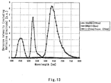
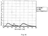
- An emission spectrum of light emitted from the organic electroluminescent device is controlled by varying a layer thickness of the metal doping layer.
- a light-emitting device having at least first and second light-emitting elements exhibiting different emission colors, each of the first and second light-emitting elements comprising:
- Example 1 describes a structure of a light-emitting element not being part of the present invention.
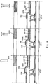
- a light-emitting element includes a first electrode 101 and a second electrode 102 that are opposed to each other, and a first layer 111, a second layer 112 and a third layer 113 are stacked in this order over the first electrode 101.
- holes are injected into the second layer 112 from the first layer 111 and electrons are injected into the second layer 112 from the third layer 113, when a voltage is applied to the light-emitting element such that a potential of the first electrode 101 are higher than that of the second electrode 102.
- the holes and electrons are recombined in the second layer 112 to excite a light-emitting substance.
- the excited light-emitting substance emits light when returning to the ground state.
- the thickness of at least one of the layers except the first electrode and the second electrode is made different in each of light-emitting elements exhibiting emission colors. Therefore, the light-extraction efficiency can be increased.
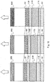
- light-emitting elements that emit light of red (R), green (G) and blue (B) share the first electrode 101 that has a non-light-transmitting property and the second electrode 102 that has a light-transmitting property, and further have first layers 111R, 111G and 111B, second layers 112R, 112G and 112B, and third layers 113R, 113G and 113B.
- the thicknesses of the first layers 111R, 111G and 111B are made different depending on each emission color.
- phase reversal is generated in the reflected light, thereby generating the effect of interference of light for reflected light and direct light.
- an optical distance between the light-emitting layer and the reflective electrode i.e., refractive index ⁇ distance
- ⁇ distance an optical distance between the light-emitting layer and the reflective electrode
- the light extraction efficiency is increased.
- the optical distance is m/2 times (m is a given positive integer), or, 1/2, 1, 3/2 ...-fold of the emission wavelength, the light-extraction efficiency is reduced.
- the thickness of at least one of the first to third layers is made different in each light-emitting element so that the optical distance between the light-emitting region and the reflective electrode, in other words, refractive index ⁇ distance, is (2m - 1)/4 fold (m is a given positive integer) of the emission wavelength.
- the thickness of a layer between the layer in which electrons and holes are recombined (i.e., light-emitting layer) and the reflective electrode may be made different, the thickness of the layer between the layer in which electrons and holes are recombined and a light-transmitting electrode may be made different. Alternatively, the thicknesses of the both layers may be made different. Consequently, light can be extracted outside efficiently.
- the same evaporation mask can be used.
- a photolithography process and an etching process are needed so as to make the thickness of an electrode different, and thus the number of processes is increased.
- any of the first to third layers is made different, a layer is needed to be thicker.
- a layer in which an organic compound and a metal oxide that is an inorganic compound are mixed is used as the layer to be made thicker.
- the driving voltage when the thickness of a layer in the light-emitting element becomes large, the driving voltage also increases, which is not preferable.
- the present inventors have found that the driving voltage itself can be lowered by using a layer in which an organic compound and a metal oxide that is an inorganic compound are mixed as the layer to be made thicker, without increasing the driving voltage.
- the thickness of at least one of the first to third layers is made different depending on each emission color.
- the thickness of a layer between a reflective electrode and a layer in which electrons and holes are recombined i.e., light-emitting layer
- it is preferable that a layer in which an organic compound and a metal oxide that is an inorganic compound are mixed is used as the layer to be made thicker, since a driving voltage does not become high.
- the Embodiment Mode describes a structure of a light-emitting element which is different from that of Example 1.
- a light-emitting element shown in this embodiment mode includes the first electrode 101 and the second electrode 102 that are opposed to each other, and the first layer 111, the second layer 112, the third layer 113 and a fourth layer 128 that are sequentially stacked over the first electrode 101.
- One feature of the light-emitting element is to have the fourth layer 128.
- the fourth layer 128 can be formed with the same material as that of the first layer 111.
- Other structures are the same as those of Embodiment Mode 1 and thus, the description thereof is omitted.
- the thickness of the fourth layer 128 is made different depending on each light-emitting element emitting each emission color. Consequently, the decrease of the light-extraction efficiency can be prevented.
- a metal oxide such as molybdenum oxide, vanadium oxide or rhenium oxide may be used as the fourth layer 128.
- a nitride or an oxynitride of these metals may be employed. This is because the driving voltage is not needed to be increased, even when the thickness is made larger using such metal oxides.
- Damages to underlayers in forming the second electrode 102 can be expected to be more reduced by making the fourth layer 128 thicker.
- the thickness of the first layer 111 can be made different depending on each light-emitting element emitting each emission color, as well as the fourth layer 128. Consequently, the thickness of the light-emitting element can be made more increased and defects in manufacturing can be reduced by making thicknesses of plural layers different, in addition to prevention of decrease in the light-extraction efficiency.
- the metal oxide described above such as molybdenum oxide, vanadium oxide or rhenium oxide, is used for the first layer 111, which does not increase the driving voltage.
- the present invention in which the thickness of a layer is made different depending on each light-emitting element emitting each emission color can be applied without limitations on a structure of a light-emitting element. As a result, decrease in the light-extraction efficiency can be prevented and the thickness of a light-emitting element can be increased. Further, the driving voltage is not made higher as the result of using a metal oxide or the like for the layer to be made thicker, which is preferable.
- Example 2 describes a structure in which the thickness of any of layers is made different in a light-emitting device including a color filter which is not part of the present invention.
- color filters 115R, 115G and 115B are provided in regions that are to exhibit red (R), green (G) and blue (B) that are different in optical characteristics, respectively.
- the color filters can be formed using a known material by a screen printing method, a droplet discharging method or the like.
- FIG. 16 shows the case where the color filters 105R, 105G and 105B are provided on the second electrode side 102 (on the emission side), and in this case, the second electrode 102 needs to be light-transmitting.
- the structure of the light-emitting element is as follows: the first layers 111R, 111G and 111B, the second layers 112R, 112G, and 112B, the third layers 113R, 113G and 113B, and the second electrode 102 are formed sequentially over the first electrode 101. Since each color is generated by the color filters, the first to third layers are formed using the same material. However, in FIG. 16 , the first to third layers are denoted by the first layers 111R, 111G and 111B, the second layers 112R, 112G, and 112B, the third layers 113R, 113G and 113B in order to correspond to each color filter.
- any of the first to third layers is made different depending on each color filter.
- the thickness of the second layers 112R, 112G and 112B is different depending on each color filter.
- phase reversal is generated in the reflected light, thereby generating the effect of interference of light for reflected light and direct light.
- an optical distance between the light-emitting layer and the reflective electrode i.e., refractive index ⁇ distance
- ⁇ distance an optical distance between the light-emitting layer and the reflective electrode
- the light extraction efficiency is increased.
- the optical distance is m/2 times (m is a given positive integer), or, 1/2, 1, 3/2 ...-fold of the emission wavelength, the light-extraction efficiency is reduced.
- the thickness of any of the first to third layers is made different depending on each color filter so that the optical distance between the layer in which electrons and holes are recombined (i.e., light-emitting layer) and the reflective electrode, in other words, refractive index ⁇ distance, is (2m - 1)/4 -fold (m is a given positive integer) of the emission wavelength.
- the thickness of a layer between the layer in which electrons and holes are recombined and the first electrode 101 serving as the reflective electrode may be made different.
- the thickness of a layer between the layer in which electrons and holes are recombined and the second electrode 102 serving as the light-transmitting electrode may be made different.
- the thicknesses of the both layers may be made different. Consequently, light can be extracted outside efficiently.
- the same evaporation mask can be used, which is preferable.
- a photolithography process and an etching process are needed to make the thickness of an electrode different, and thus the number of processes is increased.
- a layer is needed to be thicker because any of the first to third layers is made different.
- a layer in which an organic compound and a metal oxide that is an inorganic compound are mixed is used as the layer to be made thicker.
- the driving voltage when the thickness of a layer in the light-emitting element becomes large, the driving voltage also increases, which is not preferable.
- the present inventors have found that the driving voltage itself can be lowered by using a layer in which an organic compound and a metal oxide that is an inorganic compound are mixed is used as a layer to be made thicker, without increasing the driving voltage, even when the layer is made thicker.
- any of the first to third layers thicker, a short circuit between the first electrode 101 and second electrode 102 can be prevented, and productivity can be enhanced, which is preferable.
- FIG. 17 shows a case where color filters are provided on the first electrode side (on the emission side), which is different from that in FIG. 16 .
- Other structures are similar to those in FIG. 16 , and thus, the description thereof is omitted.
- the color filters are provided on the first electrode side as shown in FIG. 17 , a plurality of insulating films and the like constituting a part of a thin film transistor are stacked below the first electrode.
- the thickness of each layer is made different in consideration of light reflected by such insulating films and the like. Further, the insulating films and the like may be removed in a region through which light passes.
- the example as shown in FIG. 16 or 17 has one feature that the thickness of at least one of the first to third layers is made different depending on each color filter.
- the thickness of a layer between the layer in which electrons and holes are recombined (i.e., light-emitting layer) and the reflective electrode is preferably made different depending on each color filter.
- a layer in which an organic compound and a metal oxide that is an inorganic compound are mixed is used as the layer to be made thicker, since a driving voltage does not become high.
- Example 3 specifically describes a cross-sectional structure of a pixel including a color filter and a light-emitting element.
- a cross-sectional structure of a pixel in the case where a transistor for controlling current supplied to a light-emitting element (driving transistor) is a p-channel thin film transistor (TFT) is described with reference to FIG. 18 .
- TFT thin film transistor
- This example describes the case where the light-emitting element has two electrodes, namely, the first electrode 101 and the second electrode 102, and one of the first electrode 101 and the second electrode 102 whose potential can be controlled by a transistor is an anode and the other is a cathode.
- FIG. 18 is a cross-sectional view of a pixel including color filters 105R, 105G and 105B, in the case of a top emission type in which TFTs 601R, 601G and 601B are each p-channel type and light generated in a light-emitting element 603 is extracted through the second electrode 102.
- the first electrode 101 of the light-emitting element 603 is electrically connected to the TFTs 601R, 601G and 601B.
- the TFTs 601R, 601 G and 601B are 10 to 200 nm thick, and their channel forming regions are formed with island-like semiconductor films. Any of an amorphous semiconductor film, a crystalline semiconductor film, and a microcrystalline semiconductor film may be used as the semiconductor film.
- the amorphous semiconductor film is formed first and is heated to be crystallized by a heat treatment to form a crystalline semiconductor film.
- the heat treatment can be conducted using a heating furnace, laser irradiation, light-irradiation from a lamp instead of laser light (hereinafter, lamp annealing), or a combination thereof.
- CW laser continuous wave
- pulsed laser a continuous wave (CW) laser or a pulsed laser may be used.
- the laser irradiation may be conducted so that the incident angle ⁇ of laser light with respect to a semiconductor film is 0° ⁇ ⁇ ⁇ 90°. Consequently, an interference of laser light can be prevented.
- the semiconductor film may be irradiated with continuous wave laser light of a fundamental wave and continuous wave laser light of a harmonic, or may be irradiated with continuous wave laser light of a fundamental wave and pulsed wave laser light of a harmonic. Energy can be supplemented by irradiating with plural kinds of laser light.
- a pulsed laser may be oscillated with such a repetition rate that the laser of the next pulse is emitted before solidifying the semiconductor film that has been melted. This makes it possible to obtain crystal grains which are sequentially grown in the scanning direction.
- a pulsed beam with a lower limit of a repetition rate that is set shorter than the time required for the melted semiconductor film to solidify.
- the pulsed beam that can be used actually is a repetition rate of 10 MHz or more. This repetition rate is extremely higher than that of the pulsed laser used usually, which is from several tens to several hundred Hz, to conduct laser crystallization.
- an amorphous semiconductor film is heated at a temperature of 500 to 550 °C for 2 to 20 hours.
- the temperature may be set in multiple stages in the range of 500 to 550 °C so as to gradually reach a higher temperature. This is because so-called dehydrogenation can be performed to reduce film roughness during crystallization, since hydrogen and the like of the amorphous semiconductor film are released in the first low temperature heating process.
- a metal element for promoting crystallization for example, Ni
- the heat temperature can be lowered, which is preferable. Even in the case of crystallization using such a metal element, a heat treatment may be performed at a temperature of 600 to 950 °C.
- a gettering process is required to reduce or remove the metal element.
- a process of gettering the metal element may be performed using the amorphous semiconductor film as a gettering sink.
- a gate insulating film covering the semiconductor film, a gate electrode in which a fist conductive film and a second conductive film are stacked, an insulating film over the gate electrode are provided.
- the TFTs 601R, 601G and 601B are each p-channel type, and the semiconductor film has a single drain structure having only a high concentration impurity region.
- the TFTs 601R, 601G and 601B may have an LDD (lightly doped drain) structure in which a low concentration impurity region and a high concentration impurity region are provided in the semiconductor film.
- the TFTs 601R, 601G and 601B are covered with an interlayer insulating film 607, and a bank 608 having an opening portion is formed over the interlayer insulating film 607.
- the first electrode 101 is partially exposed in the opening portion of the bank 608, and the first electrode 101, electroluminescent layers 605R, 605G and 605B, and the second electrode 102 are sequentially stacked in the opening portion.
- the electroluminescent layers can be formed using the same material; however, the electroluminescent layers are denoted by the electroluminescent layers 605R, 605G and 605B so as to correspond to each color filter in the drawing.
- the electroluminescent layers 605R, 605G and 605B correspond to the first to third layers 111, 112 and 113, and the thickness of any of the first to third layers is made different depending on each color filter.
- the relationship between the thicknesses of the electroluminescent layers becomes 605R ⁇ 605G ⁇ 605B.
- This example shows a top emission type, and thus, the thickness of the first layers closest to the first electrode 101 may be different depending on each color filter. As a result, decrease in the light-extraction efficiency can be prevented.
- increase in driving voltage due to a thicker thickness can be prevented by using a layer in which an organic compound and a metal oxide are mixed as the first layer.
- the first electrode 101 is formed using a non-light-transmitting material, in other words, highly reflective material.
- the concrete materials thereof are shown in examples described above.
- the second electrode 102 is preferably formed using a light-transmitting material, more preferably, a substance having a high work function.
- a light-transmitting material more preferably, a substance having a high work function.
- the concrete materials thereof are shown in examples described above.
- the transistor for controlling supply is p-channel type
- a wiring connected to the TFTs 601 R, 601 G and 601 B can be used as the first electrode 101.
- the first electrode 101 or the second electrode 102 can be formed by a sputtering method, an evaporation method or the like.
- the interlayer insulating film 607 is formed using an organic resin material, an inorganic insulating material, or an insulator including Si-O-Si bond, which is formed from a siloxane based material.
- Siloxane based insulator has a skeleton formed by the bond of silicon (Si) and oxygen (O), in which a compound containing at least hydrogen (such as an alkyl group or aromatic hydrocarbon) is included as a substituent.
- a fluoro group may be used as a substituent.
- a compound containing at least hydrogen and a fluoro group may be used as a substituent.
- a material referred to as a low dielectric constant material (low-k material) may be used for the interlayer insulating film 607.
- the bank 608 can be formed using an organic resin material, an inorganic insulating material or a siloxane based insulator.
- an organic resin material acrylic, polyimide, polyamide and the like can be used as the organic resin material
- silicon oxide, silicon nitride oxide and the like can be used as the inorganic insulating material.
- a photosensitive organic resin material is used for the bank 608, an opening portion is formed over the first electrode 101 so that the side of the opening portion has an inclined plane with a continuous curvature. As a result, a short circuit between the first electrode 101 and the second electrode 102 can be prevented.
- FIG 19 is a cross-sectional view of a pixel in the case of a bottom emission type in which TFTs 601R, 601 G and 601B are each p-channel type and light generated in a light-emitting element 603 is extracted through the second electrode 102.
- the first electrode 101 of the light-emitting element 603 is electrically connected to the TFTs 601R, 601G and 601B.
- electroluminescent layers 605R, 605G and 605B, and the second electrode 102 are sequentially stacked over the first electrode 101.
- the TFTs 601R, 601G and 601B can be formed in the same manner as in FIG 18 .
- the first electrode 101 has a light-transmitting property and the second electrode 102 has a non-light-transmitting property.
- Materials of the electrodes can be referred to the description of the first electrode and the second electrode in FIG. 18 .
- Color filters 105R, 105G and 105B are provided on the substrate side (on the emission side).
- the color filters 105R, 105G and 105B can be provided for a rear face of the substrate (i.e., a surface in which TFTs are not formed).
- the electroluminescent layers 605R, 605G and 605B can be formed in the same manner as the electroluminescent layers shown in FIG 18 , and the thickness of at least one of the first to third layers is different depending on each color filter. Since the bottom emission type is shown in FIG. 19 , the thickness of the third layer closest to the second electrode 102 may be made different depending on each color filter. In this example, the relationship between the thicknesses of the electroluminescent layers is 605R ⁇ 605G ⁇ 605B. Consequently, decrease in the light-extraction efficiency can be prevented.
- a layer in which an organic compound and a metal oxide are mixed is used as the third layer, thereby preventing the increase of the driving voltage due to the thicker thickness.
- light emitted from the light-emitting element 613 can be extracted through the second electrode 102 as shown by the outline arrow, and the color filters 105R, 105G and 105B are provided on the emission side.
- Example 4 specifically describes a cross-sectional structure of a pixel having a color filter and a light-emitting element, in the case where a transistor for controlling current supplied to a light-emitting element (driving transistor) is an n-channel thin film transistor (TFT).
- driving transistor n-channel thin film transistor
- TFT thin film transistor
- FIG 20 is a cross-sectional view of a pixel in the case of a top emission type in which TFTs 611 R, 611 G and 611 B are each n-channel type and light generated in a light-emitting element 613 is extracted through the second electrode 102.
- the first electrode 101 of the light-emitting element 613 is electrically connected to the TFTs 611R, 611G and 611B.
- electroluminescent layers 615R, 615G and 615B, and the second electrode 102 are sequentially stacked over the first electrode 101.
- the TFTs 611 R, 611 G and 611 B can be formed in the same manner as TFTs 601R, 601G and 601B in the example described above.
- the first electrode 101 is formed using a non-light-transmitting material and the second electrode 102 is formed using a light-transmitting material.
- the materials can be referred to the examples described above.
- the transistor for controlling supply is n-channel type, a wiring connected to the TFTs 611R, 611G and 611 B can be used as the first electrode 101.
- the color filters 105R, 105G and 105B are provided on the second electrode 102 side.
- the second electrode has a light-transmitting property.
- the electroluminescent layers 615R, 615G and 615B can be formed in the same manner as the electroluminescent layers 605R, 605G and 605B in the example described above.
- the hole injecting layer, the hole transporting layer, the light-emitting layer, the electron transporting layer and the electron injecting layer are stacked in this order on the first electrode 101, since the first electrode 101 is an anode, when the electroluminescent layer 615 has, in addition to the light-emitting layer, any of the following: the hole injecting layer, the hole transporting layer, the electron transporting layer and the electron injecting layer.
- the electroluminescent layers 615R, 615G and 615B correspond to the first to third layers 111, 112 and 113, and the thickness of any of the first to third layers is made different depending on each color filter. Since the top emission type is shown in this example, the thickness of the first layer closest to the first electrode 101 may be made different depending on each color filter. In this example, the relationship between the thicknesses of the electroluminescent layers is 615R ⁇ 615G ⁇ 615B. Consequently, decrease in the light-extraction efficiency can be prevented.
- a layer in which an organic compound and a metal oxide are mixed is used as the first layer, thereby preventing the increase of the driving voltage due to the thicker thickness.
- light emitted from the light-emitting element 613 can be extracted through the second electrode 102 as shown by the outline arrow, and the color filters 105R, 105G and 105B are provided on the emission side.
- FIG. 21 is a cross-sectional view of a pixel having each emission color (RGB), in the case of a bottom emission type in which TFTs 611R, 611G and 611B are each n-channel type and light generated in a light-emitting element 613 is extracted through the first electrode 101.
- RGB emission color
- the first electrode 101 of the light-emitting element 613 is electrically connected to the TFTs 611R, 611G and 611B.
- electroluminescent layers 615R, 615G and 615B, and the second electrode 102 are sequentially stacked over the first electrode 101.
- the TFTs 611 R, 611 G and 611 B can be formed in the same manner as in the example described above.
- the first electrode 101 has a light-transmitting property and the second electrode 102 has a non-light-transmitting property.
- the materials thereof can be referred to the examples described above.
- the color filters 105R, 105G and 105B are provided on the first electrode 101 side.
- the first electrode 101 has a light-transmitting property.
- the electroluminescent layers 615R, 615G and 615B can also be formed in the same manner as in the examples described above and the thickness of any of the first to third layers is made different depending on each color filter.
- the hole injecting layer, the hole transporting layer, the light-emitting layer, the electron transporting layer and the electron injecting layer are stacked in this order on the first electrode 101, since the first electrode 101 is an anode, when the electroluminescent layer 615 has, in addition to the light-emitting layer, any of the following: the hole injecting layer, the hole transporting layer, the electron transporting layer and the electron injecting layer.
- the thickness of the third layer closest to the second electrode 102 is made different depending on each color filter.
- the relationship between the thicknesses of the electroluminescent layers is 615R ⁇ 615G ⁇ 615B. Consequently, decrease in the light-extraction efficiency can be prevented.
- a layer in which an organic compound and a metal oxide are mixed is used as the third layer, thereby preventing the increase of the driving voltage due to the thicker thickness.
- light emitted from the light-emitting element 613 can be extracted through the first electrode 101 as shown by the outline arrow, and the color filters 105R, 105G and 105B are provided on the emission side.
- the first layer 111 is a layer generating holes.
- a layer containing a substance having hole transporting property and a substance having electron accepting property with respect to the substance having hole transporting property (in other words, the substance serving as an acceptor for the substance having hole transporting property) can be given.
- the substance having electron accepting property with respect to the substance having hole transporting property is preferably included so as to satisfy a molar ratio (i.e., the substance having electron accepting property with respect to the substance having hole transporting property/the substance having hole transporting property) of 0.5 to 2.
- the substance having hole transporting property indicates a substance having a strong property of transporting holes rather than electrons.
- An organic compound for example, an aromatic amine compound such as 4, 4'-bis[N-(1-naphthyl)-N-phenylamino]biphenyl ( ⁇ -NPD), 4,4'-bis[N-(3-methylphenyl)-N-phenylamino]biphenyl (TPD), 4,4',4"-tris(N,N-diphenylamino)triphenylamine (TDATA), 4,4',4"-tris[N-(3-methylphenyl)-N-phenylamino]triphenylamine (MTDATA), and 4,4'-bis ⁇ N-[4-(N,N-di-m-tolylamino)phenyl]-N-phenylamino ⁇ biphenyl (DNTPD); a phthalocyanine compound such as phthalocyanine (H 2 Pc), copper phthal
- a carbazole derivative such as 4,4'-di(N-carbazolyl)biphenyl (CBP) or an aromatic hydrocarbon compound such as 9,10-di(2-naphthyl)-2-tert-butylanthracene (t-BuDNA) can be applied.
- CBP 4,4'-di(N-carbazolyl)biphenyl
- t-BuDNA 9,10-di(2-naphthyl)-2-tert-butylanthracene
- a metal oxide such as molybdenum oxide, vanadium oxide, or ruthenium oxide can be used. Further, a nitride or an oxynitride of the metals may be employed.
- the substance having electron accepting property with respect to the substance having hole transporting property is not limited thereto.
- the first layer 111 in which the substance having hole transporting property and the substance having electron accepting property with respect to the substance having hole transporting property are mixed can be formed by a co-evaporation method.
- the first layer 111 can be formed by combining the same methods or different methods, for example, a co-evaporation method using resistance heating evaporation, a co-evaporation method using electron beam evaporation, a co-evaporation method using resistance heating evaporation and electron beam evaporation, a formation method using resistance heating evaporation and sputtering, a formation method using electron beam evaporation and sputtering, and the like.
- the above described examples are given in consideration of forming a layer including two types of materials; however, a layer including three or more types of materials can also be formed by combining the same methods or different methods as well.
- the first layer 111 may include another organic compound, for example, rubrene. Reliability can be enhanced by adding rubrene.
- the first layer 111 may be a layer including a metal oxide such as molybdenum oxide, vanadium oxide, ruthenium oxide, cobalt oxide or copper oxide.
- a nitride or an oxynitride of the metals may be employed.
- the first layer 111 is formed with the layer containing an organic compound and a metal oxide as described above, since the conductivity can be enhanced at this time.
- the conductivity is high, the first layer 111 can be made thicker.
- the second layer 112 is a layer including a light-emitting layer.
- the second layer 112 may have a single layer structure or a multilayer structure.
- the second layer 112 may have a multilayer structure including a hole transporting layer 121, an electron transporting layer 123, and an electron injecting layer 124, in addition to the light-emitting layer 122, or a single layer of the light-emitting layer 122.
- the light-emitting substance is a substance that has a favorable light-emitting efficiency and can emit light of a desired emission wavelength.
- the second layer 112 is preferably formed using a layer in which a light-emitting substance is dispersed in a layer of a substance having a larger energy gap than that of the light-emitting substance.
- the second layer is not limited thereto.
- the energy gap indicates an energy gap between the LUMO level and the HOMO level.
- the light-emitting substance may be a substance that has a favorable light-emitting efficiency and can emit light of a desired emission wavelength.
- an anthracene derivative such as 9,10-di(2-naphthyl)-2-tert-butylanthracene (t-BuDNA); a carbazole derivative such as 4,4'-di(N-carbazolyl)biphenyl (CBP); a metal complex such as bis[2-(2-hydroxyphenyl)pyridinato]zinc (Znpp 2 ) and bis[2-(2-hydroxyphenyl)benzoxazolato]zinc (ZnBOX); and the like can be used.
- the substance used for dispersing a light-emitting substance is not particularly limited to these materials. Note that quenching of light emitted from the light-emitting substance due to the concentration of the light-emitting substance can be prevented by employing the structure.
- the following substances can be employed: 4-dicyanomethylene-2-isopropyl-6-[2-(1,1,7,7-tetramethyljulolidine-9-yl)ethenyl]-4H-p yran (DCJTI); 4-dicyanomethylene-2-methyl-6-[2-(1,1,7,7-tetramethyljulolidine-9-yl)ethenyl]-4H-pyr an (DCJT); 4-dicyanomethylene-2-tert-butyl-6-[2-(1,1,7,7-tetramethyljulolidine-9-yl)ethenyl]-4H-p yran (DCJTB); periflanthene; 2,5-dicyano-1,4-bis[2-(10-methoxy-1,1,7,7-tetramethyljulolidine-9-yl)ethenyl]benzene; bis[2,3 - bis(4 - fluorophenyl
- substances such as N,N'-dimethylquinacridon (DMQd), coumarin 6, coumarin 545T, and tris(8-quinolinolate)aluminum (Alq 3 ) can be employed.
- DMQd N,N'-dimethylquinacridon
- coumarin 6, coumarin 545T and tris(8-quinolinolate)aluminum (Alq 3 )
- Alq 3 tris(8-quinolinolate)aluminum
- the present invention is not limited to these materials, and a substance that can emit light with a peak of emission spectrum in 500 to 550 nm can be used.
- the following substances can be employed: 9,10-bis(2-naphthyl)-tert-butylanthracene (t-BuDNA); 9,9'-bianthryl; 9,10-diphenylanthracene (DPA); 9,10-bis(2-naphthyl)anthracene (DNA); bis(2-methyl-8-quinolinolate)-4-phenylphenolate-gallium (BGaq); bis(2-methyl-8-quinolinolate)-4-phenylphenolate-aluminum (BAlq); and the like.
- the present invention is not limited to these materials, and a substance that can emit light with a peak of emission spectrum in 420 to500 nm can be used.
- the third layer 113 is a layer generating electrons.
- a layer including a substance having electron transporting property and a substance having electron donating property with respect to the substance having electron transporting property can be given.
- the substance having electron transporting property is a substance having a strong property of transporting electrons rather than holes.
- a metal complex such as tris(8-quinolinolato)aluminum (Alq 3 ), tris(4-methyl-8-quinolinolato)aluminum (Almq 3 ), bis(10-hydroxybenzo[h]-quinolinato)beryllium (BeBq 2 ), bis(2-methyl-8-quinolinolato)-4-phenylphenolate-aluminum (BAlq), bis[2-(2-hydroxyphenyl)benzoxazolate]zinc (Zn(BOX) 2 ), bis[2-(2-hydroxyphenyl)benzothiazolate]zinc (Zn(BTZ) 2 ) can be used.
- Alq 3 tris(8-quinolinolato)aluminum
- Almq 3 tris(4-methyl-8-quinolinolato)aluminum
- BeBq 2 bis(2-methyl-8-quinolinolato)-4-phenylphenolate-aluminum
- BAlq
- the following substances can be used as the substance having electron transporting property: 2-(4-biphenylyl)-5-(4-tert-butylphenyl)-1,3,4-oxadiazole (PBD); 1,3-bis[5-(p-tert-butylphenyl)-1,3,4-oxadiazole-2-yl]benzene (OXD-7); 3-(4-tert-butylphenyl)-4-phenyl-5-(4-biphenylyl)-1,2,4-triazole (TAZ); 3-(4-tert-butylphenyl)-4-(4-ethylphenyl)-5-(4-biphenylyl)-1,2,4-triazole (p-EtTAZ); bathophenanthroline (BPhen); bathocuproin (BCP); 4,4'-bis(5-methylbenzoxazolyl-2-yl)stilbene (BzOs) and the like.
- an alkali metal such as lithium and cesium, alkaline earth metal such as magnesium and calcium, rare-earth metal such as erbium and ytterbium, and the like can be used as the substance having electron donating property with respect to the substance having electron transporting property.
- the substance having electron donating property with respect to the substance having electron transporting property is not limited thereto.
- the third layer 113 includes the substance having electron donating property with respect to the substance having electron transporting property and the substance having electron transporting property so as to satisfy a molar ratio (i.e., the substance having electron donating property with respect to the substance having electron transporting property / the substance having electron transporting property) of 0.5 to 2.
- the third layer 113 may include a substance such as zinc oxide, zinc sulfide, zinc selenide, tin oxide and titanium oxide.
- the difference in electron affinity between the substance having electron transporting property, which is included in the third layer 113 and a substance, which is included in a layer in contact with the third layer 113 among the layers included in the second layer 112, is preferably set to be 2 eV or less, more preferably, 1.5 eV or less.
- the difference between a work function of the n-type semiconductor and the electron affinity of the substance, which is included in the layer in contact with the third layer 113 among the layers included in the second layer 112 is preferably 2 eV or less, more preferably, 1.5 eV or less.
- the layer in contact with the third layer 113 among the layers included in the second layer 112 corresponds to the electron injecting layer 124 in the case where the second layer 112 has a stacked structure.
- the second layer 112 may have a single layer structure of a light-emitting layer or a structure without the electron injecting layer 124 or the like.
- the second layer 112 and the second electrode 102 are joined by the third layer 113, and thus, electrons can be easily injected from the second electrode 102 into the second layer 112.
- One of the first electrode 101 and the second electrode 102 can transmit visible light and is formed using a conductive substance. Therefore, light can be extracted outside through one of the first electrode 101 and the second electrode 102 described above.
- the first electrode 101 in addition to aluminum (Al) or a light-transmitting material such as indium tin oxide (ITO), indium tin oxide containing silicon oxide (hereinafter, also referred to as ITSO), or indium oxide containing zinc oxide of 2 to 20 %, a metal material such as gold (Au), platinum (Pt), nickel (Ni), tungsten (W), chromium (Cr), molybdenum (Mo), iron (Fe), cobalt (Co), copper (Cu) or palladium (Pd), or a stacked structure of the metals can be used.
- a metal material such as gold (Au), platinum (Pt), nickel (Ni), tungsten (W), chromium (Cr), molybdenum (Mo), iron (Fe), cobalt (Co), copper (Cu) or palladium (Pd), or a stacked structure of the metals can be used.
- the metal material is made thin to become semi-transparent and a transparent material is stacked thereover.
- a single layer of a semi-transparent metal material may be used.
- the materials of the first electrode are not limited to these materials.
- the second electrode 102 in addition to a light-transmitting material such as indium tin oxide (ITO), indium tin oxide containing silicon oxide (ITSO), or indium oxide containing zinc oxide of 2 to 20 %, a metal material such as gold (Au), platinum (Pt), nickel (Ni), tungsten (W), chromium (Cr), molybdenum (Mo), iron (Fe), cobalt (Co), copper (Cu) or palladium (Pd), or a stacked structure of the metals can be used.
- the metal material is made thin to become semi-transparent, and a transparent material is stacked thereover.
- a single layer of a semi-transparent metal material may be used.
- the materials of the second electrode are not limited to these materials.
- the first electrode 101 or the second electrode 102 can be formed by a sputtering method, an evaporation method or the like.
- the electron transporting layer 123 can be formed between the third layer 113 and the light-emitting layer 122. In this manner, the distance from the light-emitting layer 122 to the second electrode 102 or the third layer 113 can be increased by providing the electron transporting layer 123. Thus, quenching of light due to the metal can be prevented.
- the electron transporting layer 123 has a function of transporting injected electrons to the light-emitting layer 122.
- the electron transporting layer 123 can be formed using the above-described Alq 3 , Almq 3 , BeBq 2 , BAlq, Zn(BOX) 2 , Zn(BTZ) 2 , PBD, OXD-7, TAZ, p-EtTAZ, BPhen, BCP, or the like. Without being limited to these materials, the electron transporting layer 123 may be formed by using an substance having electron transporting property in which the electron mobility is higher than the hole mobility. Also, the electron transporting layer 123 is preferably formed by using a substance having the electron mobility of 10 -6 cm 2 /Vs or more. Further, the electron transporting layer 123 may have a multilayer structure formed by stacking two or more layers made from the above-described substances.
- the electron injecting layer 124 may be provided between the second electrode 102 and the electron transporting layer 123.
- the electron injecting layer 124 has a function of helping the injection of holes into the electron transporting layer 123 from the second electrode 102.
- the electron injecting layer 124 is not necessarily provided. In other words, the third layer 113 can also have a function of helping electrons to be injected.
- the hole transporting layer 121 is provided between the first electrode 101 and the light-emitting layer 122 as described above. By providing the hole transporting layer 121, the distance from the light-emitting layer 122 to the first electrode 101 or the first layer 111 can be increased, and thus, quenching of light generated in the light-emitting layer due to the metal can be prevented. Note that the hole transporting layer 121 is a layer having a function of transporting holes injected from the first electrode 101 to the light-emitting layer 122.
- the above-described ⁇ -NPD, TPD, TDATA, MTDATA, DNTPD and the like can be used for the hole transporting layer 121.
- the hole transporting layer 121 is not particularly limited thereto.
- the hole transporting layer 121 can be formed using the above-described substance with a hole transporting property of which the hole mobility is higher than the electron mobility.
- the hole transporting layer 121 is preferably formed using a substance having the hole mobility of 10 -6 cm 2 /Vs or more.
- the hole transporting layer 121 may have a multilayer structure formed by stacking two or more layers including the above-described substances.
- the hole transporting layer 121 can be formed using a metal oxide such as molybdenum oxide, vanadium oxide, ruthenium oxide, tungsten oxide or manganese oxide.
- the hole transporting layer 121 can be formed using the above-described phthalocyanine based compound such as H 2 Pc, CuPC and VOPc, the aromatic amine compound such as DNTPD, or a high molecular weight material such as a poly(ethylenedioxythiophene)/poly(styrene sulfonate) mixture (PEDOT/PSS).
- the hole transporting layer 121 may be formed using the above-described layer including the substance with the hole transporting property and the substance having the electron accepting property with respect to the substance with the hole transporting property.
- the hole transporting layer 121 is not limited to these.
- the hole transporting layer 121 can also be served as the first layer 111.
- Example 5 specifically describes a cross-sectional structure of a pixel included in a light-emitting element.
- a cross-sectional structure of a pixel in the case where a transistor for controlling current supplied to a light-emitting element (driving transistor) is a p-channel thin film transistor (TFT) is described using FIG. 3 .
- driving transistor a transistor for controlling current supplied to a light-emitting element
- TFT p-channel thin film transistor
- FIG. 3 is a cross-sectional view of a pixel having RGB, in the case of a top emission type in which TFTs 601R, 601G and 601 B are each p-channel type and light generated in a light-emitting element 603 is extracted through the second electrode 102.
- the first electrode 101 of the light-emitting element 603 is electrically connected to the TFTs 601R, 601G and 601B.
- the TFTs 601R, 601G and 601 B are 10 to 200 nm thick, and channel forming regions are formed with island-like semiconductor films. Any of an amorphous semiconductor film, a crystalline semiconductor film, and a microcrystalline semiconductor film may be used as the semiconductor film as in the above-described example.
- the amorphous semiconductor film is formed first and is heated to be crystallized by a heat treatment to form a crystalline semiconductor film.
- the heat treatment can be conducted by a heating furnace, laser irradiation, lamp annealing, or a combination thereof.
- CW continuous wave
- pulsed laser In the case of laser irradiation, a continuous wave (CW) laser or a pulsed laser can be used.
- Laser irradiation may be conducted so that the incident angle ⁇ of laser light with respect to a semiconductor film is 0° ⁇ ⁇ ⁇ 90°. Consequently, an interference of laser light can be prevented.
- the semiconductor film may be irradiated with continuous wave laser light of a fundamental wave and continuous wave laser light of a harmonic, or may be irradiated with continuous wave laser light of a fundamental wave and pulsed wave laser light of a harmonic. Energy can be supplemented by irradiating with plural kinds of laser light.
- a pulsed laser may be oscillated with such a repetition rate that the laser of the next pulse is emitted before solidifying the semiconductor film that has been melted. This makes it possible to obtain crystal grains which are sequentially grown in the scanning direction.
- a pulsed beam with a lower limit of a repetition rate that is set shorter than the time required for the melted semiconductor film to solidify.
- the pulsed beam that can be used actually is a repetition rate of 10 MHz or more. This repetition rate is extremely higher than that of the pulsed laser used usually, which is from several tens to several hundred Hz, to conduct laser crystallization.
- an amorphous semiconductor film is heated at a temperature of 500 to 550 °C for 2 to 20 hours.
- the temperature may be set in multiple stages in the range of 500 to 550 °C so as to gradually reach a higher temperature. This is because so-called dehydrogenation can be performed to reduce film roughness during crystallization, since hydrogen and the like of the amorphous semiconductor film are released in the first low temperature heating process.
- a metal element for promoting crystallization for example, Ni
- the heat temperature can be lowered, which is preferable. Even in the case of crystallization using such a metal element, a heat treatment may be performed at a temperature of 600 to 950 °C.
- a gettering process is required to reduce or remove the metal element.
- a process of gettering the metal element may be performed using the amorphous semiconductor film as a gettering sink.
- a gate insulating film covering the semiconductor film, a gate electrode in which a fist conductive film and a second conductive film are stacked, an insulating film over the gate electrode are provided.
- the TFTs 601R, 601 G and 601 B are each p-channel type, and the semiconductor film has a single drain structure having only a high concentration impurity region.
- the TFTs 601R, 601G and 601B may have an LDD (lightly doped drain) structure in which a low concentration impurity region and a high concentration impurity region are provided in the semiconductor film.
- the TFTs 601R, 601G and 601 B are covered with an interlayer insulating film 607, and a bank 608 having an opening portion is formed over the interlayer insulating film 607.
- the first electrode 101 is partially exposed in the opening portion of the bank 608, and the first electrode 101, electroluminescent layers 605R, 605G and 605B, and the second electrode 102 are sequentially stacked in the opening portion.
- the electroluminescent layers 605R, 605G and 605B correspond to the first to third layers 111, 112 and 113, and the thickness of any of the first to third layers is made different depending on each emission color.
- This example shows a top emission type, and thus, the thickness of the first layers closest to the first electrode 101 may be different depending on each emission color. As a result, decrease in the light-extraction efficiency can be prevented.
- increase in driving voltage due to a thicker thickness can be prevented by using a layer in which an organic compound and a metal oxide are mixed as the first layer.
- the thickness of the third layer can also be made different depending on each emission color.
- the first electrode 101 is formed using a non-light-transmitting material, in other words, highly reflective material.
- metal materials such as aluminum (Al), gold (Au), platinum (Pt), nickel (Ni), tungsten (W), chromium (Cr), molybdenum (Mo), iron (Fe), cobalt (Co), copper (Cu) and palladium (Pd) can be given.
- a stacked structure of light-transmitting materials such as indium tin oxide (ITO), indium tin oxide containing silicon oxide (ITSO), and indium oxide containing zinc oxide of 2 to 20 % may be used.
- the material of the first electrode is not limited thereto.
- the second electrode 102 is formed using a light-transmitting material and preferably, a substance having a high work function. Specifically, indium tin oxide (ITO), indium tin oxide containing silicon oxide (ITSO), and indium oxide containing zinc oxide of 2 to 20 % can be used. In addition, gold (Au), platinum (Pt), nickel (Ni), tungsten (W), chrome (Cr), molybdenum (Mo), iron (Fe), cobalt (Co), copper (Cu), palladium (Pd) or the like, each of which is not light-transmitting, can be used by making them thin enough to transmit light. A stacked structure of these materials can also be used. However, the material of the second electrode is not limited thereto.
- the transistor for controlling supply is p-channel type
- a wiring connected to the TFTs 601R, 601G and 601 B can be used as the first electrode 101.
- the first electrode 101 or the second electrode 102 can be formed by a sputtering method, an evaporation method or the like.
- the interlayer insulating film 607 is formed using an organic resin material, or an inorganic insulating material, or a siloxane based insulator. Moreover, a material referred to as a low dielectric constant material (low-k material) may be used for the interlayer insulating film 607.
- a low dielectric constant material low-k material
- the bank 608 can be formed using an organic resin material, an inorganic insulating material or a siloxane based insulator.
- an organic resin material acrylic, polyimide, polyamide and the like can be used as the organic resin material
- silicon oxide, silicon nitride oxide and the like can be used as the inorganic insulating material.
- a photosensitive organic resin material is used for the bank 608, an opening portion is formed over the first electrode 101 so that the side of the opening portion has an inclined plane with a continuous curvature. As a result, a short circuit between the first electrode 101 and the second electrode 102 can be prevented.
- FIG 4 is a cross-sectional view of a pixel having each emission color (RGB) in the case of a bottom emission type in which TFTs 601R, 601G and 601B are each p-channel type and light generated in a light-emitting element 603 is extracted through the second electrode 102.
- RGB emission color
- the first electrode 101 of the light-emitting element 603 is electrically connected to the TFTs 601R, 601G and 601B.
- electroluminescent layers 605R, 605G and 605B, and the second electrode 102 are sequentially stacked on the first electrode 101.
- the TFTs 601R, 601G and 601 B can be formed in the same manner as in FIG. 3 .
- the first electrode 101 has a light-transmitting property and the second electrode 102 has a non-light-transmitting property. Materials of the electrodes can be referred to the description of the first electrode and the second electrode in FIG. 3 .
- the electroluminescent layers 605R, 605G and 605B can be formed in the same manner as the electroluminescent layers shown in FIG 3 , and the thickness of any of the first to third layers is different depending on each of R, G and B. Since the bottom emission type is shown in FIG. 4 , the thickness of the third layer closest to the second electrode 102 may be made different depending on each emission color. Consequently, decrease in the light-extraction efficiency can be prevented.
- a layer in which an organic compound and a metal oxide are mixed is used as the third layer, thereby preventing the increase of the driving voltage due to the thicker thickness. Note that the thickness of the first layer can be made different depending on each emission color.
- light emitted from the light-emitting element 613 can be extracted through the second electrode 102 as shown by the outline arrow.
- Example 6 not being part of the present invention, specifically describes a cross-sectional structure of a pixel in the case where a transistor for controlling current supplied to a light-emitting element (driving transistor) is an n-channel thin film transistor (TFT).
- driving transistor n-channel thin film transistor
- TFT thin film transistor
- FIG 5 is a cross-sectional view of a pixel in the case of a top emission type in which TFTs 611R, 611G and 611 B are each n-channel type and light generated in a light-emitting element 613 is extracted through the second electrode 102.
- the first electrode 101 of the light-emitting element 613 is electrically connected to the TFTs 611R, 611G and 611B.
- electroluminescent layers 615R, 615G and 615B, and the second electrode 102 are sequentially stacked on the first electrode 101.
- the TFTs 611R, 611G and 611B can be formed in the same manner as TFTs 601 R, 601 G and 601 B in the example described above.
- the first electrode 101 is formed using a non-light-transmitting material and the second electrode 102 is formed using a light-transmitting material.
- the materials of the electrodes can be referred to the examples described above.
- the transistor for controlling supply of current is n-channel type, a wiring connected to the TFTs 611R, 611G and 611B can be used as the first electrode 101.
- the electroluminescent layers 615R, 615G and 615B can be formed in the same manner as the electroluminescent layers 605R, 605G and 605B in the example described above.
- the hole injecting layer, the hole transporting layer, the light-emitting layer, the electron transporting layer and the electron injecting layer are stacked in this order on the first electrode 101, since the first electrode 101 is an anode, when the electroluminescent layer 615 has, in addition to the light-emitting layer, any of the following: the hole injecting layer, the hole transporting layer, the electron transporting layer and the electron injecting layer.
- the electroluminescent layers 615R, 615G and 615B correspond to the first to third layers 111, 112 and 113, and the thickness of any of the first to third layers is made different depending on each emission color. Since the top emission type is shown in this example, the thickness of the first layer closest to the first electrode 101 is made different depending on each emission color. Consequently, decrease in the light-extraction efficiency can be prevented.
- a layer in which an organic compound and a metal oxide are mixed is used as the first layer, thereby preventing the increase of the driving voltage due to the thicker thickness. Note that the thickness of the third layer can be made different depending on each emission color.
- light emitted from the light-emitting element 613 can be extracted through the second electrode 102 as shown by the outline arrow.
- FIG 6 is a cross-sectional view of a pixel having each emission color (RGB), in the case of a bottom emission type in which TFTs 611R, 611G and 611 B are each n-channel type and light generated in a light-emitting element 613 is extracted through the first electrode 101.
- RGB emission color
- the first electrode 101 of the light-emitting element 613 is electrically connected to the TFTs 611R, 611G and 611B.
- electroluminescent layers 615R, 615G and 615B, and the second electrode 102 are sequentially stacked on the first electrode 101.
- the TFTs 611 R, 611G and 611 B can be formed in the same manner as in the example described above.
- the first electrode 101 has a light-transmitting property and the second electrode 102 has a non-light-transmitting property.
- the materials thereof can be referred to the examples described above.
- the electroluminescent layers 615R, 615G and 615B can also be formed in the same manner as in the examples described above and the thickness of any of the first to third layers is made different depending on each of R, G and B.
- the hole injecting layer, the hole transporting layer, the light-emitting layer, the electron transporting layer and the electron injecting layer are stacked in this order on the first electrode 101, since the first electrode 101 is an anode, when the electroluminescent layer 615 has, in addition to the light-emitting layer, any of the following: the hole injecting layer, the hole transporting layer, the electron transporting layer and the electron injecting layer.
- the thickness of the third layer closest to the second electrode 102 is made different depending on each emission color. Consequently, decrease in the light-extraction efficiency can be prevented.
- a layer in which an organic compound and a metal oxide are mixed is used as the third layer, thereby preventing the increase of the driving voltage due to the thicker thickness. Note that the thickness of the first layer can be made different depending on each emission color.
- light emitted from the light-emitting element 613 can be extracted through the first electrode 101 as shown by the outline arrow.
- FIGS. 7A to 7C an equivalent circuit diagram of a pixel, not being part of the present invention, having a light-emitting element is described with reference to FIGS. 7A to 7C .
- FIG. 7A is an example of an equivalent circuit diagram of a pixel, which includes a signal line 6114, a power supply line 6115, a scanning line 6116, a light-emitting element 6113, transistors 6110 and 6111, and a capacitor 6112 at the intersection portion formed by the signal line 6114, the power supply line 6115 and the scanning line 6116.
- the signal line 6114 is inputted with a video signal by a signal line driver circuit.
- the transistor 6110 can control supply of the video signal to a gate of the transistor 6111 in accordance with a selection signal inputted to the scanning line 6116.
- the transistor 6111 is a driving transistor that can control supply of current to the light-emitting element 6113 in accordance with the potential of the video signal.
- the capacitor 6112 can hold voltage between a gate and a source of the transistor 6111. Note that the capacitor 6112 is provided in FIG. 7A ; however, it is not required to be provided if the gate capacitance of the transistor 6111 or the other parasitic capacitance can substitute for it.
- FIG. 7B is an equivalent circuit diagram of a pixel where a transistor 6118 and a scanning line 6119 are additionally provided in the pixel shown in FIG. 7A .
- the transistor 6118 By the transistor 6118, potentials of the gate and a source of the transistor 6111 can be equal to each other so as to forcibly flow no current into the light-emitting element 6113. Therefore, the length for a subframe period can be set to be shorter than a period for inputting a video signal into all pixels.
- a state in which no current forcibly flows to the light-emitting element 613 can be obtained depending on a driving method, even in the pixel as shown in FIG. 7A .
- FIG. 7C is an equivalent circuit diagram of a pixel where a transistor 6125 and a wiring 6126 are additionally provided in the pixel shown in FIG. 7B . Gate potential of the transistor 6125 is fixed by the wiring 6126. In addition, the transistors 6111 and 6125 are connected in series between the power supply line 6115 and the light-emitting element 6113. In FIG. 7C , accordingly, the transistor 6125 controls the amount of current supplied to the light-emitting element 6113 while the transistor 6111 controls whether the current is supplied or not to the light-emitting element 6113.
- An electronic device provided with a light-emitting device includes: a television set (simply referred to as a TV, or a television receiver), cameras such as a digital camera and a digital video camera, a mobile phone set (simply referred to as a cellular phone set, or a cellular phone), a portable information terminal such as PDA (personal digital assistant), a portable game machine, a monitor for a computer, a computer, a sound reproducing device such as a car audio set, an image reproducing device provided with a recording medium such as a home game machine, and the like. Specific examples thereof are described with reference to FIGS. 8A to 8F .
- a portable information terminal shown in FIG. 8A includes a main body 9201, a display portion 9202 and the like.
- the light-emitting device of the present invention can be applied to the display portion 9202.
- the portable information terminal in which the light-extraction efficiency can be maximum, and that can achieve lower power consumption can be provided.
- a digital video camera shown in FIG. 8B includes a display portion 9701, a display portion 9702 and the like.
- the light-emitting device of the present invention can be applied to the display portions 9701 and 9702. As a result, the digital video camera in which the light-extraction efficiency can be maximum, and that can achieve lower power consumption can be provided.
- a cellular phone shown in FIG. 8C includes a main body 9101, a display portion 9102 and the like.
- the light-emitting device of the present invention can be applied to the display portion 9102.
- the cellular phone in which the light-extraction efficiency can be maximum, and that can achieve lower power consumption can be provided.
- a portable television set shown in FIG 8D includes a main body 9301, a display portion 9302 and the like.
- the light-emitting device of the present invention can be applied to the display portion 9302.
- the portable television set in which the light-extraction efficiency can be maximum, and that can achieve lower power consumption can be provided.
- the light-emitting device of the present invention can be applied to various types of television sets such as a small-sized television incorporated in a portable terminal such as a cellular phone, a medium-sized television which is portable, and a large-sized television (for example, 40 inches or more).
- a portable computer shown in FIG 8E includes a main body 9401, a display portion 9402 and the like.
- the light-emitting device of the present invention can be applied to the display portion 9402.
- the portable computer in which the light-extraction efficiency can be maximum, and that can achieve lower power consumption can be provided.
- a television set shown in FIG. 8F includes a main body 9501, a display portion 9502 and the like.
- the light-emitting device of the present invention can be applied to the display portion 9502.
- the television set in which the light-extraction efficiency can be maximum, and that can achieve lower power consumption can be provided.
- Example I shows results of emission intensity of elements emitting each emission color, which were obtained by a multiple interference numerical calculation.
- FIG. 14 shows measured results of a photoluminescence spectrum obtained by depositing the second layer which is common in each emission color, in other words, a light-emitting layer, over a glass substrate, exciting it with ultraviolet rays, and measuring the emission spectrum.
- each emission intensity is normalized.
- FIG 13 shows results of the emission intensity obtained by a multiple interference numerical calculation.
- the structure of the element emitting red colored light in FIG 13 was Al ⁇ ITSO ⁇ -NPD:molybdenum oxide:rubrene ⁇ -NPD ⁇ Alq3(Ir [Fdpq] 2 acac) ⁇ Alq 3 ⁇ BzOS:Li ⁇ ITSO that are 100 nm ⁇ 10 nm ⁇ 20 nm ⁇ 10 nm ⁇ 40 nm ⁇ 20 nm ⁇ 20 nm ⁇ 20 nm ⁇ 110 nm thick, respectively.
- [:] means that plural materials were co-evaporated with resistance heating evaporation to be mixed in a layer
- [ ⁇ ] means that each layer was stacked. The layers were stacked in this order from the left. The same is true in the following.
- A1 and ITSO corresponded to the first electrode 101; ⁇ -NPD: molybdenum oxide: rubrene and ⁇ -NPD, the first layer 111; Alq 3 (Ir [Fdpq] 2 acac), the second layer 112; Alq 3 and BzOS:Li, the third layer 113; and ITSO, the second electrode 102.
- Al and ITSO were formed by a sputtering method, and the other layers were formed by an evaporation method.
- the structure of the element emitting green colored light was Al ⁇ ITSO ⁇ -NPD:molybdenum oxide:rubrene ⁇ -NPD ⁇ Alq 3 (DMQd) ⁇ Alq 3 ⁇ BzOS:Li ⁇ ITSO that are 100 nm ⁇ 10 nm ⁇ 120 nm ⁇ 10 nm ⁇ 40 nm ⁇ 20 nm ⁇ 20 nm ⁇ 110 nm thick, respectively.
- Al and ITSO were formed by a sputtering method, and the other layers were formed by an evaporation method.
- Al and ITSO corresponded to the first electrode 101; ⁇ -NPD: molybdenum oxide: rubrene and ⁇ -NPD, the first layer 111; Alq 3 (DMQd), the second layer 112; Alq3 and BzOS:Li, the third layer 113; and ITSO, the second electrode 102.
- the structure of the element emitting blue colored light was Al ⁇ ITSO ⁇ -NPD:molybdenum oxide:rubrene ⁇ -NPD ⁇ tBuDNA ⁇ Alq 3 ⁇ BzOS:Li ⁇ ITSO that are 100 nm ⁇ 10 nm ⁇ 220 nm ⁇ 10 nm ⁇ 40 nm ⁇ 20 nm ⁇ 20 nm ⁇ 110 nm thick, respectively.
- Al and ITSO were formed by a sputtering method, and the other layers were formed by an evaporation method.
- Al and ITSO corresponded to the first electrode 101; ⁇ -NPD: molybdenum oxide: rubrene and ⁇ -NPD, the first layer 111; tBuDNA, the second layer 112; Alq 3 and BzOS:Li, the third layer 113; and ITSO, the second electrode 102.
- ⁇ -NPD molybdenum oxide: rubrene closest to the first electrode 101 was different in each of the elements emitting each emission color.
- Emission intensity of the elements emitting each emission color in FIG. 13 is higher than that in FIG. 14 .
- the emission intensity was enhanced by making the thickness of the ⁇ -NPD: molybdenum oxide: rubrene different. Consequently, light from the element emitting each emission color were extracted efficiently.
- FIG. 9 shows a graph of current density (mA/cm 2 ) to voltage (V) characteristics in the case where the thickness X of ⁇ -NPB is 60 nm thick (sample 1), 80 nm thick (sample 2), 100 nm thick (sample 3), 120 nm thick (sample 4), 140 nm thick (sample 5) and 160 nm thick (sample 6) in an element structure of ITO ⁇ CuPc (20nm) ⁇ -NPB (X nm) ⁇ Alq 3 :DMQd (37.5 nm) ⁇ Alq 3 (37.5 nm) ⁇ calcium fluoride (CaF 2 ) (1 nm) ⁇ Al (200 nm).
- Table 1 shows results of the current density (mA/cm 2 ) to voltage (V) characteristics.
- Table 1 Sample Thickness: X(nm) Voltage (V) *1 (1) 60 12.5 (2) 80 13.5 (3) 100 15.3 (4) 120 16.5 (5) 140 18.9 (6) 160 19.9
- the voltage is also increased. Accordingly, the driving voltage needed for obtaining a desired current density is also increased as the thickness of ⁇ -NPB is increased.
- FIG. 10 shows a graph of current density (mA/cm 2 ) to voltage (V) characteristics in the case where the thickness X of molybdenum oxide was 20 nm thick (sample 7), 50 nm thick (sample 8), and 100 nm thick (sample 9), in an element structure of ITO ⁇ molybdenum oxide (X nm) ⁇ CuPc (20 nm) ⁇ -NPB (40 nm) ⁇ Alq 3 :DMQd (37.5 nm) ⁇ Alq 3 (37.5 nm) ⁇ calcium fluoride (CaF 2 ) (1 nm) ⁇ Al (200 nm).
- Table 2 shows results of the current density (mA/cm 2 ) to voltage (V) characteristics.
- Table 2 Sample Thickness: X(nm) Voltage (V) *1 (7) 20 11.7 (8) 50 11.9 (9) 100 12.7
- the voltage is also increased. Accordingly, the driving voltage needed for obtaining a desired current density is also increased as the thickness of molybdenum oxide is increased.
- the present inventors have found that the driving voltage is not increased even when the thickness is increased, as a result of forming a layer including an organic compound and a metal oxide that is an inorganic compound.
- DNTPD was used as the organic compound and molybdenum oxide was used as the metal oxide, and they were co-evaporated with resistance heating co-evaporation to form a layer in which DNTPD and molybdenum oxide were mixed.
- FIG. 11 shows a graph of current density (mA/cm 2 ) to voltage (V) characteristics of the layer in which DNTPD and molybdenum oxide are mixed.
- Table 3 shows results of the current density (mA/cm 2 ) to voltage (V) characteristics.
- Table 3 Sample Thickness: X(nm) Voltage (V) *1 (10) 40 6.1 (11) 80 6.3 (12) 120 6.3 (13) 160 6.3
- the element structures used in FIGS. 9 and 11 are different from those used in Example 1, since the element structures in FIGS. 9 and 11 are used to find the relationship between the thickness of the layer including the organic compound and the metal oxide, and the driving voltage. However, even in the element in the example described above, it is not necessary for the driving voltage to become high, even when the thickness of DNTPD:molybdenum oxide:rubrene is increased. Lower power consumption can be achieved in such a light-emitting device using a light-emitting element in which driving voltage is not needed to be high, even when the thickness is increased.
- molybdenum oxide As shown in Table 4, molybdenum oxide: ⁇ -NPD, which was a mixture of molybdenum oxide and ⁇ -NPD, had a smaller ionization potential than molybdenum oxide and ⁇ -NPD by about 0.1 to 0.2 eV. In other words, it was understood that the hole injecting property is enhanced.
- FIG. 12 shows absorption spectrum of the films. Absorption by molybdenum oxide: ⁇ -NPD (referred to as OMO x ) is more reduced than molubdenum oxide alone. Thus, it can be understood that light-absorption loss can be reduced by forming a light-emitting element using molybdenum oxide: ⁇ -NPD rather than molybdenum oxide alone.
- OMO x molybdenum oxide
- molybdenum oxide As shown in FIG 12 , molybdenum oxide: ⁇ -NPD has a new absorption peak around 500 nm, while molybdenum oxide and ⁇ -NPD do not have a characteristic peak in a visible light region. It can be thought that this is because a charge transfer complex was formed between molybdenum oxide and ⁇ -NPD.
- the molybdenum oxide served as an acceptor and ⁇ -NPD served as a donor.
- the conductivity was increased and the effect of preventing increase of the driving voltage as described in Example 2 was obtained because the charge transfer complex was formed.
- an amine based compound such as DNTPD as well as ⁇ -NPD can serve as a donor.
- Carbazole derivatives such as CBP or an aromatic hydrocarbon compound such as t-BuDNA can be applied.
Claims (5)
- Licht emittierende Vorrichtung, die mindestens ein erstes und ein zweites Licht emittierendes Element aufweist, die unterschiedliche Emissionsfarben emittieren, wobei das erste und das zweite Licht emittierende Element jeweils umfasst:eine erste Elektrode (101);eine erste Schicht (111), die eine erste Substanz mit einer Lochtransporteigenschaft und eine erste Substanz mit einer Elektronenakzeptoreigenschaft hinsichtlich der ersten Substanz mit einer Lochtransporteigenschaft umfasst, über der ersten Elektrode (101);eine zweite Schicht (112), die eine Licht emittierende Schicht umfasst, über der ersten Schicht (111);eine dritte Schicht (113), die eine Substanz mit einer Elektronentransporteigenschaft und eine Substanz mit einer Elektronendonatoreigenschaft hinsichtlich der Substanz mit einer Elektronentransporteigenschaft umfasst, über der zweiten Schicht (112); undeine zweite Elektrode (102) über der dritten Schicht (113),wobei die erste Elektrode (101) eine Lichtundurchlässigkeitseigenschaft aufweist und die zweite Elektrode (102) eine Lichtdurchlässigkeitseigenschaft aufweist; undwobei sich eine Dicke der ersten Schicht (111) des ersten Licht emittierenden Elements von derjenigen des zweiten Licht emittierenden Elements unterscheidet;und dadurch gekennzeichnet, dass jeweils das erste und das zweite Licht emittierende Element zwischen der dritten Schicht (113) und der zweiten Elektrode (102) ferner eine vierte Schicht (128) umfasst, die eine zweite Substanz mit einer Lochtransporteigenschaft und eine zweite Substanz mit einer Elektronenakzeptoreigenschaft hinsichtlich der zweiten Substanz mit Lochtransporteigenschaft umfasst.
- Licht emittierende Vorrichtung nach Anspruch 1, wobei die erste Schicht (111) eine Schicht ist, in der eine organische Verbindung und ein Metalloxid gemischt sind.
- Licht emittierende Vorrichtung nach Anspruch 2, wobei das Metalloxid aus der Gruppe ausgewählt wird, die aus Molybdänoxid, Vanadiumoxid und Rheniumoxid besteht.
- Licht emittierende Vorrichtung nach Anspruch 2, wobei die organische Verbindung aus der Gruppe ausgewählt wird, die aus 4,4'-Bis[N-(1-naphthyl)-N-phenylamino]biphenyl; 4,4'-Bis[N-(3-methylphenyl)-N-phenylamino]biphenyl; 4,4',4"-Tris(N,N-diphenylamino)triphenylamin; 4,4',4"-Tris[N-(3-methylphenyl)-N-phenylamino]triphenylamin; 4,4'-Bis{N-[4-(N,N-di-m-tolylamino)phenyl]-N-phenylamino}biphenyl; Phthalocyanin; Kupferphthalocyanin; und Vanadylphthalocyanin besteht.
- Licht emittierende Vorrichtung nach Anspruch 1, wobei die zweite Elektrode (102) Indium-Zinn-Oxid mit Siliziumoxid umfasst.
Applications Claiming Priority (4)
| Application Number | Priority Date | Filing Date | Title |
|---|---|---|---|
| JP2004278520 | 2004-09-24 | ||
| JP2004316228 | 2004-10-29 | ||
| JP2004316089 | 2004-10-29 | ||
| PCT/JP2005/018062 WO2006033472A1 (en) | 2004-09-24 | 2005-09-22 | Light emitting device |
Publications (3)
| Publication Number | Publication Date |
|---|---|
| EP1820372A1 EP1820372A1 (de) | 2007-08-22 |
| EP1820372A4 EP1820372A4 (de) | 2010-07-21 |
| EP1820372B1 true EP1820372B1 (de) | 2016-04-27 |
Family
ID=36090211
Family Applications (1)
| Application Number | Title | Priority Date | Filing Date |
|---|---|---|---|
| EP05787887.8A Active EP1820372B1 (de) | 2004-09-24 | 2005-09-22 | Lichtemittierendes bauelement |
Country Status (6)
| Country | Link |
|---|---|
| US (5) | US7601988B2 (de) |
| EP (1) | EP1820372B1 (de) |
| JP (4) | JP5478558B2 (de) |
| KR (2) | KR101207443B1 (de) |
| CN (1) | CN101027942B (de) |
| WO (1) | WO2006033472A1 (de) |
Families Citing this family (71)
| Publication number | Priority date | Publication date | Assignee | Title |
|---|---|---|---|---|
| US7449830B2 (en) | 2004-08-02 | 2008-11-11 | Lg Display Co., Ltd. | OLEDs having improved luminance stability |
| EP1820372B1 (de) * | 2004-09-24 | 2016-04-27 | Semiconductor Energy Laboratory Co., Ltd. | Lichtemittierendes bauelement |
| CN101656302B (zh) | 2004-09-30 | 2012-01-18 | 株式会社半导体能源研究所 | 发光元件和使用该发光元件的显示器件 |
| JP2006164708A (ja) | 2004-12-06 | 2006-06-22 | Semiconductor Energy Lab Co Ltd | 電子機器および発光装置 |
| US8633473B2 (en) | 2004-12-28 | 2014-01-21 | Semiconductor Energy Laboratory Co., Ltd. | High contrast light emitting device and method for manufacturing the same |
| JP4939809B2 (ja) | 2005-01-21 | 2012-05-30 | 株式会社半導体エネルギー研究所 | 発光装置 |
| EP1846963A4 (de) * | 2005-02-08 | 2010-08-04 | Semiconductor Energy Lab | Leuchtelement, leuchtbauelement und elektronisches gerät |
| WO2006104020A1 (en) | 2005-03-25 | 2006-10-05 | Semiconductor Energy Laboratory Co., Ltd. | Light emitting element, light emitting device and electric appliance using the same |
| US8487527B2 (en) | 2005-05-04 | 2013-07-16 | Lg Display Co., Ltd. | Organic light emitting devices |
| US7777407B2 (en) | 2005-05-04 | 2010-08-17 | Lg Display Co., Ltd. | Organic light emitting devices comprising a doped triazine electron transport layer |
| US7795806B2 (en) * | 2005-05-20 | 2010-09-14 | Lg Display Co., Ltd. | Reduced reflectance display devices containing a thin-layer metal-organic mixed layer (MOML) |
| US7943244B2 (en) | 2005-05-20 | 2011-05-17 | Lg Display Co., Ltd. | Display device with metal-organic mixed layer anodes |
| US7728517B2 (en) | 2005-05-20 | 2010-06-01 | Lg Display Co., Ltd. | Intermediate electrodes for stacked OLEDs |
| US8729795B2 (en) | 2005-06-30 | 2014-05-20 | Semiconductor Energy Laboratory Co., Ltd. | Light emitting device and electronic device |
| US8659008B2 (en) | 2005-07-08 | 2014-02-25 | Semiconductor Energy Laboratory Co., Ltd. | Composite material and light emitting element, light emitting device, and electronic device using the composite material |
| WO2007064009A1 (ja) * | 2005-11-30 | 2007-06-07 | Semiconductor Energy Laboratory Co., Ltd. | 発光素子、発光装置並びに電子機器 |
| US9112170B2 (en) * | 2006-03-21 | 2015-08-18 | Semiconductor Energy Laboratory Co., Ltd. | Light-emitting element, light-emitting device, and electronic device |
| KR100736623B1 (ko) | 2006-05-08 | 2007-07-09 | 엘지전자 주식회사 | 수직형 발광 소자 및 그 제조방법 |
| TW200803606A (en) * | 2006-06-13 | 2008-01-01 | Itc Inc Ltd | The fabrication of full color OLED panel using micro-cavity structure |
| KR100823511B1 (ko) * | 2006-11-10 | 2008-04-21 | 삼성에스디아이 주식회사 | 유기 발광 표시 장치 및 그 제조방법 |
| CN104091899B (zh) * | 2006-11-30 | 2017-01-11 | 株式会社半导体能源研究所 | 发光装置 |
| US8513678B2 (en) | 2007-05-18 | 2013-08-20 | Semiconductor Energy Laboratory Co., Ltd. | Light-emitting device |
| KR100863910B1 (ko) * | 2007-07-03 | 2008-10-17 | 삼성에스디아이 주식회사 | 유기 발광 소자 |
| DE102007034252B4 (de) * | 2007-07-19 | 2010-07-01 | Fraunhofer-Gesellschaft zur Förderung der angewandten Forschung e.V. | Modul und Verfahren zu seiner Herstellung |
| WO2009079327A1 (en) * | 2007-12-14 | 2009-06-25 | E. I. Du Pont De Nemours And Company | Backplane structures for electronic devices |
| KR101493408B1 (ko) * | 2008-03-11 | 2015-02-13 | 삼성디스플레이 주식회사 | 유기 발광 디스플레이 장치 및 그 구동 방법 |
| KR20160088440A (ko) | 2008-11-19 | 2016-07-25 | 닛산 가가쿠 고교 가부시키 가이샤 | 전하수송성 재료 및 전하수송성 바니시 |
| KR101320655B1 (ko) | 2009-08-05 | 2013-10-23 | 엘지디스플레이 주식회사 | 유기전계발광표시장치 |
| KR101588895B1 (ko) * | 2009-08-06 | 2016-01-27 | 엘지디스플레이 주식회사 | 유기전계발광표시장치 |
| US20110058770A1 (en) * | 2009-09-10 | 2011-03-10 | E. I. Du Pont De Nemours And Company | Sub-surface engraving of oled substrates for improved optical outcoupling |
| KR101279121B1 (ko) * | 2009-09-29 | 2013-06-26 | 엘지디스플레이 주식회사 | 유기전계발광표시장치 |
| KR101084243B1 (ko) * | 2009-12-14 | 2011-11-16 | 삼성모바일디스플레이주식회사 | 유기 발광 표시 장치 |
| JP5607654B2 (ja) | 2010-01-08 | 2014-10-15 | パナソニック株式会社 | 有機elパネル、それを用いた表示装置および有機elパネルの製造方法 |
| KR101084196B1 (ko) * | 2010-02-19 | 2011-11-17 | 삼성모바일디스플레이주식회사 | 유기 발광 표시 장치 |
| KR101146984B1 (ko) | 2010-03-09 | 2012-05-22 | 삼성모바일디스플레이주식회사 | 유기 발광 표시 장치 |
| JP5783780B2 (ja) * | 2010-06-03 | 2015-09-24 | キヤノン株式会社 | 表示装置 |
| KR20120003216A (ko) | 2010-07-02 | 2012-01-10 | 삼성모바일디스플레이주식회사 | 유기 발광 표시 장치 및 그 제조 방법 |
| JP5766422B2 (ja) * | 2010-10-05 | 2015-08-19 | 株式会社Joled | 有機el表示装置およびその製造方法 |
| US8916862B2 (en) | 2010-11-24 | 2014-12-23 | Panasonic Corporation | Organic EL panel, display device using same, and method for producing organic EL panel |
| WO2012070086A1 (ja) | 2010-11-24 | 2012-05-31 | パナソニック株式会社 | 有機elパネル、それを用いた表示装置および有機elパネルの製造方法 |
| WO2012070087A1 (ja) | 2010-11-24 | 2012-05-31 | パナソニック株式会社 | 有機elパネル、それを用いた表示装置および有機elパネルの製造方法 |
| WO2012070088A1 (ja) | 2010-11-24 | 2012-05-31 | パナソニック株式会社 | 有機elパネル、それを用いた表示装置および有機elパネルの製造方法 |
| KR101880183B1 (ko) | 2011-02-11 | 2018-07-19 | 가부시키가이샤 한도오따이 에네루기 켄큐쇼 | 발광 장치 및 표시 장치 |
| TWI563873B (en) | 2011-02-11 | 2016-12-21 | Semiconductor Energy Lab Co Ltd | Light-emitting element, light-emitting device, and display device |
| US8957442B2 (en) | 2011-02-11 | 2015-02-17 | Semiconductor Energy Laboratory Co., Ltd. | Light-emitting device and display device |
| KR101894898B1 (ko) | 2011-02-11 | 2018-09-04 | 가부시키가이샤 한도오따이 에네루기 켄큐쇼 | 발광 장치 및 발광 장치를 사용한 전자 기기 |
| JP2012199231A (ja) | 2011-03-04 | 2012-10-18 | Semiconductor Energy Lab Co Ltd | 表示装置 |
| TWI562424B (en) | 2011-03-25 | 2016-12-11 | Semiconductor Energy Lab Co Ltd | Light-emitting panel, light-emitting device, and method for manufacturing the light-emitting panel |
| KR101960759B1 (ko) | 2011-04-08 | 2019-03-21 | 가부시키가이샤 한도오따이 에네루기 켄큐쇼 | 발광 장치, 전자 기기, 및 조명 장치 |
| US9185824B2 (en) | 2011-04-26 | 2015-11-10 | Panduit Corp. | Cable pathway system for network architecture |
| JP6157804B2 (ja) | 2011-04-29 | 2017-07-05 | 株式会社半導体エネルギー研究所 | 発光素子 |
| KR101917752B1 (ko) | 2011-05-11 | 2018-11-13 | 가부시키가이샤 한도오따이 에네루기 켄큐쇼 | 발광 소자, 발광 모듈, 발광 패널, 발광 장치 |
| WO2013008765A1 (en) | 2011-07-08 | 2013-01-17 | Semiconductor Energy Laboratory Co., Ltd. | Light-emitting module, light-emitting device, and method for manufacturing the light-emitting module |
| KR101970675B1 (ko) | 2011-08-04 | 2019-04-19 | 가부시키가이샤 한도오따이 에네루기 켄큐쇼 | 발광 장치 및 조명 장치 |
| KR101932564B1 (ko) * | 2011-11-29 | 2018-12-28 | 삼성디스플레이 주식회사 | 유기 발광 표시 장치 |
| TWI490211B (zh) * | 2011-12-23 | 2015-07-01 | Semiconductor Energy Lab | 有機金屬錯合物,發光元件,發光裝置,電子裝置及照明裝置 |
| US9312515B2 (en) * | 2012-05-22 | 2016-04-12 | Sharp Kabushiki Kaisha | Organic EL device and method for manufacturing organic EL device |
| WO2013179360A1 (ja) * | 2012-06-01 | 2013-12-05 | パナソニック株式会社 | 発光素子およびそれを用いた表示装置 |
| CN102709310B (zh) * | 2012-06-11 | 2016-04-20 | 无锡格菲电子薄膜科技有限公司 | 一种柔性有机发光晶体管显示器件 |
| US8940568B2 (en) | 2012-08-31 | 2015-01-27 | Universal Display Corporation | Patterning method for OLEDs |
| KR101475118B1 (ko) * | 2012-09-26 | 2014-12-22 | 엘지디스플레이 주식회사 | 유기전계발광소자 및 그 제조방법 |
| JP6099420B2 (ja) | 2013-02-08 | 2017-03-22 | 株式会社半導体エネルギー研究所 | 発光装置 |
| TW201537802A (zh) | 2014-03-26 | 2015-10-01 | Innolux Corp | 有機發光二極體及使用其之顯示面板 |
| TWI745740B (zh) | 2014-05-15 | 2021-11-11 | 日商半導體能源研究所股份有限公司 | 發光元件、發光裝置、電子裝置以及照明設備 |
| KR102377360B1 (ko) | 2014-08-08 | 2022-03-21 | 가부시키가이샤 한도오따이 에네루기 켄큐쇼 | 발광 소자, 발광 장치, 조명 장치, 표시 장치, 디스플레이 패널, 전자 기기 |
| US9343691B2 (en) | 2014-08-08 | 2016-05-17 | Semiconductor Energy Laboratory Co., Ltd. | Light-emitting element, light-emitting device, electronic device, and lighting device |
| KR20160060170A (ko) * | 2014-10-21 | 2016-05-30 | 엘지디스플레이 주식회사 | 유기전계 발광소자 |
| CN106067516A (zh) * | 2016-07-01 | 2016-11-02 | 京东方科技集团股份有限公司 | 一种发光器件以及发光显示装置 |
| KR102597673B1 (ko) * | 2018-05-16 | 2023-11-02 | 삼성디스플레이 주식회사 | 표시 장치 |
| US11917840B2 (en) | 2018-05-18 | 2024-02-27 | Semiconductor Energy Laboratory Co., Ltd. | Light-emitting device with reflective electrode and light-emitting layer |
| CN110797385B (zh) * | 2019-12-03 | 2022-04-12 | 上海天马微电子有限公司 | 一种显示面板、显示装置以及制备方法 |
Family Cites Families (70)
| Publication number | Priority date | Publication date | Assignee | Title |
|---|---|---|---|---|
| US249974A (en) * | 1881-11-22 | Pedal | ||
| US102737A (en) * | 1870-05-03 | Improvement in lavatory apparatus | ||
| US98207A (en) * | 1869-12-21 | Improvement in carriage-springs | ||
| JPH0794278A (ja) | 1993-09-21 | 1995-04-07 | Fuji Electric Co Ltd | 有機薄膜発光素子 |
| JP2821347B2 (ja) * | 1993-10-12 | 1998-11-05 | 日本電気株式会社 | 電流制御型発光素子アレイ |
| JP4477150B2 (ja) | 1996-01-17 | 2010-06-09 | 三星モバイルディスプレイ株式會社 | 有機薄膜el素子 |
| US6091195A (en) | 1997-02-03 | 2000-07-18 | The Trustees Of Princeton University | Displays having mesa pixel configuration |
| JP4054082B2 (ja) * | 1997-01-08 | 2008-02-27 | 株式会社Kri | 薄膜発光素子およびその製造方法 |
| JP4486713B2 (ja) | 1997-01-27 | 2010-06-23 | 淳二 城戸 | 有機エレクトロルミネッセント素子 |
| JPH10270171A (ja) | 1997-01-27 | 1998-10-09 | Junji Kido | 有機エレクトロルミネッセント素子 |
| JPH11251067A (ja) | 1998-03-02 | 1999-09-17 | Junji Kido | 有機エレクトロルミネッセント素子 |
| JPH11307259A (ja) * | 1998-04-23 | 1999-11-05 | Tdk Corp | 有機el素子 |
| US6384529B2 (en) | 1998-11-18 | 2002-05-07 | Eastman Kodak Company | Full color active matrix organic electroluminescent display panel having an integrated shadow mask |
| JP4001692B2 (ja) * | 1999-02-18 | 2007-10-31 | パイオニア株式会社 | 有機エレクトロルミネッセンス素子とその製造方法 |
| JP2000315581A (ja) | 1999-04-30 | 2000-11-14 | Idemitsu Kosan Co Ltd | 有機エレクトロルミネッセンス素子およびその製造方法 |
| JP4136185B2 (ja) | 1999-05-12 | 2008-08-20 | パイオニア株式会社 | 有機エレクトロルミネッセンス多色ディスプレイ及びその製造方法 |
| JP2000340366A (ja) * | 1999-05-27 | 2000-12-08 | Tdk Corp | 発光ダイオード |
| JP2001052866A (ja) | 1999-08-05 | 2001-02-23 | Fuji Electric Co Ltd | 蛍光変換フィルタ及び該フィルタを備えた有機発光素子 |
| WO2001015244A1 (en) | 1999-08-20 | 2001-03-01 | Emagin Corporation | Organic light emitting diode device with high work function metal-oxide anode layer and method of fabrication of same |
| TW474114B (en) * | 1999-09-29 | 2002-01-21 | Junji Kido | Organic electroluminescent device, organic electroluminescent device assembly and method of controlling the emission spectrum in the device |
| JP4824848B2 (ja) * | 2000-02-29 | 2011-11-30 | 淳二 城戸 | 有機エレクトロルミネッセント素子、有機エレクトロルミネッセント素子群及びその発光スペクトルの特定方法 |
| JP3596747B2 (ja) | 1999-11-11 | 2004-12-02 | セイコーエプソン株式会社 | 画像形成装置 |
| US7102282B1 (en) | 1999-11-22 | 2006-09-05 | Sony Corporation | Display device with a cavity structure for resonating light |
| JP2001176673A (ja) | 1999-12-14 | 2001-06-29 | Tdk Corp | 有機el素子 |
| JP3687953B2 (ja) * | 2000-02-22 | 2005-08-24 | 東北パイオニア株式会社 | 有機エレクトロルミネセンス表示パネル及びその製造方法 |
| KR20010085420A (ko) | 2000-02-23 | 2001-09-07 | 기타지마 요시토시 | 전계발광소자와 그 제조방법 |
| JP2002056973A (ja) * | 2000-03-06 | 2002-02-22 | Mitsubishi Chemicals Corp | 有機電界発光素子および感光性高分子 |
| US7579203B2 (en) | 2000-04-25 | 2009-08-25 | Semiconductor Energy Laboratory Co., Ltd. | Light emitting device |
| JP2002289358A (ja) * | 2001-03-23 | 2002-10-04 | Ricoh Co Ltd | 有機エレクトロルミネッセンス素子 |
| JP4152665B2 (ja) * | 2001-07-11 | 2008-09-17 | 株式会社半導体エネルギー研究所 | 発光装置及びその作製方法 |
| JP4164251B2 (ja) * | 2001-10-31 | 2008-10-15 | 東北パイオニア株式会社 | 有機elカラーディスプレイ及びその製造方法 |
| JP2003234186A (ja) | 2001-12-06 | 2003-08-22 | Sony Corp | 表示装置およびその製造方法 |
| JP2003264083A (ja) * | 2002-03-08 | 2003-09-19 | Sharp Corp | 有機led素子とその製造方法 |
| JP3783937B2 (ja) * | 2002-03-18 | 2006-06-07 | 富士電機ホールディングス株式会社 | 有機el素子 |
| JP3933591B2 (ja) * | 2002-03-26 | 2007-06-20 | 淳二 城戸 | 有機エレクトロルミネッセント素子 |
| JP2004055461A (ja) * | 2002-07-23 | 2004-02-19 | Seiko Epson Corp | 発光装置及びその製造方法、並びに電子機器 |
| JP4131924B2 (ja) | 2002-09-26 | 2008-08-13 | 東芝松下ディスプレイテクノロジー株式会社 | 有機el表示装置 |
| JP4343511B2 (ja) * | 2002-10-08 | 2009-10-14 | キヤノン株式会社 | 多色発光素子 |
| JP2004165154A (ja) * | 2002-10-24 | 2004-06-10 | Toray Ind Inc | 有機電界発光素子 |
| KR100991112B1 (ko) * | 2002-12-19 | 2010-11-02 | 가부시키가이샤 한도오따이 에네루기 켄큐쇼 | 발광 장치 및 그 제작 방법 |
| WO2004064453A1 (ja) | 2003-01-10 | 2004-07-29 | Semiconductor Energy Laboratory Co., Ltd. | 発光素子及びその作製方法 |
| JP3966283B2 (ja) * | 2003-01-28 | 2007-08-29 | セイコーエプソン株式会社 | 発光体とその製造方法及び製造装置、電気光学装置並びに電子機器 |
| US20040151829A1 (en) | 2003-01-31 | 2004-08-05 | Eastman Kodak Company | Optimizing OLED emission |
| JP2004247137A (ja) | 2003-02-13 | 2004-09-02 | Seiko Epson Corp | エレクトロルミネッセンス装置、エレクトロルミネッセンス装置の製造方法、電子機器 |
| US6737800B1 (en) * | 2003-02-18 | 2004-05-18 | Eastman Kodak Company | White-emitting organic electroluminescent device with color filters and reflective layer for causing colored light constructive interference |
| KR100527187B1 (ko) | 2003-05-01 | 2005-11-08 | 삼성에스디아이 주식회사 | 고효율 유기전계 발광표시장치 및 그의 제조방법 |
| JP2004355975A (ja) | 2003-05-29 | 2004-12-16 | Sony Corp | 表示装置の製造方法 |
| AU2003241652A1 (en) | 2003-06-13 | 2005-01-04 | Fuji Electric Holdings Co., Ltd. | Organic el device and organic el panel |
| US7030553B2 (en) * | 2003-08-19 | 2006-04-18 | Eastman Kodak Company | OLED device having microcavity gamut subpixels and a within gamut subpixel |
| JP4823478B2 (ja) | 2003-09-19 | 2011-11-24 | 株式会社半導体エネルギー研究所 | 発光装置の作製方法 |
| JP4453316B2 (ja) | 2003-09-19 | 2010-04-21 | ソニー株式会社 | 有機発光装置およびその製造方法、ならびに表示装置 |
| JP4179119B2 (ja) | 2003-09-19 | 2008-11-12 | ソニー株式会社 | 有機発光装置の製造方法 |
| JP4403399B2 (ja) | 2003-09-19 | 2010-01-27 | ソニー株式会社 | 表示装置および表示装置の製造方法 |
| JP4438364B2 (ja) | 2003-09-19 | 2010-03-24 | ソニー株式会社 | 有機発光素子および表示装置 |
| EP3413369A1 (de) | 2003-09-19 | 2018-12-12 | Sony Corporation | Organische lichtemittierende anzeige |
| JP4016144B2 (ja) | 2003-09-19 | 2007-12-05 | ソニー株式会社 | 有機発光素子およびその製造方法ならびに表示装置 |
| JP4243237B2 (ja) | 2003-11-10 | 2009-03-25 | 淳二 城戸 | 有機素子、有機el素子、有機太陽電池、及び、有機fet構造、並びに、有機素子の製造方法 |
| JP2005156871A (ja) | 2003-11-25 | 2005-06-16 | Fuji Photo Film Co Ltd | 露光光源 |
| JP4689176B2 (ja) * | 2004-02-26 | 2011-05-25 | 大日本印刷株式会社 | 有機エレクトロルミネッセンス素子 |
| JP2005251639A (ja) * | 2004-03-05 | 2005-09-15 | Idemitsu Kosan Co Ltd | 有機el素子及び有機el表示装置 |
| JP2005278926A (ja) * | 2004-03-30 | 2005-10-13 | Toshio Yamashiro | 堆肥を用いた脱臭方法及び脱臭機 |
| JP4110112B2 (ja) * | 2004-04-05 | 2008-07-02 | アルゼ株式会社 | 遊戯装置 |
| JP2005302313A (ja) | 2004-04-06 | 2005-10-27 | Idemitsu Kosan Co Ltd | 有機el表示装置及びフルカラーデバイス |
| JP2005322435A (ja) * | 2004-05-06 | 2005-11-17 | Seiko Epson Corp | 電界発光素子及び表示素子 |
| JP4925569B2 (ja) * | 2004-07-08 | 2012-04-25 | ローム株式会社 | 有機エレクトロルミネッセント素子 |
| EP1771042A4 (de) | 2004-07-22 | 2009-02-18 | Idemitsu Kosan Co | Farbiges licht emittierende vorrichtung |
| JP4823629B2 (ja) * | 2004-09-24 | 2011-11-24 | 株式会社半導体エネルギー研究所 | 発光装置 |
| EP1820372B1 (de) | 2004-09-24 | 2016-04-27 | Semiconductor Energy Laboratory Co., Ltd. | Lichtemittierendes bauelement |
| US7436113B2 (en) * | 2005-04-25 | 2008-10-14 | Eastman Kodak Company | Multicolor OLED displays |
| JP5659487B2 (ja) * | 2009-12-24 | 2015-01-28 | 三菱レイヨン株式会社 | 廃水の凝集処理方法 |
-
2005
- 2005-09-22 EP EP05787887.8A patent/EP1820372B1/de active Active
- 2005-09-22 WO PCT/JP2005/018062 patent/WO2006033472A1/en active Application Filing
- 2005-09-22 KR KR1020117030329A patent/KR101207443B1/ko active IP Right Grant
- 2005-09-22 US US10/577,127 patent/US7601988B2/en active Active
- 2005-09-22 KR KR1020077008017A patent/KR101197691B1/ko active IP Right Grant
- 2005-09-22 CN CN2005800319961A patent/CN101027942B/zh active Active
-
2009
- 2009-09-22 US US12/564,233 patent/US7875893B2/en active Active
-
2011
- 2011-01-19 US US13/009,111 patent/US8188491B2/en active Active
- 2011-06-13 JP JP2011131167A patent/JP5478558B2/ja not_active Expired - Fee Related
-
2012
- 2012-01-26 JP JP2012013616A patent/JP5478646B2/ja not_active Expired - Fee Related
- 2012-04-18 US US13/449,365 patent/US8450755B2/en active Active
- 2012-07-24 JP JP2012163438A patent/JP5651644B2/ja active Active
-
2013
- 2013-03-28 US US13/852,015 patent/US8723196B2/en active Active
- 2013-10-10 JP JP2013212855A patent/JP5634584B2/ja active Active
Also Published As
| Publication number | Publication date |
|---|---|
| JP5651644B2 (ja) | 2015-01-14 |
| JP2012231174A (ja) | 2012-11-22 |
| US20110108864A1 (en) | 2011-05-12 |
| JP2014003041A (ja) | 2014-01-09 |
| US20130214307A1 (en) | 2013-08-22 |
| JP2012079712A (ja) | 2012-04-19 |
| US8450755B2 (en) | 2013-05-28 |
| KR101207443B1 (ko) | 2012-12-03 |
| CN101027942B (zh) | 2010-06-16 |
| KR20070098786A (ko) | 2007-10-05 |
| US20070131948A1 (en) | 2007-06-14 |
| JP5634584B2 (ja) | 2014-12-03 |
| US20120205688A1 (en) | 2012-08-16 |
| JP5478558B2 (ja) | 2014-04-23 |
| US7601988B2 (en) | 2009-10-13 |
| US8188491B2 (en) | 2012-05-29 |
| KR20120023111A (ko) | 2012-03-12 |
| EP1820372A1 (de) | 2007-08-22 |
| US20100006872A1 (en) | 2010-01-14 |
| EP1820372A4 (de) | 2010-07-21 |
| JP5478646B2 (ja) | 2014-04-23 |
| CN101027942A (zh) | 2007-08-29 |
| KR101197691B1 (ko) | 2012-11-05 |
| WO2006033472A1 (en) | 2006-03-30 |
| JP2011175984A (ja) | 2011-09-08 |
| US7875893B2 (en) | 2011-01-25 |
| US8723196B2 (en) | 2014-05-13 |
Similar Documents
| Publication | Publication Date | Title |
|---|---|---|
| EP1820372B1 (de) | Lichtemittierendes bauelement | |
| JP4823629B2 (ja) | 発光装置 | |
| US8362688B2 (en) | Light emitting device | |
| US9147820B2 (en) | Light emitting device and method for manufacturing the same | |
| JP4939809B2 (ja) | 発光装置 | |
| US8815419B2 (en) | Light emitting device and electronic appliance using the same | |
| KR101590148B1 (ko) | 발광장치 및 발광소자의 제조방법 | |
| JP5072243B2 (ja) | 発光装置 | |
| JP5222461B2 (ja) | 発光装置の作製方法、及び発光装置 |
Legal Events
| Date | Code | Title | Description |
|---|---|---|---|
| PUAI | Public reference made under article 153(3) epc to a published international application that has entered the european phase |
Free format text: ORIGINAL CODE: 0009012 |
|
| 17P | Request for examination filed |
Effective date: 20070327 |
|
| AK | Designated contracting states |
Kind code of ref document: A1 Designated state(s): DE FI FR GB NL |
|
| DAX | Request for extension of the european patent (deleted) | ||
| RBV | Designated contracting states (corrected) |
Designated state(s): DE FI FR GB NL |
|
| A4 | Supplementary search report drawn up and despatched |
Effective date: 20100623 |
|
| 17Q | First examination report despatched |
Effective date: 20121105 |
|
| GRAP | Despatch of communication of intention to grant a patent |
Free format text: ORIGINAL CODE: EPIDOSNIGR1 |
|
| RIC1 | Information provided on ipc code assigned before grant |
Ipc: H05B 33/12 20060101AFI20151105BHEP Ipc: H01L 51/50 20060101ALI20151105BHEP Ipc: H01L 27/32 20060101ALI20151105BHEP Ipc: H01L 27/15 20060101ALI20151105BHEP Ipc: H01L 51/00 20060101ALI20151105BHEP |
|
| INTG | Intention to grant announced |
Effective date: 20151204 |
|
| GRAS | Grant fee paid |
Free format text: ORIGINAL CODE: EPIDOSNIGR3 |
|
| GRAA | (expected) grant |
Free format text: ORIGINAL CODE: 0009210 |
|
| AK | Designated contracting states |
Kind code of ref document: B1 Designated state(s): DE FI FR GB NL |
|
| REG | Reference to a national code |
Ref country code: GB Ref legal event code: FG4D |
|
| REG | Reference to a national code |
Ref country code: DE Ref legal event code: R096 Ref document number: 602005049174 Country of ref document: DE |
|
| REG | Reference to a national code |
Ref country code: NL Ref legal event code: FP |
|
| PG25 | Lapsed in a contracting state [announced via postgrant information from national office to epo] |
Ref country code: FI Free format text: LAPSE BECAUSE OF FAILURE TO SUBMIT A TRANSLATION OF THE DESCRIPTION OR TO PAY THE FEE WITHIN THE PRESCRIBED TIME-LIMIT Effective date: 20160427 |
|
| PGFP | Annual fee paid to national office [announced via postgrant information from national office to epo] |
Ref country code: NL Payment date: 20160913 Year of fee payment: 12 |
|
| REG | Reference to a national code |
Ref country code: DE Ref legal event code: R097 Ref document number: 602005049174 Country of ref document: DE |
|
| PLBE | No opposition filed within time limit |
Free format text: ORIGINAL CODE: 0009261 |
|
| STAA | Information on the status of an ep patent application or granted ep patent |
Free format text: STATUS: NO OPPOSITION FILED WITHIN TIME LIMIT |
|
| 26N | No opposition filed |
Effective date: 20170130 |
|
| GBPC | Gb: european patent ceased through non-payment of renewal fee |
Effective date: 20160922 |
|
| REG | Reference to a national code |
Ref country code: FR Ref legal event code: ST Effective date: 20170531 |
|
| PG25 | Lapsed in a contracting state [announced via postgrant information from national office to epo] |
Ref country code: GB Free format text: LAPSE BECAUSE OF NON-PAYMENT OF DUE FEES Effective date: 20160922 Ref country code: FR Free format text: LAPSE BECAUSE OF NON-PAYMENT OF DUE FEES Effective date: 20160930 |
|
| REG | Reference to a national code |
Ref country code: NL Ref legal event code: MM Effective date: 20171001 |
|
| PG25 | Lapsed in a contracting state [announced via postgrant information from national office to epo] |
Ref country code: NL Free format text: LAPSE BECAUSE OF NON-PAYMENT OF DUE FEES Effective date: 20171001 |
|
| P01 | Opt-out of the competence of the unified patent court (upc) registered |
Effective date: 20230529 |
|
| PGFP | Annual fee paid to national office [announced via postgrant information from national office to epo] |
Ref country code: DE Payment date: 20230726 Year of fee payment: 19 |