EP1804296B1 - Lichtempfangseinrichtung - Google Patents
Lichtempfangseinrichtung Download PDFInfo
- Publication number
- EP1804296B1 EP1804296B1 EP05790435A EP05790435A EP1804296B1 EP 1804296 B1 EP1804296 B1 EP 1804296B1 EP 05790435 A EP05790435 A EP 05790435A EP 05790435 A EP05790435 A EP 05790435A EP 1804296 B1 EP1804296 B1 EP 1804296B1
- Authority
- EP
- European Patent Office
- Prior art keywords
- group
- light
- norbornene
- receiving device
- functional group
- Prior art date
- Legal status (The legal status is an assumption and is not a legal conclusion. Google has not performed a legal analysis and makes no representation as to the accuracy of the status listed.)
- Expired - Lifetime
Links
Images

Classifications
-
- H—ELECTRICITY
- H10—SEMICONDUCTOR DEVICES; ELECTRIC SOLID-STATE DEVICES NOT OTHERWISE PROVIDED FOR
- H10F—INORGANIC SEMICONDUCTOR DEVICES SENSITIVE TO INFRARED RADIATION, LIGHT, ELECTROMAGNETIC RADIATION OF SHORTER WAVELENGTH OR CORPUSCULAR RADIATION
- H10F77/00—Constructional details of devices covered by this subclass
- H10F77/50—Encapsulations or containers
-
- H—ELECTRICITY
- H10—SEMICONDUCTOR DEVICES; ELECTRIC SOLID-STATE DEVICES NOT OTHERWISE PROVIDED FOR
- H10W—GENERIC PACKAGES, INTERCONNECTIONS, CONNECTORS OR OTHER CONSTRUCTIONAL DETAILS OF DEVICES COVERED BY CLASS H10
- H10W76/00—Containers; Fillings or auxiliary members therefor; Seals
- H10W76/10—Containers or parts thereof
-
- H—ELECTRICITY
- H10—SEMICONDUCTOR DEVICES; ELECTRIC SOLID-STATE DEVICES NOT OTHERWISE PROVIDED FOR
- H10F—INORGANIC SEMICONDUCTOR DEVICES SENSITIVE TO INFRARED RADIATION, LIGHT, ELECTROMAGNETIC RADIATION OF SHORTER WAVELENGTH OR CORPUSCULAR RADIATION
- H10F39/00—Integrated devices, or assemblies of multiple devices, comprising at least one element covered by group H10F30/00, e.g. radiation detectors comprising photodiode arrays
- H10F39/80—Constructional details of image sensors
- H10F39/804—Containers or encapsulations
-
- H—ELECTRICITY
- H10—SEMICONDUCTOR DEVICES; ELECTRIC SOLID-STATE DEVICES NOT OTHERWISE PROVIDED FOR
- H10W—GENERIC PACKAGES, INTERCONNECTIONS, CONNECTORS OR OTHER CONSTRUCTIONAL DETAILS OF DEVICES COVERED BY CLASS H10
- H10W74/00—Encapsulations, e.g. protective coatings
- H10W74/10—Encapsulations, e.g. protective coatings characterised by their shape or disposition
- H10W74/131—Encapsulations, e.g. protective coatings characterised by their shape or disposition the semiconductor body being only partially enclosed
- H10W74/147—Encapsulations, e.g. protective coatings characterised by their shape or disposition the semiconductor body being only partially enclosed the encapsulations being multilayered
-
- H—ELECTRICITY
- H10—SEMICONDUCTOR DEVICES; ELECTRIC SOLID-STATE DEVICES NOT OTHERWISE PROVIDED FOR
- H10W—GENERIC PACKAGES, INTERCONNECTIONS, CONNECTORS OR OTHER CONSTRUCTIONAL DETAILS OF DEVICES COVERED BY CLASS H10
- H10W76/00—Containers; Fillings or auxiliary members therefor; Seals
- H10W76/60—Seals
-
- H—ELECTRICITY
- H10—SEMICONDUCTOR DEVICES; ELECTRIC SOLID-STATE DEVICES NOT OTHERWISE PROVIDED FOR
- H10F—INORGANIC SEMICONDUCTOR DEVICES SENSITIVE TO INFRARED RADIATION, LIGHT, ELECTROMAGNETIC RADIATION OF SHORTER WAVELENGTH OR CORPUSCULAR RADIATION
- H10F39/00—Integrated devices, or assemblies of multiple devices, comprising at least one element covered by group H10F30/00, e.g. radiation detectors comprising photodiode arrays
- H10F39/80—Constructional details of image sensors
- H10F39/806—Optical elements or arrangements associated with the image sensors
- H10F39/8063—Microlenses
Definitions
- the present invention relates to a substrate provided with a light receiving element, a sealing member and a light-receiving device comprising a transparent cover.
- a light receiving element is required to precisely capture incident light in a light-receiving device, it is needed to isolate thereof from an external atmospheric air such as moisture air and the like.
- a transparent cover of a glass plate or the like is generally provided above the light receiving element, and the light receiving element is isolated from the external atmospheric air by a manner described below.
- Typical known methods for protecting the light receiving element from the exterior include a method for shielding against an external moisture by filling the light receiving element region with a resin and in addition include a method for shielding against an external moisture by surrounding a circumference of a light receiving element region with a resin while a region above the light receiving element region is remained as in a hollow structure without filling thereof with a resin (Patent Literature 1 and 2).
- an epoxy resin is employed for the above-described resin.
- Document US 2003/020076 A discloses a light-receiving device with a sealing member made of resin.
- Document US 2003/0051751 A discloses the use of norbornadiene as a sealant for solar cells.
- Document JP-A- 2004 277726 discloses various olefin resins.
- the present invention has been conceived in view of the foregoing situation, and an object of the present invention is to provide a light-receiving device that is hard to absorb water from the exterior and exhibits less time degradation in the light-receiving ratio.
- the light receiving element of the present invention employs the sealing member containing a cyclic olefin resin, which exhibits lower hygroscopicity, water seeping in the light receiving element portion can be effectively inhibited. This can provide a light-receiving device with a reduced time degradation in a light-receiving ratio.
- a light-receiving device of the present invention will be described as follows in reference to exemplary implementations by applying thereof to complementary metal-oxide semiconductor (CMOS) image sensors having different types of configurations.
- CMOS complementary metal-oxide semiconductor
- the light-receiving device of the present invention is not limited thereto, and may include various embodiments such as charge-coupled device (CCD) and the like, in addition to a CMOS image sensor.
- CCD charge-coupled device
- a CMOS image sensor is formed on a support, and includes a light receiving element.
- a support 1 is a silicon wafer including a plurality of integrated circuits that constitute other image sensors.
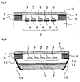
- Fig. 1 is a diagram, showing a schematic structure of a light receiving element according to the present embodiment.
- Such light receiving element includes a substrate 1, a light receiving element 2 provided on a surface of the substrate 1, a transparent cover 6 provided above such surface, and a sealing member 5, which is provided to fill a gap between the substrate 1 and the transparent cover 6 and adopted for providing a seal for the light receiving element 2 from the exterior thereof.
- the sealing member 5 is composed of a material containing a norbornene resin.
- the light receiving element 2 on the support 1 is presented by a two-dimensional array of pixel sensors composed of photoelectric regions 4 and microlenses 3, and this may alternatively have a standard configuration. An image resolution that the image sensor can be achieved is determined by the sizes and number of the pixel sensors, and the arrangement thereof ordinarily includes several hundreds to several thousands of pixel sensors per one column or one row.
- microlenses 3 are formed on the photoelectric region 4.
- the microlenses 3 are arranged corresponding to individual photoelectric regions 4, respectively.
- cylindrical optical lenses can be formed by, for example, comparting a layer composed of a transparent resin (including a photo resist) having a refractive index of 1.3 to 2.0 into predetermined geometries via a photolithographic processes or the like, and then melting the transparent resin of the respective compartments via a thermal processing, rounding a corner thereof by utilizing a surface tension and then cooling thereof.
- These microlenses 3 ordinarily have widths of about 2 to 6 ⁇ m, and heights of about 1 to 2 ⁇ m.
- the sealing member 5 contains a norbornene in resin, so that advantageous effects such as less absorbability of external moisture, less deterioration in the light-receiving ratio, better manufacturing stability and the like, can be obtained.
- the norbornene resin may be present uniformly over entire of the sealing member 5, or may be present locally in portions of the sealing member 5. It is preferable that the norbornene in resin is employed as a major constituent of the sealing member 5.
- a method for manufacturing the above-described light-receiving device will be described.
- a norbornene resin having epoxy group and a resin composition containing a crosslinker are applied by employing a spin coater and are dried to obtain a coating film.
- a transparent cover is disposed on such coating film, and then the entire thereof is heated to a temperature of 50 degree C to 250 degree C to join thereof. As such, the light-receiving device as shown in Fig. 1 is obtained.
- an epoxy resin is often conventionally employed for the above-described sealing member 5 in place of a cyclic olefin resin having epoxy group, and smaller difference in a refractive index between the light receiving element and the epoxy resin may causes a problem of losing focusing function, when the light receiving element is protected so as to be directly embedded in contact with the epoxy resin. Further, a problem of reducing a light-receiving ratio of the light receiving element may be occurred due to a deterioration of the epoxy resin on the light receiving element caused by a light for a long-term use.
- a norbornene resin having epoxy group is employed for the sealing member, so that the above-described deterioration of the resin can be considerably inhibited, and a suitable difference in the refractive index between the light receiving element and the epoxy resin can be ensured, leading to achieving a continuous sustainment of the focusing ability.
- Fig. 2 is a diagram, showing a schematic structure of a light receiving element according to the present embodiment.
- Such light receiving element includes a substrate 1, a light receiving element 2 provided on a surface of the substrate 1 and a transparent cover 6 provided above the surface thereof.
- a sealing member 5 composed of a material containing a norbornene resin is provided between the substrate 1 and the transparent cover 6.
- the sealing member 5 is provided to surround the light receiving element 2 in a position remote from the light receiving element 2, and joins the substrate 1 with the transparent cover 6 and has a hollow portion formed in the inner side thereof.
- the sealing member 5 is composed of a material containing a norbornene resin.
- the sealing member 5 functions as a spacer (dam) for forming a hollow structure between the transparent cover 6 and the light receiving element 2.
- the sealing member 5 may be joined to the transparent cover 6 through the adhesive agent 7 as shown in Fig. 3 .
- the sealing member 5 is composed of a norbornene resin having epoxy group, and more preferably composed of a photosensitive norbornene resin having epoxy group.
- An addition of a photosensitivity provides benefits such as an improved workability, higher location accuracy and higher uniformity in the dimensional height.
- the sealing member 5 containing the norbornene olefin resin having epoxy group is hard to absorb an external moisture, so that advantageous effects such as preventing a loss of transparency in the transparent cover 6 can be obtained.
- a photosensitive norbornene resin composition having epoxy group is applied on the semiconductor substrate provided with the microlenses 3 by employing a spin coater, and then, is heated and dried with a hot plate to obtain a coating film.
- An exposure to light is conducted over portions for forming a dam in the coating film, and then, is heated to a temperature of 50 degree C to 180 degree C for several minutes with a hot plate for accelerating a cross linking reaction.
- dipping in developer is conducted for about 30 seconds to dissolve to unexposed portions to remove thereof.
- a transparent cover is disposed on such coating film, and then the whole thereof is heated to a temperature of 50 degree C to 250 degree C to join thereof.
- an adhesive agent is applied on such coating film, and a transparent cover is disposed thereon, and joins thereof.
- a dam is formed so as to surround the light receiving element region, and thus the light-receiving device of residue-free on the microlenses 3 is manufactured.
- Fig. 3 and Fig. 4 are diagrams, showing a schematic structure of a light receiving element according to the present embodiment.
- Fig. 4 shows a cross-sectional view of a CMOS image sensor, which has a wafer level chip size package (CSP) structure that is a type of a light-receiving device shown in Fig. 3 and has a hollow structure of the present invention.
- CSP wafer level chip size package
- the sealing member 5 is disposed so as to surround the light receiving element 2 to join the substrate 1 with the transparent cover 6, and has a hollow portion formed in the inner side thereof.
- An upper portion of the sealing member 5 has a flat geometry, and a transparent cover is provided on the surface thereof through an adhesive agent 7, as required.
- the sealing member 5 is higher than the microlenses 3, and if the transparent cover 6 is provided on the upper surface of the sealing member 5, an air gap is formed between the microlenses 3 and the transparent cover 6.
- Such sealing member 5 has a height of about 5 to 40 ⁇ m and a width of 100 to 1,000 ⁇ m. Nonetheless, a considerably different geometry of the sealing member 5 may alternatively be employed according to various types of factors such as a size of a pixel sensor, a height of a microlens 3 and the like.
- a transparent cover 6 is bonded thereto by a heat.
- an adhesive agent 7 may be employed as required.
- a thermosetting adhesive agent 7 is applied on the upper surface of the sealing member 5.
- the adhesive agent 7 is selectively applied on the sealing member 5 via a screen printing process and the like, a transparent cover 6 is disposed on the sealing member 5, and then the adhesive agent 7 is cured via a thermal processing.
- the sealing member 5 having a predetermined height is provided to bond a wafer 10 serving as a support 1 and the transparent cover 6, so that a constant distance between the wafer 10 and the transparent cover 6 can be provided, leading to facilitating an alignment thereof.
- Such bonding process is preferably conducted in a vacuum or in an inert gas atmosphere such as nitrogen and the like.
- an interconnect is formed by employing, for example, a method for forming an electric lead that is employed in a shell case-type CSP, and the formed interconnect is diced into individual light receiving elements, and then separated into individual light-receiving devices, thereby obtaining the light-receiving device composed of the CSP as shown in Fig. 4 .
- the light-receiving device shown in Fig. 4 employs a glass substrate for the transparent cover 6.
- leads 13 joined to the electrode pads 11 extend to the back surface of the chip to achieve forming interconnects in the back surface thereof, such that a space for the interconnects can be considerably reduced, as compared with a package for joining the semiconductor chip via a wire bonding. Further, since employing such method achieves conducting the whole manufacturing process from forming the semiconductor device to packaging thereof under a wafer condition, leading to a considerably reduced manufacturing cost as compared with the conventional light-receiving devices.
- Cyclic olefin monomers available generally include: monocyclic compounds such as cyclohexene, cyclooctene and the like; and polycyclic compounds such as norbornene, norbornadiene, dicyclopentadiene, dihydrodicyclopentadiene, tetracyclododecen, tricyclopentadiene, dihydrotricyclopentadiene, tetracyclopentadiene, dihydrotetracyclopentadiene and the like. Substitution products having functional group bound to these monomers may alternatively be employed.
- Cyclic olefin resin available typically includes a polymer of the above-described cyclic olefin monomers.
- an available polymerization process includes a known process such as random polymerization, block polymerization and the like. Typical example may include (co)-polymer of norbornene type monomer, copolymer of norbornene type monomer and other types of monomers available for copolymerizing with ⁇ -olefins or the like, and hydrogenated products of these copolymers.
- These cyclic olefin resins may be manufactured by a known polymerization process, and such polymerization process typically includes an addition polymerization process and a ring-opening polymerization process.
- a norbornene resin is employed for the sealing member, benefits of providing an improved manufacturing stability such as achieving a higher precision of the patterning in the manufacture of the light-receiving device can be obtained.
- Typical addition polymer of cyclic olefin resin may include: (1) addition (co)-polymer of norbornene type monomer obtained by addition (co)-polymerizing norbornene type monomer; (2) addition copolymer of norbornene type monomer and ethylene or ⁇ -olefins; and (3) addition copolymer of norbornene type monomer and nonconjugated diene, and in addition with other type of monomer as required. These resins may be obtained with any of known polymerization processes.
- Typical ring-opened polymer of cyclic olefin resin may includes: (4) ring-opened (co)-polymer of norbornene type monomer, and in addition a resin of hydrogenated product of such (co)-polymer as required;(5) a ring-opened copolymer of norbornene type monomer and ethylene or ⁇ -olefins, and in addition a resin of hydrogenated product of such (co)-polymer as required; and (6) a ring-opened copolymer of norbornene type monomer and nonconjugated diene or other monomer and in addition a resin of hydrogenated product of such (co)-polymer as required. These resins may be obtained with any of known polymerization processes.
- a cyclic olefin resin preferably has reactive functional groups.
- reactive functional groups includes epoxy group such as glycidyl ether group and the like, oxetane group, carboxyl group, hydroxyl group, unsaturated bonds, amino group or the like. Epoxy group is particularly preferable among these groups.
- cyclic olefin resin having epoxy group can generally be obtained by directly polymerizing monomer containing epoxy group in its molecular
- similar polymer may also be obtained via a manner for introducing epoxy group in side-chain via a conversion reaction after the polymerization.
- Typical conversion reaction includes known manners such as: inducing a grafting reaction of the above-described polymer with unsaturated monomer containing epoxy group; inducing a reaction of reactive functional group site in the above-described polymer with compounds having epoxy group; inducing a direct epoxidation of the above-described polymer having carbon-carbon double bond in molecular by employing epoxidation agents such as peroxy acid, hydroperoxide, and the like.
- the addition polymer of a cyclic olefin resin is obtained by a coordination polymerization by utilizing a metal catalyst, or a radical polymerization.
- the polymer is obtained by polymerizing monomer in solution in the presence of a transition metal catalyst ( NiCOLE R. GROVE et al., Journal of Polymer Science: part B, Polymer Physics, Vol. 37, pp. 3003-3010 (1999 )).
- Nickel and the platinum catalysts typically employed metal catalysts in the coordination polymerization are described in PCT WO97/33,198 and PCT WO00/20,472 .
- Typical metal catalyst for the coordination polymerization includes known metal catalysts such as: (toluene) bis (perfluoro phenyl) nickel; (mesilene) bis (perfluorophenyl) nickel; (benzene) bis (perfluorophenyl) nickel; bis (tetrahydro) bis (perfluorophenyl) nickel; bis (ethyl acetate) bis (perfluorophenyl) nickel; bis (dioxane) bis (perfluorophenyl) nickel and the like.
- Typical radical polymerization technology is described in Encyclopedia of Polymer Science, John Wiley & Sons, 13, 708(1988 ). Radical polymerization is generally induced by reacting monomer in solution with elevating a temperature to 50 degree C to 150 degree C in the presence of a radical initiator.
- Typical radical initiator includes: azobis (isobutyronitrile) (AIBN); benzoyl peroxide; lauryl peroxide; azobis (iso captronitrile); azobis (isoleronitrile); t-butyl hydroperoxide or the like.
- the ring-opened polymer of a cyclic olefin resin is obtained by: ring-opening (co)-polymerizing at least one or more norbornene type monomer with a catalyst of titanium or tungsten compound via a known ring opening (co)-polymerization process to manufacture a ring-opening (co)-polymer; and then hydrogenating carbon-carbon double bond in the aforementioned ring-opening (co)-polymer via an ordinary hydrogenation process as required to manufacture a thermoplastic saturated norbornene resin.
- Suitable polymerization solvent of the above-described polymerization system includes hydrocarbons or aromatic solvents.
- Typical hydrocarbon solvent includes pentane, hexane, heptane, cyclohexane or the like, although it is not limited thereto.
- Typical aromatic solvent includes benzene, toluene, xylene, mesitylene or the like, although it is not limited thereto. Diethyl ether, tetrahydrofuran, ethyl acetate, esters, lactones, ketones, amides may also be employed. These solvents, alone or a combination thereof, may be employed as a polymerization solvent.
- Molecular weight of the cyclic olefin resin may be controlled by adjusting a ratio of an initiator and a monomer, or by adjusting a polymerization time.
- molecular weight can be controlled by employing a chain transfer catalyst.
- ⁇ -olefin such as ethylene, propylene, 1-hexane, 1-decene, 4-methyl -1-pentene and the like is suitable for controlling molecular weight.
- weight-average molecular weight is 10,000-500,000, preferably 80,000-200,000, and more preferably 100,000-125,000.
- Weight-average molecular weight may be measured via a gel permeation chromatography (GPC) employing normal polynorbornene (implemented in relation to ASTM DS 3536-91).
- alkyl group examples include methyl, ethyl, propyl, isopropyl, butyl, pentyl, hexyl, heptyl, octyl, nonyl, decyl, dodecyl, cyclopentyl, cyclohexyl, cyclo octyl, or the like
- alkenyl group examples include vinyl, allyl, butynyl, cyclohexyl or the like
- alkynyl group examples include ethynyl, 1-propynyl, 2-propynyl, 1-butynyl, 2-butynyl or the like
- specific examples of aryl group include phenyl, naphthyl, anthracenyl or the like
- specific group examples of aralkyl group include benzyl, phenethyl or the like, although it is not limited thereto.
- R 1 to R 4 are respectively any of functional group selected from hydrogen, alkyl group, alkenyl group, alkynyl group, allyl group, aryl group, aralkyl group, monovalent functional group having ester group, monovalent functional group having ketone group, monovalent functional group having ether group and monovalent functional group having epoxy group.
- R 1 to R 4 may be the same or different.
- at least one or more thereof is functional group having epoxy group.
- Typical cyclic olefin monomer employed for manufacturing a cyclic olefin resin includes, for example: monomer having alkyl group, such as 5-methyl -2-norbornene, 5-ethyl -2-norbornene, 5-propyl -2-norbornene, 5-butyl -2-norbornene, 5-pentyl -2-norbornene, 5-hexyl -2-norbornene, 5-heptyl -2-norbornene, 5-octyl -2-norbornene, 5-nonyl -2-norbornene, 5-decyl -2-norbornene and the like, monomer having alkenyl group such as 5-allyl -2-norbornene, 5-methylidene -2-norbornene, 5-ethylidene -2-norbornene, 5-isopropylidene -2-norbornene, 5-(2-propen
- the cyclic olefin resin having epoxy group employed is an addition (co)-polymer of norbornene type monomer, generally represented by formula (8).
- R 1 to R 4 are respectively any of functional group selected from hydrogen, alkyl group, alkenyl group, alkynyl group, allyl group, aryl group, aralkyl group, monovalent functional group having ester group, monovalent functional group having ketone group, monovalent functional group having ether group and monovalent functional group having epoxy group.
- R 1 to R 4 may be the same or different.
- at least one or more thereof is functional group having epoxy group.
- Polymers represented by formulae (9), (10) are preferable for the cyclic olefin resin having epoxy group in view of film properties after the cure.
- Norbornene monomer having aralkyl group is introduced to the polymer as represented by formula (10) to provide an improved solubility to polar solvents such as cyclopentanone or heptanone, which are employed as solvents of negative liquid developer, providing a benefit of improved workability.
- n and m are integer number of 1 or larger.
- R 1 to R 7 are respectively any of functional group selected from hydrogen, alkyl group, alkenyl group, alkynyl group, allyl group, aryl group, aralkyl group, monovalent functional group having ester group, monovalent functional group having ketone group, monovalent functional group having ether group and monovalent functional group having epoxy group.
- R 1 to R 7 may be the same or different.
- R 1 to R 10 are respectively any of functional group selected from hydrogen, alkyl group, alkenyl group, alkynyl group, allyl group, aryl group, aralkyl group, monovalent functional group having ester group, monovalent functional group having ketone group, monovalent functional group having ether group and monovalent functional group having epoxy group.
- R 1 to R 10 may be the same or different.
- Polymers represented by formula (11) are preferable for the cyclic olefin resin having epoxy group, in view of film properties after the cure.
- monomer having decyl group a film exhibiting lower modulus is obtained, and by introducing monomer having phenylethyl group, a film exhibiting lower moisture absorption, higher chemical resistance and higher polar solvent solubility is obtained.
- n and m are integer number of 1 or larger.
- Monomer having epoxy group in copolymer may be determined, so that cross-linkages are formed by an exposure to light and a suitable crosslink density for enduring against liquid developer is obtained.
- Available monomer content having epoxy group in polymer is 5 to 95 mol%, preferably 20 to 80 mol%, and more preferably 30 to 70 mol%.
- Polymer thus obtained exhibits improved mechanical properties such as lower moisture absorption ( ⁇ 0.3 %wt.), lower dielectric constant ( ⁇ 2.6), lower dielectric loss (0.001), glass transition temperature (170 to 400 degree C) or the like.
- the crosslinking agent employed for creating cross-linkages in a cyclic olefin resin having epoxy group is a compound generally known as a crosslinker, and for example, a curing agent that exhibits the capability thereof by heating thereof, or a photo reactive material may be employed.
- Typical curing agent that is capable of creating cross linkages in a cyclic olefin resin having epoxy group by heating includes aliphatic polyamine, alicycle polyamine, aromatic polyamine, bisazide, acid anhydride, dicarboxylic acid, polyphenol, polyamide and the like.
- Such curing agent includes, for example: aliphatic polyamines such as hexamethylene diamine, triethylenetetramine, diethylenetriamine, tetraethylenepentamine and the like; alicyclic polyamines such as diaminocyclohexane, 3 (4), 8 (9)-bis (aminomethyl) tricyclo[5,2,1,0 2,6 ] decane, 1,3-(diaminomethyl) cyclohexane, menthene diamine, isophorone diamine, N-aminoethyl piperazine, bis (4-amino-3-methylcyclohexyl) methane, bis (4-aminocyclohexyl) methane and the like; aromatic poly amines such as 4,4'-diaminodiphenyl ether, 4,4'-diaminodiphenyl methane, ⁇ , ⁇ '- bis (4-aminophenyl)-1,3-diisopropyl
- a photoacid generator may be employed for the photo reactive material. Any known photoacid generators may be employed.
- the photoacid generator provides cross linkage of epoxy group and provides an improved adhesiveness with a substrate by being cured thereafter.
- Preferable photoacid generator includes onium salt, halogenated compounds, sulfates and mixtures thereof.
- typical onium salt includes diazonium salt, ammonium salt, iodonium salt, sulfonium salt, phosphate, arsonium salt, oxonium salt or the like.
- counter anion there is no limitation of counter anion, as long as the compound is capable of creating a counter anion with onium salt as above described.
- Typical photoacid generator of onium salt includes triphenylsulfonium tetrafluoroborate, triphenyl sulfonium hexafluoro borate, triphenylsulfonium tetrafluoro arsenate, triphenylsulfonium tetrafluorophosphate, triphenylsulfonium tetrafluorosulfate, 4-thiophenoxy diphenylsulfonium tetrafluoroborate, 4-thiophenoxy diphenylsulfonium hexafluoro antimonate, 4- thiophenoxy diphenylsulfonium hexafluoroarsenate, 4- thiophenoxy diphenylsulfonium tetrafluoro phosphat
- photoacid generators having halogen except fluorine examples include 2,4,6-tris (trichloromethyl) triazine, 2-allyl-4,6-bis (trichloromethyl) triazine, ⁇ , ⁇ , ⁇ -tribromomethyl phenyl sulfone, ⁇ , ⁇ -2,3,5,6- hexachloroxylene, 2,2- bis (3,5-dibromo-4-hydroxyphenyl) -1,1,1,3,3,3- hexafluoroxylene, 1,1,1- tris (3,5-dibromo-4- hydroxyphenyl) ethane and mixtures thereof.
- Typical sulfonate-type photoacid generator includes 2-nitrobenzyl tosylate, 2,6- dinitrobenzyl tosylate, 2,4-dinitrobenzyl tosylate, 2- nitrobenzyl methyl sufonate, 2-nitrobenzyl acetate, 9,10- dimethoxy anthracene -2 -sulfonate, 1,2,3- tris (methanesulfonyloxy) benzene, 1,2,3- tris (ethane sulfonyloxy) benzene, 1,2,3- tris (propanesulfonyloxy) benzene or the like, though it is not limited thereto.
- Preferable photoacid generator includes 4,4'-di- t-butylphenyliodonium triflate, 4,4',4"-tris (t- butylphenyl) sulfonium triflate, diphenyliodonium tetrakis (pentafluorophenyl) borate, triphenyl sulfonium diphenyliodonium tetrakis (pentafluorophenyl) borate, 4,4'-di-t- butylphenyl iodonium tetrakis (pentafluorophenyl) borate, tris (t-butylphenyl) sulfonium tetrakis (pentafluorophenyl) borate, (4-methylphenyl)-4 -(1-methylethyl) phenyl iodonium tetrakis (pentafluorophenyl) borate and mixtures
- the crosslinker of the present invention may be appropriately selected according to an assembly process for a light-receiving device.
- the assembly process includes a developing and exposure operations, it is necessary to employ a photo reactive material for the crosslinker.
- a curing agent or a photo reactive material may be employed.
- a sensitizer may be employed for the cyclic olefin resin composition as required, in order to enhance exposure properties.
- the sensitizer is capable of providing availability of increased range of wave length that can activate a photoacid generator, and can be added with a range of providing no direct influence on the cross linking reaction of polymer.
- a photo sensitizer is a compound, which exhibits a maximum absorption constant near that of the employed light source and is capable of effectively providing an absorbed energy to the photoacid generator.
- Typical sensitizer for the photoacid generator includes polycyclic aromatic compounds such as anthracene, pyrene, parylene and the like.
- Blending ratio of the photoacid generator in the present invention is typically from 0.1 to 10 parts by weight for 100 parts by weight of the polymer, and more preferably from 0.2 to 5 parts by weight.
- sensitizer is effective to activate the photoacid generator.
- the acid scavenger absorbs an acid diffusing to an unexposed portion during a photochemical reaction.
- Typical acid scavenger includes pyridine, lutidine, phenothiazine, and secondary and tertiary amines such as tri-n-propyl amine, triethylamine and the like, though it is not limited thereto.
- Blending ratio of the acid scavenger is typically from 0.01 to 0.05 parts by weight for 100 parts by weight of the polymer.
- additives such as a leveling agent, an antioxidant, a fire retardant agent, a plasticizer, a silane coupling agent and the like may be added, as required.
- Non-reactive solvents include non-reactive solvents and reactive solvents, and the non-reactive solvent functions as a carrier for polymers and additives, and are removable in the coating or cure process.
- the reactive solvent includes reactive group exhibiting a compatibility with a curing agent, which is added in the resin composition.
- Typical non-reactive solvent includes hydrocarbons and aromatic compounds. Examples thereof include hydrocarbon solvent of alkane or cycloalkane such as pentane, hexane, heptane, cyclohexane, decahydronaphthalene and the like, though it is not limited thereto.
- aromatic solvents include benzene, toluene, xylene, mesitylene and the like. Diethyl ether, tetrahydrofuran, anisole, acetate, ester, lactone, ketone or amide are also useful.
- Available reactive solvents include cycloether compound such as cyclohexene oxide or ⁇ -pinene oxide, aromatic cycloether such as [methylene bis (4,1- phenylene oxy methylene)] bis oxirane and the like, alicyclic vinyl ether compound such as 1,4-cyclohexane dimethanol divinyl ether and the like, and aromatic compound such as bis (4-vinylphenyl) methane and the like, which may be employed alone or in a form of mixture thereof.
- Preferable compounds are mesitylene and decahydronaphthalene, and these are optimum for applying resins on a substrate of such as silicon, silicon oxide, silicon nitride, silicon oxynitride, of and the like.
- Resin solid content in the resin composition employing in the present invention is about 5 to 60 %wt. Further, preferably, it is about 30 to 55 %wt., and more preferably, it is about 35 to 45 %wt.
- Solution viscosity is 10 to 25,000 cP, and more preferably 100 to 3,000 cP.
- a resin composition may be obtained by simply mixing a cyclic norbornene resin having epoxy group and a photoacid generator, and additionally a solvent, a sensitizer, an acid scavenger, a leveling agent, an antioxidant, a fire retardant agent, a plasticizer, a silane coupling agent and the like as required.
- a process for preparing a semiconductor device of the present invention will be described. First of all, a norbornene resin composition is coated on a suitable support of, for example, a silicon wafer, a ceramic, an aluminum substrate or the like.
- Typical application process includes a spin-coating process employing a spinner, a spray-coating process employing a spraying coater, a dipping process, a printing process, a roll coating process or the like.
- a pre-baking process is conducted at 90 to 140 degree C to dry the coated film, and then, a chemical ray is irradiated to a desired pattern geometry.
- Available chemical ray includes x-ray, electron beam, ultra-violet ray, visible ray or the like, and those having a wave length of 200 to 700 nm are preferable.
- a bake process is conducted. Such operation lets rate of reaction of epoxy cross linking increase.
- Typical baking condition is 50 to 200 degree C, preferably 80 to 150 degree C, and more preferably 90 to 130 degree C.
- Typical developer includes hydrocarbon-containing solvents including alkane and cycloalkane such as pentane, hexane, heptane, cyclohexane and the like, and aromatic hydrocarbon-containing solvents such as toluene, mesitylene, xylene, mesitylene and the like.
- terpenes such as limonene, dipentene, pinene, menthane and the like, and ketones such as cyclopentanone, cyclohexanone, 2 -heptanone and the like may be employed, and an organic solvent containing a suitable amount of surfactants added therein may be preferably employed.
- Available developing processes include manners utilizing spraying, paddling, dipping, ultrasonic wave and the like.
- the relief pattern formed by the developing process is rinsed.
- An alcohol is employed for a rinse solution.
- a heat treatment process is conducted at 50 to 200 degree C to remove the developer and the rinse solution, and further, cross-linking of epoxy group is completed to obtain a finished pattern that can exhibits better thermal resistance.
- the adhesive agent employed in the present invention is preferably composed of silica filler and epoxy resin that is in liquid state at an ambient temperature and a curing agent, and preferably contains 1 to 10 %wt. of silica filler (A) in the component and such silica filler is ultra fine particle silica powder having a mean particle diameter of 2 to 500 nm.
- the epoxy resin employed in the present invention is limited to liquid at an ambient temperature, and if it is not liquid at an ambient temperature, solvent is additionally needed for kneading with silica filler. The additional solvent causes a generation of voids, which is not preferable as it reduces the adhesive strength and the thermal conductivity of the cured material.
- Typical epoxy resins include, for example, bisphenol A, bisphenol F, a compound in liquid state at an ambient temperature such as polyglycidyl ether obtained by a reaction of novolac phenol with epichlorohydrin, vinylcyclohexene dioxide, dicyclopentadiene dioxide, and alicyclic epoxy such as alicyclic diepoxy-azipate, or one of these may be employed or two or more of these may be employed, though it is not limited thereto.
- bisphenol A bisphenol F
- a compound in liquid state at an ambient temperature such as polyglycidyl ether obtained by a reaction of novolac phenol with epichlorohydrin, vinylcyclohexene dioxide, dicyclopentadiene dioxide, and alicyclic epoxy such as alicyclic diepoxy-azipate, or one of these may be employed or two or more of these may be employed, though it is not limited thereto.
- a standard epoxy resin such as n-butyl glycidyl ether, versatic acid glycidyl ester, styrene oxide, phenylglycidyl ether, cresyl glycidyl ether, butylphenyl glycidyl ether and the like may also be employed.
- a simultaneous use of bisphenol F and a latent amine compound such as dicyandiamide, adipic acid hydrazide and the like is preferable, it is preferable to contain bisphenol F with an amount of 2 to 30 %wt. in the adhesive agent.
- the amount of lower than 2 %wt. provides excessively lower blending quantity, leading to an insufficient adhesive strength, and the amount of larger than 30 %wt. provides excessive amount of phenolic hydroxyl group over epoxy group, leading to remaining unreacted phenolic hydroxyl group in the cured product, and thus these are not preferable.
- the silica filler employed in the present invention preferably composed of ultra fine particle silica powder having a mean particle diameter of 2 to 500 nm contained in the adhesive agents at 1 to 10 %wt.
- the amount of the whole silica filler in the adhesive agent of larger than 1 %wt. eliminates problems in the application such as a dripping of a paste, and the amount of lower than 10 %wt. improves the workability, which is otherwise deteriorated by a plugging of a mask for screen printing or the like.
- additives such as a cure accelerator, a flexibility-applying agent, a pigment, a dye, an antifoaming agent and the like may be employed as required in the adhesive agent employed in the present invention.
- the manufacturing method of the present invention includes, for example, pre-mixing respective components, kneading thereof by employing a triple roller to obtain a paste, and defoaming thereof in a vacuum, and the like.
- Ethyl acetate (917 g), cyclohexane (917 g), decyl norbornene (192 g, 0.82 mol) and glycidyl methyl ether norbornene (62 g, 0.35 mol) were added to a reaction flask.
- the reaction flask was taken out from the glove box, and dried nitrogen gas was introduced therein.
- Intermediate product was degassed by flowing nitrogen gas through a solution thereof for 30 minutes.
- Such insulating resin paste was defoamed in a vacuum chamber at 2 mmHg for 30 minutes to obtain an adhesive agent.
- the above-described cyclic olefin resin composition was applied by employing a spin coater, and then was dried with a hot plate at 110 degree C for 5 minutes to obtain a coating film having a film thickness of about 40 ⁇ m.
- An exposure was conducted for portions for forming dams over such coating film through a reticle with a broadband stepper exposure machine (commercially available from ULTRATEC Co., Ltd.) at 1,500 mJ/cm 2 . Thereafter, it was heated with a hot plate at 90 degree C for 4 minutes, for accelerating a cross linking reaction of the exposed portion.
- the above-described adhesive agent was applied on the formed dams via a screen printing process, and then, the glass substrate is disposed on the dams, a curing was conducted at 100 degree C for 60 minutes to adhere the glass substrate with the dams.
- interconnects were formed by employing a method for forming an electric lead that is employed in a shell case-type CSP, and were diced into individual light receiving elements to obtain the light-receiving device. It was confirmed that the obtained light-receiving device exhibited no obstacle in operating as the light-receiving device.
- the above-described cyclic olefin resin composition was coated by employing a spin coater, and then was dried with a hot plate at 110 degree C for 5 minutes to obtain a coating film having a film thickness of about 40 ⁇ m.
- An exposure was conducted for portions for forming dams over such coating film through a reticle with a broadband stepper exposure machine (commercially available from ULTRATEC Co., Ltd.) at 1,500 mJ/cm 2 . Thereafter, it was heated with a hot plate at 90 degree C for 4 minutes, for accelerating a cross linking reaction of the exposed portion.
- dams were formed in locations remote from the light receiving elements so as to surround the light receiving elements, and it was confirmed that no residue was found on the microlenses. Further, absolutely no pattern delamination was observed in the remained pattern, and found to have an improved adhesiveness in the developing process.
- a glass substrate is disposed on the formed dams, and a curing was conducted at 160 degree C for 30 minutes while pressuring at 80 kPa to have the glass substrate adhere with the semiconductor substrate. The moisture absorption of such cured film was 0.2 %.
- interconnects were formed by employing a method for forming an electric lead that is employed in a shell case-type CSP, and were diced into individual light receiving elements to obtain the light-receiving device. It was confirmed that the obtained light-receiving device exhibited no obstacle in operating as the light-receiving device.
- the above-described cyclic olefin resin composition was coated by employing a spin coater, and then was dried with a hot plate at 110 degree C for 5 minutes to obtain a coating film having a film thickness of about 10 ⁇ m.
- a glass substrate is disposed on the coating film, and a curing was conducted at 160 degree C for 30 minutes while pressuring at 80 kPa to have the glass substrate adhere with the semiconductor substrate.
- the moisture absorption of such cured film was 0.2 %.
- interconnects were formed by employing a method for forming an electric lead that is employed in a shell case-type CSP, and were diced into individual light receiving elements to obtain the light-receiving device. It was confirmed that the obtained light-receiving device exhibited no obstacle in operating as the light-receiving device.
- the present invention is not limited as described above, and various configurations are also included.
- the present invention includes the following configurations.
- a light-receiving device that is, composed of: a semiconductor substrate including at least one light receiving element; a dam surrounding the light receiving element provided on the semiconductor substrate; an adhesive agent layer provided on the dam; and a transparent cover provided on the adhesive agent layer, wherein the dam includes a norbornene resin having epoxy group and a photoacid generator.
- R 1 to R 4 may be respectively any of functional groups selected from hydrogen, alkyl group, alkenyl group, alkynyl group, allyl group, aryl group, aralkyl group, functional group having ester group, functional group having ketone group, monovalent functional group having ether group and monovalent functional group having epoxy group.
- R 1 to R 4 may be different in repeated monomers, while at least one or more thereof is a functional group having epoxy group among R 1 to R 4 contained in the whole repeated units.
- R 1 to R 7 may be respectively any of functional groups selected from hydrogen, alkyl group, alkenyl group, alkynyl group, allyl group, aryl group, aralkyl group, functional group having ester group, functional group having ketone group and monovalent functional group having ether group.
- R 1 to R 7 may be different in repeated monomers.
- R 1 to R 10 may be respectively any of functional group selected from hydrogen, alkyl group, alkenyl group, alkynyl group, allyl group, aryl group, aralkyl group, functional group having ester group, functional group having ketone group and monovalent functional group having ether group.
- R 1 to R 10 may be different in repeated monomers.
- the light-receiving device as set forth in [1] to [5], wherein the semiconductor substrate described in [1] is silicon, and the light receiving element includes the CMOS image sensor apparatus having microlenses disposed therein.
- the light-receiving device as set forth in [1] to [7], wherein the adhesive agent constituting the aforementioned adhesive agent layer is composed of silica filler (A), an epoxy resin that is liquid at an ambient temperature (B) and curing agent (C).
- the adhesive agent constituting the aforementioned adhesive agent layer is composed of silica filler (A), an epoxy resin that is liquid at an ambient temperature (B) and curing agent (C).
- mean particle diameter of the silica filler in the aforementioned adhesive agent (A) is 2 to 500 nm.
Landscapes
- Solid State Image Pick-Up Elements (AREA)
- Light Receiving Elements (AREA)
- Compositions Of Macromolecular Compounds (AREA)
- Transforming Light Signals Into Electric Signals (AREA)
- Addition Polymer Or Copolymer, Post-Treatments, Or Chemical Modifications (AREA)
- Geophysics And Detection Of Objects (AREA)
- Measuring Fluid Pressure (AREA)
- Optical Radar Systems And Details Thereof (AREA)
Claims (12)
- Lichtempfangsvorrichtung, umfassend:ein Substrat (1),ein Lichtempfangselement (2), das auf einer Oberfläche des Substrats bereitgestellt wird,eine transparente Abdeckung (6), die über der Oberfläche des Substrats bereitgestellt wird, undein Abdichtungselement (5), um eine Abdichtung für das Lichtempfangselement gegenüber einer Außenseite bereitzustellen, wobei das Abdichtungselement zumindest in einem Umkreis des Lichtempfangselements zwischen dem Substrat und der transparenten Abdeckung bereitgestellt wird,dadurch gekennzeichnet, dass das Abdichtungselement ein Norbornenharz enthält.
- Lichtempfangsvorrichtung wie in Anspruch 1 dargelegt, wobei das Abdichtungselement bereitgestellt wird, um das Lichtempfangselement in einer Position abseits des Lichtempfangselements zu umgeben.
- Lichtempfangsvorrichtung wie in Anspruch 1 dargelegt, wobei das Abdichtungselement bereitgestellt wird, um eine Lücke zwischen dem Substrat und der transparenten Abdeckung zu füllen.
- Lichtempfangsvorrichtung wie in Anspruch 1 dargelegt, wobei das Abdichtungselement eine verbrückte Verbindung des Norbornenharzes mit Epoxygruppe ist.
- Lichtempfangsvorrichtung wie in Anspruch 4 dargelegt, wobei das Norbornenharz mit Epoxygruppe eine Wiederholungseinheit der Formel (1) aufweist:

- Lichtempfangsvorrichtung wie in Anspruch 4 dargelegt, wobei das Norbornenharz mit Epoxygruppe Wiederholungseinheiten der Formel (2) bzw. der Formel (3) aufweist:

- Lichtempfangsvorrichtung wie in Anspruch 4 dargelegt, wobei das Norbornenharz mit Epoxygruppe eine Wiederholungseinheit der Formeln (4), (5) und (6) aufweist:

- Lichtempfangsvorrichtung wie in Anspruch 1 dargelegt, wobei eine Dicke des Abdichtungselements dicker als eine Vorsprungshöhe des Lichtempfangselements von dem Substrat ist.
- Lichtempfangsvorrichtung wie in Anspruch 1 dargelegt, wobei das Abdichtungselement und die transparente Abdeckung über eine Haftvermittlerschicht (7) verbunden sind.
- Lichtempfangsvorrichtung wie in Anspruch 9 dargelegt, wobei die Haftvermittlerschicht durch Aushärtung des Haftvermittlers ausgebildet wird, welcher aus einem Silicafüllmaterial und einem Epoxyharz, das bei Umgebungstemperatur in flüssiger Form vorliegt, und einem Aushärtemittel zusammengesetzt ist.
- Lichtempfangsvorrichtung wie in Anspruch 10 dargelegt, wobei der Haftvermittler 1 bis 10 Gew.-% des Silicafüllmaterials beinhaltet.
- Lichtempfangsvorrichtung wie in Anspruch 10 dargelegt, wobei der mittlere Partikeldurchmesser des Silicafüllmaterials 2 bis 500 nm beträgt.
Applications Claiming Priority (3)
| Application Number | Priority Date | Filing Date | Title |
|---|---|---|---|
| JP2004298670 | 2004-10-13 | ||
| JP2005252886 | 2005-08-31 | ||
| PCT/JP2005/018466 WO2006040986A1 (ja) | 2004-10-13 | 2005-10-05 | 受光装置 |
Publications (3)
| Publication Number | Publication Date |
|---|---|
| EP1804296A1 EP1804296A1 (de) | 2007-07-04 |
| EP1804296A4 EP1804296A4 (de) | 2008-02-20 |
| EP1804296B1 true EP1804296B1 (de) | 2008-10-01 |
Family
ID=36148281
Family Applications (1)
| Application Number | Title | Priority Date | Filing Date |
|---|---|---|---|
| EP05790435A Expired - Lifetime EP1804296B1 (de) | 2004-10-13 | 2005-10-05 | Lichtempfangseinrichtung |
Country Status (8)
| Country | Link |
|---|---|
| US (1) | US20090008682A1 (de) |
| EP (1) | EP1804296B1 (de) |
| JP (2) | JP4760713B2 (de) |
| KR (1) | KR100892204B1 (de) |
| AT (1) | ATE409960T1 (de) |
| DE (1) | DE602005010107D1 (de) |
| TW (1) | TWI483389B (de) |
| WO (1) | WO2006040986A1 (de) |
Cited By (1)
| Publication number | Priority date | Publication date | Assignee | Title |
|---|---|---|---|---|
| US20130061925A1 (en) * | 2010-05-17 | 2013-03-14 | Nippon Kayaku Kabushiki Kaisha | Photoelectric Conversion Element Using Thermosetting Sealing Agent For Photoelectric Conversion Element |
Families Citing this family (17)
| Publication number | Priority date | Publication date | Assignee | Title |
|---|---|---|---|---|
| JP2007311454A (ja) * | 2006-05-17 | 2007-11-29 | Sony Corp | 固体撮像装置 |
| WO2008023827A1 (en) | 2006-08-25 | 2008-02-28 | Sanyo Electric Co., Ltd. | Semiconductor device |
| US8148811B2 (en) * | 2006-08-25 | 2012-04-03 | Semiconductor Components Industries, Llc | Semiconductor device and manufacturing method thereof |
| WO2008023824A1 (fr) * | 2006-08-25 | 2008-02-28 | Sanyo Electric Co., Ltd. | Dispositif à semi-conducteur et son procédé de fabrication |
| DE102007001518B4 (de) * | 2007-01-10 | 2016-12-15 | Fraunhofer-Gesellschaft zur Förderung der angewandten Forschung e.V. | Vorrichtung und Verfahren zum Häusen eines mikromechanischen oder mikrooptoelektronischen Systems |
| JP2008235490A (ja) * | 2007-03-19 | 2008-10-02 | Sumitomo Bakelite Co Ltd | 中空構造体の製造方法および中空構造体 |
| US20100193122A1 (en) * | 2007-06-19 | 2010-08-05 | Sumitomo Bakelite Co., Ltd. | Process for manufacturing electronic device |
| JP5338663B2 (ja) * | 2007-06-19 | 2013-11-13 | 住友ベークライト株式会社 | 電子装置の製造方法 |
| JP5088373B2 (ja) * | 2007-08-10 | 2012-12-05 | 株式会社村田製作所 | 電子部品の製造方法 |
| JP5656349B2 (ja) * | 2007-09-20 | 2015-01-21 | プロメラス, エルエルシー | チップを積層するために、そしてチップ及びウェハを接合させるために有用な方法及び材料 |
| JP5344336B2 (ja) * | 2008-02-27 | 2013-11-20 | 株式会社ザイキューブ | 半導体装置 |
| US20120187553A1 (en) * | 2009-09-09 | 2012-07-26 | Sumitomo Bakelite Company Limited | Method of manufacturing semiconductor wafer bonding product, semiconductor wafer bonding product and semiconductor device |
| EP2619799A1 (de) * | 2010-09-22 | 2013-07-31 | Dow Corning Corporation | Elektronischer artikel und verfahren zu seiner herstellung |
| JP5634380B2 (ja) | 2011-10-31 | 2014-12-03 | アオイ電子株式会社 | 受光装置およびその製造方法 |
| SG11201403550YA (en) * | 2012-01-16 | 2014-09-26 | Promerus Llc | Thermo-oxidatively stable, side chain polyether functionalized polynorbornenes for microelectronic and optoelectronic devices and assemblies thereof |
| KR102075809B1 (ko) * | 2012-01-25 | 2020-02-10 | 소니 주식회사 | 광전 변환 소자, 광전 변환 소자의 제조 방법, 고체 촬상 장치 및 전자 기기 |
| TWI678387B (zh) * | 2014-08-26 | 2019-12-01 | 日商琳得科股份有限公司 | 硬化性組合物、硬化性組合物之製造方法、硬化物、硬化性組合物之使用方法以及光裝置 |
Family Cites Families (14)
| Publication number | Priority date | Publication date | Assignee | Title |
|---|---|---|---|---|
| US6833180B1 (en) * | 1997-07-04 | 2004-12-21 | Nippon Zeon Company, Ltd. | Adhesive for semiconductor part |
| DE19964228B4 (de) * | 1998-09-08 | 2008-11-13 | Fujitsu Ltd., Kawasaki | Verfahren zur Herstellung eines Reflexionsfilms und Herstellung optischer Vorrichtungen die einen Reflexionsfilm verwenden |
| US6335479B1 (en) * | 1998-10-13 | 2002-01-01 | Dai Nippon Printing Co., Ltd. | Protective sheet for solar battery module, method of fabricating the same and solar battery module |
| TW575632B (en) * | 2000-07-13 | 2004-02-11 | Ngk Spark Plug Co | Paste for filling throughhole and printed wiring board using same |
| TW499460B (en) * | 2000-10-06 | 2002-08-21 | Ind Tech Res Inst | Resin composition with excellent dielectric property |
| JP3839271B2 (ja) * | 2001-05-01 | 2006-11-01 | 富士写真フイルム株式会社 | 固体撮像装置及びその製造方法 |
| JP2003147321A (ja) * | 2001-11-09 | 2003-05-21 | Fujitsu Ltd | 接着剤 |
| CN1315950C (zh) * | 2002-06-20 | 2007-05-16 | 住友电木株式会社 | 透明复合材料组合物 |
| US6744109B2 (en) * | 2002-06-26 | 2004-06-01 | Agilent Technologies, Inc. | Glass attachment over micro-lens arrays |
| US7022790B2 (en) * | 2002-07-03 | 2006-04-04 | Sumitomo Bakelite Company, Ltd. | Photosensitive compositions based on polycyclic polymers |
| JP5030360B2 (ja) * | 2002-12-25 | 2012-09-19 | オリンパス株式会社 | 固体撮像装置の製造方法 |
| JP2004277726A (ja) * | 2003-02-27 | 2004-10-07 | Sumitomo Bakelite Co Ltd | 樹脂組成物および樹脂組成物の製造方法 |
| WO2005020328A1 (ja) * | 2003-08-22 | 2005-03-03 | Konica Minolta Opto, Inc. | 固体撮像装置及び該固体撮像装置を備えた撮像装置並びに固体撮像装置のマイクロレンズアレイ製造方法 |
| US7875686B2 (en) * | 2004-08-18 | 2011-01-25 | Promerus Llc | Polycycloolefin polymeric compositions for semiconductor applications |
-
2005
- 2005-10-05 AT AT05790435T patent/ATE409960T1/de not_active IP Right Cessation
- 2005-10-05 DE DE602005010107T patent/DE602005010107D1/de not_active Expired - Lifetime
- 2005-10-05 US US11/664,919 patent/US20090008682A1/en not_active Abandoned
- 2005-10-05 EP EP05790435A patent/EP1804296B1/de not_active Expired - Lifetime
- 2005-10-05 WO PCT/JP2005/018466 patent/WO2006040986A1/ja not_active Ceased
- 2005-10-05 JP JP2006540897A patent/JP4760713B2/ja not_active Expired - Fee Related
- 2005-10-05 KR KR1020077010177A patent/KR100892204B1/ko not_active Expired - Fee Related
-
2006
- 2006-01-26 TW TW095103686A patent/TWI483389B/zh not_active IP Right Cessation
-
2011
- 2011-04-11 JP JP2011087095A patent/JP2011199294A/ja active Pending
Cited By (1)
| Publication number | Priority date | Publication date | Assignee | Title |
|---|---|---|---|---|
| US20130061925A1 (en) * | 2010-05-17 | 2013-03-14 | Nippon Kayaku Kabushiki Kaisha | Photoelectric Conversion Element Using Thermosetting Sealing Agent For Photoelectric Conversion Element |
Also Published As
| Publication number | Publication date |
|---|---|
| ATE409960T1 (de) | 2008-10-15 |
| WO2006040986A1 (ja) | 2006-04-20 |
| KR20070067184A (ko) | 2007-06-27 |
| JPWO2006040986A1 (ja) | 2008-05-15 |
| TWI483389B (zh) | 2015-05-01 |
| KR100892204B1 (ko) | 2009-04-07 |
| EP1804296A4 (de) | 2008-02-20 |
| TW200709406A (en) | 2007-03-01 |
| US20090008682A1 (en) | 2009-01-08 |
| DE602005010107D1 (de) | 2008-11-13 |
| JP4760713B2 (ja) | 2011-08-31 |
| JP2011199294A (ja) | 2011-10-06 |
| EP1804296A1 (de) | 2007-07-04 |
Similar Documents
| Publication | Publication Date | Title |
|---|---|---|
| JP2011199294A (ja) | 受光装置 | |
| US8268540B2 (en) | Method of manufacturing light receiving device | |
| US7915467B2 (en) | Semiconductor wafer and semiconductor device | |
| WO2016035593A1 (ja) | 樹脂および感光性樹脂組成物 | |
| US20100120937A1 (en) | Semiconductor device | |
| JP4428189B2 (ja) | 樹脂封止型半導体装置 | |
| JP4170277B2 (ja) | 感光性樹脂組成物および半導体装置 | |
| WO2016063908A1 (ja) | 感光性接着剤組成物および半導体装置 | |
| JP4613763B2 (ja) | ポジ型感光性樹脂組成物、およびそれを用いたパターン形成方法、半導体装置、半導体装置の製造方法、表示体装置、表示体装置の製造方法 | |
| JP5304592B2 (ja) | 樹脂封止型半導体装置 | |
| JP5338459B2 (ja) | 感光性樹脂組成物、および半導体装置 | |
| JP2007078812A (ja) | 感光性樹脂組成物、それを用いた半導体装置、表示素子 | |
| JP2006096812A (ja) | 半導体表面保護膜用樹脂組成物、及びそれを用いた半導体装置 | |
| JP4412136B2 (ja) | 半導体表面保護膜用樹脂組成物、及びそれを用いた半導体装置 | |
| CN100521218C (zh) | 光接收装置 | |
| JP2007078781A (ja) | 感光性樹脂組成物 | |
| JP2007078820A (ja) | 感光性樹脂組成物、それを用いた半導体装置、表示素子 | |
| JP2013048295A (ja) | 樹脂封止型半導体装置 | |
| JP4556598B2 (ja) | 半導体装置 | |
| JP2006098949A (ja) | 半導体装置 | |
| JP4325531B2 (ja) | 樹脂封止型半導体装置 | |
| JP2009301056A (ja) | 半導体表面保護膜用樹脂組成物、及びそれを用いた半導体装置 | |
| JP2006108179A (ja) | 半導体装置 |
Legal Events
| Date | Code | Title | Description |
|---|---|---|---|
| PUAI | Public reference made under article 153(3) epc to a published international application that has entered the european phase |
Free format text: ORIGINAL CODE: 0009012 |
|
| 17P | Request for examination filed |
Effective date: 20070330 |
|
| AK | Designated contracting states |
Kind code of ref document: A1 Designated state(s): AT BE BG CH CY CZ DE DK EE ES FI FR GB GR HU IE IS IT LI LT LU LV MC NL PL PT RO SE SI SK TR |
|
| DAX | Request for extension of the european patent (deleted) | ||
| A4 | Supplementary search report drawn up and despatched |
Effective date: 20080117 |
|
| GRAP | Despatch of communication of intention to grant a patent |
Free format text: ORIGINAL CODE: EPIDOSNIGR1 |
|
| GRAS | Grant fee paid |
Free format text: ORIGINAL CODE: EPIDOSNIGR3 |
|
| GRAA | (expected) grant |
Free format text: ORIGINAL CODE: 0009210 |
|
| AK | Designated contracting states |
Kind code of ref document: B1 Designated state(s): AT BE BG CH CY CZ DE DK EE ES FI FR GB GR HU IE IS IT LI LT LU LV MC NL PL PT RO SE SI SK TR |
|
| REG | Reference to a national code |
Ref country code: GB Ref legal event code: FG4D |
|
| REG | Reference to a national code |
Ref country code: CH Ref legal event code: EP |
|
| REG | Reference to a national code |
Ref country code: IE Ref legal event code: FG4D |
|
| REF | Corresponds to: |
Ref document number: 602005010107 Country of ref document: DE Date of ref document: 20081113 Kind code of ref document: P |
|
| PG25 | Lapsed in a contracting state [announced via postgrant information from national office to epo] |
Ref country code: SI Free format text: LAPSE BECAUSE OF FAILURE TO SUBMIT A TRANSLATION OF THE DESCRIPTION OR TO PAY THE FEE WITHIN THE PRESCRIBED TIME-LIMIT Effective date: 20081001 |
|
| PG25 | Lapsed in a contracting state [announced via postgrant information from national office to epo] |
Ref country code: AT Free format text: LAPSE BECAUSE OF FAILURE TO SUBMIT A TRANSLATION OF THE DESCRIPTION OR TO PAY THE FEE WITHIN THE PRESCRIBED TIME-LIMIT Effective date: 20081001 Ref country code: BG Free format text: LAPSE BECAUSE OF FAILURE TO SUBMIT A TRANSLATION OF THE DESCRIPTION OR TO PAY THE FEE WITHIN THE PRESCRIBED TIME-LIMIT Effective date: 20090101 Ref country code: ES Free format text: LAPSE BECAUSE OF FAILURE TO SUBMIT A TRANSLATION OF THE DESCRIPTION OR TO PAY THE FEE WITHIN THE PRESCRIBED TIME-LIMIT Effective date: 20090112 Ref country code: LT Free format text: LAPSE BECAUSE OF FAILURE TO SUBMIT A TRANSLATION OF THE DESCRIPTION OR TO PAY THE FEE WITHIN THE PRESCRIBED TIME-LIMIT Effective date: 20081001 |
|
| PG25 | Lapsed in a contracting state [announced via postgrant information from national office to epo] |
Ref country code: PT Free format text: LAPSE BECAUSE OF FAILURE TO SUBMIT A TRANSLATION OF THE DESCRIPTION OR TO PAY THE FEE WITHIN THE PRESCRIBED TIME-LIMIT Effective date: 20090302 Ref country code: PL Free format text: LAPSE BECAUSE OF FAILURE TO SUBMIT A TRANSLATION OF THE DESCRIPTION OR TO PAY THE FEE WITHIN THE PRESCRIBED TIME-LIMIT Effective date: 20081001 Ref country code: IS Free format text: LAPSE BECAUSE OF FAILURE TO SUBMIT A TRANSLATION OF THE DESCRIPTION OR TO PAY THE FEE WITHIN THE PRESCRIBED TIME-LIMIT Effective date: 20090201 Ref country code: LV Free format text: LAPSE BECAUSE OF FAILURE TO SUBMIT A TRANSLATION OF THE DESCRIPTION OR TO PAY THE FEE WITHIN THE PRESCRIBED TIME-LIMIT Effective date: 20081001 Ref country code: MC Free format text: LAPSE BECAUSE OF NON-PAYMENT OF DUE FEES Effective date: 20081031 |
|
| REG | Reference to a national code |
Ref country code: IE Ref legal event code: MM4A |
|
| PG25 | Lapsed in a contracting state [announced via postgrant information from national office to epo] |
Ref country code: RO Free format text: LAPSE BECAUSE OF FAILURE TO SUBMIT A TRANSLATION OF THE DESCRIPTION OR TO PAY THE FEE WITHIN THE PRESCRIBED TIME-LIMIT Effective date: 20081001 Ref country code: EE Free format text: LAPSE BECAUSE OF FAILURE TO SUBMIT A TRANSLATION OF THE DESCRIPTION OR TO PAY THE FEE WITHIN THE PRESCRIBED TIME-LIMIT Effective date: 20081001 Ref country code: BE Free format text: LAPSE BECAUSE OF FAILURE TO SUBMIT A TRANSLATION OF THE DESCRIPTION OR TO PAY THE FEE WITHIN THE PRESCRIBED TIME-LIMIT Effective date: 20081001 Ref country code: DK Free format text: LAPSE BECAUSE OF FAILURE TO SUBMIT A TRANSLATION OF THE DESCRIPTION OR TO PAY THE FEE WITHIN THE PRESCRIBED TIME-LIMIT Effective date: 20081001 |
|
| PLBE | No opposition filed within time limit |
Free format text: ORIGINAL CODE: 0009261 |
|
| STAA | Information on the status of an ep patent application or granted ep patent |
Free format text: STATUS: NO OPPOSITION FILED WITHIN TIME LIMIT |
|
| PG25 | Lapsed in a contracting state [announced via postgrant information from national office to epo] |
Ref country code: SE Free format text: LAPSE BECAUSE OF FAILURE TO SUBMIT A TRANSLATION OF THE DESCRIPTION OR TO PAY THE FEE WITHIN THE PRESCRIBED TIME-LIMIT Effective date: 20090101 Ref country code: CZ Free format text: LAPSE BECAUSE OF FAILURE TO SUBMIT A TRANSLATION OF THE DESCRIPTION OR TO PAY THE FEE WITHIN THE PRESCRIBED TIME-LIMIT Effective date: 20081001 |
|
| 26N | No opposition filed |
Effective date: 20090702 |
|
| PG25 | Lapsed in a contracting state [announced via postgrant information from national office to epo] |
Ref country code: SK Free format text: LAPSE BECAUSE OF FAILURE TO SUBMIT A TRANSLATION OF THE DESCRIPTION OR TO PAY THE FEE WITHIN THE PRESCRIBED TIME-LIMIT Effective date: 20081001 |
|
| PG25 | Lapsed in a contracting state [announced via postgrant information from national office to epo] |
Ref country code: IE Free format text: LAPSE BECAUSE OF NON-PAYMENT OF DUE FEES Effective date: 20081005 |
|
| REG | Reference to a national code |
Ref country code: CH Ref legal event code: PL |
|
| PG25 | Lapsed in a contracting state [announced via postgrant information from national office to epo] |
Ref country code: CY Free format text: LAPSE BECAUSE OF FAILURE TO SUBMIT A TRANSLATION OF THE DESCRIPTION OR TO PAY THE FEE WITHIN THE PRESCRIBED TIME-LIMIT Effective date: 20081001 Ref country code: LU Free format text: LAPSE BECAUSE OF NON-PAYMENT OF DUE FEES Effective date: 20081005 Ref country code: HU Free format text: LAPSE BECAUSE OF FAILURE TO SUBMIT A TRANSLATION OF THE DESCRIPTION OR TO PAY THE FEE WITHIN THE PRESCRIBED TIME-LIMIT Effective date: 20090402 |
|
| PG25 | Lapsed in a contracting state [announced via postgrant information from national office to epo] |
Ref country code: TR Free format text: LAPSE BECAUSE OF FAILURE TO SUBMIT A TRANSLATION OF THE DESCRIPTION OR TO PAY THE FEE WITHIN THE PRESCRIBED TIME-LIMIT Effective date: 20081001 |
|
| PG25 | Lapsed in a contracting state [announced via postgrant information from national office to epo] |
Ref country code: LI Free format text: LAPSE BECAUSE OF NON-PAYMENT OF DUE FEES Effective date: 20091031 Ref country code: GR Free format text: LAPSE BECAUSE OF FAILURE TO SUBMIT A TRANSLATION OF THE DESCRIPTION OR TO PAY THE FEE WITHIN THE PRESCRIBED TIME-LIMIT Effective date: 20090102 Ref country code: CH Free format text: LAPSE BECAUSE OF NON-PAYMENT OF DUE FEES Effective date: 20091031 |
|
| PGFP | Annual fee paid to national office [announced via postgrant information from national office to epo] |
Ref country code: GB Payment date: 20100929 Year of fee payment: 6 |
|
| PGFP | Annual fee paid to national office [announced via postgrant information from national office to epo] |
Ref country code: IT Payment date: 20101018 Year of fee payment: 6 |
|
| PGFP | Annual fee paid to national office [announced via postgrant information from national office to epo] |
Ref country code: NL Payment date: 20111027 Year of fee payment: 7 |
|
| PGFP | Annual fee paid to national office [announced via postgrant information from national office to epo] |
Ref country code: DE Payment date: 20121026 Year of fee payment: 8 Ref country code: FR Payment date: 20121128 Year of fee payment: 8 Ref country code: FI Payment date: 20121024 Year of fee payment: 8 |
|
| REG | Reference to a national code |
Ref country code: NL Ref legal event code: V1 Effective date: 20130501 |
|
| GBPC | Gb: european patent ceased through non-payment of renewal fee |
Effective date: 20121005 |
|
| PG25 | Lapsed in a contracting state [announced via postgrant information from national office to epo] |
Ref country code: GB Free format text: LAPSE BECAUSE OF NON-PAYMENT OF DUE FEES Effective date: 20121005 |
|
| PG25 | Lapsed in a contracting state [announced via postgrant information from national office to epo] |
Ref country code: NL Free format text: LAPSE BECAUSE OF NON-PAYMENT OF DUE FEES Effective date: 20130501 Ref country code: IT Free format text: LAPSE BECAUSE OF NON-PAYMENT OF DUE FEES Effective date: 20121005 |
|
| REG | Reference to a national code |
Ref country code: DE Ref legal event code: R119 Ref document number: 602005010107 Country of ref document: DE Effective date: 20140501 |
|
| REG | Reference to a national code |
Ref country code: FR Ref legal event code: ST Effective date: 20140630 |
|
| PG25 | Lapsed in a contracting state [announced via postgrant information from national office to epo] |
Ref country code: FR Free format text: LAPSE BECAUSE OF NON-PAYMENT OF DUE FEES Effective date: 20131031 Ref country code: FI Free format text: LAPSE BECAUSE OF NON-PAYMENT OF DUE FEES Effective date: 20131005 Ref country code: DE Free format text: LAPSE BECAUSE OF NON-PAYMENT OF DUE FEES Effective date: 20140501 |