EP1782472B1 - Structures contraintes semi-conducteur-sur-isolant et methodes pour fabriquer ces structures - Google Patents
Structures contraintes semi-conducteur-sur-isolant et methodes pour fabriquer ces structures Download PDFInfo
- Publication number
- EP1782472B1 EP1782472B1 EP05779271A EP05779271A EP1782472B1 EP 1782472 B1 EP1782472 B1 EP 1782472B1 EP 05779271 A EP05779271 A EP 05779271A EP 05779271 A EP05779271 A EP 05779271A EP 1782472 B1 EP1782472 B1 EP 1782472B1
- Authority
- EP
- European Patent Office
- Prior art keywords
- glass
- layer
- semiconductor
- substrate
- ceramic
- Prior art date
- Legal status (The legal status is an assumption and is not a legal conclusion. Google has not performed a legal analysis and makes no representation as to the accuracy of the status listed.)
- Expired - Fee Related
Links
Images


Classifications
-
- H—ELECTRICITY
- H01—ELECTRIC ELEMENTS
- H01L—SEMICONDUCTOR DEVICES NOT COVERED BY CLASS H10
- H01L27/00—Devices consisting of a plurality of semiconductor or other solid-state components formed in or on a common substrate
- H01L27/02—Devices consisting of a plurality of semiconductor or other solid-state components formed in or on a common substrate including semiconductor components specially adapted for rectifying, oscillating, amplifying or switching and having at least one potential-jump barrier or surface barrier; including integrated passive circuit elements with at least one potential-jump barrier or surface barrier
- H01L27/12—Devices consisting of a plurality of semiconductor or other solid-state components formed in or on a common substrate including semiconductor components specially adapted for rectifying, oscillating, amplifying or switching and having at least one potential-jump barrier or surface barrier; including integrated passive circuit elements with at least one potential-jump barrier or surface barrier the substrate being other than a semiconductor body, e.g. an insulating body
-
- H—ELECTRICITY
- H01—ELECTRIC ELEMENTS
- H01L—SEMICONDUCTOR DEVICES NOT COVERED BY CLASS H10
- H01L21/00—Processes or apparatus adapted for the manufacture or treatment of semiconductor or solid state devices or of parts thereof
- H01L21/70—Manufacture or treatment of devices consisting of a plurality of solid state components formed in or on a common substrate or of parts thereof; Manufacture of integrated circuit devices or of parts thereof
- H01L21/71—Manufacture of specific parts of devices defined in group H01L21/70
- H01L21/76—Making of isolation regions between components
- H01L21/762—Dielectric regions, e.g. EPIC dielectric isolation, LOCOS; Trench refilling techniques, SOI technology, use of channel stoppers
- H01L21/7624—Dielectric regions, e.g. EPIC dielectric isolation, LOCOS; Trench refilling techniques, SOI technology, use of channel stoppers using semiconductor on insulator [SOI] technology
- H01L21/76251—Dielectric regions, e.g. EPIC dielectric isolation, LOCOS; Trench refilling techniques, SOI technology, use of channel stoppers using semiconductor on insulator [SOI] technology using bonding techniques
- H01L21/76254—Dielectric regions, e.g. EPIC dielectric isolation, LOCOS; Trench refilling techniques, SOI technology, use of channel stoppers using semiconductor on insulator [SOI] technology using bonding techniques with separation/delamination along an ion implanted layer, e.g. Smart-cut, Unibond
Definitions
- the present invention relates generally to semiconductor structures, and more particularly to semiconductor-on-insulator structures and methods for making semiconductor-on-insulator structures.
- semiconductor-on-insulator structures have been silicon. Such structures have been referred to in the literature as silicon-on-insulator structures and the abbreviation "SOI" has been applied to such structures.
- SOI semiconductor-on-insulator structures in general, including silicon-on-insulator structures.
- the SOI abbreviation is used herein to refer to semiconductor-on-insulator structures in general, including, but not limited to, silicon-on-insulator structures.
- the SOG abbreviation is used to refer to semiconductor-on-glass structures in general, including, but not limited to, silicon-on-glass structures.
- the SOG nomenclature is also intended to include semiconductor-on-glass-ceramic structures, including, but not limited to, silicon-on-glass-ceramic structures.
- SOI encompasses SOGs.
- Silicon-on-insulator technology is becoming increasingly important for high performance thin film transistors, solar cells, and displays, such as, active matrix displays.
- the silicon-on-insulator wafers consist of a thin layer of substantially single crystal silicon (generally 0.1-0.3 microns in thickness but, in some cases, as thick as 5 microns) on an insulating material.
- Various ways of obtaining such a wafer include epitaxial growth of Si on lattice matched substrates; bonding of a single crystal silicon wafer to another silicon wafer on which an oxide layer of SiO 2 has been grown, followed by polishing or etching of the top wafer down to, for example, a 0.1 to 0.3 micron layer of single crystal silicon; or ion-implantation methods in which either hydrogen or oxygen ions are implanted either to form a buried oxide layer in the silicon wafer topped by Si in the case of oxygen ion implantation or to separate (exfoliate) a thin Si layer to bond to another Si wafer with an oxide layer as in the case of hydrogen ion implantation.
- the approaches based on ion implantation have been found to be more practical commercially.
- the hydrogen ion implantation method has an advantage over the oxygen implantation process in that the implantation energies required are less than 50% of that of oxygen ion implants and the dosage required is two orders of magnitude lower.
- a thermal oxide layer is grown on a single crystal silicon wafer. Hydrogen ions are then implanted into this wafer to generate subsurface flaws. The implantation energy determines the depth at which the flaws are generated and the dosage determines flaw density.
- This wafer is then placed into contact with another silicon wafer (the support substrate) at room temperature to form a tentative bond. The wafers are then heat-treated to about 600°C to cause growth of the subsurface flaws for use in separating a thin layer of silicon from the Si wafer. The resulting assembly is then heated to a temperature above 1000 °C to fully bond the Si film with SiO 2 underlayer to the support substrate, i.e., the unimplanted Si wafer. This process thus forms a silicon-on-insulator structure with a thin film of silicon bonded to another silicon wafer with an oxide insulator layer in between.
- strained silicon effect has been used to obtain higher electron mobilities and hole mobilities in silicon-based semiconductor materials.
- strained silicon films have been grown by depositing SiGe layers of gradually increasing Ge concentration onto a silicon wafer, then a silicon layer is formed on the topmost SiGe layer.
- the thermal expansion mismatch between the SiGe layer and the silicon layer puts the silicon layer under tensile stress.
- electrons experience less resistance and flow up to 70 percent faster than in unstrained silicon, leading to microelectronics devices that are up to 35% faster than comparably-sized devices made in unstrained silicon.
- the cost of strained silicon substrates can be high, because prior to the present invention, the art has not had practical techniques for making semiconductor-on-insulator structures having a strained semiconductor layer and glass or glass-ceramics as the support substrate.
- a bonding process for glass-based SOI structures is taught in WO2005/029576 , which was published after the priority date of the present case.
- a method for forming single crystal silicon on quartz is taught in WO94/15356 and a similar method is taught in US 5,395,788 .
- WO 2004/064132 teaches forming a complex microelectronic structure by bonding two substrates together in a stressed state, the substates being bent before bonding.
- the invention relates to a semiconductor on insulator structure according to claim 1.
- Another aspect of the present invention relates to a method for producing a semiconductor-on-insulator structure comprising:
- the semiconductor-on-insulator structures and methods for making semiconductor-on-insulator structures of the present invention result in a number of advantages over prior art.
- the present invention satisfies the longstanding need in the art for lower cost substrates for strained SOI structures.
- the invention provides novel forms for such structures.
- the numerous applications for the invention are those in such fields as optoelectronics, RF electronics, and mixed signal (analog/digital) electronics, as well as display applications, e.g., LCDs and OLEDs, where significantly enhanced performance can be achieved compared to amorphous silicon, polysilicon and unstrained silicon based devices.
- display applications e.g., LCDs and OLEDs
- photovoltaics and solar cells with high efficiency are also enabled.
- Both the invention's novel processing techniques and its novel strained SOI structures significantly lower the cost of a strained SOI structure and thus satisfy the continuing demand in the semiconductor field for lower cost strained semiconductor devices.
- FIG. 1 is a schematic cross-sectional view of a semiconductor-on-insulator structure according to one embodiment of the present invention
- FIG. 2 is a schematic cross-sectional view of a semiconductor-on-insulator structure having a positive ion depletion region according to another embodiment of the present invention
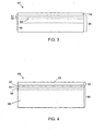
- FIG. 3 is a schematic cross-sectional view of a semiconductor-on-insulator structure having a pile-up region according to another embodiment of the present invention.
- FIG. 4 is a schematic cross-sectional view of a semiconductor-on-insulator structure according to another embodiment of the present invention.
- FIGS. 5-8 are schematic cross-sectional views of steps of a method for making a semiconductor-on-insulator structure according to one embodiment of the present invention.
- a semiconductor-on-insulator structure 20 includes a first layer 22, and a second layer 24.
- First layer 22 and second layer 24 are attached to one another either directly, as shown in FIG. 1 , or through one or more intermediate layers. If there are one or more intermediate layers intervening between first layer 22 and second layer 24, then first layer 22 and second layer 24 are desirably separated by no more than about 100 nm in distance.
- First layer 22 is formed from a substantially single-crystal semiconductor material
- second layer 24 is formed from a glass or a glass-ceramic.
- CTE coefficient of thermal expansion
- CTE(25-300 °C) The coefficient of thermal expansion (CTE) over the 25-300 °C temperature range (hereinafter CTE(25-300 °C)) of the glass or the glass ceramic is less positive than the CTE at 25 °C (hereinafter CTE(25 °C)) of the semiconductor material.
- the CTE(25-300 °C) of the glass or glass-ceramic can be positive, or can even be negative (e.g., for ⁇ -eucryptite-based glass-ceramics).
- CTE(25-300 °C) values are reported as an average CTE value over the temperature range.
- the CTE(25-300 °C) of the glass or glass-ceramic is at least 3x10 -7 /°C less positive than the CTE(25 °C) of the semiconductor material. More desirably, the CTE(25-300°C) of the glass or glass-ceramic is at least 5x10 -7 /°C less positive than the CTE(25 °C) of the semiconductor material. In certain desirable embodiments of the invention, the CTE(25-300 °C) of the glass or glass-ceramic is at least 7x10 -7 /°C less positive, or even 10x10 -7 /°C less positive than the CTE(25 °C) of the semiconductor material.
- the difference between the CTE(25 °C) of the semiconductor material and the CTE(25-300 °C) of the glass or glass-ceramic may be no greater than about 30x10 -7 /°C.
- the CTEs of the materials described herein are reported as the CTE of the homogeneous material itself, and not as the actual expansion behavior of the layers of materials in the actual semiconductor-on-insulator structures of the present invention. Since the first and second layers are attached to one another, and are generally rigid materials, their expansion and contraction behavior will be affected by the other layer(s) to which they are attached. If there is a difference in CTE between the materials of the first and second layer, and the layers are attached to one another at an elevated temperature T bond , one of the layers will experience tension and the other compression upon cooling to room temperature.
- the CTE(25-300 °C) of the glass or glass-ceramic is no more positive than about 22x 10 -7 /°C.
- the glass or glass-ceramic desirably has a CTE(25-300 °C) of no more positive than about 20x 10 -7 /°C, no more positive than 18x10 -7 /°C, or even no more positive than 15x10 -7 /°C.
- the glass or glass-ceramic has a strain point of less than 1050 °C.
- the semiconductor material is under tensile strain.
- the first layer is desirably under tensile strain at a use temperature of the semiconductor-on-insulator structure (e.g., 25°C, 100 °C, or over the 25-100 °C temperature range).
- Tensile strain can improve the electron and hole mobility properties of the semiconductor material, thereby allowing the construction of devices with improved properties.
- the first layer desirably has a bulk mobility that is at least about 105% of the bulk mobility of that of the semiconductor material in a substantially unstrained state.
- the first layer has a bulk mobility that is at least about 120% of the bulk mobility of that of the semiconductor material in a substantially unstrained state.
- Strained semiconductors are discussed in more detail in U.S. Patents 5,442,205 ; 6,107,653 ; 6,573,126 ; and 6,593,641 .
- the semiconductor material can be a silicon-based semiconductor material, or can be any other suitable type of semiconductor material, such as a III-V semiconductor, a II-IV semiconductor, a II-IV-V semiconductor, or a IV semiconductor.
- silicon-based semiconductor materials suitable for use as the semiconductor material of the first layer include silicon (e.g., undoped silicon, n-doped silicon, p-doped silicon); germanium-doped silicon (SiGe); and silicon carbide (SiC).
- Examples of other semiconductor materials which can be used in the first layer include Ge-, GeAs-, GaP-, and InP-based materials.
- the first layer can have virtually any suitable thickness.
- the first layer can be up to about 1 ⁇ m in thickness, and is desirably between about 10 nm and about 500 nm, with the thickness range of about 10 nm to about 150 nm being especially desirable.
- the semiconductor material of the first layer can have a wide range of CTEs depending on the material.
- the semiconductor material of the first layer can have a CTE(25 °C) between about 20x10 -7 /°C and about 70x10 -7 /°C.
- the semiconductor material of the first layer is in the form of a substantially single-crystal material.
- the word “substantially” is used in describing the first layer to take account of the fact that semiconductor materials normally contain at least some internal or surface defects either inherently or purposely added, such as lattice defects or a few grain boundaries.
- the word “substantially” also reflects the fact that certain dopants may distort or otherwise affect the crystal structure of the bulk semiconductor material.
- the glass or glass-ceramic of the second layer is desirably a silica-based glass or glass-ceramic.
- SiO 2 is present in the glass or glass-ceramic at a concentration of at least about 30 mol%. More desirably, SiO 2 is present in a concentration of at least about 40 mol%.
- Glass-ceramics suitable for use in the present invention can include any crystalline phase, such as mullite, cordierite, spinel, ⁇ -quartz, or ⁇ -spodumene. In certain desirable embodiments of the invention, the crystalline phase of the glass-ceramic of the second layer is spinel, ⁇ -quartz, or ⁇ -spodumene.
- the glass phase of the glass-ceramic is desirably sufficient to allow movement of positive ions away from the interface between the first and second layers during step (C) of the below-described method for making semiconductor-on-insulator structures.
- Non-silica-based glasses and glass-ceramics can be used in the practice of the invention, but are generally less desirable because of their higher cost and/or inferior performance characteristics.
- the glass or glass ceramic is desirably an oxide glass or oxide glass ceramic.
- second layers which are not oxide-based, e.g., non-oxide glasses may be desirable, but are generally of higher cost.
- the glass or glass-ceramic is desirably substantially transparent in the visible, near UV, and/or near IR wavelength ranges.
- the glass or glass-ceramic is desirably substantially transparent in the 350 nm to 2 ⁇ m wavelength range.
- the glass or glass-ceramic of the second layer can be produced from conventional raw materials using a variety of techniques familiar to the skilled artisan, and can be attached to the first layer using the methods described herein below, and in U.S. Patent Publication US 2004/0229444 entitled "GLASS-BASED SOI STRUCTURES".
- the glass or glass-ceramic desirably includes at least some positive ions which during step (C) of the method described herein below and in U.S. Patent Publication US 2004/0229444 move in the direction of the applied electric field, i.e., away from the interface between the bonded first and second layers and toward the back side of the second layer.
- Alkali ions e.g., Li + , Na + , and/or K + ions
- glasses and glass-ceramics having no alkali ions can be used in the present invention.
- glasses and glass-ceramics having other mobile ions such as alkaline-earth ions (e.g., Ca 2+ , Mg 2+ , Ba 2+ , Sr 2+ ) or other positive ions such as Ag + , Cu + , Zn2 + and various transition metal ions can be used in the second layer in the semiconductor-on-insulator structures of the present invention, although the latter set of ions may undesirably decrease optical transmission, especially in the UV.
- alkaline-earth ions e.g., Ca 2+ , Mg 2+ , Ba 2+ , Sr 2+
- other positive ions such as Ag + , Cu + , Zn2 +
- various transition metal ions can be used in the second layer in the semiconductor-on-insulator structures of the present invention, although the latter set of ions may undesirably decrease optical transmission, especially in the UV.
- the concentrations of alkali and alkaline-earth ions can vary over a wide range, representative concentrations being between 0.1 and 40 wt% on an oxide basis. Desirable alkali and alkaline-earth ion concentrations are 0.1-10 wt% on an oxide basis in the case of alkali ions, and 0-25 wt% on an oxide basis in the case of alkaline-earth ions. Many nominally alkali-free glasses have tens to hundreds of ppm of alkali contaminant, which can move during step (C) of the method described herein below.
- laminated structures can be used if desired.
- the layer of the laminate closest to the first layer should have the properties discussed herein for a second layer composed of a single glass or glass-ceramic material.
- Layers farther from the first layer preferably also have those properties, but may have relaxed properties because they do not directly interact with the first substrate. In the latter case, the second layer is considered to have ended when the properties specified for the second layer are no longer satisfied.
- first substrate and the second substrate can include surface layers over all or part of their external surfaces, e.g., an oxide layer on the semiconductor.
- oxide layer on the semiconductor substrate having a thickness greater than about 100 nm can lead to weak or no bonding with the glass or glass-ceramic substrate.
- intermediate layers between the first layer and the second layer they desirably have a combined thickness of less than about 100 nm. The combined thickness of any intermediate layers is more desirably less than about 50 nm, and even more desirably less than about 30 nm.
- an oxide layer having a greater thickness provides a high resistance to current flow and thus diminishes the electrolysis-type reaction at the interface between the first and second substrates which is believed to provide the desired strong bond in the methods described herein below. Accordingly, when an oxide layer is present on the bonding surface of the first substrate, it should function primarily as a passivation layer, as opposed to an insulating layer. Likewise, any oxide layer formed on the bonding surface of the second substrate should not interfere with current flow and thus will desirably have a thickness of less than about 100 nm. When surface layers are present on the bonding surfaces of the first and second substrates, they become intermediate layers between the first and second layers of the semiconductor-on-insulator structure.
- Desirable glass families for use as the glass in the present invention include aluminosilicate glasses, borosilicate glasses, aluminoborosilicate glasses, and rare earth aluminosilicate glasses.
- suitable low-expansion glass compositions are given below in mol% in Tables 1 and 2, below. The skilled artisan can make these and other suitable glass compositions using standard methods.
- the glasses listed below can be made by mixing the component oxide, halide (e.g., AlCl 3 ), phosphate (e.g., Al(PO 3 ) 3 or AlPO 4 ) and/or carbonate (CaCO 3 ) powders in a ball mill for 1 hour to make a 1 kg batch.
- the mixed batch can then be loaded into a Pt crucible and melted in a 1650 °C globar furnace overnight, after which time the melted glass can be poured onto a steel plate and annealed between 850 °C and 950 °C to alleviate stress.
- the properties of these glasses can be tailored by the skilled artisan by modifying the composition.
- the CTE can be increased by lowering the SiO 2 content or increasing the rare earth oxide content.
- alkali or alkaline-earth ions can be added small amounts (e.g., up to a few percent) alkali or alkaline-earth ions to the alkali and alkaline-earth ion-free compositions listed below in order to obtain glasses more suitable for use in the bonding methods described herein below.
- Another type of glass suitable for use as the second layer in the semiconductor-on-insulator structures of the present invention is an aluminum phosphorus silicate glass.
- Simple ternary compositions such as those of Examples 3A-3C in Table 3, below
- the expansion mismatch between the simple ternary compositions and the semiconductor material be too large (e.g., so large that they cause failure or delamination of the strained semiconductor layer)
- Typical modifying components include alkali and alkaline earth oxides (e.g., Na 2 O, Li 2 O, BaO, CaO), as well as ZnO, Y 2 O 3 , La 2 O 3 , Ga 2 O 3 , TiO 2 , ZrO 2 , HfO 2 , GeO 2 , SnO 2 Nb 2 O 5 and Ta 2 O 5 .
- Components such as BaO, Y 2 O 3 and La 2 O 3 are particularly desirable modifiers, as they result in an increase in the CTE without a large reduction in the strain point of the glass. Examples of modified glasses are shown as Examples 3D-N of Table 3, below.
- aluminum phosporus silicate glasses can be melted in Pt crucibles at 1650 °C using as raw materials a mixture of silica, alumina, aluminum metaphosphate (or orthophosphate) and any modifier as the appropriate oxide or carbonate. Glasses are typically annealed at about 900 °C.
- Glass-ceramic materials suitable for use in the present invention can be found in a number of composition families, including those based on crystals of spinel, ⁇ -quartz, and ⁇ -spodumene. Glass-ceramics suitable for use in the present invention may be based on other crystalline phases, such as mullite, cordierite, and ⁇ -eucryptite. Examples of such compositions are shown in Table 4, and are described in U.S. Patents 5,968,857 and 6,248,678 .
- glass-ceramic materials having low or even negative CTEs e.g., based on ⁇ -eucryptite or ⁇ -quartz, such as lithium aluminosilicate ⁇ -quartz glass-ceramics
- appropriate strain points may also be used in the present invention.
- Glass-ceramic materials having low expansion can be made using methods familiar to the skilled artisan. Although most glass-ceramics have some alkali or alkaline earth ions, any known low-expansion alkali- and alkaline-earth-free glass-ceramics can be modified with a small amount of alkali or alkaline-earth ions in order to provide glass-ceramic materials more suitable for use in the bonding methods described herein below.
- Example 4A Example 4B
- Example 4C Example 4D
- Example 4E SiO 2 71.6 68.8 68.8 68.8 70.7 Al 2 O 3 12.7 19.2 19.2 19.2 22.1 ZnO 4.4 1.0 1.0 1.0 0 MgO 2.1 1.8 1.8 1.8 0 BaO 1.2 0.8 0.8 0.8 0 Li 2 O 0 2.7 2.7 2.7 4.0 Na 2 O 0 0 0 0 2.0 K 2 O 0 0 0 0 1.2 TiO 2 5.0 2.7 2.7 2.7 2.8 ZrO 2 3.0 1.8 1.8 1.8 1.6
- the tensile strain of the first layer at a given use temperature will depend strongly upon the difference in the temperature between the bonding temperature and the use temperature, as well as on the relative CTEs as a function of temperature of the materials of the first layer and the second layer.
- the bonding temperature is the temperature of the interface at which the first layer and the second layer become attached to one another.
- the bonding temperature will be between T 1 and T 2 , and may be approximated as the average of T 1 and T 2 , or may be determined by thermal modeling or measurement as would be apparent to the skilled artisan.
- the first layer In order to put the first layer under strain at the use temperature, the first layer must seek to contract more as a result of cooling from the bonding temperature T bond to the use temperature.
- the CTEs of the materials of the first layer and of the second layer are such that ⁇ T use T bond CT ⁇ E first layer T - CT ⁇ E second layer T ⁇ dT is greater than zero.
- ⁇ T use T bond CT ⁇ E first layer T - CT ⁇ E second layer T ⁇ dT is greater than about 1x10 -4 .
- ⁇ T use T bond CT ⁇ E first layer T - CT ⁇ E second layer T ⁇ dT is greater than about 2x10 -4 .
- ⁇ T use T bond CT ⁇ E first layer T - CT ⁇ E second layer T is greater than about 5x10 -4 .
- the semiconductor-on-insulator structure has the above-recited values of ⁇ T use T bond CT ⁇ E first layer T - CT ⁇ E second layer T ⁇ dT over a use temperature range of 25-100 °C.
- a semiconductor-on-insulator structure has the above-recited values of ⁇ T use T bond CT ⁇ E first layer T - CT ⁇ E second layer T ⁇ dT at a use temperature T use of 25 °C.
- a semiconductor-on-insulator structure has the above-recited values of ⁇ T use T bond CT ⁇ E first layer T - CT ⁇ E second layer T ⁇ dT at a use temperature of 100 °C.
- the strength of the bond between the glass or glass ceramic and the semiconductor layer attached thereto is a key property of a semiconductor-on-insulator structure. High bond strength and durability are very important to ensure that the semiconductor-on-insulator structure can withstand the processing associated with the manufacture of thin film transistors and other devices within or on the structure.
- the bond strength between the first layer and the second layer is desirably at least 8 J/m 2 . More desirably, the bond strength between the first layer and the second layer is at least 10 J/m 2 . In certain especially desirable embodiments of the invention, the bond strength between the first layer and the second layer is at least 15 J/m 2 .
- Bond energies can be determined using indentation measurements, which can be performed using a Nano Indenter II (MTS Systems Corporation, Eden Prairie, MN) equipped with a Berkovich diamond indenter. As the skilled artisan will appreciate, other equipment can be used to perform indentation measurements. Indentations are to be made covering a range of loads, and the region immediately surrounding the indentation is to be examined for evidence of delamination. Calculation of bond energy is made in accordance with D.B. Marshall and A.G. Evans, "Measurement of Adherence of Residually Stressed Films by Indentation. I. Mechanics of Interface Delamination", J. Appl. Phys, 56[10] 2632-2638 (1984 ). Further details of the bond energy determination can be found in U.S. Publication US 2004-0229444 .
- a semiconductor-on-insulator structure 40 includes a first layer 42 and a second layer 44, substantially as described above for the embodiment of FIG. 1 .
- the second layer 44 has a first face 46, and a second face 48 separated by a distance D 2 , the first face 46 being substantially parallel to the second face, and closer to the first layer 42 than the second face 48.
- the faces are described as being “substantially parallel” in order to account for the fact that there might be some slight angle (e.g., up to a few degrees) between them.
- the phrase "substantially parallel” also includes the possibility that one or more of the faces may not be completely flat.
- the second layer 44 also includes a reference surface 50, which is within the second layer 44, is substantially parallel to the first face 46, and is separated from the first face 46 by a distance D 2 /2.
- the second layer 44 includes positive ions of one or more types, each type of positive ion having a reference concentration C i/Ref at the reference surface 50.
- the second layer also has a positive ion depletion region 52, which begins at the first face and extends toward the reference surface, in which the concentration of at least one type of positive ion is depleted relative to the reference concentration C i/Ref .
- the depleted ion may be a mobile positive ion, for example, an alkali ion or an alkaline-earth ion.
- the positive ion depletion region can be formed in the methods described herein below and in U.S. Patent Publication US 2004-0229444 by the motion of the positive ions during step (C).
- the positive ion depletion region 52 of a semiconductor-on-insulator structure 60 (substantially as described above with respect to FIG. 2 ) has a distal edge 62.
- the second layer 44 further includes a pile-up region 54 in the vicinity of the distal edge 62. In the pile-up region 54, the concentration of at least one type of positive ion is enhanced relative to C i/Ref for that ion.
- the enhanced ion may be, for example, a mobile ion such as an alkali ion or an alkaline-earth ion, and is desirably the same as the depleted ion of the positive ion depletion region 52.
- the pile-up region can be formed in the methods described herein below and in U.S. Patent Publication US 2004-0229444 by the motion of the positive ions during step (C).
- Semiconductor-on-insulator structure 80 includes a first layer 82 and a second layer 84, substantially described above.
- Semiconductor-on-insulator structure 80 includes, in order, the semiconductor material (90); the semiconductor material with an enhanced oxygen content (92); the glass or glass-ceramic with a reduced positive ion concentration for at least one type of positive ion (94); the glass or glass-ceramic material with an enhanced positive ion concentration for at least one type of positive ion (96); and the glass or glass ceramic (98).
- Such a structure can be made using the methods described herein below and in U.S. Patent Publication US 2004-0229444 .
- the glass or glass-ceramic of the second layer has a relatively low concentration of alkali ions.
- the sum of the concentrations of lithium, sodium and potassium ions in the glass or glass-ceramic on an oxide basis is less than about 2 wt%. More desirably, the sum of the concentrations of lithium, sodium and potassium ions in the glass or glass-ceramic on an oxide basis is less than about 1 wt%. In certain especially desirable embodiments of the present invention, the sum of the concentrations of lithium, sodium and potassium ions in the glass or glass-ceramic on an oxide basis is less than about 0.1 wt%.
- a semiconductor-on-insulator structure as described herein has a maximum dimension no less than 10 cm.
- the semiconductor-on-insulator structures of the present invention can be made with virtually any desirable layer thicknesses.
- the first layer desirably has a thickness less than about 10 ⁇ m. More desirably, the first layer desirably has a thickness less than about 1 ⁇ m. In certain desirable embodiments of the invention, the first layer has a thickness between about 10 nm and 500 nm.
- the second layer desirably has a thickness between about 0.1 mm and about 10 mm. More desirably, the second layer has a thickness between about 0.5 mm and about 1 mm.
- insulating layers having a thickness greater than or equal to 1 ⁇ m are desirable, e.g., to avoid parasitic capacitive effects which arise when standard semiconductor-on-insulator structures having a silicon/SiO 2 /silicon configuration are operated at high frequencies. In the past, such thicknesses have been difficult to achieve.
- a semiconductor-on-insulator structure having an insulating layer thicker than 1 ⁇ m is readily achieved by simply using a second layer whose thickness is no less than 1 ⁇ m. A preferred lower limit on the thickness of the second substrate is thus 1 ⁇ m.
- the second layer needs to be thick enough to support the first layer through the process steps of the invention, as well as subsequent processing performed on the SOI structure.
- a thickness beyond that needed for the support function or that desired for the ultimate SOI structure is generally not preferred since the greater the thickness of the second substrate, the lower the electric field strength within the substrate during step (C) of the method of the present invention for the same applied voltage difference.
- a thin film transistor includes a patterned element including the semiconductor-on-insulator structure as described above.
- a liquid crystal display includes a liquid crystalline material and a patterned element including a semiconductor-on-insulator structure as described hereinabove, desirably having a substantially transparent second layer.
- an OLED device includes a light-emitting organic material and a patterned element including a semiconductor-on-insulator structure as described hereinabove desirably having a substantially transparent second layer. As described in U.S. Patent Publication US 2004-0229444 , the skilled artisan can use conventional methods to make these devices.
- step (A) of the method illustrated in FIG. 5 , first and second substrates (110, 120) are provided, wherein:
- step (B) of the method shown in FIG. 6 , the first and second bonding surfaces (111, 121) are brought into contact (once brought into contact, the first and second bonding surfaces form what is referred to herein as the "interface" between the first and second substrates).
- step (C) of the method shown in FIG. 7 , for a period of time sufficient for the first and second substrates to bond to one another at the first and second bonding surfaces (i.e., at the interface), the following steps are substantially simultaneously performed:
- step (D) of the method shown in FIG. 8 , the bonded first and second substrates (110, 120) are cooled to a common temperature (e.g., to a common temperature such as room temperature); and the first and second parts (114, 115) are separated at the separation zone (113a-b), thereby forming semiconductor-on-insulator structure 140 having a first layer 142 (arising from the first substrate 110) and a second layer 144 (arising from the second substrate 120).
- a common temperature e.g., to a common temperature such as room temperature
- the first and second parts (114, 115) are separated at the separation zone (113a-b), thereby forming semiconductor-on-insulator structure 140 having a first layer 142 (arising from the first substrate 110) and a second layer 144 (arising from the second substrate 120).
- the CTE of the glass or glass-ceramic and the CTE of the are desirably chosen such that the semiconductor material is under tensile strain at a use temperature.
- the semiconductor material is desirably under tensile strain at 25 °C, at 100 °C, or over the temperature range from 25-100°C.
- the properties of the materials (CTE and otherwise) of the first and second substrates are desirably substantially as described hereinabove for the semiconductor-on-insulator structures of the present invention.
- the CTE(25-300 °C) of the glass or glass-ceramic is less positive than the CTE(25 °C) of the semiconductor material.
- the CTEs of the materials of the first layer and of the second layer are such that ⁇ T use T bond CT ⁇ E first layer T - CT ⁇ E second layer T ⁇ dT is greater than zero for use temperatures of, for example, 25 °C, 100°C, or the 25-100 °C temperature range.
- the glass or glass-ceramic desirably has one or both of the following sets of characteristics:
- non-bridging oxygens in a glass or in the glass phase of a glass-ceramic are those oxygens contributed to the glass by non-network forming components of the glass.
- the non-bridging oxygens include those oxygens which are part of the glass through the incorporation of alkaline-earth oxides (e.g., MgO, CaO, SrO, and/or BaO) in the glass composition.
- step (C) an electrolysis-type reaction takes place during step (C).
- the semiconductor substrate serves as the positive electrode for the electrolysis-type reaction and that reactive oxygen is produced in the region of the interface between the first and second substrates.
- This oxygen is believed to react with the semiconductor material (e.g., silicon) forming, in situ, a hybrid region (116) of oxidized semiconductor (e.g., a silicon oxide region for a silicon-based semiconductor).
- This hybrid region begins at the interface and extends into the first substrate.
- the presence of non-bridging oxygens in the glass or glass-ceramic of the second substrate is believed to play a role in the generation of the oxygens that react with the semiconductor material of the first substrate.
- the second substrate to be a material which can be manufactured in large quantities at low cost. That is, by eliminating high temperature processing, the invention eliminates the need for a support substrate composed of an expensive high temperature material, such as, silicon, quartz, diamond, sapphire, etc.
- the ability to achieve a strong bond without the need for a high temperature treatment allows the second substrate to be composed of a glass or a glass-ceramic; in one embodiment the glass or glass-ceramic exhibits a strain point less than 1000 °C. More particularly, for display applications, the glass or glass-ceramic typically has a strain point less than 800 °C, and in further embodiments less than 700 °C. For electronics and other applications, the strain point is preferably less than 1000 °C. As well known in the glass making art, glasses and glass-ceramics having lower strain points are easier to manufacture than glasses and glass-ceramics having higher strain points.
- the glass or glass-ceramic should be able to conduct electricity at least to some extent.
- the conductivity of glasses and glass-ceramics depends on their temperature and thus in achieving a strong bond between the semiconductor material and the glass or glass-ceramic, there is a balance among: 1) the conductivity of the glass or glass-ceramic, 2) the temperatures (T 1 and T 2 ) used in step (C), 3) the strength of the electric field applied to the first and second substrates during step (C), and 4) the amount of time during which step (C) is performed.
- the glass or glass-ceramic preferably has a resistivity p at 250 °C that is less than or equal to 10 16 ⁇ -cm (i.e., a conductivity at 250 °C that is greater than or equal to 10 -16 Siemens/cm). More preferably, ⁇ at 250 °C is less than or equal to 10 13 ⁇ -cm, and most preferably, it is less than or equal to 10 11.5 ⁇ -cm.
- quartz has the requisite resistivity at 250 °C of 10 11.8 ⁇ -cm, it lacks positive ions that can move during step (C), and it thus follows that quartz is unsuitable for use as the second substrate in producing semiconductor-on-insulator structures in accordance with the above procedures.
- pretreatment of the bonding surface 111 of first substrate 110 to reduce its hydrogen concentration has been found advantageous in achieving bonding of the second part 115 of the first substrate to second substrate 120.
- a reduction in hydrogen concentration has been found to be of particular importance when transferring silicon films from silicon wafers implanted with hydrogen ions to glass substrates containing alkaline-earth ions. It is believed that a reduction in hydrogen concentration will also be advantageous for glass and glass ceramics having high strain points, e.g., in the 850 °C to 900°C range, which are expected to be needed for RF applications in wireless and other electronics applications.
- the surface of an implanted silicon wafer has a high hydrogen concentration, e.g., a high hydrogen ion concentration.
- the hydrogen termination at the Si surface inhibits the bonding process and thus it has been found desirable to reduce the hydrogen concentration on the implanted Si wafer surface by using a gentle oxidizing treatment in order to obtain effective Si layer transfer to glass wafers of the foregoing types.
- Reduction in hydrogen concentration results in making the implanted silicon wafer more hydrophilic and allows the bonding to take place during the application of voltage and heat. The strong bond formed during the process allows uniform separation of the Si film from the mother wafer.
- Various approaches can be used to reduce the hydrogen concentration on the surface of an implanted wafer.
- Preferred approaches involve a mild oxidation treatment of the surface, such as, treatment of the wafer with an oxygen plasma, treatment with hydrogen peroxide, hydrogen peroxide and ammonia, hydrogen peroxide and ammonia followed by hydrogen peroxide and an acid, or combinations of these processes.
- Treatment with an oxygen plasma is the preferred approach, especially in a commercial setting.
- hydrogen terminated surface groups oxidize to hydroxyl groups, which in turn makes the surface of the silicon wafer hydrophilic.
- the treatment is preferably carried out at room temperature for the oxygen plasma and at a temperature between 25-100 °C for the ammonia + peroxide or ammonia + peroxide followed by acid + peroxide treatments.
- FIG. 6 this figure illustrates step (B) of the process of the invention in which the first and second substrates 110 and 120 are brought into contact at their bonding surfaces 111 and 121.
- the first and second substrates are heated prior to step (B), e.g., are heated so that force-applying surfaces 112 and 122 are at T 1 and T 2 , respectively. In this way, differential expansion between the first and second substrates is avoided during the bonding process of step (C).
- the first and second substrates are not pre-heated prior to step (B), but are heated after bonding surfaces 111 and 121 have been brought into contact and before the beginning of step (C) and/or during the initial part of step (C) before substantial bonding has occurred.
- the bonding surfaces can be separated by spacers which are removed once the desired temperatures of the first and second substrates have been reached.
- the processing chamber which is shown schematically at 140 in FIG. 7 , can have a variety of configurations.
- a bonder of the type sold by SÜSS MICROTEC of Munich, Germany can be used as the processing chamber.
- the same equipment can be used for commercial applications, although equipment capable of simultaneously processing multiple first substrate/second substrate assemblies will generally be preferred.
- the invention uses low to moderate temperatures, pressures, electric field strengths, and vacuum levels, the requirements which the processing chamber needs to satisfy are not demanding, which is another important advantage of the invention, i.e., the invention can be practiced with equipment which is both relatively inexpensive and widely available or easily fabricated for custom applications.
- FIG. 7 shows the central step of the process, i.e., step (C), where the first and second substrates are bonded to one another.
- Step (C) is performed for a period of time sufficient for the first and second substrates to bond to one another at the first and second bonding surfaces.
- step (C) can be performed for a period between 45 and 90 minutes. Shorter periods of time are, of course, generally preferred (e.g., times less than 30 minutes) and in a commercial setting, it is expected that the time required to perform step (C) can be reduced to a period of 5-15 minutes or less through the optimization of substrate materials, processing temperatures, and applied voltages.
- Step (C) is preferably performed under moderate vacuum conditions, i.e., chamber 40 is evacuated while step (C) is performed.
- the pressure in the chamber is less than or equal to 1 millibar, and most preferably, less than or equal to 10 -3 millibars.
- step (C) can be performed in an inert atmosphere, such as, an atmosphere of argon, helium, or the like.
- first and second substrates For any particular set of first and second substrates, persons skilled in the art will readily be able to determine suitable combinations of time, temperature, and field strength for step (C) from the present disclosure. In particular, such persons will be able to select combinations of these parameters which create a bond between the semiconductor and the glass or glass-ceramic which is strong enough for the semiconductor-on-insulator structure to withstand the various forces and environmental conditions to which it will be exposed during further processing and/or use.
- the voltages V 1 and V 2 desirably satisfy the relationship: 100 V/cm ⁇ (V 1 -V 2 )/D ⁇ 40 kV/cm, where D is the sum of the thicknesses of the first substrate and the second substrate.
- the electric field applied in step (C) also moves positive ions (cations) within the second substrate in a direction from the second substrate's bonding surface (the second bonding surface) towards its force-applying surface (the second force-applying surface).
- Such movement preferably forms a positive ion depletion region (123) which begins at the interface between the first and second substrates and extends into the second substrate, i.e., the positive ion depletion region begins at the second bonding surface and extends into the second substrate towards the second force-applying surface.
- Such a positive ion depletion region is especially desirable when the glass or glass-ceramic contains alkali ions, e.g., Li + , Na + , and/or K + ions, since such ions are known to interfere with the operation of semiconductor devices.
- alkali ions e.g., Li + , Na + , and/or K + ions
- Alkaline-earth ions e.g., Mg 2+ , Ca 2+ , Sr 2+ , and/or Ba 2+ , can also interfere with the operation of semiconductor devices and thus the positive ion depletion region also preferably has reduced concentrations of these ions.
- the positive ion depletion region once formed is stable over time even if the semiconductor-on-insulator structure is heated to an elevated temperature comparable to, or even to some extent higher than, that used in step (C). Having been formed at an elevated temperature, the positive ion depletion region is especially stable at the normal operating and formation temperatures of semiconductor-on-insulator structures. These considerations ensure that alkali and alkaline-earth ions will not diffuse back from the glass or glass-ceramic into the semiconductor of the semiconductor-on-insulator structure during use or further device processing, which is an important benefit derived from using an electric field as part of the bonding process of step (C).
- the operating parameters needed to achieve a positive ion depletion region of a desired width and a desired reduced positive ion concentration for all of the positive ions of concern can be readily determined by persons skilled in the art from the present disclosure.
- the positive ion depletion region is a characteristic feature of an semiconductor-on-insulator structure produced in accordance with the method aspects of the present invention.
- the application of the electric field can also create "pile-up" regions for one or more of the mobile positive ions contained in the glass or glass-ceramic. When present, such regions are located at or near the side (edge) of the depletion region farthest from the interface between the first and second substrates.
- the positive ion has a concentration above its bulk concentration. For example, when measured in atomic percent, the peak concentration of the positive ion in the pile-up region can be, for example, up to 5 times greater than the bulk concentration.
- such a pile-up region when present, is a characteristic feature of an semiconductor-on-insulator structure produced in accordance with the method aspects of the present invention.
- the temperatures of the first and second substrates during step (C), i.e., the values of T 1 and T 2 , are chosen to perform the important function of weakening (e.g., fracturing) the semiconductor substrate (first substrate) at the separation zone so that the first substrate can be divided into first and second parts, the second part being bonded to the second substrate.
- the weakening of the semiconductor substrate at the separation zone primarily occurs as the bonded first and second substrates are cooled after step (C), e.g., to room temperature.
- step (C) e.g., to room temperature.
- T 1 and T 2 this cooling causes the first and second substrates to differentially contract.
- This differential contraction applies stress to the first substrate which manifests itself as a weakening/fracturing of the first substrate at the separation zone.
- the differential contraction is such that the first substrate seeks to contract more than the second substrate.
- T 1 and T 2 used during step (C) will depend on the relative coefficients of thermal expansion of the first and second substrates, the goal in choosing these values being to ensure that one of the substrates, preferably, the first substrate, seeks to contract to a greater extent than the other substrate, preferably, the second substrate, so as to apply stress to, and thus weaken, the separation zone during cooling.
- any particular application of the invention e.g., any particular semiconductor material and any particular glass or glass-ceramic
- persons skilled in the art will readily be able to select values for T 1 and T 2 based on the present disclosure which will provide a level of differential contraction sufficient to weaken the separation zone so that the first and second parts of the first substrate can be separated from one another to produce the desired SOI structure.
- T 1 , T 2 and the strain point T 5 of the glass or glass ceramic satisfy the relationships: T s - 350 ⁇ °C ⁇ T 1 ⁇ T s + 350 ⁇ °C ; and T s - 350 ⁇ °C ⁇ T 2 ⁇ T s + 350 ⁇ °C .
- both T 1 and T 2 are between 300 °C and 1000 °C. In certain desirable embodiments of the invention, both T 1 and T 2 are between 300 °C and 800 °C.
- separation of the first and second parts at the separation zone results in each part having an "exfoliation" surface where the separation occurred.
- an exfoliation surface upon initial formation, i.e., before any subsequent surface treatments, such an exfoliation surface is characterized by a surface roughness which is generally at least on the order of 0.5 nanometers RMS, e.g., in the range of 1-100 nanometers, and depending on the process conditions used, will typically have a concentration of the implanted ion used to form the separation zone, e.g., hydrogen, above that present in the body of the first or second parts.
- the exfoliation surface as initially formed will also be characterized by a distorted crystal structure as seen by TEM.
- the exfoliation surface is polished prior to use so that its RMS surface roughness is reduced to 1 nanometer or less, e.g., to a RMS surface roughness on the order of 0.1 nanometers for electronic applications.
- the phrase "exfoliation surface” includes the surface as initially formed and the surface after any subsequent treatments.
- Separation zone 113 is formed using implantation/exfoliation techniques of the type currently known to those skilled in the art or which may be developed in the future.
- the separation zone is preferably formed using the hydrogen ion implantation techniques of the references discussed above.
- Other currently-known techniques can also be used to form the separation zone, such as, co-implantation of hydrogen and helium ions or hydrogen and boron ions.
- the first substrate needs to be separable into the first and second parts at the separation zone during step (D).
- the separation zone needs to respond to the heat treatment/cooling process by becoming weaker so that the division of the first substrate into the first and second parts can occur.
- step (C) The pressure applied to the first and second substrates during step (C) ensures that those substrates are in intimate contact while undergoing the heat and electric field treatments of that step. In this way, strong bonding between the substrates can be achieved.
- the semiconductor substrate (the first substrate) will be able to withstand higher levels of applied pressure than the glass or glass-ceramic substrate (the second substrate).
- the pressure is chosen to provide intimate contact between the substrates without damaging the second substrate.
- the force per unit area P applied to the first and second force-applying surfaces of the first and second substrates, respectively, preferably satisfies the relationship: 1 psi ⁇ P ⁇ 100 psi ; and most preferably, the relationship: 1 psi ⁇ P ⁇ 50 psi .
- the invention can be practiced using a single first substrate and a single second substrate.
- the methods of the invention can be used to form more than one SOI structure on a single second substrate.
- steps (A) through (D) can be used to form a first SOI structure which does not cover the entire area of the second substrate. Thereafter, steps (A) through (D) can be repeated to form a second SOI structure which covers all or part of the area not covered by the first SOI structure.
- the second SOI structure may be the same or different from the first SOI structure, e.g., the second SOI structure can be made using a first substrate composed of a substantially single-crystal semiconductor material that is the same or different from the semiconductor material of the first substrate used in producing the first SOI structure.
- multiple SOI structures are formed simultaneously on a single second substrate by providing multiple (i.e., two or more) first substrates in step (A), bringing all of those first substrates into contact with a single second substrate in step (B), and then performing steps (C) and (D) on the resulting multiple first substrate/single second substrate assembly.
- the multiple first substrates provided in step (A) can all be the same, all different, or some the same and some different.
- the resulting multiple SOI structures on a single glass or glass-ceramic substrate can be contiguous or separated as appropriate for the particular application of the invention. If desired, gaps between some or all of the adjacent structures can be filled with, for example, semiconductor material to obtain one or more continuous semiconductor layers on a glass or glass-ceramic substrate of any desired size.
- a 100 mm diameter, 1 mm thick wafer of glass 3N of Table 3 was polished to smoothness.
- a silicon wafer 525 ⁇ m in thickness was implanted with hydrogen at 100 keV and an ion dosage of 8x10 16 ions/cm 2 was cleaned with detergent and distilled water followed by a 10% nitric acid wash, and brought into contact with the glass wafer in a SUSS MICROTEC bonder.
- the glass wafer was heated at 450 °C and the silicon wafer at 400 °C in vacuum, and 10 psi pressure and 1750 V potential difference (glass at ground, silicon wafer at 1750 V) was applied for five minutes.
- the glass wafer was heated at 575°C and the silicon wafer at 525 °C for ten minutes, after which time the potential difference and pressure were removed, and the bonded wafers allowed to cool down.
- the cooled wafers separated into a silicon-on-glass wafer with a thin silicon layer, and a silicon wafer.
- the silicon layer on the glass had a thin, damaged top layer, and an undamaged single-crystal silicon bottom layer.
- the thin damaged layer can be polished or etched off to obtain the desired silicon-on-glass wafer.
Abstract
Claims (13)
- Structure de semi-conducteur sur isolant comprenant :une première couche; etune seconde couche qui est fixée sur la première couche directement ou par l'intermédiaire d'une ou de plusieurs couches intermédiaires, dans laquelle:dans laquelle le coefficient de dilatation thermique CTE (25°C - 300 °C) du verre ou du verre - céramique est inférieur au CTE (25°C) du matériau semi-conducteur.la première couche comprend un matériau semi-conducteur sensiblement monocristallin ;la seconde couche comprend du verre ou du verre - céramique, comprenant :(i) des première et seconde faces sensiblement parallèles séparées par une distance D2, la première face étant plus proche de la première couche que la seconde face;(ii) une surface de référence qui : 1) se situe à l'intérieur de la seconde couche; 2) est sensiblement parallèle à la première face; et 3) est séparée de cette face par une distance égale à D2/2;(iii) des ions positifs d'un ou de plusieurs types, chaque type d'ion positif présentant une concentration de référence Ci/Ref au niveau de la surface de référence; et(iv) une région, la région d'appauvrissement en ions positifs, qui commence au niveau de la première face et qui s'étend vers la surface de référence dans laquelle la concentration d'un type au moins en ions positifs est appauvrie par rapport à la concentration de référence Ci/Ref de cet ion ; et
- Structure de semi-conducteur sur isolant selon la revendication 1, dans laquelle la première couche subit une tension de traction à 25 °C.
- Structure de semi-conducteur sur isolant selon la revendication 1, dans laquelle la première couche présente une mobilité de masse qui est au moins égale à 105 % environ de la mobilité de masse du matériau semi-conducteur dans un état sensiblement non étiré.
- Structure de semi-conducteur sur isolant selon la revendication 1, dans laquelle le verre ou le verre-céramique présente un point de trempe inférieur à 1050°C.
- Structure de semi-conducteur sur isolant selon la revendication 1, dans laquelle le matériau semi-conducteur est un matériau semi-conducteur à base de silicium.
- Structure de semi-conducteur sur isolant selon la revendication 1, dans laquelle le verre ou le verre - céramique présente un CTE (25°C - 300 °C) qui n'est pas plus positif que 22 × 10-7/°C environ.
- Structure de semi-conducteur sur isolant selon la revendication 1, dans laquelle la différence entre le CTE (25 °C) du matériau semi-conducteur et le CTE (25°C - 300 °C) du verre ou du verre - céramique n'est pas supérieur à 30 × 10-7/°C environ.
- Structure de semi-conducteur sur isolant selon la revendication 1, dans laquelle l'expression suivante:

est supérieure à zéro;
dans laquelle Tbond est la température à laquelle la première couche a été liée à la seconde couche, et dans laquelle Tuse est la température d'utilisation de la structure de semi-conducteur sur isolant. - Structure de semi-conducteur sur isolant selon la revendication 1, dans laquelle la force de liaison entre les première et seconde couches est au moins égale à 8 J / m2.
- Structure de semi-conducteur sur isolant selon la revendication 1, dans laquelle la première couche présente une épaisseur qui n'est pas supérieure à 10 µm environ.
- Procédé de production d'une structure de semi-conducteur sur isolant qui comprend les étapes consistant à :(A) fournir des premier et second substrats dans lequel:(1) le premier substrat comprend une première surface extérieure destinée à une liaison avec le second substrat (la première surface de liaison), une seconde surface extérieure destinée à appliquer une force sur le premier substrat (la première surface d'application de force), et une zone intérieure destinée à séparer le premier substrat en une première partie et en une seconde partie (la zone de séparation), dans lequel :(a) la première surface de liaison, la première surface d'application de force, et la zone de séparation sont sensiblement parallèles les unes aux autres;(b) la seconde partie se situe entre la zone de séparation et la première surface de liaison ; et(c) le premier substrat comprend un matériau semi-conducteur sensiblement monocristallin; et(2) le second substrat comprend deux surfaces extérieures, une destinée à une liaison sur le premier substrat (la seconde surface de liaison) et une autre destinée à appliquer une force sur le second substrat (la seconde surface d'application de force), dans lequel :(a) la seconde surface de liaison et la seconde surface d'application de force sont sensiblement parallèles l'une à l'autre et sont séparées l'une de l'autre par une distance D2; et(b) le second substrat comprendre du verre ou du verre - céramique;(B) mettre en contact les première et seconde surfaces de liaison ;(C) pendant une période de temps suffisante pour que les premier et second substrats se lient l'un à l'autre au niveau des première et seconde surfaces de liaison, exécuter simultanément les étapes suivantes :(1) appliquer une force sur les première et seconde surfaces d'application de force de façon à presser ensemble les première et seconde surfaces de liaison ;(2) soumettre les premier et second substrats à un champ électrique qui est caractérisé par des première et seconde tensions V1 et V2 au niveau des première et seconde surfaces d'application de force, respectivement, lesdites tensions étant uniformes au niveau de ces surfaces, V1 étant supérieure à V2 de telle sorte que le champ électrique soit dirigé à partir du premier substrat vers le second substrat ; et(3) chauffer les premier et second substrats, ledit chauffage étant caractérisé par des première et seconde températures T1 et T2 au niveau des première et seconde surfaces d'application de force, respectivement, lesdites températures étant uniformes au niveau de ces surfaces et étant sélectionnées de telle sorte que lors d'un refroidissement à une température commune, les premier et second substrats subissent une contraction différentielle de façon affaiblir de ce fait le premier substrat au niveau de la zone de séparation ; et(D) refroidir les premier et second substrats liés et séparer les première et seconde parties au niveau de la zone de separation ;dans lequel T1, T2, le coefficient de dilatation thermique CTE du matériau semi-conducteur et le CTE du matériau de verre ou de verre - céramique sont sélectionnés de telle sorte que le matériau semi-conducteur subisse une tension de traction à 25 °C.
- Procédé selon la revendication 11, dans lequel le coefficient de dilatation thermique CTE (25 °C - 300 °C) du verre ou du verre - céramique est moins positif que le CTE (25 °C) du matériau semi-conducteur.
- Procédé selon la revendication 11, dans lequel l'expression suivante :

est supérieure à zéro ;
dans laquelle Tbond est la température à laquelle la première couche a été collée sur la seconde couche, et dans laquelle Tuse est la température d'utilisation de la structure de semi-conducteur sur isolant.
Applications Claiming Priority (2)
| Application Number | Priority Date | Filing Date | Title |
|---|---|---|---|
| US60278204P | 2004-08-18 | 2004-08-18 | |
| PCT/US2005/027786 WO2006023289A2 (fr) | 2004-08-18 | 2005-08-03 | Structures contraintes semi-conducteur-sur-isolant et methodes pour fabriquer ces structures |
Publications (3)
| Publication Number | Publication Date |
|---|---|
| EP1782472A2 EP1782472A2 (fr) | 2007-05-09 |
| EP1782472A4 EP1782472A4 (fr) | 2009-08-12 |
| EP1782472B1 true EP1782472B1 (fr) | 2011-10-05 |
Family
ID=35968055
Family Applications (1)
| Application Number | Title | Priority Date | Filing Date |
|---|---|---|---|
| EP05779271A Expired - Fee Related EP1782472B1 (fr) | 2004-08-18 | 2005-08-03 | Structures contraintes semi-conducteur-sur-isolant et methodes pour fabriquer ces structures |
Country Status (7)
| Country | Link |
|---|---|
| US (1) | US7262466B2 (fr) |
| EP (1) | EP1782472B1 (fr) |
| JP (1) | JP2008510315A (fr) |
| KR (1) | KR101140450B1 (fr) |
| CN (1) | CN100527416C (fr) |
| TW (1) | TWI289904B (fr) |
| WO (1) | WO2006023289A2 (fr) |
Families Citing this family (24)
| Publication number | Priority date | Publication date | Assignee | Title |
|---|---|---|---|---|
| DE10350034A1 (de) * | 2003-10-27 | 2005-05-25 | Robert Bosch Gmbh | Antennenanordnung insbesondere für Radaranwendungen bei Kraftfahrzeugen |
| US7473969B2 (en) * | 2004-08-18 | 2009-01-06 | Corning Incorporated | High strain glass/glass-ceramic containing semiconductor-on-insulator structures |
| CN101243018B (zh) * | 2005-08-17 | 2013-01-23 | 康宁股份有限公司 | 高应变点玻璃 |
| JP5041714B2 (ja) * | 2006-03-13 | 2012-10-03 | 信越化学工業株式会社 | マイクロチップ及びマイクロチップ製造用soi基板 |
| US7608521B2 (en) * | 2006-05-31 | 2009-10-27 | Corning Incorporated | Producing SOI structure using high-purity ion shower |
| US20070281440A1 (en) * | 2006-05-31 | 2007-12-06 | Jeffrey Scott Cites | Producing SOI structure using ion shower |
| KR100851551B1 (ko) * | 2007-03-12 | 2008-08-11 | 삼성전자주식회사 | 반도체 장치 및 그 형성 방법 |
| WO2008121262A2 (fr) * | 2007-03-30 | 2008-10-09 | Corning Incorporated | Structures semi-conducteur sur isolateur à base de verre-céramique et leur procédé de fabrication |
| US20090032873A1 (en) * | 2007-07-30 | 2009-02-05 | Jeffrey Scott Cites | Ultra thin single crystalline semiconductor TFT and process for making same |
| KR101479804B1 (ko) * | 2007-09-13 | 2015-01-06 | 아사히 가라스 가부시키가이샤 | TiO2 함유 석영 유리 기판 |
| KR101568897B1 (ko) * | 2008-09-26 | 2015-11-12 | 코닝 인코포레이티드 | 유리 세라믹계 반도체-온-절연체 구조 및 그 제조방법 |
| FR2942910B1 (fr) * | 2009-03-06 | 2011-09-30 | Soitec Silicon On Insulator | Procede de fabrication d'une heterostructure visant a reduire l'etat de contrainte en tension du substrat donneur |
| US8062956B2 (en) | 2009-08-26 | 2011-11-22 | Corning Incorporated | Semiconductor on insulator and methods of forming same using temperature gradient in an anodic bonding process |
| FR2949606B1 (fr) * | 2009-08-26 | 2011-10-28 | Commissariat Energie Atomique | Procede de detachement par fracture d'un film mince de silicium mettant en oeuvre une triple implantation |
| US20110207306A1 (en) * | 2010-02-22 | 2011-08-25 | Sarko Cherekdjian | Semiconductor structure made using improved ion implantation process |
| US8558195B2 (en) | 2010-11-19 | 2013-10-15 | Corning Incorporated | Semiconductor structure made using improved pseudo-simultaneous multiple ion implantation process |
| US8008175B1 (en) | 2010-11-19 | 2011-08-30 | Coring Incorporated | Semiconductor structure made using improved simultaneous multiple ion implantation process |
| US8196546B1 (en) | 2010-11-19 | 2012-06-12 | Corning Incorporated | Semiconductor structure made using improved multiple ion implantation process |
| US8436363B2 (en) | 2011-02-03 | 2013-05-07 | Soitec | Metallic carrier for layer transfer and methods for forming the same |
| US9142412B2 (en) | 2011-02-03 | 2015-09-22 | Soitec | Semiconductor devices including substrate layers and overlying semiconductor layers having closely matching coefficients of thermal expansion, and related methods |
| US9082948B2 (en) | 2011-02-03 | 2015-07-14 | Soitec | Methods of fabricating semiconductor structures using thermal spray processes, and semiconductor structures fabricated using such methods |
| JP6149428B2 (ja) * | 2012-12-28 | 2017-06-21 | 住友電気工業株式会社 | 複合基板、複合基板を用いた半導体ウエハの製造方法、および複合基板用の支持基板 |
| WO2019152562A1 (fr) * | 2018-02-01 | 2019-08-08 | Electric Power Research Institute, Inc. | Appareil de mesure de contrainte et procédés de fabrication et d'utilisation dudit appareil |
| CN115867107B (zh) * | 2023-02-27 | 2023-12-08 | 青禾晶元(天津)半导体材料有限公司 | 一种利用键合技术同步制备两片复合压电衬底的方法 |
Family Cites Families (37)
| Publication number | Priority date | Publication date | Assignee | Title |
|---|---|---|---|---|
| JP2812405B2 (ja) * | 1991-03-15 | 1998-10-22 | 信越半導体株式会社 | 半導体基板の製造方法 |
| US5395788A (en) * | 1991-03-15 | 1995-03-07 | Shin Etsu Handotai Co., Ltd. | Method of producing semiconductor substrate |
| US5442205A (en) * | 1991-04-24 | 1995-08-15 | At&T Corp. | Semiconductor heterostructure devices with strained semiconductor layers |
| FR2681472B1 (fr) * | 1991-09-18 | 1993-10-29 | Commissariat Energie Atomique | Procede de fabrication de films minces de materiau semiconducteur. |
| US5273827A (en) * | 1992-01-21 | 1993-12-28 | Corning Incorporated | Composite article and method |
| JPH06163943A (ja) * | 1992-11-19 | 1994-06-10 | Fujikura Ltd | 電子デバイスの製造方法 |
| US5258323A (en) | 1992-12-29 | 1993-11-02 | Honeywell Inc. | Single crystal silicon on quartz |
| JPH0888154A (ja) * | 1994-09-20 | 1996-04-02 | Toyota Central Res & Dev Lab Inc | 陽極接合装置 |
| CN1132223C (zh) | 1995-10-06 | 2003-12-24 | 佳能株式会社 | 半导体衬底及其制造方法 |
| CA2232796C (fr) * | 1997-03-26 | 2002-01-22 | Canon Kabushiki Kaisha | Procede de formation d'une couche mince |
| US5968857A (en) * | 1997-03-31 | 1999-10-19 | Corning Incorporated | Glass-ceramics |
| US6162705A (en) * | 1997-05-12 | 2000-12-19 | Silicon Genesis Corporation | Controlled cleavage process and resulting device using beta annealing |
| DE69827824T3 (de) * | 1997-06-24 | 2009-09-03 | Massachusetts Institute Of Technology, Cambridge | Kontrolle der verspannungsdichte durch verwendung von gradientenschichten und durch planarisierung |
| JPH11163363A (ja) * | 1997-11-22 | 1999-06-18 | Semiconductor Energy Lab Co Ltd | 半導体装置およびその作製方法 |
| JPH11307747A (ja) * | 1998-04-17 | 1999-11-05 | Nec Corp | Soi基板およびその製造方法 |
| US6093623A (en) * | 1998-08-04 | 2000-07-25 | Micron Technology, Inc. | Methods for making silicon-on-insulator structures |
| JP4476390B2 (ja) * | 1998-09-04 | 2010-06-09 | 株式会社半導体エネルギー研究所 | 半導体装置の作製方法 |
| EP0997445B1 (fr) * | 1998-10-27 | 2004-03-10 | Corning Incorporated | Vitrocéramiques a faible dilatation |
| JP2000182512A (ja) * | 1998-12-14 | 2000-06-30 | Yamaha Corp | 電界放射型素子及びその製造方法 |
| US6275277B1 (en) * | 1999-05-17 | 2001-08-14 | Colorado Microdisplay, Inc. | Micro liquid crystal displays having a circular cover glass and a viewing area free of spacers |
| US6323108B1 (en) * | 1999-07-27 | 2001-11-27 | The United States Of America As Represented By The Secretary Of The Navy | Fabrication ultra-thin bonded semiconductor layers |
| JP3762157B2 (ja) * | 1999-09-02 | 2006-04-05 | 旭テクノグラス株式会社 | 陽極接合用ガラス |
| US6573126B2 (en) * | 2000-08-16 | 2003-06-03 | Massachusetts Institute Of Technology | Process for producing semiconductor article using graded epitaxial growth |
| US6539641B2 (en) * | 2000-12-07 | 2003-04-01 | J. Leo Belliveau | Tool for spacing separable objects |
| JP2002246310A (ja) * | 2001-02-14 | 2002-08-30 | Sony Corp | 半導体薄膜の形成方法及び半導体装置の製造方法、これらの方法の実施に使用する装置、並びに電気光学装置 |
| JP4569058B2 (ja) * | 2001-08-20 | 2010-10-27 | 株式会社デンソー | 陽極接合基板の評価方法 |
| US6635909B2 (en) * | 2002-03-19 | 2003-10-21 | International Business Machines Corporation | Strained fin FETs structure and method |
| US7119365B2 (en) * | 2002-03-26 | 2006-10-10 | Sharp Kabushiki Kaisha | Semiconductor device and manufacturing method thereof, SOI substrate and display device using the same, and manufacturing method of the SOI substrate |
| JP4772258B2 (ja) * | 2002-08-23 | 2011-09-14 | シャープ株式会社 | Soi基板の製造方法 |
| JP3664704B2 (ja) * | 2002-10-03 | 2005-06-29 | 沖電気工業株式会社 | 半導体装置 |
| US6707106B1 (en) * | 2002-10-18 | 2004-03-16 | Advanced Micro Devices, Inc. | Semiconductor device with tensile strain silicon introduced by compressive material in a buried oxide layer |
| FR2847076B1 (fr) * | 2002-11-07 | 2005-02-18 | Soitec Silicon On Insulator | Procede de detachement d'une couche mince a temperature moderee apres co-implantation |
| FR2848337B1 (fr) | 2002-12-09 | 2005-09-09 | Commissariat Energie Atomique | Procede de realisation d'une structure complexe par assemblage de structures contraintes |
| US7176528B2 (en) * | 2003-02-18 | 2007-02-13 | Corning Incorporated | Glass-based SOI structures |
| JP2004333342A (ja) * | 2003-05-09 | 2004-11-25 | Harmonic Drive Syst Ind Co Ltd | 投影型エンコーダ |
| US6987028B2 (en) * | 2003-07-24 | 2006-01-17 | Intel Corporation | Method of fabricating a microelectronic die |
| FR2863771B1 (fr) * | 2003-12-10 | 2007-03-02 | Soitec Silicon On Insulator | Procede de traitement d'une tranche multicouche presentant un differentiel de caracteristiques thermiques |
-
2005
- 2005-08-03 JP JP2007527857A patent/JP2008510315A/ja active Pending
- 2005-08-03 KR KR1020077006152A patent/KR101140450B1/ko not_active IP Right Cessation
- 2005-08-03 WO PCT/US2005/027786 patent/WO2006023289A2/fr active Application Filing
- 2005-08-03 EP EP05779271A patent/EP1782472B1/fr not_active Expired - Fee Related
- 2005-08-03 CN CNB2005800280463A patent/CN100527416C/zh not_active Expired - Fee Related
- 2005-08-03 US US11/196,866 patent/US7262466B2/en not_active Expired - Fee Related
- 2005-08-11 TW TW094127491A patent/TWI289904B/zh not_active IP Right Cessation
Also Published As
| Publication number | Publication date |
|---|---|
| TWI289904B (en) | 2007-11-11 |
| US20060038227A1 (en) | 2006-02-23 |
| TW200625531A (en) | 2006-07-16 |
| WO2006023289A2 (fr) | 2006-03-02 |
| KR101140450B1 (ko) | 2012-04-30 |
| EP1782472A4 (fr) | 2009-08-12 |
| CN100527416C (zh) | 2009-08-12 |
| JP2008510315A (ja) | 2008-04-03 |
| WO2006023289A3 (fr) | 2007-03-01 |
| US7262466B2 (en) | 2007-08-28 |
| EP1782472A2 (fr) | 2007-05-09 |
| KR20070044060A (ko) | 2007-04-26 |
| CN101044620A (zh) | 2007-09-26 |
Similar Documents
| Publication | Publication Date | Title |
|---|---|---|
| EP1782472B1 (fr) | Structures contraintes semi-conducteur-sur-isolant et methodes pour fabriquer ces structures | |
| US7473969B2 (en) | High strain glass/glass-ceramic containing semiconductor-on-insulator structures | |
| US7927970B2 (en) | Producing SOI structure using high-purity ion shower | |
| US7605053B2 (en) | Glass-based SOI structures | |
| US20070281440A1 (en) | Producing SOI structure using ion shower | |
| US7456057B2 (en) | Germanium on glass and glass-ceramic structures | |
| US7960736B2 (en) | Glass-ceramic-based semiconductor-on-insulator structures and method for making the same | |
| WO2010062876A1 (fr) | Structures semi-conducteur sur isolant à base de vitrocéramique et leur procédé de fabrication | |
| JP2009528673A (ja) | ガラスおよびガラスセラミック上ゲルマニウム構造 | |
| EP2212911A2 (fr) | Compositions de substrat améliorées et procédés de formation de dispositifs à semi-conducteur sur isolant | |
| EP2332170B1 (fr) | Structures de semi-conducteur sur isolateur à base de verre-céramique et leur procédé de fabrication |
Legal Events
| Date | Code | Title | Description |
|---|---|---|---|
| PUAI | Public reference made under article 153(3) epc to a published international application that has entered the european phase |
Free format text: ORIGINAL CODE: 0009012 |
|
| 17P | Request for examination filed |
Effective date: 20070215 |
|
| AK | Designated contracting states |
Kind code of ref document: A2 Designated state(s): AT BE BG CH CY CZ DE DK EE ES FI FR GB GR HU IE IS IT LI LT LU LV MC NL PL PT RO SE SI SK TR |
|
| AX | Request for extension of the european patent |
Extension state: AL BA HR MK YU |
|
| DAX | Request for extension of the european patent (deleted) | ||
| RBV | Designated contracting states (corrected) |
Designated state(s): DE FR GB IT |
|
| A4 | Supplementary search report drawn up and despatched |
Effective date: 20090714 |
|
| 17Q | First examination report despatched |
Effective date: 20091118 |
|
| GRAP | Despatch of communication of intention to grant a patent |
Free format text: ORIGINAL CODE: EPIDOSNIGR1 |
|
| GRAS | Grant fee paid |
Free format text: ORIGINAL CODE: EPIDOSNIGR3 |
|
| GRAA | (expected) grant |
Free format text: ORIGINAL CODE: 0009210 |
|
| AK | Designated contracting states |
Kind code of ref document: B1 Designated state(s): DE FR GB IT |
|
| REG | Reference to a national code |
Ref country code: GB Ref legal event code: FG4D |
|
| REG | Reference to a national code |
Ref country code: DE Ref legal event code: R096 Ref document number: 602005030451 Country of ref document: DE Effective date: 20111215 |
|
| PLBE | No opposition filed within time limit |
Free format text: ORIGINAL CODE: 0009261 |
|
| STAA | Information on the status of an ep patent application or granted ep patent |
Free format text: STATUS: NO OPPOSITION FILED WITHIN TIME LIMIT |
|
| PG25 | Lapsed in a contracting state [announced via postgrant information from national office to epo] |
Ref country code: IT Free format text: LAPSE BECAUSE OF FAILURE TO SUBMIT A TRANSLATION OF THE DESCRIPTION OR TO PAY THE FEE WITHIN THE PRESCRIBED TIME-LIMIT Effective date: 20111005 |
|
| 26N | No opposition filed |
Effective date: 20120706 |
|
| REG | Reference to a national code |
Ref country code: DE Ref legal event code: R097 Ref document number: 602005030451 Country of ref document: DE Effective date: 20120706 |
|
| GBPC | Gb: european patent ceased through non-payment of renewal fee |
Effective date: 20120803 |
|
| PG25 | Lapsed in a contracting state [announced via postgrant information from national office to epo] |
Ref country code: GB Free format text: LAPSE BECAUSE OF NON-PAYMENT OF DUE FEES Effective date: 20120803 |
|
| REG | Reference to a national code |
Ref country code: FR Ref legal event code: PLFP Year of fee payment: 11 |
|
| PGFP | Annual fee paid to national office [announced via postgrant information from national office to epo] |
Ref country code: DE Payment date: 20150827 Year of fee payment: 11 |
|
| PGFP | Annual fee paid to national office [announced via postgrant information from national office to epo] |
Ref country code: FR Payment date: 20150817 Year of fee payment: 11 |
|
| REG | Reference to a national code |
Ref country code: DE Ref legal event code: R119 Ref document number: 602005030451 Country of ref document: DE |
|
| REG | Reference to a national code |
Ref country code: FR Ref legal event code: ST Effective date: 20170428 |
|
| PG25 | Lapsed in a contracting state [announced via postgrant information from national office to epo] |
Ref country code: DE Free format text: LAPSE BECAUSE OF NON-PAYMENT OF DUE FEES Effective date: 20170301 Ref country code: FR Free format text: LAPSE BECAUSE OF NON-PAYMENT OF DUE FEES Effective date: 20160831 |