EP1775763A2 - Verfahren zur Herstellung von lokalen Interconnects und Leiterbahnen, sowie resultierende Struktur - Google Patents
Verfahren zur Herstellung von lokalen Interconnects und Leiterbahnen, sowie resultierende Struktur Download PDFInfo
- Publication number
- EP1775763A2 EP1775763A2 EP06019579A EP06019579A EP1775763A2 EP 1775763 A2 EP1775763 A2 EP 1775763A2 EP 06019579 A EP06019579 A EP 06019579A EP 06019579 A EP06019579 A EP 06019579A EP 1775763 A2 EP1775763 A2 EP 1775763A2
- Authority
- EP
- European Patent Office
- Prior art keywords
- layer
- forming
- etching
- semiconductor substrate
- over
- Prior art date
- Legal status (The legal status is an assumption and is not a legal conclusion. Google has not performed a legal analysis and makes no representation as to the accuracy of the status listed.)
- Granted
Links
Images



Classifications
-
- H—ELECTRICITY
- H10—SEMICONDUCTOR DEVICES; ELECTRIC SOLID-STATE DEVICES NOT OTHERWISE PROVIDED FOR
- H10W—GENERIC PACKAGES, INTERCONNECTIONS, CONNECTORS OR OTHER CONSTRUCTIONAL DETAILS OF DEVICES COVERED BY CLASS H10
- H10W20/00—Interconnections in chips, wafers or substrates
- H10W20/01—Manufacture or treatment
-
- H—ELECTRICITY
- H10—SEMICONDUCTOR DEVICES; ELECTRIC SOLID-STATE DEVICES NOT OTHERWISE PROVIDED FOR
- H10W—GENERIC PACKAGES, INTERCONNECTIONS, CONNECTORS OR OTHER CONSTRUCTIONAL DETAILS OF DEVICES COVERED BY CLASS H10
- H10W20/00—Interconnections in chips, wafers or substrates
- H10W20/01—Manufacture or treatment
- H10W20/031—Manufacture or treatment of conductive parts of the interconnections
- H10W20/069—Manufacture or treatment of conductive parts of the interconnections by forming self-aligned vias or self-aligned contact plugs
-
- H—ELECTRICITY
- H10—SEMICONDUCTOR DEVICES; ELECTRIC SOLID-STATE DEVICES NOT OTHERWISE PROVIDED FOR
- H10W—GENERIC PACKAGES, INTERCONNECTIONS, CONNECTORS OR OTHER CONSTRUCTIONAL DETAILS OF DEVICES COVERED BY CLASS H10
- H10W20/00—Interconnections in chips, wafers or substrates
- H10W20/01—Manufacture or treatment
- H10W20/031—Manufacture or treatment of conductive parts of the interconnections
- H10W20/0698—Local interconnections
-
- H—ELECTRICITY
- H10—SEMICONDUCTOR DEVICES; ELECTRIC SOLID-STATE DEVICES NOT OTHERWISE PROVIDED FOR
- H10W—GENERIC PACKAGES, INTERCONNECTIONS, CONNECTORS OR OTHER CONSTRUCTIONAL DETAILS OF DEVICES COVERED BY CLASS H10
- H10W20/00—Interconnections in chips, wafers or substrates
- H10W20/01—Manufacture or treatment
- H10W20/071—Manufacture or treatment of dielectric parts thereof
-
- H—ELECTRICITY
- H10—SEMICONDUCTOR DEVICES; ELECTRIC SOLID-STATE DEVICES NOT OTHERWISE PROVIDED FOR
- H10W—GENERIC PACKAGES, INTERCONNECTIONS, CONNECTORS OR OTHER CONSTRUCTIONAL DETAILS OF DEVICES COVERED BY CLASS H10
- H10W20/00—Interconnections in chips, wafers or substrates
- H10W20/01—Manufacture or treatment
- H10W20/071—Manufacture or treatment of dielectric parts thereof
- H10W20/074—Manufacture or treatment of dielectric parts thereof of dielectric parts comprising thin functional dielectric layers, e.g. dielectric etch-stop, barrier, capping or liner layers
-
- H—ELECTRICITY
- H10—SEMICONDUCTOR DEVICES; ELECTRIC SOLID-STATE DEVICES NOT OTHERWISE PROVIDED FOR
- H10W—GENERIC PACKAGES, INTERCONNECTIONS, CONNECTORS OR OTHER CONSTRUCTIONAL DETAILS OF DEVICES COVERED BY CLASS H10
- H10W20/00—Interconnections in chips, wafers or substrates
- H10W20/01—Manufacture or treatment
- H10W20/071—Manufacture or treatment of dielectric parts thereof
- H10W20/074—Manufacture or treatment of dielectric parts thereof of dielectric parts comprising thin functional dielectric layers, e.g. dielectric etch-stop, barrier, capping or liner layers
- H10W20/076—Manufacture or treatment of dielectric parts thereof of dielectric parts comprising thin functional dielectric layers, e.g. dielectric etch-stop, barrier, capping or liner layers in via holes or trenches
-
- H—ELECTRICITY
- H10—SEMICONDUCTOR DEVICES; ELECTRIC SOLID-STATE DEVICES NOT OTHERWISE PROVIDED FOR
- H10W—GENERIC PACKAGES, INTERCONNECTIONS, CONNECTORS OR OTHER CONSTRUCTIONAL DETAILS OF DEVICES COVERED BY CLASS H10
- H10W20/00—Interconnections in chips, wafers or substrates
- H10W20/40—Interconnections external to wafers or substrates, e.g. back-end-of-line [BEOL] metallisations or vias connecting to gate electrodes
-
- Y—GENERAL TAGGING OF NEW TECHNOLOGICAL DEVELOPMENTS; GENERAL TAGGING OF CROSS-SECTIONAL TECHNOLOGIES SPANNING OVER SEVERAL SECTIONS OF THE IPC; TECHNICAL SUBJECTS COVERED BY FORMER USPC CROSS-REFERENCE ART COLLECTIONS [XRACs] AND DIGESTS
- Y10—TECHNICAL SUBJECTS COVERED BY FORMER USPC
- Y10S—TECHNICAL SUBJECTS COVERED BY FORMER USPC CROSS-REFERENCE ART COLLECTIONS [XRACs] AND DIGESTS
- Y10S257/00—Active solid-state devices, e.g. transistors, solid-state diodes
- Y10S257/90—MOSFET type gate sidewall insulating spacer
Definitions
- This invention relates to integrated circuitry, to methods of fabricating integrated circuitry, to methods of forming local interconnects, and to methods of forming conductive lines.
- DRAMs dynamic random access memories
- semiconductor fabrication involves connecting isolated devices through specific electric paths.
- conductive devices built into semiconductive substrates need to be isolated from one another. Such isolation typically occurs in the form of either trench and refill field isolation regions or LOCOS grown field oxide.
- Conductive lines for example transistor gate lines, are formed over bulk semiconductor substrates. Some lines run globally over large areas of the semiconductor substrate. Others are much shorter and associated with very small portions of the integrated circuitry. This invention was principally motivated in making processing and structure improvements involving local interconnects, although the invention is not so limited.
- a method of fabricating integrated circuitry comprises forming a conductive line having opposing sidewalls over a semiconductor substrate.
- An insulating layer is deposited over the substrate and the line.
- the insulating layer is etched proximate the line along at least a portion of at least one sidewall of the line.
- an insulating spacer forming layer is deposited over the substrate and the line, and it is anisotropically etched to form an insulating side wall spacer along said portion of the at least one sidewall.
- a method of forming a local interconnect comprises forming at least two transistor gates over a semiconductor substrate.
- a local interconnect layer is deposited to overlie at least one of the transistor gates and interconnect at least one source/drain region of one of the gates with semiconductor substrate material proximate another of the transistor gates.
- a conductivity enhancing impurity is implanted into the local interconnect layer in at least two implanting steps, with one of the two implantings providing a peak implant location which is deeper into the layer than the other.
- Conductivity enhancing impurity is diffused from the local interconnect layer into semiconductor substrate material therebeneath.
- a conductivity enhancing impurity is implanted through the local interconnect layer into semiconductor substrate material therebeneath.
- field isolation material regions and active area regions are formed on a semiconductor substrate.
- a trench is etched into the field isolation material into a desired line configuration.
- a conductive material is deposited to at least partially fill the trench and form a conductive line therein.
- integrated circuitry comprises a semiconductor substrate comprising field isolation material regions and active area regions.
- a conductive line is received within a trench formed within the field isolation material.
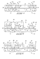
- a semiconductor wafer in process is indicated generally with reference numeral 10.
- Such comprises a bulk monocrystalline silicon substrate 12.
- semiconductor substrate is defined to mean any construction comprising semiconductive material, including, but not limited to, bulk semiconductive materials such as a semiconductive wafer (either alone or in assemblies comprising other materials thereon), and semiconductive material layers (either alone or in assemblies comprising other materials).
- substrate refers to any supporting structure, including, but not limited to, the semiconductor substrates described above.
- a conductively doped semiconductive layer 16 is formed over gate dielectric layer 14.
- Conductively doped polysilicon is one example.
- An insulative capping layer 18 is formed over semiconductive layer 16.
- An example material is again silicon dioxide.
- Intervening conductive layers, such as refractory metal silicides, might of course also be interposed between layers 16 and 18.
- An etch stop layer 20 is formed over insulative capping layer 18.
- An example preferred material is polysilicon.
- LDD implant doping is preferably conducted to provide illustrated implant regions 33 for the transistors.
- One example implant dose for regions 33 would be 2 X 10 13 ions/cm 2 .
- the LDD implant doping can implanted after source/drain regions have been formed (or a combination of both). Forming LDD regions later in the process reduces the D t seen by such implants.
- an insulating layer 34 is deposited over substrate 12 and lines 22, 24 and 26.
- the thickness of layer 34 is preferably chosen to be greater than that of the combined etch stop layer, capping layer and semiconductor layer, and to be received between the transistor gate lines to fill the illustrated cross-sectional area extending between adjacent gate lines.
- Example and preferred materials include undoped silicon dioxide deposited by decomposition of tetraethylorthosilicate, and borophosphosilicate glass.
- insulative material layer 34 has been planarized. Such is preferably accomplished by chemical-mechanical polishing using etch stop layer 20 of gates 22, 24 and 26 as an etch stop for such polishing.
- a layer of photoresist 36 has been deposited and patterned. Insulative material 34 is etched to effectively form contact openings 38, 39 and 40 therein to proximate substrate 12, and preferably effective to outwardly expose material of semiconductor substrate 12.
- the exposed portions of semiconductor substrate 12 are designated as locations 42, 43 and 44.
- the depicted etching constitutes but one example of etching insulating layer 34 proximate lines 22 and 24 along at least a portion of facing sidewalls 28 and 29. Such portion preferably comprises a majority of the depicted sidewalls, and as shown constitutes the entirety of said sidewalls to semiconductor substrate 12.
- the illustrated insulating layer 34 etching is conducted along at least a portion of each of opposing line sidewalls 31 and 32. Further with respect to lines 22 and 24, such etching of insulating layer 34 is conducted along portions of sidewalls 28 and 29, and not along the respective opposing sidewalls 27 and 30. Further, such insulating layer 34 etching exposes conductive material of at least one of the transistor gates, with such etching in the illustrated example exposing conductive material 16 of sidewalls 28, 29, 31 and 32 of the illustrated transistor gates. Further with respect to gate lines 22 and 24, the insulative material is etched to remain/be received over the one sidewalls 27 and 30, and not sidewalls 28 and 29.
- insulating material preferably comprises deposition of an insulating layer 46 over substrate 12; lines 22, 24 and 26; and planarized and etched insulative material 34 to a thickness which less than completely fills at least some of the contact openings.
- insulating layer preferably comprises a spacer forming layer, with silicon dioxide and silicon nitride being but two examples.
- spacer forming layer 46 is anisotropically etched to form insulative sidewall spacers 47, 48, 49, 50 and 52. Such constitutes but one example of forming the illustrated insulative sidewall spacers.
- insulating layer 34 is received between at least one of the sidewalls and one of the sidewall spacers, for example as shown with respect to line 24 between sidewall 30 and spacer 49. Further with respect to this example line 24, insulative material 34 is received between the one sidewall 30 and the one insulative spacer 49 formed thereover, and is not received between the opposing sidewall 29 and the other spacer 48 formed thereover.
- insulative sidewall spacers 48 and 49, and 50 and 52 are formed over each of the respective opposing line sidewalls of lines 24 and 26, wherein in the depicted section only one insulative spacer 47 is formed over one sidewall of line 22.
- insulative material 34 received between sidewall 30 and insulative spacer 49 of line 24 has a maximum lateral thickness which is greater than or equal (greater as shown) to a maximum lateral thickness of sidewall spacer 49. Source/drain implanting may occur at this point in the process, if desired.
- a local interconnect layer 56 is deposited to overlie at least one of the transistor gates, and ultimately interconnect locations 42, 43 and 44 of substrate 12, and is thus provided in electrical connection therewith.
- An example preferred material for layer 56 is polysilicon. Due to the spacing constraints between the insulative spacers of lines 22 and 24 versus that of lines 24 and 26, layer 56 completely fills contact opening area 38 and less than completely fills contact opening areas 39 and 40.
- layer 56 might be in situ conductively doped as deposited and/or separately implanted with conductivity enhancing impurity subsequent to deposition. Further, any such subsequent implantings might be masked to only be provided within portions of layer 56 where, for example, both n-type and p-type substrate regions are being conductively connected by an ultimately conductive interconnect formed from layer 56. Most preferably, interconnect layer 56 will ultimately comprise suitably conductively doped semiconductive material.
- another conductive strapping layer such as a refractory metal silicide, will ideally be formed atop layer 56 to avoid or overcome an inherent parasitic diode that forms where p-type and n-type materials join.
- a conductive dopant diffusion barrier layer might also be provided prior to deposition of layer 56.
- Example preferred implantings whether p-type, n-type, or a combination of the same, is next described still with reference to Fig. 8.
- Such depicts two preferred implantings represented by peak implant locations or depths 58 and 60.
- Such are preferably accomplished by two discrete implantings which provide peak implant location 60 deeper relative to layer 56 than implant 58.
- regions of layer 56 are shown where peak implant 60 is deeper within layer 56 than is peak implant 58.
- the peak implant location or depth for implant 60 is preferably not chosen to be so deep to be within conductively doped material 16 of lines 22, 24 and 26.
- the implanting to produce depicted implant 60 is conducted through local interconnect layer 56 and into semiconductor substrate material 12 therebeneath. Diffusing of the conductivity enhancing impurity provided within layer 56 might ultimately occur from local interconnect layer 56 into semiconductor substrate material 12 therebeneath within locations 42, 43 and 44 to provide the majority of the conductivity enhancing impurity doping for the source/drain regions of the illustrated transistor lines. Depending on the processor's desire and the degree of diffusion, such source/drain regions might principally reside within semiconductor substrate material 12, or reside as elevated source/drain regions within layer 56.
- layer 56 in certain locations acts as a spacer for the deeper implant. Further, such may actually reduce junction capacitance by counter doping halo implants that are further away from gate polysilicon. This can provide flexibility in the settings of the halo implants.
- local interconnect layer 56 is formed (i.e., by photopatterning and etching) into a local interconnect line 57 which overlies at least portions of illustrated conductive lines 24, 26 and 28, and electrically interconnects substrate material locations 42, 43 and 44.
- Fig. 10 illustrates a semiconductor wafer fragment 10a comprising a bulk monocrystalline silicon substrate 12.
- Semiconductor substrate 12 has been patterned to form field isolation region 64 and active area region 62.
- material 66 of field isolation region 64 comprises silicon dioxide fabricated by LOCOS processing. Such might constitute other material and other isolation techniques, for example trench and refill resulting from etching trenches into substrate 12 and depositing oxide such as by CVD, including PECVD.
- Fragment 10a in a preferred and exemplary embodiment comprises an extension of fragment 10 of the first described embodiment, such as an extension in Fig. 10 starting from the far right portion of Fig. 4 of the first described embodiment. Accordingly, insulating layer 34 is shown as having been deposited and planarized,
- a trench 68 is etched into field isolation-material 66 and is received within insulating layer 34. Such includes opposing insulative sidewalls 77 and a base 79. Trench 68 in this illustrated example extends to an edge 70 of isolation material 66 proximate, and here extending to, active area substrate material 12 of region 62. An example preferred depth for trench opening 68 is 10% to 20% greater than the combined thickness of the conductive and insulating materials of gate stacks 22, 24 and 26.
- a conductive material 72 is deposited to at least partially fill trench 68, and electrically connects with substrate material 12 of active area region 62. As shown, material 72 is preferably deposited to overfill trench 68.
- the width of trench 68 is preferably chosen to be more narrow than double the thickness of layer of material 72. Such preferred narrow nature of trench 68 facilitates complete filling thereof with conductive material 72 in spite of its depth potentially being greater than the globally deposited thickness of layer 72.
- conductive layer 72 has been etched to produce the illustrated local interconnect line 75 which includes a line segment 76 received within trench 68 over isolation material 66.
- a small degree of overetch preferably occurs as shown to assure complete removal material 72 from over the outer surface of insulating layer 34.
- the shape of trench 68 is chosen and utilized to define the entire outline and shape of the conductive line being formed relative to isolation material 66.
- conductive material of line 75 preferably contacts material 66 of trench sidewalls 77 and base 79.
- Fig. 17 illustrates an exemplary alternate wafer fragment 10b embodiment corresponding to Fig. 16, but using a trench isolation oxide 66b as opposed to LOCOS oxide 66.
- An exemplary preferred trench filled line 68b is shown.
- a method of fabricating integrated circuitry comprises:
- the etching of the insulating layer (34) is conducted along at least a portion of each of the opposing line sidewalls (31 and 32), the anisotropic etching forming an insulating sidewall spacer (50, 52) over each of the opposing line sidewalls (31, 32).
- the etching of the insulating layer (34) is conducted along the portion of the one sidewall (28) and not along the opposing sidewall (27).
- the portion comprises a majority of said one sidewall (31 or 32).
- the portion comprises the substantial entirety of said at least one sidewall (31 or 32).
- the etching of the insulating layer (34) outwardly exposes material (12) of the semiconductor substrate (12).
- the conductive line (26) is formed to comprise a transistor gate.
- the method of the first related aspect comprises:
- a method of fabricating integrated circuitry comprises:
- the contact opening etching exposes semiconductive material (12) of the semiconductor substrate (12).
- the contact opening etching exposes conductive material (16) of at least one of the pair of transistor gates (22, 24).
- the contact opening etching exposes conductive material (16) of each of the pair of transistor gates (22, 24).
- the contact opening etching exposes conductive material (16) of at least one of the sidewalls (27, 28, 29, 30) of at least one of the pair of transistor gates (22, 24).
- the method of the second related aspect comprises planarizing the insulating layer (34) prior to said etching of it.
- the method of the second related aspect comprises:
- a method of fabricating integrated circuitry comprises:
- the contact opening etching exposes conductive material (16) of each of the one sidewalls (28, 29) of each of the pair of transistor gates (22, 24).
- the covering comprises deposition of an insulating layer (46).
- the covering comprises deposition of an insulating layer (46), and subsequent anisotropic etching thereof.
- the method of the third related aspect comprises planarizing the insulating layer (46) prior to the contact opening etching.
- the method of the third related aspect comprises:
- a method of forming a local interconnect comprises:
- the insulating layer is not received between the other sidewall and the other sidewall spacer.
- the etching exposes semiconductive material (12) of the semiconductor substrate (12) within the first and another contact openings (38, 39).
- the method of the fourth aspect comprises planarizing the insulating layer (34) prior to said etching of it.
- the insulating layer (34) as received between the one sidewall (30) and the one sidewall spacer (49) has a maximum lateral thickness which is greater than or equal to a maximum lateral thickness of the one sidewall spacer (49).
- the local interconnect layer (56) comprises polysilicon .
- the method of the fourth related aspect comprises:
- a method of forming a conductive line (24) comprises:
- a method of forming a local interconnect comprises:
- the method of the sixth related aspect comprises conducting the one implanting relative to another portion of the local interconnect layer (56) to have a peak implant location (60) which is through said layer (56) and within the semiconductor substrate material (12) therebeneath.
- a method of forming a local interconnect comprises:
- the method of the seventh related aspect further comprises in another implanting step separate from said implanting, implanting conductivity enhancing impurity to a peak concentration location (58) which is within the local interconnect layer (56).
- a method of fabricating integrated circuitry comprises:
- a method of forming a conductive line (75, 68b) comprises:
- the method of the ninth related aspect comprises forming the field isolation material (66) to comprise LOCOS oxide.
- the method of the ninth related aspect comprises depositing an insulative layer (34) over the active area (62) and field isolation regions (64), and planarizing the insulative lay er (34) prior to the etching.
- the method of the ninth related aspect comprises depositing an insulative layer (34) over the active area (62) and field isolation regions (64), and planarizing the insulative layer (34) prior to the etching; the etching comprising etching the trench (68) to be received within the planarized insulative layer (34).
- the method of the ninth related aspect comprises forming the field isolation material (66) to comprise CVD oxide formed within etched substrate trenches.
- the conductive material (72) is initially deposited to overfill the trench (68), and comprising removing some of the conductive material (72) after the initial deposition to leave the trench (68) only partially filled with the conductive material (72).
- a method of forming a local interconnect (75) comprises:
- the method of the tenth related aspect comprises forming the field isolation material (66) to comprise LOCOS oxide.
- the method of the tenth related aspect comprises forming the field isolation material (66) to comprise CVD oxide formed within etched substrate trenches.
- the local interconnect layer (72) is initially deposited to overfill the trench (68), and comprising removing some of the interconnect layer (72) after the initial deposition to leave the trench (68) only partially filled with the interconnect layer (72).
- integrated circuitry comprises:
- the field isolation material (66) comprises LOCOS oxide.
- the field isolation material (66) comprises CVD oxide formed within etched substrate trenches.
- the conductive line (75, 68b) within the trench (6 8) is defined by the shape of the trench (68) formed within the field isolation material (66).
- the field isolation material (66) comprises LOCOS oxide. More preferably, in this case, the field isolation material (66) comprises CVD oxide formed within etched substrate trenches.
- the trench (68) has opposing insulative sidewalls (77) comprising the field isolation material (66), conductive material (72) of the line (75, 68b) contacting the trench sidewalls (77).
- integrated circuitry comprises:
- the field isolation material (66) comprises LOCOS oxide.
- the field isolation material (66) comprises CVD oxide formed within etched substrate trenches.
- the conductive line (75, 68b) within the trench (68) is defined by the shape of the trench (68) formed within the field isolation material (66).
- the field isolation material (66) comprises LOCOS oxide. More preferably, in this case, the field isolation material (66) comprises CVD oxide formed within etched substrate trenches to form a particular case.
- the trench (68) has opposing insulative sidewalls (77) comprising the field isolation material (66), conductive material (72) of the local interconnect line (75, 68b) contacting the trench sidewalls (77).
- integrated circuitry comprises:
- the opposing sidewalls (77) extend to a trench base (79) extending between the sidewalls (77).
- the opposing sidewalls (77) extend to a trench base (79) extending between the sidewalls (77), the trench base (79) including a portion which is substantially perpendicular to the sidewall opposing portions.
- the sidewall opposing portions extend to a trench base (79) extending between the sidewalls (77).
- the sidewall opposing portions extend to a trench base (79) extending between the sidewalls (77), the trench base (79) including a portion which is substantially perpendicular to the sidewall opposing portions.
- integrated circuitry comprises:
- the trench base (79) includes a portion which is substantially perpendicular to the sidewalls (77).
- the trench (68) comprises opposing sidewalls (77) having some opposing portions thereof which are substantially parallel with one another.
- the opposing sidewalls (77) extend to a trench base (79) extending between the sidewalls (77). More preferably, in this case, the opposing sidewalls (77) extend to a trench base (79) extending between the sidewalls (77), the trench base (79) including a portion which is substantially perpendicular to the sidewall opposing portions.
- the sidewall opposing portions extend to a trench base (79) extending between the sidewalls (77). Still more preferably, in this case, the sidewall opposing portions extend to a trench base (79) extending between the sidewalls (77), the trench base (79) including a portion which is substantially perpendicular to the sidewall opposing portions.
- the trench (68) comprises opposing sidewalls (77) which extend from an outer surface of the field isolation material (66) substantially parallel with one another to a trench base (79).
- the trench base (79) includes a portion which is substantially perpendicular to the sidewalls (77).
Landscapes
- Internal Circuitry In Semiconductor Integrated Circuit Devices (AREA)
- Insulated Gate Type Field-Effect Transistor (AREA)
- Metal-Oxide And Bipolar Metal-Oxide Semiconductor Integrated Circuits (AREA)
- Element Separation (AREA)
- Local Oxidation Of Silicon (AREA)
Applications Claiming Priority (2)
| Application Number | Priority Date | Filing Date | Title |
|---|---|---|---|
| US09/266,456 US6180494B1 (en) | 1999-03-11 | 1999-03-11 | Integrated circuitry, methods of fabricating integrated circuitry, methods of forming local interconnects, and methods of forming conductive lines |
| EP00913870A EP1177578A1 (de) | 1999-03-11 | 2000-03-10 | Verfahren zur herstellung von lokalverbindungen und leiterbahnen, und resultierende struktur |
Related Parent Applications (1)
| Application Number | Title | Priority Date | Filing Date |
|---|---|---|---|
| EP00913870A Division EP1177578A1 (de) | 1999-03-11 | 2000-03-10 | Verfahren zur herstellung von lokalverbindungen und leiterbahnen, und resultierende struktur |
Publications (3)
| Publication Number | Publication Date |
|---|---|
| EP1775763A2 true EP1775763A2 (de) | 2007-04-18 |
| EP1775763A3 EP1775763A3 (de) | 2008-07-23 |
| EP1775763B1 EP1775763B1 (de) | 2014-06-04 |
Family
ID=23014661
Family Applications (3)
| Application Number | Title | Priority Date | Filing Date |
|---|---|---|---|
| EP06019579.9A Expired - Lifetime EP1775763B1 (de) | 1999-03-11 | 2000-03-10 | Verfahren zur Herstellung von lokalen Interconnects und Leiterbahnen, sowie resultierende Struktur |
| EP06019580A Withdrawn EP1746644A3 (de) | 1999-03-11 | 2000-03-10 | Verfahren zur Herstellung von lokalen Interconnects und Leiterbahnen, sowie resultierende Struktur |
| EP00913870A Withdrawn EP1177578A1 (de) | 1999-03-11 | 2000-03-10 | Verfahren zur herstellung von lokalverbindungen und leiterbahnen, und resultierende struktur |
Family Applications After (2)
| Application Number | Title | Priority Date | Filing Date |
|---|---|---|---|
| EP06019580A Withdrawn EP1746644A3 (de) | 1999-03-11 | 2000-03-10 | Verfahren zur Herstellung von lokalen Interconnects und Leiterbahnen, sowie resultierende Struktur |
| EP00913870A Withdrawn EP1177578A1 (de) | 1999-03-11 | 2000-03-10 | Verfahren zur herstellung von lokalverbindungen und leiterbahnen, und resultierende struktur |
Country Status (6)
| Country | Link |
|---|---|
| US (9) | US6180494B1 (de) |
| EP (3) | EP1775763B1 (de) |
| JP (3) | JP2003533866A (de) |
| KR (1) | KR100435933B1 (de) |
| AU (1) | AU3523200A (de) |
| WO (1) | WO2000054331A1 (de) |
Families Citing this family (28)
| Publication number | Priority date | Publication date | Assignee | Title |
|---|---|---|---|---|
| US6963510B1 (en) * | 1998-07-10 | 2005-11-08 | Xilinx, Inc. | Programmable capacitor and method of operating same |
| US6180494B1 (en) * | 1999-03-11 | 2001-01-30 | Micron Technology, Inc. | Integrated circuitry, methods of fabricating integrated circuitry, methods of forming local interconnects, and methods of forming conductive lines |
| JP3410063B2 (ja) * | 2000-05-15 | 2003-05-26 | 沖電気工業株式会社 | 半導体装置及びその製造方法 |
| US6599789B1 (en) * | 2000-11-15 | 2003-07-29 | Micron Technology, Inc. | Method of forming a field effect transistor |
| US6599824B1 (en) * | 2001-02-26 | 2003-07-29 | Advanced Micro Devices, Inc. | System for and method of forming local interconnect using microcontact printing |
| US7081398B2 (en) * | 2001-10-12 | 2006-07-25 | Micron Technology, Inc. | Methods of forming a conductive line |
| US6727168B2 (en) | 2001-10-24 | 2004-04-27 | Micron Technology, Inc. | Method of forming local interconnects |
| US6716687B2 (en) * | 2002-02-11 | 2004-04-06 | Micron Technology, Inc. | FET having epitaxial silicon growth |
| WO2004041712A2 (en) * | 2002-05-13 | 2004-05-21 | William Marsh Rice University | Method of making a nanoscale electronic device |
| US7071043B2 (en) | 2002-08-15 | 2006-07-04 | Micron Technology, Inc. | Methods of forming a field effect transistor having source/drain material over insulative material |
| US7012021B2 (en) * | 2004-01-29 | 2006-03-14 | Taiwan Semiconductor Mfg | Method for end point detection polysilicon chemical mechanical polishing in an anti-fuse memory device |
| US7176656B2 (en) * | 2004-06-22 | 2007-02-13 | Campbell Hausfeld/Scott Fetzer Company | Tool with battery pack |
| US7118966B2 (en) * | 2004-08-23 | 2006-10-10 | Micron Technology, Inc. | Methods of forming conductive lines |
| US7547945B2 (en) * | 2004-09-01 | 2009-06-16 | Micron Technology, Inc. | Transistor devices, transistor structures and semiconductor constructions |
| JP4848638B2 (ja) * | 2005-01-13 | 2011-12-28 | ソニー株式会社 | 半導体素子の形成方法および半導体素子のマウント方法 |
| US7384849B2 (en) * | 2005-03-25 | 2008-06-10 | Micron Technology, Inc. | Methods of forming recessed access devices associated with semiconductor constructions |
| US7282401B2 (en) | 2005-07-08 | 2007-10-16 | Micron Technology, Inc. | Method and apparatus for a self-aligned recessed access device (RAD) transistor gate |
| US7462534B2 (en) * | 2005-08-02 | 2008-12-09 | Micron Technology, Inc. | Methods of forming memory circuitry |
| US7867851B2 (en) | 2005-08-30 | 2011-01-11 | Micron Technology, Inc. | Methods of forming field effect transistors on substrates |
| US7859112B2 (en) * | 2006-01-13 | 2010-12-28 | Micron Technology, Inc. | Additional metal routing in semiconductor devices |
| US7700441B2 (en) | 2006-02-02 | 2010-04-20 | Micron Technology, Inc. | Methods of forming field effect transistors, methods of forming field effect transistor gates, methods of forming integrated circuitry comprising a transistor gate array and circuitry peripheral to the gate array, and methods of forming integrated circuitry comprising a transistor gate array including first gates and second grounded isolation gates |
| US7859026B2 (en) * | 2006-03-16 | 2010-12-28 | Spansion Llc | Vertical semiconductor device |
| US7602001B2 (en) | 2006-07-17 | 2009-10-13 | Micron Technology, Inc. | Capacitorless one transistor DRAM cell, integrated circuitry comprising an array of capacitorless one transistor DRAM cells, and method of forming lines of capacitorless one transistor DRAM cells |
| US7772632B2 (en) * | 2006-08-21 | 2010-08-10 | Micron Technology, Inc. | Memory arrays and methods of fabricating memory arrays |
| US7589995B2 (en) * | 2006-09-07 | 2009-09-15 | Micron Technology, Inc. | One-transistor memory cell with bias gate |
| US7923373B2 (en) | 2007-06-04 | 2011-04-12 | Micron Technology, Inc. | Pitch multiplication using self-assembling materials |
| US9087839B2 (en) | 2013-03-29 | 2015-07-21 | International Business Machines Corporation | Semiconductor structures with metal lines |
| US10191733B2 (en) * | 2013-06-25 | 2019-01-29 | Sap Se | Software change process orchestration in a runtime environment |
Citations (1)
| Publication number | Priority date | Publication date | Assignee | Title |
|---|---|---|---|---|
| EP0847081A1 (de) | 1996-12-09 | 1998-06-10 | Texas Instruments Incorporated | Verbesserungen in, an oder in Bezug auf Halbleitervorrichtungen |
Family Cites Families (54)
| Publication number | Priority date | Publication date | Assignee | Title |
|---|---|---|---|---|
| JPS55153342A (en) * | 1979-05-18 | 1980-11-29 | Fujitsu Ltd | Semiconductor device and its manufacture |
| US4333227A (en) * | 1979-11-29 | 1982-06-08 | International Business Machines Corporation | Process for fabricating a self-aligned micrometer bipolar transistor device |
| DE3234637A1 (de) * | 1982-09-18 | 1984-03-22 | Alfred Teves Gmbh, 6000 Frankfurt | Verfahren und schaltungsanordnung zur steuerung einer bremsschlupfregelanlage |
| JPS59133944A (ja) | 1983-01-21 | 1984-08-01 | Showa Denko Kk | 合金薄帯の製造方法および製造装置 |
| JPS6054453A (ja) | 1983-09-05 | 1985-03-28 | Oki Electric Ind Co Ltd | 半導体集積回路装置の製造方法 |
| DK583687A (da) * | 1986-11-20 | 1988-05-21 | Draco Ab | Middel til regulering af appetit eller sovemiddel |
| JPH01147829A (ja) * | 1987-12-04 | 1989-06-09 | Toshiba Corp | 半導体装置の製造方法 |
| JPH02148734A (ja) * | 1988-11-29 | 1990-06-07 | Sony Corp | 配線方法及びそれを用いた半導体装置 |
| US5126279A (en) | 1988-12-19 | 1992-06-30 | Micron Technology, Inc. | Single polysilicon cross-coupled resistor, six-transistor SRAM cell design technique |
| KR920005453B1 (ko) | 1989-05-13 | 1992-07-04 | 현대전자산업 주식회사 | 반도체 접속장치 형성방법 |
| JPH0316937A (ja) | 1989-06-13 | 1991-01-24 | Furukawa Electric Co Ltd:The | 光ファイバの製造方法 |
| US5135882A (en) | 1989-07-31 | 1992-08-04 | Micron Technology, Inc. | Technique for forming high-value inter-nodal coupling resistance for rad-hard applications in a double-poly, salicide process using local interconnect |
| JPH03161937A (ja) | 1989-11-21 | 1991-07-11 | Sumitomo Electric Ind Ltd | 電界効果形トランジスタの製造方法 |
| JPH03276727A (ja) * | 1990-03-27 | 1991-12-06 | Nec Corp | 半導体集積回路装置 |
| JPH0492426A (ja) * | 1990-08-08 | 1992-03-25 | Seiko Epson Corp | 半導体装置 |
| US5346836A (en) * | 1991-06-06 | 1994-09-13 | Micron Technology, Inc. | Process for forming low resistance contacts between silicide areas and upper level polysilicon interconnects |
| JP3172229B2 (ja) | 1992-01-23 | 2001-06-04 | 株式会社東芝 | 半導体装置の製造方法 |
| US5356834A (en) * | 1992-03-24 | 1994-10-18 | Kabushiki Kaisha Toshiba | Method of forming contact windows in semiconductor devices |
| KR950011556B1 (ko) * | 1992-07-03 | 1995-10-06 | 현대전자산업주식회사 | 반도체 접속장치 형성방법 |
| KR960002064B1 (ko) | 1992-11-16 | 1996-02-10 | 현대전자산업주식회사 | 반도체 소자의 콘택 제조방법 |
| JP2787646B2 (ja) * | 1992-11-27 | 1998-08-20 | 三菱電機株式会社 | 半導体装置の製造方法 |
| US5346585A (en) * | 1993-04-20 | 1994-09-13 | Micron Semiconductor, Inc. | Use of a faceted etch process to eliminate stringers |
| US5356845A (en) * | 1993-05-11 | 1994-10-18 | Exxon Research And Engineering Company | Process for the reactivation of nickel-alumina catalysts |
| JPH06333944A (ja) * | 1993-05-25 | 1994-12-02 | Nippondenso Co Ltd | 半導体装置 |
| US5776827A (en) * | 1993-08-27 | 1998-07-07 | Yamaha Corporation | Wiring-forming method |
| US5494841A (en) | 1993-10-15 | 1996-02-27 | Micron Semiconductor, Inc. | Split-polysilicon CMOS process for multi-megabit dynamic memories incorporating stacked container capacitor cells |
| JP2809080B2 (ja) | 1993-12-15 | 1998-10-08 | 日本電気株式会社 | 半導体装置の製造方法 |
| KR0137974B1 (ko) * | 1994-01-19 | 1998-06-15 | 김주용 | 반도체 장치 및 그 제조방법 |
| DE4419431C1 (de) * | 1994-06-03 | 1995-04-27 | Goldschmidt Ag Th | Polyolefine, Polyolefin-Blends und elastomermodifizierte Polyolefine mit erhöhter Oberflächenpolarität, Verfahren zu ihrer Herstellung, sowie deren Verwendung |
| US5665520A (en) | 1994-06-13 | 1997-09-09 | Matsushita Electric Industrial Co., Ltd. | Optical recording medium |
| JP2600621B2 (ja) * | 1994-09-14 | 1997-04-16 | 日本電気株式会社 | 半導体装置の製造方法 |
| JP2663900B2 (ja) * | 1995-02-28 | 1997-10-15 | 日本電気株式会社 | 半導体装置の製造方法 |
| JP3161937B2 (ja) | 1995-05-26 | 2001-04-25 | シャープ株式会社 | 携帯型通信装置 |
| US5589415A (en) * | 1995-06-07 | 1996-12-31 | Sgs-Thomson Microelectronics, Inc. | Method for forming a semiconductor structure with self-aligned contacts |
| US6917083B1 (en) | 1995-07-27 | 2005-07-12 | Micron Technology, Inc. | Local ground and VCC connection in an SRAM cell |
| US5734179A (en) | 1995-12-12 | 1998-03-31 | Advanced Micro Devices, Inc. | SRAM cell having single layer polysilicon thin film transistors |
| US5717242A (en) | 1996-04-17 | 1998-02-10 | Advanced Micro Devices, Inc. | Integrated circuit having local interconnect for reduing signal cross coupled noise |
| US5793088A (en) * | 1996-06-18 | 1998-08-11 | Integrated Device Technology, Inc. | Structure for controlling threshold voltage of MOSFET |
| US6033969A (en) * | 1996-09-30 | 2000-03-07 | Taiwan Semiconductor Manufacturing Co., Ltd. | Method of forming a shallow trench isolation that has rounded and protected corners |
| US6077763A (en) * | 1996-11-19 | 2000-06-20 | United Microelectronics Corp. | Process for fabricating a self-aligned contact |
| US5849622A (en) * | 1997-03-07 | 1998-12-15 | Advanced Micro Devices, Inc. | Method of forming a source implant at a contact masking step of a process flow |
| US5789316A (en) * | 1997-03-10 | 1998-08-04 | Vanguard International Semiconductor Corporation | Self-aligned method for forming a narrow via |
| US5899732A (en) | 1997-04-11 | 1999-05-04 | Advanced Micro Devices, Inc. | Method of implanting silicon through a polysilicon gate for punchthrough control of a semiconductor device |
| JPH1154724A (ja) | 1997-08-06 | 1999-02-26 | Sony Corp | 半導体装置の製造方法 |
| US5883010A (en) * | 1997-08-07 | 1999-03-16 | National Semiconductor Corporation | Method for protecting nonsilicided surfaces from silicide formation using spacer oxide mask |
| US5801082A (en) | 1997-08-18 | 1998-09-01 | Vanguard International Semiconductor Corporation | Method for making improved shallow trench isolation with dielectric studs for semiconductor integrated circuits |
| JPH11186389A (ja) * | 1997-12-24 | 1999-07-09 | Mitsubishi Electric Corp | 半導体装置およびその製造方法 |
| JPH11251318A (ja) * | 1998-03-06 | 1999-09-17 | Fujitsu Ltd | 半導体装置及びその製造方法 |
| US5899721A (en) | 1998-03-09 | 1999-05-04 | Advanced Micro Devices, Inc. | Method of based spacer formation for ultra-small sapcer geometries |
| US6225875B1 (en) | 1998-10-06 | 2001-05-01 | Hughes Electronics Corporation | Dual sidewall coupled orthomode transducer having septum offset from the transducer axis |
| US6255215B1 (en) * | 1998-10-20 | 2001-07-03 | Advanced Micro Services | Semiconductor device having silicide layers formed using a collimated metal layer |
| TW411566B (en) * | 1998-11-18 | 2000-11-11 | Taiwan Semiconductor Mfg | Process of forming the SAC Plug for self-aligned contact hole |
| US6180494B1 (en) | 1999-03-11 | 2001-01-30 | Micron Technology, Inc. | Integrated circuitry, methods of fabricating integrated circuitry, methods of forming local interconnects, and methods of forming conductive lines |
| US6177318B1 (en) * | 1999-10-18 | 2001-01-23 | Halo Lsi Design & Device Technology, Inc. | Integration method for sidewall split gate monos transistor |
-
1999
- 1999-03-11 US US09/266,456 patent/US6180494B1/en not_active Expired - Lifetime
- 1999-05-21 US US09/316,330 patent/US6225675B1/en not_active Expired - Lifetime
-
2000
- 2000-03-10 JP JP2000604460A patent/JP2003533866A/ja active Pending
- 2000-03-10 WO PCT/US2000/006248 patent/WO2000054331A1/en not_active Ceased
- 2000-03-10 EP EP06019579.9A patent/EP1775763B1/de not_active Expired - Lifetime
- 2000-03-10 EP EP06019580A patent/EP1746644A3/de not_active Withdrawn
- 2000-03-10 EP EP00913870A patent/EP1177578A1/de not_active Withdrawn
- 2000-03-10 AU AU35232/00A patent/AU3523200A/en not_active Abandoned
- 2000-03-10 KR KR10-2001-7011450A patent/KR100435933B1/ko not_active Expired - Fee Related
- 2000-06-29 US US09/608,333 patent/US6391726B1/en not_active Expired - Lifetime
-
2001
- 2001-08-31 US US09/944,894 patent/US6610587B2/en not_active Expired - Lifetime
-
2002
- 2002-02-28 US US10/087,147 patent/US6638842B2/en not_active Expired - Lifetime
-
2003
- 2003-04-17 US US10/418,540 patent/US6803286B2/en not_active Expired - Fee Related
- 2003-07-29 US US10/630,433 patent/US6797600B2/en not_active Expired - Fee Related
- 2003-12-05 US US10/729,260 patent/US6982203B2/en not_active Expired - Fee Related
-
2004
- 2004-11-10 US US10/986,415 patent/US7094636B2/en not_active Expired - Fee Related
-
2006
- 2006-02-28 JP JP2006054044A patent/JP2006203232A/ja not_active Withdrawn
- 2006-02-28 JP JP2006053994A patent/JP2006203231A/ja not_active Withdrawn
Patent Citations (1)
| Publication number | Priority date | Publication date | Assignee | Title |
|---|---|---|---|---|
| EP0847081A1 (de) | 1996-12-09 | 1998-06-10 | Texas Instruments Incorporated | Verbesserungen in, an oder in Bezug auf Halbleitervorrichtungen |
Also Published As
| Publication number | Publication date |
|---|---|
| US7094636B2 (en) | 2006-08-22 |
| AU3523200A (en) | 2000-09-28 |
| WO2000054331A9 (en) | 2003-06-19 |
| US20040115914A1 (en) | 2004-06-17 |
| US6391726B1 (en) | 2002-05-21 |
| US6225675B1 (en) | 2001-05-01 |
| US6803286B2 (en) | 2004-10-12 |
| US20020102844A1 (en) | 2002-08-01 |
| EP1177578A1 (de) | 2002-02-06 |
| US6610587B2 (en) | 2003-08-26 |
| US20040018710A1 (en) | 2004-01-29 |
| EP1746644A3 (de) | 2007-10-10 |
| US20030203548A1 (en) | 2003-10-30 |
| KR100435933B1 (ko) | 2004-06-12 |
| US6638842B2 (en) | 2003-10-28 |
| KR20020007323A (ko) | 2002-01-26 |
| WO2000054331A1 (en) | 2000-09-14 |
| US6180494B1 (en) | 2001-01-30 |
| EP1775763A3 (de) | 2008-07-23 |
| JP2003533866A (ja) | 2003-11-11 |
| US20050098531A1 (en) | 2005-05-12 |
| US6982203B2 (en) | 2006-01-03 |
| US20020048865A1 (en) | 2002-04-25 |
| EP1775763B1 (de) | 2014-06-04 |
| JP2006203232A (ja) | 2006-08-03 |
| JP2006203231A (ja) | 2006-08-03 |
| EP1746644A2 (de) | 2007-01-24 |
| US6797600B2 (en) | 2004-09-28 |
Similar Documents
| Publication | Publication Date | Title |
|---|---|---|
| US6180494B1 (en) | Integrated circuitry, methods of fabricating integrated circuitry, methods of forming local interconnects, and methods of forming conductive lines | |
| JP2705716B2 (ja) | Dramセルの製造方法 | |
| US7675110B2 (en) | Semiconductor device and method of manufacturing the same | |
| JP3691963B2 (ja) | 半導体装置及びその製造方法 | |
| US6432774B2 (en) | Method of fabricating memory cell with trench capacitor and vertical transistor | |
| US6548394B1 (en) | Method of forming contact plugs | |
| US6534359B2 (en) | Method of fabricating memory cell | |
| US20010012673A1 (en) | Mos transistor having self-aligned well bias area and method of fabricating the same | |
| US6261924B1 (en) | Maskless process for self-aligned contacts | |
| US5998269A (en) | Technology for high performance buried contact and tungsten polycide gate integration | |
| KR100318320B1 (ko) | 반도체장치의 제조방법 | |
| US6376887B2 (en) | Semiconductor memory having buried digit lines | |
| KR100620196B1 (ko) | 반도체 소자의 제조 방법 | |
| KR950012916B1 (ko) | 반도체장치의 소자분리방법 | |
| KR20040019172A (ko) | 반도체 장치의 콘택 플러그 및 그 형성 방법 | |
| JP2004047525A (ja) | コンタクトホール形成方法 | |
| KR20070016740A (ko) | 반도체 소자 및 이의 제조방법 |
Legal Events
| Date | Code | Title | Description |
|---|---|---|---|
| PUAI | Public reference made under article 153(3) epc to a published international application that has entered the european phase |
Free format text: ORIGINAL CODE: 0009012 |
|
| 17P | Request for examination filed |
Effective date: 20060927 |
|
| AC | Divisional application: reference to earlier application |
Ref document number: 1177578 Country of ref document: EP Kind code of ref document: P |
|
| AK | Designated contracting states |
Kind code of ref document: A2 Designated state(s): AT BE CH CY DE DK ES FI FR GB GR IE IT LI LU MC NL PT SE |
|
| AX | Request for extension of the european patent |
Extension state: AL LT LV MK RO SI |
|
| PUAL | Search report despatched |
Free format text: ORIGINAL CODE: 0009013 |
|
| AK | Designated contracting states |
Kind code of ref document: A3 Designated state(s): AT BE CH CY DE DK ES FI FR GB GR IE IT LI LU MC NL PT SE |
|
| AX | Request for extension of the european patent |
Extension state: AL LT LV MK RO SI |
|
| AKX | Designation fees paid |
Designated state(s): AT BE CH CY DE DK ES FI FR GB GR IE IT LI LU MC NL PT SE |
|
| 17Q | First examination report despatched |
Effective date: 20090415 |
|
| RAP1 | Party data changed (applicant data changed or rights of an application transferred) |
Owner name: ROUND ROCK RESEARCH, LLC |
|
| GRAP | Despatch of communication of intention to grant a patent |
Free format text: ORIGINAL CODE: EPIDOSNIGR1 |
|
| INTG | Intention to grant announced |
Effective date: 20130715 |
|
| GRAP | Despatch of communication of intention to grant a patent |
Free format text: ORIGINAL CODE: EPIDOSNIGR1 |
|
| INTG | Intention to grant announced |
Effective date: 20140207 |
|
| GRAS | Grant fee paid |
Free format text: ORIGINAL CODE: EPIDOSNIGR3 |
|
| GRAA | (expected) grant |
Free format text: ORIGINAL CODE: 0009210 |
|
| AC | Divisional application: reference to earlier application |
Ref document number: 1177578 Country of ref document: EP Kind code of ref document: P |
|
| AK | Designated contracting states |
Kind code of ref document: B1 Designated state(s): AT BE CH CY DE DK ES FI FR GB GR IE IT LI LU MC NL PT SE |
|
| REG | Reference to a national code |
Ref country code: GB Ref legal event code: FG4D |
|
| REG | Reference to a national code |
Ref country code: CH Ref legal event code: EP |
|
| REG | Reference to a national code |
Ref country code: AT Ref legal event code: REF Ref document number: 671509 Country of ref document: AT Kind code of ref document: T Effective date: 20140615 |
|
| REG | Reference to a national code |
Ref country code: IE Ref legal event code: FG4D |
|
| REG | Reference to a national code |
Ref country code: DE Ref legal event code: R096 Ref document number: 60048604 Country of ref document: DE Effective date: 20140717 |
|
| REG | Reference to a national code |
Ref country code: AT Ref legal event code: MK05 Ref document number: 671509 Country of ref document: AT Kind code of ref document: T Effective date: 20140604 |
|
| REG | Reference to a national code |
Ref country code: NL Ref legal event code: VDEP Effective date: 20140604 |
|
| PG25 | Lapsed in a contracting state [announced via postgrant information from national office to epo] |
Ref country code: FI Free format text: LAPSE BECAUSE OF FAILURE TO SUBMIT A TRANSLATION OF THE DESCRIPTION OR TO PAY THE FEE WITHIN THE PRESCRIBED TIME-LIMIT Effective date: 20140604 Ref country code: GR Free format text: LAPSE BECAUSE OF FAILURE TO SUBMIT A TRANSLATION OF THE DESCRIPTION OR TO PAY THE FEE WITHIN THE PRESCRIBED TIME-LIMIT Effective date: 20140905 Ref country code: CY Free format text: LAPSE BECAUSE OF FAILURE TO SUBMIT A TRANSLATION OF THE DESCRIPTION OR TO PAY THE FEE WITHIN THE PRESCRIBED TIME-LIMIT Effective date: 20140604 |
|
| PG25 | Lapsed in a contracting state [announced via postgrant information from national office to epo] |
Ref country code: SE Free format text: LAPSE BECAUSE OF FAILURE TO SUBMIT A TRANSLATION OF THE DESCRIPTION OR TO PAY THE FEE WITHIN THE PRESCRIBED TIME-LIMIT Effective date: 20140604 Ref country code: AT Free format text: LAPSE BECAUSE OF FAILURE TO SUBMIT A TRANSLATION OF THE DESCRIPTION OR TO PAY THE FEE WITHIN THE PRESCRIBED TIME-LIMIT Effective date: 20140604 |
|
| PG25 | Lapsed in a contracting state [announced via postgrant information from national office to epo] |
Ref country code: ES Free format text: LAPSE BECAUSE OF FAILURE TO SUBMIT A TRANSLATION OF THE DESCRIPTION OR TO PAY THE FEE WITHIN THE PRESCRIBED TIME-LIMIT Effective date: 20140604 Ref country code: PT Free format text: LAPSE BECAUSE OF FAILURE TO SUBMIT A TRANSLATION OF THE DESCRIPTION OR TO PAY THE FEE WITHIN THE PRESCRIBED TIME-LIMIT Effective date: 20141006 |
|
| PG25 | Lapsed in a contracting state [announced via postgrant information from national office to epo] |
Ref country code: NL Free format text: LAPSE BECAUSE OF FAILURE TO SUBMIT A TRANSLATION OF THE DESCRIPTION OR TO PAY THE FEE WITHIN THE PRESCRIBED TIME-LIMIT Effective date: 20140604 |
|
| REG | Reference to a national code |
Ref country code: DE Ref legal event code: R097 Ref document number: 60048604 Country of ref document: DE |
|
| REG | Reference to a national code |
Ref country code: FR Ref legal event code: PLFP Year of fee payment: 16 |
|
| PLBE | No opposition filed within time limit |
Free format text: ORIGINAL CODE: 0009261 |
|
| STAA | Information on the status of an ep patent application or granted ep patent |
Free format text: STATUS: NO OPPOSITION FILED WITHIN TIME LIMIT |
|
| PG25 | Lapsed in a contracting state [announced via postgrant information from national office to epo] |
Ref country code: DK Free format text: LAPSE BECAUSE OF FAILURE TO SUBMIT A TRANSLATION OF THE DESCRIPTION OR TO PAY THE FEE WITHIN THE PRESCRIBED TIME-LIMIT Effective date: 20140604 Ref country code: IT Free format text: LAPSE BECAUSE OF FAILURE TO SUBMIT A TRANSLATION OF THE DESCRIPTION OR TO PAY THE FEE WITHIN THE PRESCRIBED TIME-LIMIT Effective date: 20140604 |
|
| PGFP | Annual fee paid to national office [announced via postgrant information from national office to epo] |
Ref country code: DE Payment date: 20150305 Year of fee payment: 16 |
|
| 26N | No opposition filed |
Effective date: 20150305 |
|
| PGFP | Annual fee paid to national office [announced via postgrant information from national office to epo] |
Ref country code: FR Payment date: 20150309 Year of fee payment: 16 Ref country code: GB Payment date: 20150304 Year of fee payment: 16 |
|
| REG | Reference to a national code |
Ref country code: DE Ref legal event code: R097 Ref document number: 60048604 Country of ref document: DE Effective date: 20150305 |
|
| PG25 | Lapsed in a contracting state [announced via postgrant information from national office to epo] |
Ref country code: BE Free format text: LAPSE BECAUSE OF FAILURE TO SUBMIT A TRANSLATION OF THE DESCRIPTION OR TO PAY THE FEE WITHIN THE PRESCRIBED TIME-LIMIT Effective date: 20140604 |
|
| PG25 | Lapsed in a contracting state [announced via postgrant information from national office to epo] |
Ref country code: MC Free format text: LAPSE BECAUSE OF FAILURE TO SUBMIT A TRANSLATION OF THE DESCRIPTION OR TO PAY THE FEE WITHIN THE PRESCRIBED TIME-LIMIT Effective date: 20140604 Ref country code: LU Free format text: LAPSE BECAUSE OF FAILURE TO SUBMIT A TRANSLATION OF THE DESCRIPTION OR TO PAY THE FEE WITHIN THE PRESCRIBED TIME-LIMIT Effective date: 20150310 |
|
| REG | Reference to a national code |
Ref country code: CH Ref legal event code: PL |
|
| REG | Reference to a national code |
Ref country code: IE Ref legal event code: MM4A |
|
| PG25 | Lapsed in a contracting state [announced via postgrant information from national office to epo] |
Ref country code: IE Free format text: LAPSE BECAUSE OF NON-PAYMENT OF DUE FEES Effective date: 20150310 Ref country code: LI Free format text: LAPSE BECAUSE OF NON-PAYMENT OF DUE FEES Effective date: 20150331 Ref country code: CH Free format text: LAPSE BECAUSE OF NON-PAYMENT OF DUE FEES Effective date: 20150331 |
|
| REG | Reference to a national code |
Ref country code: DE Ref legal event code: R119 Ref document number: 60048604 Country of ref document: DE |
|
| GBPC | Gb: european patent ceased through non-payment of renewal fee |
Effective date: 20160310 |
|
| REG | Reference to a national code |
Ref country code: FR Ref legal event code: ST Effective date: 20161130 |
|
| PG25 | Lapsed in a contracting state [announced via postgrant information from national office to epo] |
Ref country code: GB Free format text: LAPSE BECAUSE OF NON-PAYMENT OF DUE FEES Effective date: 20160310 Ref country code: FR Free format text: LAPSE BECAUSE OF NON-PAYMENT OF DUE FEES Effective date: 20160331 Ref country code: DE Free format text: LAPSE BECAUSE OF NON-PAYMENT OF DUE FEES Effective date: 20161001 |