US7081398B2 - Methods of forming a conductive line - Google Patents
Methods of forming a conductive line Download PDFInfo
- Publication number
- US7081398B2 US7081398B2 US09/976,635 US97663501A US7081398B2 US 7081398 B2 US7081398 B2 US 7081398B2 US 97663501 A US97663501 A US 97663501A US 7081398 B2 US7081398 B2 US 7081398B2
- Authority
- US
- United States
- Prior art keywords
- trench
- isolation
- line
- forming
- depositing
- Prior art date
- Legal status (The legal status is an assumption and is not a legal conclusion. Google has not performed a legal analysis and makes no representation as to the accuracy of the status listed.)
- Expired - Lifetime, expires
Links
Images


Classifications
-
- H—ELECTRICITY
- H01—ELECTRIC ELEMENTS
- H01L—SEMICONDUCTOR DEVICES NOT COVERED BY CLASS H10
- H01L21/00—Processes or apparatus adapted for the manufacture or treatment of semiconductor or solid state devices or of parts thereof
- H01L21/70—Manufacture or treatment of devices consisting of a plurality of solid state components formed in or on a common substrate or of parts thereof; Manufacture of integrated circuit devices or of parts thereof
- H01L21/71—Manufacture of specific parts of devices defined in group H01L21/70
- H01L21/768—Applying interconnections to be used for carrying current between separate components within a device comprising conductors and dielectrics
- H01L21/76838—Applying interconnections to be used for carrying current between separate components within a device comprising conductors and dielectrics characterised by the formation and the after-treatment of the conductors
- H01L21/76895—Local interconnects; Local pads, as exemplified by patent document EP0896365
-
- H—ELECTRICITY
- H01—ELECTRIC ELEMENTS
- H01L—SEMICONDUCTOR DEVICES NOT COVERED BY CLASS H10
- H01L23/00—Details of semiconductor or other solid state devices
- H01L23/52—Arrangements for conducting electric current within the device in operation from one component to another, i.e. interconnections, e.g. wires, lead frames
- H01L23/535—Arrangements for conducting electric current within the device in operation from one component to another, i.e. interconnections, e.g. wires, lead frames including internal interconnections, e.g. cross-under constructions
-
- H—ELECTRICITY
- H01—ELECTRIC ELEMENTS
- H01L—SEMICONDUCTOR DEVICES NOT COVERED BY CLASS H10
- H01L2924/00—Indexing scheme for arrangements or methods for connecting or disconnecting semiconductor or solid-state bodies as covered by H01L24/00
- H01L2924/0001—Technical content checked by a classifier
- H01L2924/0002—Not covered by any one of groups H01L24/00, H01L24/00 and H01L2224/00
Definitions
- This invention relates to methods of forming conductive lines, and to integrated circuitry.
- DRAMs dynamic random access memories
- SRAMs static random access memories
- logic and other circuitry is a continuing goal in semiconductor fabrication.
- Implementing electric circuits involves connecting isolated devices through specific electric paths.
- conductor devices built into semiconductive substrates need to be isolated from one another. Such isolation typically occurs in the form of LOCOS grown field oxide, and more recently in isolation trench and refill field isolation regions.
- Conductive lines for example transistor gate lines, are formed over substrates. Some lines run globally over large areas of the substrate. Others are much shorter and associated with very small portions of the integrated circuitry. This invention was principally motivated in making processing and structural improvements involving local interconnects.
- a method of forming a local interconnect includes forming an isolation trench within a semiconductor substrate.
- a first trench isolation material is deposited over the semiconductor substrate and to within the isolation trench.
- First trench isolation material is removed effective to form a line trench within the isolation material into a desired local interconnect configuration.
- Conductive material is formed within the line trench.
- a second trench isolation material is deposited over the first trench isolation material, over the conductive material within the isolation trench and within the line trench. At least some first and second trench isolation material is removed from the substrate in at least one common removing step.
- a method of forming a local interconnect includes providing a bulk semiconductor substrate having a first conductivity type background region, an adjacent second conductivity type background region and a boundary extending therebetween. An isolation trench is formed within the bulk semiconductor substrate over and along the boundary. A trench isolation material is deposited over the bulk semiconductor substrate and to within the isolation trench. Trench isolation is removed effective to form a line trench within the isolation material into a desired local interconnect configuration. Conductive material is formed to within the line trench.
- integrated circuitry includes a semiconductor substrate comprising trench isolation material.
- a local interconnect line is received within a trench formed within the trench isolation material.
- the local interconnect line includes at least two different conductive materials. One of the conductive materials lines the trench. Another of the conductive materials is received within a conductive trench formed by the one.
- FIG. 1 is a schematic of exemplary integrated circuitry.
- FIG. 2 is a diagrammatic sectional view of a semiconductor wafer fragment in process in accordance with an aspect of the invention.
- FIG. 3 is a view of the FIG. 2 wafer fragment at a processing step subsequent to that shown by FIG. 2 .
- FIG. 4 is a view of the FIG. 3 wafer fragment at a processing step subsequent to that shown by FIG. 3 .
- FIG. 5 is a view of the FIG. 4 wafer fragment at a processing step subsequent to that shown by FIG. 4 .
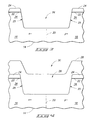
- FIG. 6 is a top plan view of a larger portion of the wafer fragment in process, the above fragmentary views being taken through line X—X in FIG. 6 .
- FIG. 7 is a view of the FIG. 5 wafer fragment at a processing step subsequent to that shown by FIG. 5 .
- FIG. 8 is a view of the FIG. 7 wafer fragment at a processing step subsequent to that shown by FIG. 7 .
- FIG. 9 is a view of the FIG. 8 wafer fragment at a processing step subsequent to that shown by FIG. 8 .
- FIG. 10 is a view of the FIG. 9 wafer fragment at a processing step subsequent to that shown by FIG. 9 .
- FIG. 11 is a top plan view like FIG. 6 , but shown at a processing step subsequent to that of FIGS. 6 and 10 .
- FIG. 12 is a view of a portion of the FIG. 11 wafer fragment as taken through line 12 — 12 in FIG. 11 .
- FIG. 13 is a view of the FIG. 12 wafer fragment at a processing step subsequent to that shown by FIG. 12 .
- the invention contemplates methods of forming local interconnects, and any integrated circuitry involving a local interconnect line, in accordance with the literal wording of the claims.
- the invention is described with respect to but one exemplary integrated circuit shown in FIG. 1 .
- Such depicts a cross-coupled inverter circuitry 10 comprising n-type transistors T 1 n and T 2 n, and p-type transistors T 3 p and T 4 p.
- a local interconnect LI interconnects the gates of T 2 n and T 4 p with source/drain regions of T 1 n and T 3 p.
- a semiconductor wafer fragment is indicated generally with reference 12 .
- Such comprises a bulk semiconductor substrate having a first conductivity-type background region 16 adjacent a second conductivity-type background region 18 , and a boundary 20 extending therebetween.
- An exemplary preferred material for bulk substrate 14 is monocrystalline, for example monocrystalline silicon, with region 16 being shown lightly background doped with “n” type impurity and region 18 being lightly background doped with “p” type impurity.
- semiconductor substrate or “semiconductive substrate” is defined to mean any construction comprising semiconductive material, including, but not limited to, bulk semiconductive materials such as a semiconductive wafer (either alone or in assemblies comprising other materials thereon), and semiconductive material layers (either alone or in assemblies comprising other materials).
- substrate refers to any supporting structure, including, but not limited to, the semiconductive substrates described above.
- layer and “material” encompass both the singular and the plural unless otherwise indicated.
- a pad oxide layer 22 is formed over bulk substrate 14 .
- An exemplary thickness is 100 Angstroms.
- a masking layer 24 is formed over layer 22 .
- An exemplary material is silicon nitride deposited to an exemplary thickness of 900 Angstroms.
- an isolation trench 26 is formed within bulk semiconductor substrate material 14 , which is laterally centered and extends along p-type/n-type boundary 20 . Such will be utilized to form interwell isolation, with an exemplary open width of depicted trench 26 being about 0.5 micron. An exemplary depth within substrate material 14 is 3000 Angstroms. Such provides but one example of forming an isolation trench within a semiconductor substrate. Further in the depicted and preferred embodiment, the isolation trench is formed in bulk substrate material, although the invention is in no way so limited. For purposes of the continuing discussion, isolation trench 26 can be considered as having opposing longitudinal sidewalls 25 in the depicted cross-section. Further in the depicted embodiment, isolation trench 26 is formed to be laterally centered over boundary 20 .
- a first trench isolation material 28 is deposited over substrate 14 and within isolation trench 26 .
- a preferred method of forming layer 28 is by high density plasma chemical vapor deposition.
- Sidewalls 25 of trench 26 are preferably thermally oxidized (not shown) before or after deposition of material 28 .
- exemplary active areas 34 can be seen.
- First trench isolation material 28 is removed effective to form a line trench 30 within the isolation material into a desired local interconnect configuration.
- Such removing preferably comprises photolithography and chemical etching, and forms at least a portion of line trench 30 to be laterally centered within isolation trench 26 between sidewalls 25 , and laterally centered over boundary 20 .
- FIG. 6 depicts that line trench 30 includes extensions 32 which do not extend to an edge of the trench isolation material proximate active area substrate material/regions 34 . Accordingly at this point in the process in the preferred embodiment, local interconnect trench 30 does not extend to connect with the illustrated active areas.
- FIG. 6 also depicts exemplary transistor gate outlines 36 , which would typically not be formed at this point in the preferred embodiment process. Regardless, it can be seen that the far right illustrated edge of local interconnect trench 30 is also spaced from, and therefore does not connect with, the right illustrated transistor gate outline 36 , in this preferred embodiment.
- Conductive material is formed within trench 30 to form at least a portion of the local interconnect being formed.
- FIG. 7 illustrates but one exemplary embodiment wherein a first conductive material 40 is formed, preferably by depositing, to within trench 30 to form a conductive lining therewithin.
- layer 40 is formed of an oxidation resistant material.
- Exemplary materials include tungsten silicide and nitrogen-rich titanium nitride. In such preferred embodiment, such thereby forms an oxidation resistant lining within line trench 30 .
- the oxidation resistant liner material might be insulative as opposed to conductive.
- An exemplary insulative oxidation resistant liner material is silicon nitride.
- a second conductive material 42 is deposited to within line trench 30 on (in contact with) conductive lining 40 .
- Exemplary materials for layer 42 include tungsten and doped polysilicon. Of course, a single conductive material could be utilized or more than two conductive materials utilized.
- conductive materials 40 / 42 are recessed within line trench 30 after their deposition.
- An exemplary preferred process for doing so would be one or more suitable timed chemical etching(s). Such provides but a few preferred examples of forming conductive materials to within line trench 30 .
- a second trench isolation material 46 is deposited over first trench isolation material 28 , over recessed conductive material 40 / 42 within isolation trench 26 , and within line trench 30 .
- Second trench isolation material 46 might be the same composition as first trench isolation material 28 , or be of different composition. More preferably, such are the same material, with high density plasma deposited oxide being the preferred example.
- second trench isolation material 46 is formed on (in contact with) conductive materials 40 / 42 .
- a preferred process includes chemical mechanical polishing (CMP).
- CMP chemical mechanical polishing
- polishing is shown conducted effective to substantially stop on nitride masking layer 24 .
- polishing could also be continued to remove more material, for example polishing through nitride layer 24 and pad oxide layer 22 .
- nitride layer 24 and pad oxide layer 22 might be selectively chemically etched in processing subsequent to that depicted by FIG. 10 .
- an insulative material 50 is formed over trench isolation material 28 / 46 and over conductive material 40 / 42 .
- Exemplary materials for layer 50 include undoped and doped oxides, for example borophosphosilicate glass, phosphosilicate glass, and other doped and undoped silicon dioxides.
- gate lines 36 have been fabricated prior to deposition of layer 50 , and layers 24 and 22 have been removed.
- Contact openings 52 are etched into insulative material 46 and 50 to bridge over and between active area substrate material 34 and conductive material 40 / 42 within line trench 30 .
- a conductor is formed within contact openings 52 which electrically connects the conductive material with the active area substrate material, and with the far right illustrated gate 52 as shown in FIG. 6 . Such thereby effectively extends the conductive local interconnect line to electrically connect with the depicted source/drain regions and transistor gate line.
- the invention also contemplates integrated circuitry comprising a local interconnect line independent of any method of fabrication.
- the invention may have particular application in the formation of local interconnects in the periphery of SRAM circuitry.
- Processing and circuitry in accordance with the invention can serve to provide an extra level of interconnect, thereby freeing up space for higher level interconnects at upper levels of the fabrication. By embedding an extra level of interconnect in trench isolation areas, tighter metallization and interconnect density might be achievable.
Abstract
Description
Claims (39)
Priority Applications (3)
| Application Number | Priority Date | Filing Date | Title |
|---|---|---|---|
| US09/976,635 US7081398B2 (en) | 2001-10-12 | 2001-10-12 | Methods of forming a conductive line |
| US10/222,305 US6867497B2 (en) | 2001-10-12 | 2002-08-15 | Integrated circuitry |
| US11/079,974 US20050156273A1 (en) | 2001-10-12 | 2005-03-14 | Memory devices |
Applications Claiming Priority (1)
| Application Number | Priority Date | Filing Date | Title |
|---|---|---|---|
| US09/976,635 US7081398B2 (en) | 2001-10-12 | 2001-10-12 | Methods of forming a conductive line |
Related Child Applications (1)
| Application Number | Title | Priority Date | Filing Date |
|---|---|---|---|
| US10/222,305 Division US6867497B2 (en) | 2001-10-12 | 2002-08-15 | Integrated circuitry |
Publications (2)
| Publication Number | Publication Date |
|---|---|
| US20030071356A1 US20030071356A1 (en) | 2003-04-17 |
| US7081398B2 true US7081398B2 (en) | 2006-07-25 |
Family
ID=25524314
Family Applications (3)
| Application Number | Title | Priority Date | Filing Date |
|---|---|---|---|
| US09/976,635 Expired - Lifetime US7081398B2 (en) | 2001-10-12 | 2001-10-12 | Methods of forming a conductive line |
| US10/222,305 Expired - Lifetime US6867497B2 (en) | 2001-10-12 | 2002-08-15 | Integrated circuitry |
| US11/079,974 Abandoned US20050156273A1 (en) | 2001-10-12 | 2005-03-14 | Memory devices |
Family Applications After (2)
| Application Number | Title | Priority Date | Filing Date |
|---|---|---|---|
| US10/222,305 Expired - Lifetime US6867497B2 (en) | 2001-10-12 | 2002-08-15 | Integrated circuitry |
| US11/079,974 Abandoned US20050156273A1 (en) | 2001-10-12 | 2005-03-14 | Memory devices |
Country Status (1)
| Country | Link |
|---|---|
| US (3) | US7081398B2 (en) |
Cited By (1)
| Publication number | Priority date | Publication date | Assignee | Title |
|---|---|---|---|---|
| US20070173015A1 (en) * | 2006-01-23 | 2007-07-26 | Hynix Semiconductor Inc. | Method for Fabricating Semiconductor Device |
Families Citing this family (7)
| Publication number | Priority date | Publication date | Assignee | Title |
|---|---|---|---|---|
| US7081398B2 (en) * | 2001-10-12 | 2006-07-25 | Micron Technology, Inc. | Methods of forming a conductive line |
| US7118966B2 (en) * | 2004-08-23 | 2006-10-10 | Micron Technology, Inc. | Methods of forming conductive lines |
| DE102007063728B4 (en) * | 2006-03-07 | 2018-12-13 | Infineon Technologies Ag | Semiconductor device arrangement with a trench transistor |
| US8779506B2 (en) | 2006-03-07 | 2014-07-15 | Infineon Technologies Ag | Semiconductor component arrangement comprising a trench transistor |
| US8501561B2 (en) | 2006-03-07 | 2013-08-06 | Infineon Technologies Ag | Method for producing a semiconductor component arrangement comprising a trench transistor |
| US7560382B2 (en) * | 2006-08-28 | 2009-07-14 | International Business Machines Corporation | Embedded interconnects, and methods for forming same |
| JP5138274B2 (en) * | 2007-05-25 | 2013-02-06 | 三菱電機株式会社 | Semiconductor device |
Citations (29)
| Publication number | Priority date | Publication date | Assignee | Title |
|---|---|---|---|---|
| US4661202A (en) * | 1984-02-14 | 1987-04-28 | Kabushiki Kaisha Toshiba | Method of manufacturing semiconductor device |
| EP0457131A1 (en) * | 1990-05-18 | 1991-11-21 | Kabushiki Kaisha Toshiba | Method of manufacturing semiconductor memory device having stacked capacitor cells |
| US5573969A (en) * | 1994-01-19 | 1996-11-12 | Hyundai Electronics Industries Co., Ltd. | Method for fabrication of CMOS devices having minimized drain contact area |
| US5614765A (en) | 1995-06-07 | 1997-03-25 | Advanced Micro Devices, Inc. | Self aligned via dual damascene |
| US5920098A (en) * | 1997-07-30 | 1999-07-06 | Taiwan Semiconductor Manufacturing Company, Ltd | Tungsten local interconnect, using a silicon nitride capped self-aligned contact process |
| US5970375A (en) | 1997-05-03 | 1999-10-19 | Advanced Micro Devices, Inc. | Semiconductor fabrication employing a local interconnect |
| US6008084A (en) | 1998-02-27 | 1999-12-28 | Vanguard International Semiconductor Corporation | Method for fabricating low resistance bit line structures, along with bit line structures exhibiting low bit line to bit line coupling capacitance |
| US6011712A (en) | 1996-12-27 | 2000-01-04 | Samsung Electronics Co., Ltd. | Interconnection structures for integrated circuits including recessed conductive layers |
| US6017813A (en) | 1998-01-12 | 2000-01-25 | Vanguard International Semiconductor Corporation | Method for fabricating a damascene landing pad |
| US6027994A (en) * | 1998-06-22 | 2000-02-22 | United Microelectronics Corp. | Method to fabricate a dual metal-damascene structure in a substrate |
| US6071804A (en) | 1998-09-19 | 2000-06-06 | United Semiconductor Corp. | Method of fabricating bit lines by damascene |
| US6133116A (en) * | 1998-06-29 | 2000-10-17 | Samsung Electronics Co., Ltd. | Methods of forming trench isolation regions having conductive shields therein |
| US6180494B1 (en) | 1999-03-11 | 2001-01-30 | Micron Technology, Inc. | Integrated circuitry, methods of fabricating integrated circuitry, methods of forming local interconnects, and methods of forming conductive lines |
| US20010003663A1 (en) * | 1999-06-04 | 2001-06-14 | Taiwan Semiconductor Manufacturing Company | Method for making closely spaced capacitors with reduced parasitic capacitance on a dynamic random access memory (DRAM) device |
| US6258709B1 (en) | 2000-06-07 | 2001-07-10 | Micron Technology, Inc. | Formation of electrical interconnect lines by selective metal etch |
| US6271125B1 (en) | 1999-02-18 | 2001-08-07 | Taiwan Semiconductor Manufacturing Company | Method to reduce contact hole aspect ratio for embedded DRAM arrays and logic devices, via the use of a tungsten bit line structure |
| US6287965B1 (en) * | 1997-07-28 | 2001-09-11 | Samsung Electronics Co, Ltd. | Method of forming metal layer using atomic layer deposition and semiconductor device having the metal layer as barrier metal layer or upper or lower electrode of capacitor |
| US6337274B1 (en) | 1999-12-06 | 2002-01-08 | Micron Technology, Inc. | Methods of forming buried bit line memory circuitry |
| US6346438B1 (en) * | 1997-06-30 | 2002-02-12 | Kabushiki Kaisha Toshiba | Method of manufacturing a semiconductor device |
| US6350679B1 (en) | 1999-08-03 | 2002-02-26 | Micron Technology, Inc. | Methods of providing an interlevel dielectric layer intermediate different elevation conductive metal layers in the fabrication of integrated circuitry |
| US6365504B1 (en) | 1999-10-15 | 2002-04-02 | Tsmc-Acer Semiconductor Manufacturing Corporation | Self aligned dual damascene method |
| US6376380B1 (en) | 2000-08-30 | 2002-04-23 | Micron Technology, Inc. | Method of forming memory circuitry and method of forming memory circuitry comprising a buried bit line array of memory cells |
| US6394883B1 (en) | 1998-09-02 | 2002-05-28 | Micron Technology, Inc. | Method and apparatus for planarizing and cleaning microelectronic substrates |
| US20020072224A1 (en) | 2000-12-07 | 2002-06-13 | United Microelectronics Corp. | Method for improving local interconnects of multi-level interconnects process |
| US6461225B1 (en) | 2000-04-11 | 2002-10-08 | Agere Systems Guardian Corp. | Local area alloying for preventing dishing of copper during chemical-mechanical polishing (CMP) |
| US6498088B1 (en) | 2000-11-09 | 2002-12-24 | Micron Technology, Inc. | Stacked local interconnect structure and method of fabricating same |
| US6720269B2 (en) | 1999-12-08 | 2004-04-13 | Samsung Electronics Co., Ltd. | Semiconductor device having a self-aligned contact structure and methods of forming the same |
| US6724054B1 (en) | 2002-12-17 | 2004-04-20 | Infineon Technologies Ag | Self-aligned contact formation using double SiN spacers |
| US6730570B2 (en) | 2002-09-24 | 2004-05-04 | Samsung Electronics Co., Ltd. | Method for forming a self-aligned contact of a semiconductor device and method for manufacturing a semiconductor device using the same |
Family Cites Families (4)
| Publication number | Priority date | Publication date | Assignee | Title |
|---|---|---|---|---|
| US6261908B1 (en) * | 1998-07-27 | 2001-07-17 | Advanced Micro Devices, Inc. | Buried local interconnect |
| US7081398B2 (en) * | 2001-10-12 | 2006-07-25 | Micron Technology, Inc. | Methods of forming a conductive line |
| US7223653B2 (en) * | 2004-06-15 | 2007-05-29 | International Business Machines Corporation | Process for forming a buried plate |
| US7560375B2 (en) * | 2004-09-30 | 2009-07-14 | International Business Machines Corporation | Gas dielectric structure forming methods |
-
2001
- 2001-10-12 US US09/976,635 patent/US7081398B2/en not_active Expired - Lifetime
-
2002
- 2002-08-15 US US10/222,305 patent/US6867497B2/en not_active Expired - Lifetime
-
2005
- 2005-03-14 US US11/079,974 patent/US20050156273A1/en not_active Abandoned
Patent Citations (29)
| Publication number | Priority date | Publication date | Assignee | Title |
|---|---|---|---|---|
| US4661202A (en) * | 1984-02-14 | 1987-04-28 | Kabushiki Kaisha Toshiba | Method of manufacturing semiconductor device |
| EP0457131A1 (en) * | 1990-05-18 | 1991-11-21 | Kabushiki Kaisha Toshiba | Method of manufacturing semiconductor memory device having stacked capacitor cells |
| US5573969A (en) * | 1994-01-19 | 1996-11-12 | Hyundai Electronics Industries Co., Ltd. | Method for fabrication of CMOS devices having minimized drain contact area |
| US5614765A (en) | 1995-06-07 | 1997-03-25 | Advanced Micro Devices, Inc. | Self aligned via dual damascene |
| US6011712A (en) | 1996-12-27 | 2000-01-04 | Samsung Electronics Co., Ltd. | Interconnection structures for integrated circuits including recessed conductive layers |
| US5970375A (en) | 1997-05-03 | 1999-10-19 | Advanced Micro Devices, Inc. | Semiconductor fabrication employing a local interconnect |
| US6346438B1 (en) * | 1997-06-30 | 2002-02-12 | Kabushiki Kaisha Toshiba | Method of manufacturing a semiconductor device |
| US6287965B1 (en) * | 1997-07-28 | 2001-09-11 | Samsung Electronics Co, Ltd. | Method of forming metal layer using atomic layer deposition and semiconductor device having the metal layer as barrier metal layer or upper or lower electrode of capacitor |
| US5920098A (en) * | 1997-07-30 | 1999-07-06 | Taiwan Semiconductor Manufacturing Company, Ltd | Tungsten local interconnect, using a silicon nitride capped self-aligned contact process |
| US6017813A (en) | 1998-01-12 | 2000-01-25 | Vanguard International Semiconductor Corporation | Method for fabricating a damascene landing pad |
| US6008084A (en) | 1998-02-27 | 1999-12-28 | Vanguard International Semiconductor Corporation | Method for fabricating low resistance bit line structures, along with bit line structures exhibiting low bit line to bit line coupling capacitance |
| US6027994A (en) * | 1998-06-22 | 2000-02-22 | United Microelectronics Corp. | Method to fabricate a dual metal-damascene structure in a substrate |
| US6133116A (en) * | 1998-06-29 | 2000-10-17 | Samsung Electronics Co., Ltd. | Methods of forming trench isolation regions having conductive shields therein |
| US6394883B1 (en) | 1998-09-02 | 2002-05-28 | Micron Technology, Inc. | Method and apparatus for planarizing and cleaning microelectronic substrates |
| US6071804A (en) | 1998-09-19 | 2000-06-06 | United Semiconductor Corp. | Method of fabricating bit lines by damascene |
| US6271125B1 (en) | 1999-02-18 | 2001-08-07 | Taiwan Semiconductor Manufacturing Company | Method to reduce contact hole aspect ratio for embedded DRAM arrays and logic devices, via the use of a tungsten bit line structure |
| US6180494B1 (en) | 1999-03-11 | 2001-01-30 | Micron Technology, Inc. | Integrated circuitry, methods of fabricating integrated circuitry, methods of forming local interconnects, and methods of forming conductive lines |
| US20010003663A1 (en) * | 1999-06-04 | 2001-06-14 | Taiwan Semiconductor Manufacturing Company | Method for making closely spaced capacitors with reduced parasitic capacitance on a dynamic random access memory (DRAM) device |
| US6350679B1 (en) | 1999-08-03 | 2002-02-26 | Micron Technology, Inc. | Methods of providing an interlevel dielectric layer intermediate different elevation conductive metal layers in the fabrication of integrated circuitry |
| US6365504B1 (en) | 1999-10-15 | 2002-04-02 | Tsmc-Acer Semiconductor Manufacturing Corporation | Self aligned dual damascene method |
| US6337274B1 (en) | 1999-12-06 | 2002-01-08 | Micron Technology, Inc. | Methods of forming buried bit line memory circuitry |
| US6720269B2 (en) | 1999-12-08 | 2004-04-13 | Samsung Electronics Co., Ltd. | Semiconductor device having a self-aligned contact structure and methods of forming the same |
| US6461225B1 (en) | 2000-04-11 | 2002-10-08 | Agere Systems Guardian Corp. | Local area alloying for preventing dishing of copper during chemical-mechanical polishing (CMP) |
| US6258709B1 (en) | 2000-06-07 | 2001-07-10 | Micron Technology, Inc. | Formation of electrical interconnect lines by selective metal etch |
| US6376380B1 (en) | 2000-08-30 | 2002-04-23 | Micron Technology, Inc. | Method of forming memory circuitry and method of forming memory circuitry comprising a buried bit line array of memory cells |
| US6498088B1 (en) | 2000-11-09 | 2002-12-24 | Micron Technology, Inc. | Stacked local interconnect structure and method of fabricating same |
| US20020072224A1 (en) | 2000-12-07 | 2002-06-13 | United Microelectronics Corp. | Method for improving local interconnects of multi-level interconnects process |
| US6730570B2 (en) | 2002-09-24 | 2004-05-04 | Samsung Electronics Co., Ltd. | Method for forming a self-aligned contact of a semiconductor device and method for manufacturing a semiconductor device using the same |
| US6724054B1 (en) | 2002-12-17 | 2004-04-20 | Infineon Technologies Ag | Self-aligned contact formation using double SiN spacers |
Non-Patent Citations (2)
| Title |
|---|
| U.S. Appl. No. 10/925,158, filed Aug. 2004, Southwick et al. |
| Wolf et al ["Silicon Processing For the VLSI ERA", vol. 1 Process technology, pp. 5-6, Lattic Press 1986]. * |
Cited By (2)
| Publication number | Priority date | Publication date | Assignee | Title |
|---|---|---|---|---|
| US20070173015A1 (en) * | 2006-01-23 | 2007-07-26 | Hynix Semiconductor Inc. | Method for Fabricating Semiconductor Device |
| US7358144B2 (en) * | 2006-01-23 | 2008-04-15 | Hynix Semiconductor Inc. | Method for fabricating semiconductor device |
Also Published As
| Publication number | Publication date |
|---|---|
| US6867497B2 (en) | 2005-03-15 |
| US20030071356A1 (en) | 2003-04-17 |
| US20030071357A1 (en) | 2003-04-17 |
| US20050156273A1 (en) | 2005-07-21 |
Similar Documents
| Publication | Publication Date | Title |
|---|---|---|
| KR100895568B1 (en) | Methods of forming recessed access devices | |
| US6274919B1 (en) | Semiconductor device having a field-shield device isolation structure | |
| US5994749A (en) | Semiconductor device having a gate electrode film containing nitrogen | |
| US6770927B2 (en) | Structures comprising transistor gates | |
| US4536947A (en) | CMOS process for fabricating integrated circuits, particularly dynamic memory cells with storage capacitors | |
| TWI520263B (en) | A method of leakage control in field effect transistors based on an implantation species introduced locally at the sti edge | |
| US20050156273A1 (en) | Memory devices | |
| JPH11330422A (en) | Manufacture of semiconductor device, semiconductor device array, semiconductor product, vertical semiconductor device, and dram product | |
| US6399987B2 (en) | MOS transistor having self-aligned well bias area | |
| JP2003174101A (en) | Semiconductor device and method of manufacturing semiconductor device | |
| US4505026A (en) | CMOS Process for fabricating integrated circuits, particularly dynamic memory cells | |
| US6258689B1 (en) | Low resistance fill for deep trench capacitor | |
| US20070202649A1 (en) | Semiconductor device and method of manufacturing the same | |
| US8039888B2 (en) | Conductive spacers for semiconductor devices and methods of forming | |
| US6727168B2 (en) | Method of forming local interconnects | |
| US6380596B1 (en) | Method of forming a local interconnect, method of fabricating integrated circuitry comprising an sram cell having a local interconnect and having circuitry peripheral to the sram cell, and method of forming contact plugs | |
| US7205208B2 (en) | Method of manufacturing a semiconductor device | |
| CN114765171A (en) | Semiconductor structure and manufacturing method thereof | |
| JP2005530347A (en) | Improved structure and method for local embedded interconnects | |
| US6853048B1 (en) | Bipolar transistor having an isolation structure located under the base, emitter and collector and a method of manufacture thereof | |
| US6620698B1 (en) | Method of manufacturing a flash memory | |
| EP0869555A2 (en) | Self-aligned contacts for semiconductor integrated circuits and method for producing the same | |
| KR100393221B1 (en) | A SOI MOSFET including a body contact for removing floating body effect and a method for the SOI MOSFET | |
| KR100248811B1 (en) | Manufacturing method of semiconductor device | |
| US6287909B1 (en) | Method of fabricating a static random access memory |
Legal Events
| Date | Code | Title | Description |
|---|---|---|---|
| AS | Assignment |
Owner name: MICRON TECHNOLOGY, INC., IDAHO Free format text: ASSIGNMENT OF ASSIGNORS INTEREST;ASSIGNOR:TRIVEDI, JIGISH G.;REEL/FRAME:012256/0433 Effective date: 20011008 |
|
| FEPP | Fee payment procedure |
Free format text: PAYOR NUMBER ASSIGNED (ORIGINAL EVENT CODE: ASPN); ENTITY STATUS OF PATENT OWNER: LARGE ENTITY |
|
| STCF | Information on status: patent grant |
Free format text: PATENTED CASE |
|
| FPAY | Fee payment |
Year of fee payment: 4 |
|
| FPAY | Fee payment |
Year of fee payment: 8 |
|
| AS | Assignment |
Owner name: U.S. BANK NATIONAL ASSOCIATION, AS COLLATERAL AGENT, CALIFORNIA Free format text: SECURITY INTEREST;ASSIGNOR:MICRON TECHNOLOGY, INC.;REEL/FRAME:038669/0001 Effective date: 20160426 Owner name: U.S. BANK NATIONAL ASSOCIATION, AS COLLATERAL AGEN Free format text: SECURITY INTEREST;ASSIGNOR:MICRON TECHNOLOGY, INC.;REEL/FRAME:038669/0001 Effective date: 20160426 |
|
| AS | Assignment |
Owner name: MORGAN STANLEY SENIOR FUNDING, INC., AS COLLATERAL AGENT, MARYLAND Free format text: PATENT SECURITY AGREEMENT;ASSIGNOR:MICRON TECHNOLOGY, INC.;REEL/FRAME:038954/0001 Effective date: 20160426 Owner name: MORGAN STANLEY SENIOR FUNDING, INC., AS COLLATERAL Free format text: PATENT SECURITY AGREEMENT;ASSIGNOR:MICRON TECHNOLOGY, INC.;REEL/FRAME:038954/0001 Effective date: 20160426 |
|
| AS | Assignment |
Owner name: U.S. BANK NATIONAL ASSOCIATION, AS COLLATERAL AGENT, CALIFORNIA Free format text: CORRECTIVE ASSIGNMENT TO CORRECT THE REPLACE ERRONEOUSLY FILED PATENT #7358718 WITH THE CORRECT PATENT #7358178 PREVIOUSLY RECORDED ON REEL 038669 FRAME 0001. ASSIGNOR(S) HEREBY CONFIRMS THE SECURITY INTEREST;ASSIGNOR:MICRON TECHNOLOGY, INC.;REEL/FRAME:043079/0001 Effective date: 20160426 Owner name: U.S. BANK NATIONAL ASSOCIATION, AS COLLATERAL AGEN Free format text: CORRECTIVE ASSIGNMENT TO CORRECT THE REPLACE ERRONEOUSLY FILED PATENT #7358718 WITH THE CORRECT PATENT #7358178 PREVIOUSLY RECORDED ON REEL 038669 FRAME 0001. ASSIGNOR(S) HEREBY CONFIRMS THE SECURITY INTEREST;ASSIGNOR:MICRON TECHNOLOGY, INC.;REEL/FRAME:043079/0001 Effective date: 20160426 |
|
| MAFP | Maintenance fee payment |
Free format text: PAYMENT OF MAINTENANCE FEE, 12TH YEAR, LARGE ENTITY (ORIGINAL EVENT CODE: M1553) Year of fee payment: 12 |
|
| AS | Assignment |
Owner name: JPMORGAN CHASE BANK, N.A., AS COLLATERAL AGENT, ILLINOIS Free format text: SECURITY INTEREST;ASSIGNORS:MICRON TECHNOLOGY, INC.;MICRON SEMICONDUCTOR PRODUCTS, INC.;REEL/FRAME:047540/0001 Effective date: 20180703 Owner name: JPMORGAN CHASE BANK, N.A., AS COLLATERAL AGENT, IL Free format text: SECURITY INTEREST;ASSIGNORS:MICRON TECHNOLOGY, INC.;MICRON SEMICONDUCTOR PRODUCTS, INC.;REEL/FRAME:047540/0001 Effective date: 20180703 |
|
| AS | Assignment |
Owner name: MICRON TECHNOLOGY, INC., IDAHO Free format text: RELEASE BY SECURED PARTY;ASSIGNOR:U.S. BANK NATIONAL ASSOCIATION, AS COLLATERAL AGENT;REEL/FRAME:047243/0001 Effective date: 20180629 |
|
| AS | Assignment |
Owner name: MICRON TECHNOLOGY, INC., IDAHO Free format text: RELEASE BY SECURED PARTY;ASSIGNOR:MORGAN STANLEY SENIOR FUNDING, INC., AS COLLATERAL AGENT;REEL/FRAME:050937/0001 Effective date: 20190731 |
|
| AS | Assignment |
Owner name: MICRON TECHNOLOGY, INC., IDAHO Free format text: RELEASE BY SECURED PARTY;ASSIGNOR:JPMORGAN CHASE BANK, N.A., AS COLLATERAL AGENT;REEL/FRAME:051028/0001 Effective date: 20190731 Owner name: MICRON SEMICONDUCTOR PRODUCTS, INC., IDAHO Free format text: RELEASE BY SECURED PARTY;ASSIGNOR:JPMORGAN CHASE BANK, N.A., AS COLLATERAL AGENT;REEL/FRAME:051028/0001 Effective date: 20190731 |