EP1754308B1 - Q enhancement circuit and method - Google Patents
Q enhancement circuit and method Download PDFInfo
- Publication number
- EP1754308B1 EP1754308B1 EP05735127A EP05735127A EP1754308B1 EP 1754308 B1 EP1754308 B1 EP 1754308B1 EP 05735127 A EP05735127 A EP 05735127A EP 05735127 A EP05735127 A EP 05735127A EP 1754308 B1 EP1754308 B1 EP 1754308B1
- Authority
- EP
- European Patent Office
- Prior art keywords
- transistor
- resistance
- enhancement circuit
- terminal
- component
- Prior art date
- Legal status (The legal status is an assumption and is not a legal conclusion. Google has not performed a legal analysis and makes no representation as to the accuracy of the status listed.)
- Expired - Fee Related
Links
Images

Classifications
-
- H—ELECTRICITY
- H03—ELECTRONIC CIRCUITRY
- H03H—IMPEDANCE NETWORKS, e.g. RESONANT CIRCUITS; RESONATORS
- H03H11/00—Networks using active elements
- H03H11/02—Multiple-port networks
- H03H11/04—Frequency selective two-port networks
- H03H11/10—Frequency selective two-port networks using negative impedance converters
-
- H—ELECTRICITY
- H03—ELECTRONIC CIRCUITRY
- H03H—IMPEDANCE NETWORKS, e.g. RESONANT CIRCUITS; RESONATORS
- H03H11/00—Networks using active elements
- H03H11/46—One-port networks
- H03H11/52—One-port networks simulating negative resistances
-
- H—ELECTRICITY
- H03—ELECTRONIC CIRCUITRY
- H03H—IMPEDANCE NETWORKS, e.g. RESONANT CIRCUITS; RESONATORS
- H03H7/00—Multiple-port networks comprising only passive electrical elements as network components
- H03H7/01—Frequency selective two-port networks
- H03H7/03—Frequency selective two-port networks comprising means for compensation of loss
Definitions
- the present invention relates to electrical and electronic circuits and systems. More specifically, the present invention relates to systems and methods for Q enhancement for passive inductive capacitive resonators in electrical and electronic circuits and systems.
- Q is a "quality factor.”
- Q is a measure of the sharpness of the resonant peak in the frequency response of the system and is inversely proportional to the damping in the system:
- Q center frequency divided by Hz bandwidth.
- Equalizers that contain resonant circuits are rated by their Q-value: the higher the Q, the higher and more well defined the peak in the response.
- the ratio of a bandpass or band-reject filter's center frequency to its bandwidth defines Q.
- Q is inversely proportional to bandwidth, i.e., a higher Q indicates a narrower bandwidth.
- Q enhancement circuits typically use negative resistor circuits to cancel out parasitic serial resistance associated with the inductors (L) in the passive inductor-capacitor (LC) resonators.
- L inductors
- LC passive inductor-capacitor
- US-A-5343142 When implemented in fully differential mode, these circuits are usually connected in parallel with the capacitors of the resonator and typically the capacitor is connected between two inductors.
- the negative resistor circuits fail to adequately cancel the parasitic resistance of the inductors. This non-ideal cancellation causes other second order effects and can cause the circuit to resonate at other frequencies.
- negative resistors require voltage-to-current converters to generate negative currents for the cancellation. This makes the negative resistor circuit more susceptible to non-linear distortion and circuit delay and degrades the performance of the LC resonator.
- a need remains in the art for a system or method for enhancing the Q of a circuit.
- a need remains in the art for a system or method for enhancing the Q of LC resonators used in analog signal processing and communication systems to improve the linearity and resolution thereof.
- the need in the art is addressed by the Q enhancement circuit and method of the present invention.
- the inventive circuit is adapted for use with a component having a parasitic resistance R L1 and a first resistance R 1 disposed in series with the component and an arrangement for making the resistance a negative resistance.
- First and second inductors constitute the components for which Q enhancement is effected.
- a resistance R 1 is disposed in series with the first inductor and is equal to the parasitic resistance R L1 thereof.
- a second resistance R 2 is disposed in series with the second inductor and is equal to the parasitic resistance R L2 thereof.
- the Q enhancement circuit includes a first transistor Q 1 and a second transistor Q 2 .
- the transistors may be BJT (bipolar junction transistor), MOSFETs (metal-oxide semiconductor field effect transistors), or other type of transistors.
- each of the collector terminals is connected to a respective one of the first or the second resistors R 1 or R 2 and each of the emitters are connected to a respective one of the inductors.
- the Q enhancement circuit includes a first unity-gain amplifier (emitter follower/voltage follower) connected between the collector terminal of the first transistor and the base terminal of the second transistor and a second unity-gain amplifier connected between the collector terminal of the second transistor and the base terminal of the first transistor.
- each of the transistors has a source, a gate and a drain terminal.
- each of the drain terminals is connected to a respective one of the first or the second resistors R 1 or R 2 and the source terminals are connected to a respective one of the inductors.
- a first unity-gain amplifier (source follower) is connected between the drain terminal of the first transistor and the gate terminal of the second transistor and a second unity-gain amplifier connected between the drain terminal of the second transistor and the gate terminal of the first transistor.
- each of the unity gain amplifier is a emitter/source follower to achieve optimal circuit simplicity and maximal operating bandwidth.
- Figure 1 is a schematic diagram showing a differential LC resonator widely used for analog signal processing in accordance with conventional teachings.
- Figure 2 is a schematic diagram of the resonator of Figure 1 showing parasitic resistance of the inductors thereof.
- the resonator 10' includes first and second inductors L 1 and L 2 connected in parallel to a ground connection on one end and a capacitor C connected across the other ends thereof.
- the first and second inductors L 1 and L 2 have inherent parasitic resistance shown as, respectively, as illustrated in Figure 2 .
- FIG 3 shows an approach for Q enhancement of the resonator of Figure 2 in accordance with conventional teachings.
- a negative resistor R is connected in parallel with the capacitor C.
- this approach can increase the Q of the resonator, it has not been found adequate in the cancellation of the effect of the parasitic serial resistors R L1 and R L2 on Q.
- the negative resistor R makes the resonator a more complicated circuit and can cause resonance at other undesired frequencies.
- a need remains in the art for a system or method for enhancing the Q of a circuit.
- FIG 4 is a schematic diagram of a resonator with Q enhancement implemented in accordance with an illustrative embodiment of the teachings of the present invention.
- the resonator 40 is similar to that of Figure 2 with the exception that first and second negative resistors - R 1 and - R 2 are disposed in series with the first and second inductors L 1 and L 2 , respectively.
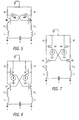
- FIG. 5 is a schematic diagram of the resonator of Figure 4 with an illustrative implementation of the negative resistors thereof.
- resistors R 1 and R 2 are disposed in series with the first and second inductors.
- the resistors R 1 and R 2 should be equal to the parasitic serial resistors R L1 and R L2 .
- First and second transistors Q 1 and Q 2 are connected in between the resistors R 1 and R 2 and the associated component, in the illustrative application, the first and second inductors L 1 and L 2 , respectively.
- the collector of Q 1 is connected to R 1 at a node A and the collector of Q 2 is connected to R 2 at a node B.
- a first voltage follower (unity-gain amplifier) 42 is connected between node A and the base of Q2.
- the second voltage follower 44 is connected between node B and the base of Q1.
- the first and second voltage followers 42 and 44 can be implemented by emitter followers as shown in Figure 6 below, source followers as shown in Figure 7 or other suitable circuit arrangement as will be appreciated by those of ordinary skill in the art.
- Figure 6 is a schematic diagram of the resonator of Figure 5 with a bipolar emitter follower implementation for the voltage followers thereof.
- the first follower 42 is implemented with a third bipolar transistor Q 3 having its base connected to node A, its collector connected to ground and its emitter connected to a first current source 46.
- the second follower 44 is implemented with a fourth bipolar transistor Q 4 having its base connected to node B, its collector connected to ground and its emitter connected to a second current source 48. While an NPN implementation is shown, those skilled in the art will appreciate that a PNP implementation may be employed as well.
- FIG. 7 is a schematic diagram of the resonator of Figure 5 with a MOSFET source follower implementation for the voltage followers thereof.
- n-channel MOSFETs M 1 and M 2 are used in place of the first and second transistors Q 1 and Q 2 of Figure 6 .
- the first follower 42 is implemented with a third MOSFET transistor M 3 having its gate connected to node A, its drain connected to ground and its source connected to the first current source 46.
- the second follower 44 is implemented with a fourth MOSFET transistor M 4 having its gate connected to node B, its drain connected to ground and its source connected to the second current source 48. While an n-channel implementation is shown, those skilled in the art will appreciate that a p-channel implementation may be employed as well.
- the inventive enhancement circuit 40 should cancel the effect of the inherent parasitic resistance and improve the Q factor of the components with which it is used.
Landscapes
- Amplifiers (AREA)
- Inductance-Capacitance Distribution Constants And Capacitance-Resistance Oscillators (AREA)
- Filters And Equalizers (AREA)
- Networks Using Active Elements (AREA)
- Paper (AREA)
Applications Claiming Priority (2)
| Application Number | Priority Date | Filing Date | Title |
|---|---|---|---|
| US10/864,158 US7202762B2 (en) | 2004-06-09 | 2004-06-09 | Q enhancement circuit and method |
| PCT/US2005/012300 WO2006001878A1 (en) | 2004-06-09 | 2005-04-11 | Q enhancement circuit and method |
Publications (2)
| Publication Number | Publication Date |
|---|---|
| EP1754308A1 EP1754308A1 (en) | 2007-02-21 |
| EP1754308B1 true EP1754308B1 (en) | 2008-09-03 |
Family
ID=34965205
Family Applications (1)
| Application Number | Title | Priority Date | Filing Date |
|---|---|---|---|
| EP05735127A Expired - Fee Related EP1754308B1 (en) | 2004-06-09 | 2005-04-11 | Q enhancement circuit and method |
Country Status (7)
| Country | Link |
|---|---|
| US (1) | US7202762B2 (ja) |
| EP (1) | EP1754308B1 (ja) |
| JP (1) | JP4659832B2 (ja) |
| KR (1) | KR100866235B1 (ja) |
| DE (1) | DE602005009526D1 (ja) |
| NO (1) | NO20070078L (ja) |
| WO (1) | WO2006001878A1 (ja) |
Families Citing this family (5)
| Publication number | Priority date | Publication date | Assignee | Title |
|---|---|---|---|---|
| US7884680B2 (en) * | 2008-06-30 | 2011-02-08 | Infineon Technologies Ag | Dynamically adjustable Q-factors |
| DE102009012767B4 (de) * | 2009-03-12 | 2013-05-23 | Texas Instruments Deutschland Gmbh | Geschaltete Spannungsversorgung mit Stromabtastung |
| US9124279B2 (en) | 2012-09-03 | 2015-09-01 | Tensorcom, Inc. | Method and apparatus for an active negative-capacitor circuit to cancel the input capacitance of comparators |
| RU2712784C1 (ru) * | 2019-02-04 | 2020-01-31 | Федеральное государственное бюджетное образовательное учреждение высшего образования "Ростовский государственный университет путей сообщения" (ФГБОУ ВО РГУПС) | Способ измерения добротности резонатора |
| US11047139B2 (en) | 2019-07-09 | 2021-06-29 | Schluter Systems L.P. | Veneer profile with fastening feature and related methods |
Family Cites Families (17)
| Publication number | Priority date | Publication date | Assignee | Title |
|---|---|---|---|---|
| GB2181914B (en) * | 1985-10-22 | 1989-09-20 | Plessey Co Plc | Frequency doubling oscillator and heterodyne circuit incorporating same |
| JP3381283B2 (ja) | 1991-12-24 | 2003-02-24 | 株式会社デンソー | 可変リアクタンス回路およびこれを用いた可変整合回路 |
| US5892425A (en) * | 1997-04-10 | 1999-04-06 | Virginia Tech Intellectual Properties, Inc. | Interwound center-tapped spiral inductor |
| JPH11330851A (ja) * | 1998-05-11 | 1999-11-30 | Matsushita Electric Ind Co Ltd | 発振器 |
| JP3923690B2 (ja) * | 1999-10-05 | 2007-06-06 | 株式会社東芝 | 電圧制御発振装置 |
| US6469586B1 (en) * | 2000-08-25 | 2002-10-22 | Sige Semiconductor Inc. | Low voltage voltage-controlled oscillator topology |
| US6681103B1 (en) * | 2000-08-25 | 2004-01-20 | Sige Semiconductor Inc. | On-chip image reject filter |
| US6778023B2 (en) | 2001-07-31 | 2004-08-17 | Nokia Corporation | Tunable filter and method of tuning a filter |
| US6680655B2 (en) * | 2001-08-01 | 2004-01-20 | Sige Semiconductor Inc. | Automatic gain control for a voltage controlled oscillator |
| JP2003045722A (ja) * | 2001-08-01 | 2003-02-14 | Sony Corp | インダクタ素子、および、インダクタ素子を用いた集積回路 |
| US6621331B2 (en) * | 2001-08-07 | 2003-09-16 | Hrl Laboratories, Llc | Variable negative resistance cell for bipolar integrated circuits |
| US6930562B2 (en) * | 2002-07-16 | 2005-08-16 | Matsushita Electric Industrial Co., Ltd. | Oscillation with multiple series circuits in parallel |
| US6650163B1 (en) * | 2002-08-08 | 2003-11-18 | International Business Machines Corporation | Clock generator for integrated circuit |
| JP4245391B2 (ja) * | 2003-03-27 | 2009-03-25 | 株式会社ルネサステクノロジ | 無線通信システムおよび通信用半導体集積回路 |
| US6970048B1 (en) * | 2003-12-12 | 2005-11-29 | National Semiconductor Corporation | Inductive-capacitive (LC) based quadrature voltage controlled oscillator (VCO) with deterministic quadrature signal phase relationship |
| US20050156681A1 (en) * | 2004-01-20 | 2005-07-21 | Koji Takinami | Voltage controlled oscillator |
| KR100615552B1 (ko) * | 2004-06-01 | 2006-08-25 | 학교법인 한국정보통신학원 | 직렬 교차 연결된 상보형 트랜지스터를 이용한 전압 제어발진기 및 이를 이용한 신호 송수신 장치 |
-
2004
- 2004-06-09 US US10/864,158 patent/US7202762B2/en not_active Expired - Fee Related
-
2005
- 2005-04-11 EP EP05735127A patent/EP1754308B1/en not_active Expired - Fee Related
- 2005-04-11 JP JP2007527230A patent/JP4659832B2/ja not_active Expired - Fee Related
- 2005-04-11 DE DE602005009526T patent/DE602005009526D1/de active Active
- 2005-04-11 WO PCT/US2005/012300 patent/WO2006001878A1/en not_active Application Discontinuation
- 2005-04-11 KR KR1020067025933A patent/KR100866235B1/ko not_active IP Right Cessation
-
2007
- 2007-01-05 NO NO20070078A patent/NO20070078L/no not_active Application Discontinuation
Also Published As
| Publication number | Publication date |
|---|---|
| DE602005009526D1 (de) | 2008-10-16 |
| KR100866235B1 (ko) | 2008-10-30 |
| US7202762B2 (en) | 2007-04-10 |
| KR20070014196A (ko) | 2007-01-31 |
| JP2008503178A (ja) | 2008-01-31 |
| US20050275490A1 (en) | 2005-12-15 |
| NO20070078L (no) | 2007-01-05 |
| WO2006001878A1 (en) | 2006-01-05 |
| EP1754308A1 (en) | 2007-02-21 |
| JP4659832B2 (ja) | 2011-03-30 |
Similar Documents
| Publication | Publication Date | Title |
|---|---|---|
| US7535323B2 (en) | Bulk acoustic wave filter with reduced nonlinear signal distortion | |
| EP1816742B1 (de) | Differenzverstärker und Funksystem mit Differenzverstärker | |
| JP3080723B2 (ja) | フィルタ回路及びフィルタ集積回路 | |
| US6922108B2 (en) | Active balun circuit for single-ended to differential RF signal conversion with enhanced common-mode rejection | |
| CN107026621B (zh) | 功率放大器系统和相关的偏置电路 | |
| EP1754308B1 (en) | Q enhancement circuit and method | |
| US20060290441A1 (en) | Quasi-Balun | |
| FI100751B (fi) | Pienikohinainen vahvistin | |
| EP1142107B1 (en) | Active differential to single-ended converter | |
| US9124251B2 (en) | Two stage source-follower based filter | |
| CN110022136B (zh) | 滤波器网络 | |
| JP3853604B2 (ja) | 周波数変換回路 | |
| US5099155A (en) | Active element filter network | |
| JP2007274179A (ja) | 同調回路及びこれに用いる可変利得減衰器 | |
| US10027305B1 (en) | Filter including non-magnetic frequency selective limiters | |
| EP1161792A1 (en) | Linearized transconductance cell | |
| JP3332657B2 (ja) | ミキサ回路 | |
| JP2639808B2 (ja) | アクテイブフイルタ | |
| WO2013088337A1 (en) | Low-noise electronic circuit simulating the behaviour of an inductance | |
| JP3300301B2 (ja) | 低域通過フィルタ | |
| EP1265357A1 (en) | Driver circuit | |
| JPH09148880A (ja) | 電子回路、これを用いたフィルタ装置及び無線装置 | |
| JP4761851B2 (ja) | 帰還形信号処理回路 | |
| CN114640310A (zh) | 一种振荡电路和一种压控振荡器 | |
| JP2007006302A (ja) | インピーダンス変換回路と、これを用いたハイパスフィルタ回路および周波数変換回路 |
Legal Events
| Date | Code | Title | Description |
|---|---|---|---|
| PUAI | Public reference made under article 153(3) epc to a published international application that has entered the european phase |
Free format text: ORIGINAL CODE: 0009012 |
|
| 17P | Request for examination filed |
Effective date: 20061114 |
|
| AK | Designated contracting states |
Kind code of ref document: A1 Designated state(s): DE FR SE |
|
| DAX | Request for extension of the european patent (deleted) | ||
| RBV | Designated contracting states (corrected) |
Designated state(s): DE FR SE |
|
| GRAP | Despatch of communication of intention to grant a patent |
Free format text: ORIGINAL CODE: EPIDOSNIGR1 |
|
| GRAS | Grant fee paid |
Free format text: ORIGINAL CODE: EPIDOSNIGR3 |
|
| GRAA | (expected) grant |
Free format text: ORIGINAL CODE: 0009210 |
|
| AK | Designated contracting states |
Kind code of ref document: B1 Designated state(s): DE FR SE |
|
| REF | Corresponds to: |
Ref document number: 602005009526 Country of ref document: DE Date of ref document: 20081016 Kind code of ref document: P |
|
| REG | Reference to a national code |
Ref country code: SE Ref legal event code: TRGR |
|
| PLBE | No opposition filed within time limit |
Free format text: ORIGINAL CODE: 0009261 |
|
| STAA | Information on the status of an ep patent application or granted ep patent |
Free format text: STATUS: NO OPPOSITION FILED WITHIN TIME LIMIT |
|
| 26N | No opposition filed |
Effective date: 20090604 |
|
| PGFP | Annual fee paid to national office [announced via postgrant information from national office to epo] |
Ref country code: DE Payment date: 20110406 Year of fee payment: 7 Ref country code: FR Payment date: 20110426 Year of fee payment: 7 Ref country code: SE Payment date: 20110412 Year of fee payment: 7 |
|
| REG | Reference to a national code |
Ref country code: SE Ref legal event code: EUG |
|
| REG | Reference to a national code |
Ref country code: FR Ref legal event code: ST Effective date: 20121228 |
|
| REG | Reference to a national code |
Ref country code: DE Ref legal event code: R119 Ref document number: 602005009526 Country of ref document: DE Effective date: 20121101 |
|
| PG25 | Lapsed in a contracting state [announced via postgrant information from national office to epo] |
Ref country code: FR Free format text: LAPSE BECAUSE OF NON-PAYMENT OF DUE FEES Effective date: 20120430 Ref country code: SE Free format text: LAPSE BECAUSE OF NON-PAYMENT OF DUE FEES Effective date: 20120412 |
|
| PG25 | Lapsed in a contracting state [announced via postgrant information from national office to epo] |
Ref country code: DE Free format text: LAPSE BECAUSE OF NON-PAYMENT OF DUE FEES Effective date: 20121101 |