EP1744204B1 - Liquid crystal display device and electronic apparatus - Google Patents
Liquid crystal display device and electronic apparatus Download PDFInfo
- Publication number
- EP1744204B1 EP1744204B1 EP06253718A EP06253718A EP1744204B1 EP 1744204 B1 EP1744204 B1 EP 1744204B1 EP 06253718 A EP06253718 A EP 06253718A EP 06253718 A EP06253718 A EP 06253718A EP 1744204 B1 EP1744204 B1 EP 1744204B1
- Authority
- EP
- European Patent Office
- Prior art keywords
- liquid crystal
- layer
- area
- electrode
- display device
- Prior art date
- Legal status (The legal status is an assumption and is not a legal conclusion. Google has not performed a legal analysis and makes no representation as to the accuracy of the status listed.)
- Expired - Fee Related
Links
Images


Classifications
-
- G—PHYSICS
- G02—OPTICS
- G02F—OPTICAL DEVICES OR ARRANGEMENTS FOR THE CONTROL OF LIGHT BY MODIFICATION OF THE OPTICAL PROPERTIES OF THE MEDIA OF THE ELEMENTS INVOLVED THEREIN; NON-LINEAR OPTICS; FREQUENCY-CHANGING OF LIGHT; OPTICAL LOGIC ELEMENTS; OPTICAL ANALOGUE/DIGITAL CONVERTERS
- G02F1/00—Devices or arrangements for the control of the intensity, colour, phase, polarisation or direction of light arriving from an independent light source, e.g. switching, gating or modulating; Non-linear optics
- G02F1/01—Devices or arrangements for the control of the intensity, colour, phase, polarisation or direction of light arriving from an independent light source, e.g. switching, gating or modulating; Non-linear optics for the control of the intensity, phase, polarisation or colour
- G02F1/13—Devices or arrangements for the control of the intensity, colour, phase, polarisation or direction of light arriving from an independent light source, e.g. switching, gating or modulating; Non-linear optics for the control of the intensity, phase, polarisation or colour based on liquid crystals, e.g. single liquid crystal display cells
- G02F1/133—Constructional arrangements; Operation of liquid crystal cells; Circuit arrangements
- G02F1/1333—Constructional arrangements; Manufacturing methods
- G02F1/1335—Structural association of cells with optical devices, e.g. polarisers or reflectors
- G02F1/133553—Reflecting elements
- G02F1/133555—Transflectors
-
- G—PHYSICS
- G02—OPTICS
- G02F—OPTICAL DEVICES OR ARRANGEMENTS FOR THE CONTROL OF LIGHT BY MODIFICATION OF THE OPTICAL PROPERTIES OF THE MEDIA OF THE ELEMENTS INVOLVED THEREIN; NON-LINEAR OPTICS; FREQUENCY-CHANGING OF LIGHT; OPTICAL LOGIC ELEMENTS; OPTICAL ANALOGUE/DIGITAL CONVERTERS
- G02F1/00—Devices or arrangements for the control of the intensity, colour, phase, polarisation or direction of light arriving from an independent light source, e.g. switching, gating or modulating; Non-linear optics
- G02F1/01—Devices or arrangements for the control of the intensity, colour, phase, polarisation or direction of light arriving from an independent light source, e.g. switching, gating or modulating; Non-linear optics for the control of the intensity, phase, polarisation or colour
- G02F1/13—Devices or arrangements for the control of the intensity, colour, phase, polarisation or direction of light arriving from an independent light source, e.g. switching, gating or modulating; Non-linear optics for the control of the intensity, phase, polarisation or colour based on liquid crystals, e.g. single liquid crystal display cells
- G02F1/133—Constructional arrangements; Operation of liquid crystal cells; Circuit arrangements
- G02F1/1333—Constructional arrangements; Manufacturing methods
- G02F1/1335—Structural association of cells with optical devices, e.g. polarisers or reflectors
-
- G—PHYSICS
- G02—OPTICS
- G02F—OPTICAL DEVICES OR ARRANGEMENTS FOR THE CONTROL OF LIGHT BY MODIFICATION OF THE OPTICAL PROPERTIES OF THE MEDIA OF THE ELEMENTS INVOLVED THEREIN; NON-LINEAR OPTICS; FREQUENCY-CHANGING OF LIGHT; OPTICAL LOGIC ELEMENTS; OPTICAL ANALOGUE/DIGITAL CONVERTERS
- G02F1/00—Devices or arrangements for the control of the intensity, colour, phase, polarisation or direction of light arriving from an independent light source, e.g. switching, gating or modulating; Non-linear optics
- G02F1/01—Devices or arrangements for the control of the intensity, colour, phase, polarisation or direction of light arriving from an independent light source, e.g. switching, gating or modulating; Non-linear optics for the control of the intensity, phase, polarisation or colour
- G02F1/13—Devices or arrangements for the control of the intensity, colour, phase, polarisation or direction of light arriving from an independent light source, e.g. switching, gating or modulating; Non-linear optics for the control of the intensity, phase, polarisation or colour based on liquid crystals, e.g. single liquid crystal display cells
- G02F1/133—Constructional arrangements; Operation of liquid crystal cells; Circuit arrangements
- G02F1/1333—Constructional arrangements; Manufacturing methods
- G02F1/1343—Electrodes
- G02F1/134309—Electrodes characterised by their geometrical arrangement
- G02F1/134363—Electrodes characterised by their geometrical arrangement for applying an electric field parallel to the substrate, i.e. in-plane switching [IPS]
-
- G—PHYSICS
- G02—OPTICS
- G02F—OPTICAL DEVICES OR ARRANGEMENTS FOR THE CONTROL OF LIGHT BY MODIFICATION OF THE OPTICAL PROPERTIES OF THE MEDIA OF THE ELEMENTS INVOLVED THEREIN; NON-LINEAR OPTICS; FREQUENCY-CHANGING OF LIGHT; OPTICAL LOGIC ELEMENTS; OPTICAL ANALOGUE/DIGITAL CONVERTERS
- G02F1/00—Devices or arrangements for the control of the intensity, colour, phase, polarisation or direction of light arriving from an independent light source, e.g. switching, gating or modulating; Non-linear optics
- G02F1/01—Devices or arrangements for the control of the intensity, colour, phase, polarisation or direction of light arriving from an independent light source, e.g. switching, gating or modulating; Non-linear optics for the control of the intensity, phase, polarisation or colour
- G02F1/13—Devices or arrangements for the control of the intensity, colour, phase, polarisation or direction of light arriving from an independent light source, e.g. switching, gating or modulating; Non-linear optics for the control of the intensity, phase, polarisation or colour based on liquid crystals, e.g. single liquid crystal display cells
- G02F1/133—Constructional arrangements; Operation of liquid crystal cells; Circuit arrangements
- G02F1/1333—Constructional arrangements; Manufacturing methods
- G02F1/133371—Cells with varying thickness of the liquid crystal layer
-
- G—PHYSICS
- G02—OPTICS
- G02F—OPTICAL DEVICES OR ARRANGEMENTS FOR THE CONTROL OF LIGHT BY MODIFICATION OF THE OPTICAL PROPERTIES OF THE MEDIA OF THE ELEMENTS INVOLVED THEREIN; NON-LINEAR OPTICS; FREQUENCY-CHANGING OF LIGHT; OPTICAL LOGIC ELEMENTS; OPTICAL ANALOGUE/DIGITAL CONVERTERS
- G02F1/00—Devices or arrangements for the control of the intensity, colour, phase, polarisation or direction of light arriving from an independent light source, e.g. switching, gating or modulating; Non-linear optics
- G02F1/01—Devices or arrangements for the control of the intensity, colour, phase, polarisation or direction of light arriving from an independent light source, e.g. switching, gating or modulating; Non-linear optics for the control of the intensity, phase, polarisation or colour
- G02F1/13—Devices or arrangements for the control of the intensity, colour, phase, polarisation or direction of light arriving from an independent light source, e.g. switching, gating or modulating; Non-linear optics for the control of the intensity, phase, polarisation or colour based on liquid crystals, e.g. single liquid crystal display cells
- G02F1/133—Constructional arrangements; Operation of liquid crystal cells; Circuit arrangements
- G02F1/1333—Constructional arrangements; Manufacturing methods
- G02F1/1335—Structural association of cells with optical devices, e.g. polarisers or reflectors
- G02F1/13363—Birefringent elements, e.g. for optical compensation
- G02F1/133631—Birefringent elements, e.g. for optical compensation with a spatial distribution of the retardation value
-
- G—PHYSICS
- G02—OPTICS
- G02F—OPTICAL DEVICES OR ARRANGEMENTS FOR THE CONTROL OF LIGHT BY MODIFICATION OF THE OPTICAL PROPERTIES OF THE MEDIA OF THE ELEMENTS INVOLVED THEREIN; NON-LINEAR OPTICS; FREQUENCY-CHANGING OF LIGHT; OPTICAL LOGIC ELEMENTS; OPTICAL ANALOGUE/DIGITAL CONVERTERS
- G02F1/00—Devices or arrangements for the control of the intensity, colour, phase, polarisation or direction of light arriving from an independent light source, e.g. switching, gating or modulating; Non-linear optics
- G02F1/01—Devices or arrangements for the control of the intensity, colour, phase, polarisation or direction of light arriving from an independent light source, e.g. switching, gating or modulating; Non-linear optics for the control of the intensity, phase, polarisation or colour
- G02F1/13—Devices or arrangements for the control of the intensity, colour, phase, polarisation or direction of light arriving from an independent light source, e.g. switching, gating or modulating; Non-linear optics for the control of the intensity, phase, polarisation or colour based on liquid crystals, e.g. single liquid crystal display cells
- G02F1/133—Constructional arrangements; Operation of liquid crystal cells; Circuit arrangements
- G02F1/1333—Constructional arrangements; Manufacturing methods
- G02F1/1335—Structural association of cells with optical devices, e.g. polarisers or reflectors
- G02F1/13363—Birefringent elements, e.g. for optical compensation
- G02F1/133638—Waveplates, i.e. plates with a retardation value of lambda/n
Definitions
- incident light from the second substrate can be converted into wide-band circular polarized light by the use of the liquid crystal layer and the retardation layer formed on the side of the second substrate opposed to the liquid crystal layer. Accordingly, it is possible to provide reflective black display with small color, thereby embodying reflective display with high contrast.
- the first electrode and the second electrode may have a plurality of band-shaped electrodes. That is, an electric field (transverse electric field) generating configuration that the first electrode and the second electrode are two-dimensionally adjacent and opposed to each other in the same plane can be employed.
- an electrode structure that the first electrode and the second electrode are both formed in a pectinated shape as seen two dimensionally and the band-shaped electrodes constituting the pectinated portions thereof are alternately arranged can be employed.
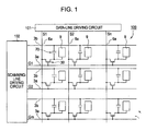
- Fig. 1 is a circuit diagram illustrating a plurality of sub pixel areas arranged in a matrix shape in the liquid crystal display device according to the first embodiment.
- Fig. 2A is a plan view illustrating a sub pixel area in the liquid crystal display device 100 and Fig. 2B is a diagram illustrating arrangement of optical axes in Fig. 2A .
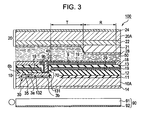
- Fig. 3 is a partially sectional view taken along Line III-III of Fig. 2A .
- the common electrode 19 is formed to cover the reflective layer 29 partially formed in the sub pixel area shown in Fig. 2A .
- the common electrode 19 is a conductive film made of a transparent conductive material such as ITO (Indium Tin Oxide), and the reflective layer 29 is formed out of a reflective metal film such as aluminum or silver, or a dielectric laminated film (dielectric mirror) formed by stacking dielectric films (SiO 2 and TiO 2 ) having different refractive indexes.
- a first interlayer insulating layer 12 is formed to cover the semiconductor layer 35, the source electrode 6b, the drain electrode 132, and the capacitor electrode 131, and the reflective layer 29 is formed on a part of the first interlayer insulating layer 12.
- the common electrode 19 made of a transparent material such as ITO is formed to cover the reflective layer 29 and the first interlayer insulating layer 12.
- the thickness of the liquid crystal layer (cell gap) in the transmissive display area T is 3.5 ⁇ m and the thickness of the liquid crystal layer in the reflective display area R is 1.4 ⁇ m (that is, the thickness of the retardation layer 21 is 2.1 ⁇ m).
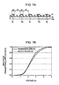
- the chromaticity of the first color material area is set to be greater than the chromaticity of the second color material area, it is possible to prevent the chromaticity of display light from varying in the transmissive display area T where the display light passes through the color filter 22 only one time and the reflective display area R where the display light passes through the color filter 22 two times, thereby making visual quality constant in the transmissive display and the reflective display.
- the reflective layer 29 has been disposed on the side of the TFT array substrate 10 in the second embodiment, the reflective layer 29 may be disposed on the side of the counter substrate 20 and the retardation layer 21 may be disposed on the side of the TFT array substrate. In this case, the same characteristic can be obtained.
- the stack order may be changed so as to stack the retardation layer 21 and the resin layer 23 in the area on the color filter 22 corresponding to the reflective display area R in this order.
- liquid crystal display device 500 according to the fifth embodiment having the above-mentioned structure similarly to the liquid crystal display device 400 according to the fourth embodiment, since the unevenness resulting from the opening 22a is made flat by the planarization layer 25 and then the retardation layer 21 is formed thereon, it is possible to easily form the retardation layer 21 having a desired phase difference, thereby obtaining the high-contrast display.
- Fig. 9 is a perspective view illustrating a mobile phone as an example of an electronic apparatus having the liquid crystal display device according to the invention as a display unit.
- the mobile phone 1300 has the liquid crystal display device according to the invention as a small-sized display unit 1301 and includes a plurality of operation buttons 1302, an earpiece 1303, and a mouthpiece 1304.
Landscapes
- Physics & Mathematics (AREA)
- Nonlinear Science (AREA)
- Mathematical Physics (AREA)
- Chemical & Material Sciences (AREA)
- Crystallography & Structural Chemistry (AREA)
- General Physics & Mathematics (AREA)
- Optics & Photonics (AREA)
- Geometry (AREA)
- Liquid Crystal (AREA)
Applications Claiming Priority (2)
| Application Number | Priority Date | Filing Date | Title |
|---|---|---|---|
| JP2005207015 | 2005-07-15 | ||
| JP2006016017A JP4039444B2 (ja) | 2005-07-15 | 2006-01-25 | 液晶表示装置及び電子機器 |
Publications (2)
| Publication Number | Publication Date |
|---|---|
| EP1744204A1 EP1744204A1 (en) | 2007-01-17 |
| EP1744204B1 true EP1744204B1 (en) | 2010-03-03 |
Family
ID=36954725
Family Applications (1)
| Application Number | Title | Priority Date | Filing Date |
|---|---|---|---|
| EP06253718A Expired - Fee Related EP1744204B1 (en) | 2005-07-15 | 2006-07-14 | Liquid crystal display device and electronic apparatus |
Country Status (6)
| Country | Link |
|---|---|
| US (1) | US7602463B2 (ja) |
| EP (1) | EP1744204B1 (ja) |
| JP (1) | JP4039444B2 (ja) |
| KR (1) | KR100760745B1 (ja) |
| DE (1) | DE602006012587D1 (ja) |
| TW (1) | TWI346229B (ja) |
Families Citing this family (49)
| Publication number | Priority date | Publication date | Assignee | Title |
|---|---|---|---|---|
| US7125356B2 (en) | 2001-11-06 | 2006-10-24 | Borgwarner Inc. | Tension-reducing random sprocket |
| KR101189275B1 (ko) | 2005-08-26 | 2012-10-09 | 삼성디스플레이 주식회사 | 박막 트랜지스터 표시판 및 그 제조 방법 |
| US20120236241A1 (en) * | 2005-09-15 | 2012-09-20 | Ong Hiap L | Liquid Crystal Displays Having Pixels with Embedded Fringe Field Amplifiers |
| DE102006057333B4 (de) | 2005-12-30 | 2010-01-28 | Lg Display Co., Ltd. | IPS-Flüssigkristallanzeigevorrichtung |
| TWI362550B (en) * | 2007-06-21 | 2012-04-21 | Ether Precision Inc | The method for manufacturing the image captures unit |
| EP2085813B1 (en) | 2006-10-18 | 2014-01-01 | Sharp Kabushiki Kaisha | Liquid crystal display and method for manufacturing liquid crystal display |
| US8421967B2 (en) | 2006-12-14 | 2013-04-16 | Sharp Kabushiki Kaisha | Liquid crystal display device and process for producing liquid crystal display device |
| JP4943454B2 (ja) | 2007-01-24 | 2012-05-30 | シャープ株式会社 | 液晶表示装置 |
| KR100885184B1 (ko) | 2007-01-30 | 2009-02-23 | 삼성전자주식회사 | 전기장 및 자기장에 의해 독립적으로 제어될 수 있는 저항특성을 갖는 메모리 장치 및 그 동작 방법 |
| JP4329828B2 (ja) * | 2007-02-26 | 2009-09-09 | エプソンイメージングデバイス株式会社 | 液晶表示装置 |
| JP4529984B2 (ja) * | 2007-02-26 | 2010-08-25 | エプソンイメージングデバイス株式会社 | 液晶装置及び電子機器 |
| JP4337893B2 (ja) * | 2007-03-12 | 2009-09-30 | エプソンイメージングデバイス株式会社 | 液晶装置及び電子機器 |
| US8619225B2 (en) * | 2007-03-28 | 2013-12-31 | Japan Display West Inc. | Liquid crystal device with pixel electrode under the common electrode and thinner than drain electrode, method of manufacturing liquid crystal device, and electronic apparatus |
| US8018554B2 (en) | 2007-03-28 | 2011-09-13 | Sony Corporation | Liquid crystal display device with internal retardation layer at reflection region and electronic apparatus |
| JP5184517B2 (ja) | 2007-04-13 | 2013-04-17 | シャープ株式会社 | 液晶表示装置 |
| JP2008275761A (ja) * | 2007-04-26 | 2008-11-13 | Hitachi Displays Ltd | 液晶表示装置とその製造方法 |
| JP2008299312A (ja) * | 2007-05-01 | 2008-12-11 | Epson Imaging Devices Corp | 液晶表示装置および電子機器 |
| JP2008275966A (ja) | 2007-05-01 | 2008-11-13 | Epson Imaging Devices Corp | 液晶表示装置および電子機器 |
| JP4900072B2 (ja) * | 2007-06-14 | 2012-03-21 | ソニー株式会社 | 液晶装置および電子機器 |
| JP4900073B2 (ja) * | 2007-06-14 | 2012-03-21 | ソニー株式会社 | 液晶装置および電子機器 |
| WO2009001508A1 (ja) | 2007-06-26 | 2008-12-31 | Sharp Kabushiki Kaisha | 液晶表示装置、及び液晶表示装置の製造方法 |
| JP4960164B2 (ja) * | 2007-07-20 | 2012-06-27 | 株式会社ジャパンディスプレイイースト | 液晶表示装置 |
| JP5376417B2 (ja) * | 2007-07-30 | 2013-12-25 | 株式会社ジャパンディスプレイ | 半透過型液晶表示パネル |
| JP5154298B2 (ja) * | 2007-08-01 | 2013-02-27 | 株式会社ジャパンディスプレイウェスト | 液晶表示パネル、その製造方法 |
| JP4799505B2 (ja) | 2007-08-03 | 2011-10-26 | 株式会社 日立ディスプレイズ | 液晶表示装置 |
| JP5472773B2 (ja) * | 2007-08-30 | 2014-04-16 | Nltテクノロジー株式会社 | 半透過型液晶表示装置 |
| JP5215617B2 (ja) * | 2007-09-04 | 2013-06-19 | 株式会社ジャパンディスプレイイースト | 液晶表示装置 |
| JP5309512B2 (ja) * | 2007-09-20 | 2013-10-09 | 大日本印刷株式会社 | 半透過型ips液晶表示装置用カラーフィルタの製造方法 |
| JP5334012B2 (ja) * | 2007-09-20 | 2013-11-06 | 株式会社ジャパンディスプレイ | 半透過型液晶表示パネル及び電子機器 |
| US8430775B2 (en) | 2007-09-28 | 2013-04-30 | Borgwarner Inc. | Multiple tension reducing sprockets in a chain and sprocket system |
| JP5291913B2 (ja) * | 2007-10-16 | 2013-09-18 | 株式会社ジャパンディスプレイウェスト | 半透過型液晶表示パネルの製造方法 |
| JP2009103815A (ja) * | 2007-10-22 | 2009-05-14 | Dainippon Printing Co Ltd | 半透過型液晶表示装置、位相変調素子、露光方法、及び位相変調素子の製造方法 |
| JP2009103775A (ja) * | 2007-10-22 | 2009-05-14 | Hitachi Displays Ltd | 液晶表示装置 |
| JP4678031B2 (ja) * | 2008-01-11 | 2011-04-27 | ソニー株式会社 | 液晶装置および電子機器 |
| KR100922055B1 (ko) * | 2008-02-19 | 2009-10-21 | 삼성모바일디스플레이주식회사 | 액정표시장치 |
| JP2009237019A (ja) * | 2008-03-26 | 2009-10-15 | Seiko Epson Corp | 液晶表示装置及び電子機器 |
| CN101910920B (zh) * | 2008-03-31 | 2012-06-20 | 凸版印刷株式会社 | 相位差基板、半透射型液晶显示装置及相位差基板的制造方法 |
| JP2009258332A (ja) | 2008-04-16 | 2009-11-05 | Seiko Epson Corp | 液晶表示装置、電子機器 |
| JP5273368B2 (ja) * | 2008-11-26 | 2013-08-28 | 株式会社ジャパンディスプレイ | 液晶表示装置 |
| KR101250319B1 (ko) * | 2009-10-06 | 2013-04-03 | 엘지디스플레이 주식회사 | 프린지 필드 스위칭 모드 액정표시장치용 어레이 기판과 그 제조방법 |
| US8884509B2 (en) * | 2011-03-02 | 2014-11-11 | Semiconductor Energy Laboratory Co., Ltd. | Optical device, display device, and lighting device |
| US20130200377A1 (en) * | 2012-02-06 | 2013-08-08 | Shenzhen China Star Optoelectronics Technology Co. Ltd | Thin film transistor array substrate and method for manufacturing the same |
| US9366922B2 (en) * | 2012-02-07 | 2016-06-14 | Shenzhen China Star Optoelectronics Technology Co., Ltd. | Thin film transistor array and method for manufacturing the same |
| US20140152922A1 (en) * | 2012-12-05 | 2014-06-05 | Samsung Display Co., Ltd. | Liquid crystal display and method of manufacturing the same |
| KR102261760B1 (ko) | 2014-07-29 | 2021-06-07 | 삼성디스플레이 주식회사 | 박막 트랜지스터 표시판 및 그 제조 방법 |
| KR102356827B1 (ko) * | 2015-03-04 | 2022-02-03 | 삼성디스플레이 주식회사 | 박막 트랜지스터 기판 및 그 제조 방법 |
| CN108368929B (zh) | 2015-12-09 | 2021-03-09 | 博格华纳公司 | 非普遍阶次随机链轮 |
| KR102469294B1 (ko) * | 2016-02-01 | 2022-11-23 | 삼성디스플레이 주식회사 | 유기 발광 표시 장치 |
| CN113495380B (zh) * | 2020-03-18 | 2023-12-01 | 瀚宇彩晶股份有限公司 | 反射式液晶显示面板 |
Family Cites Families (17)
| Publication number | Priority date | Publication date | Assignee | Title |
|---|---|---|---|---|
| JP3936126B2 (ja) * | 2000-08-30 | 2007-06-27 | シャープ株式会社 | 透過反射両用型液晶表示装置 |
| JP2005501293A (ja) * | 2001-08-29 | 2005-01-13 | コーニンクレッカ フィリップス エレクトロニクス エヌ ヴィ | 半透過型液晶ディスプレイにおける配列 |
| JP3873869B2 (ja) * | 2002-02-26 | 2007-01-31 | ソニー株式会社 | 液晶表示装置及びその製造方法 |
| JP2004004642A (ja) * | 2002-04-01 | 2004-01-08 | Nitto Denko Corp | 光学フィルムおよび画像表示装置 |
| JP4117148B2 (ja) * | 2002-05-24 | 2008-07-16 | 日本電気株式会社 | 半透過型液晶表示装置 |
| JP4078967B2 (ja) | 2002-12-11 | 2008-04-23 | セイコーエプソン株式会社 | 半透過型液晶表示装置 |
| JP4284221B2 (ja) * | 2003-03-31 | 2009-06-24 | 富士フイルム株式会社 | 液晶表示装置 |
| US20060203158A1 (en) * | 2003-04-08 | 2006-09-14 | Parri Owain L | Compensated lcd of the ips mode |
| JP2005031621A (ja) * | 2003-06-16 | 2005-02-03 | Nitto Denko Corp | 光学フィルム、偏光光学フィルムおよび画像表示装置 |
| JP4082683B2 (ja) * | 2003-09-29 | 2008-04-30 | 株式会社 日立ディスプレイズ | 半透過型液晶表示装置 |
| KR101014376B1 (ko) * | 2003-12-30 | 2011-02-15 | 엘지디스플레이 주식회사 | 위상차 필름을 포함하는 반투과형 액정 표시장치 |
| JP4223992B2 (ja) * | 2004-05-25 | 2009-02-12 | 株式会社 日立ディスプレイズ | 液晶表示装置 |
| WO2006010431A1 (en) | 2004-07-28 | 2006-02-02 | Merck Patent Gmbh | Transflective lcd comprising a patterned retardation film |
| JP4496874B2 (ja) * | 2004-07-29 | 2010-07-07 | Nec液晶テクノロジー株式会社 | 半透過型液晶表示装置、及びそれを搭載した電子機器 |
| KR101217945B1 (ko) | 2004-11-12 | 2013-01-02 | 메르크 파텐트 게엠베하 | 트랜스플렉티브 ips 액정 디스플레이 |
| JP4816862B2 (ja) * | 2004-12-16 | 2011-11-16 | ソニー株式会社 | 液晶表示装置 |
| JP2006292847A (ja) * | 2005-04-06 | 2006-10-26 | Toshiba Matsushita Display Technology Co Ltd | 液晶表示装置 |
-
2006
- 2006-01-25 JP JP2006016017A patent/JP4039444B2/ja not_active Expired - Fee Related
- 2006-07-13 US US11/485,382 patent/US7602463B2/en not_active Expired - Fee Related
- 2006-07-13 TW TW095125718A patent/TWI346229B/zh not_active IP Right Cessation
- 2006-07-14 DE DE602006012587T patent/DE602006012587D1/de active Active
- 2006-07-14 EP EP06253718A patent/EP1744204B1/en not_active Expired - Fee Related
- 2006-07-14 KR KR1020060066459A patent/KR100760745B1/ko active IP Right Grant
Also Published As
| Publication number | Publication date |
|---|---|
| JP4039444B2 (ja) | 2008-01-30 |
| EP1744204A1 (en) | 2007-01-17 |
| JP2007047732A (ja) | 2007-02-22 |
| US7602463B2 (en) | 2009-10-13 |
| TW200706980A (en) | 2007-02-16 |
| DE602006012587D1 (de) | 2010-04-15 |
| TWI346229B (en) | 2011-08-01 |
| KR100760745B1 (ko) | 2007-09-21 |
| US20070013773A1 (en) | 2007-01-18 |
| KR20070009475A (ko) | 2007-01-18 |
Similar Documents
| Publication | Publication Date | Title |
|---|---|---|
| EP1744204B1 (en) | Liquid crystal display device and electronic apparatus | |
| EP1744205B1 (en) | Liquid crystal display device and electronic apparatus | |
| KR100849343B1 (ko) | 액정 표시 장치, 액정 표시 장치의 제조 방법 및 전자 기기 | |
| JP4249544B2 (ja) | 液晶表示装置、及び電子機器 | |
| JP3807405B2 (ja) | 液晶表示装置、及び電子機器 | |
| US20090268140A1 (en) | Liquid crystal display device and electronic apparatus | |
| US7663716B2 (en) | Liquid crystal display device and electronic apparatus | |
| JP2007017943A (ja) | 液晶装置及び電子機器 | |
| JP2004240177A (ja) | 液晶表示装置および電子機器 | |
| JP4432371B2 (ja) | 液晶表示装置、及び電子機器 | |
| US7499138B2 (en) | Panel and a liquid crystal display including the panel | |
| JP2007334085A (ja) | 液晶表示装置、及び電子機器 | |
| JP4379081B2 (ja) | 液晶表示装置および電子機器 | |
| JP4830468B2 (ja) | 液晶表示パネル | |
| JP4438377B2 (ja) | 液晶表示装置、及び電子機器 | |
| JP4407234B2 (ja) | 液晶表示装置および電子機器 | |
| JP4483851B2 (ja) | 液晶表示装置及び電子機器 | |
| JP2007011410A (ja) | 液晶表示装置及び電子機器 | |
| JP2007018014A (ja) | 液晶表示装置及び電子機器 | |
| JP4249776B2 (ja) | 液晶表示装置、及び電子機器 | |
| JP2005031437A (ja) | 液晶表示装置および電子機器 | |
| JP2008268632A (ja) | 液晶装置及び電子機器 | |
| JP2007052455A (ja) | 液晶表示装置、及び電子機器 | |
| JP2007034331A (ja) | 液晶表示装置の製造方法 |
Legal Events
| Date | Code | Title | Description |
|---|---|---|---|
| PUAI | Public reference made under article 153(3) epc to a published international application that has entered the european phase |
Free format text: ORIGINAL CODE: 0009012 |
|
| AK | Designated contracting states |
Kind code of ref document: A1 Designated state(s): AT BE BG CH CY CZ DE DK EE ES FI FR GB GR HU IE IS IT LI LT LU LV MC NL PL PT RO SE SI SK TR |
|
| AX | Request for extension of the european patent |
Extension state: AL BA HR MK YU |
|
| RAP1 | Party data changed (applicant data changed or rights of an application transferred) |
Owner name: EPSON IMAGING DEVICES CORPORATION |
|
| RAP1 | Party data changed (applicant data changed or rights of an application transferred) |
Owner name: EPSON IMAGING DEVICES CORPORATION |
|
| 17P | Request for examination filed |
Effective date: 20070611 |
|
| 17Q | First examination report despatched |
Effective date: 20070705 |
|
| AKX | Designation fees paid |
Designated state(s): DE FR GB |
|
| GRAP | Despatch of communication of intention to grant a patent |
Free format text: ORIGINAL CODE: EPIDOSNIGR1 |
|
| RIN1 | Information on inventor provided before grant (corrected) |
Inventor name: TSUCHIYA, HITOSHI Inventor name: MATSUSHIMA, TOSHIHARU |
|
| GRAS | Grant fee paid |
Free format text: ORIGINAL CODE: EPIDOSNIGR3 |
|
| GRAA | (expected) grant |
Free format text: ORIGINAL CODE: 0009210 |
|
| AK | Designated contracting states |
Kind code of ref document: B1 Designated state(s): DE FR GB |
|
| REG | Reference to a national code |
Ref country code: GB Ref legal event code: FG4D |
|
| REF | Corresponds to: |
Ref document number: 602006012587 Country of ref document: DE Date of ref document: 20100415 Kind code of ref document: P |
|
| REG | Reference to a national code |
Ref country code: GB Ref legal event code: 732E Free format text: REGISTERED BETWEEN 20100715 AND 20100721 |
|
| REG | Reference to a national code |
Ref country code: FR Ref legal event code: TP |
|
| PLBE | No opposition filed within time limit |
Free format text: ORIGINAL CODE: 0009261 |
|
| STAA | Information on the status of an ep patent application or granted ep patent |
Free format text: STATUS: NO OPPOSITION FILED WITHIN TIME LIMIT |
|
| 26N | No opposition filed |
Effective date: 20101206 |
|
| REG | Reference to a national code |
Ref country code: DE Ref legal event code: R082 Ref document number: 602006012587 Country of ref document: DE Representative=s name: MITSCHERLICH & PARTNER PATENT- UND RECHTSANWAE, DE |
|
| REG | Reference to a national code |
Ref country code: DE Ref legal event code: R081 Ref document number: 602006012587 Country of ref document: DE Owner name: JAPAN DISPLAY WEST INC., JP Free format text: FORMER OWNER: SONY CORP., TOKIO/TOKYO, JP Effective date: 20130521 Ref country code: DE Ref legal event code: R082 Ref document number: 602006012587 Country of ref document: DE Representative=s name: MITSCHERLICH & PARTNER PATENT- UND RECHTSANWAE, DE Effective date: 20130521 Ref country code: DE Ref legal event code: R081 Ref document number: 602006012587 Country of ref document: DE Owner name: JAPAN DISPLAY WEST INC., OGAWA, JP Free format text: FORMER OWNER: SONY CORPORATION, TOKIO/TOKYO, JP Effective date: 20130521 Ref country code: DE Ref legal event code: R082 Ref document number: 602006012587 Country of ref document: DE Representative=s name: MITSCHERLICH, PATENT- UND RECHTSANWAELTE, PART, DE Effective date: 20130521 Ref country code: DE Ref legal event code: R082 Ref document number: 602006012587 Country of ref document: DE Representative=s name: MITSCHERLICH, PATENT- UND RECHTSANWAELTE PARTM, DE Effective date: 20130521 |
|
| REG | Reference to a national code |
Ref country code: FR Ref legal event code: TP Owner name: JAPAN DISPLAY WEST INC., JP Effective date: 20130619 |
|
| REG | Reference to a national code |
Ref country code: GB Ref legal event code: 732E Free format text: REGISTERED BETWEEN 20130627 AND 20130703 |
|
| REG | Reference to a national code |
Ref country code: FR Ref legal event code: PLFP Year of fee payment: 11 |
|
| REG | Reference to a national code |
Ref country code: FR Ref legal event code: PLFP Year of fee payment: 12 |
|
| REG | Reference to a national code |
Ref country code: FR Ref legal event code: PLFP Year of fee payment: 13 |
|
| PGFP | Annual fee paid to national office [announced via postgrant information from national office to epo] |
Ref country code: DE Payment date: 20180723 Year of fee payment: 13 Ref country code: FR Payment date: 20180725 Year of fee payment: 13 |
|
| PGFP | Annual fee paid to national office [announced via postgrant information from national office to epo] |
Ref country code: GB Payment date: 20180719 Year of fee payment: 13 |
|
| REG | Reference to a national code |
Ref country code: DE Ref legal event code: R119 Ref document number: 602006012587 Country of ref document: DE |
|
| GBPC | Gb: european patent ceased through non-payment of renewal fee |
Effective date: 20190714 |
|
| PG25 | Lapsed in a contracting state [announced via postgrant information from national office to epo] |
Ref country code: DE Free format text: LAPSE BECAUSE OF NON-PAYMENT OF DUE FEES Effective date: 20200201 Ref country code: GB Free format text: LAPSE BECAUSE OF NON-PAYMENT OF DUE FEES Effective date: 20190714 |
|
| PG25 | Lapsed in a contracting state [announced via postgrant information from national office to epo] |
Ref country code: FR Free format text: LAPSE BECAUSE OF NON-PAYMENT OF DUE FEES Effective date: 20190731 |