EP1716458B1 - Illumination system for a microlithographic projection exposure apparatus - Google Patents
Illumination system for a microlithographic projection exposure apparatus Download PDFInfo
- Publication number
- EP1716458B1 EP1716458B1 EP05707395A EP05707395A EP1716458B1 EP 1716458 B1 EP1716458 B1 EP 1716458B1 EP 05707395 A EP05707395 A EP 05707395A EP 05707395 A EP05707395 A EP 05707395A EP 1716458 B1 EP1716458 B1 EP 1716458B1
- Authority
- EP
- European Patent Office
- Prior art keywords
- lenses
- illumination system
- micro
- optical raster
- raster element
- Prior art date
- Legal status (The legal status is an assumption and is not a legal conclusion. Google has not performed a legal analysis and makes no representation as to the accuracy of the status listed.)
- Expired - Lifetime
Links
- 238000005286 illumination Methods 0.000 title claims abstract description 49
- 230000003287 optical effect Effects 0.000 claims abstract description 124
- 210000001747 pupil Anatomy 0.000 claims abstract description 23
- 238000004519 manufacturing process Methods 0.000 claims description 6
- 239000000758 substrate Substances 0.000 claims description 5
- 230000004907 flux Effects 0.000 abstract description 23
- 238000009826 distribution Methods 0.000 description 69
- 239000000306 component Substances 0.000 description 45
- 230000000694 effects Effects 0.000 description 14
- 229920002120 photoresistant polymer Polymers 0.000 description 12
- 238000013139 quantization Methods 0.000 description 8
- 238000003491 array Methods 0.000 description 7
- 230000000873 masking effect Effects 0.000 description 6
- 238000000034 method Methods 0.000 description 4
- 230000008569 process Effects 0.000 description 4
- 230000010287 polarization Effects 0.000 description 3
- 230000008901 benefit Effects 0.000 description 2
- 238000010276 construction Methods 0.000 description 2
- 238000000609 electron-beam lithography Methods 0.000 description 2
- 238000005516 engineering process Methods 0.000 description 2
- 239000011521 glass Substances 0.000 description 2
- 239000000463 material Substances 0.000 description 2
- 238000001393 microlithography Methods 0.000 description 2
- 239000010409 thin film Substances 0.000 description 2
- XUIMIQQOPSSXEZ-UHFFFAOYSA-N Silicon Chemical compound [Si] XUIMIQQOPSSXEZ-UHFFFAOYSA-N 0.000 description 1
- 230000002411 adverse Effects 0.000 description 1
- 230000001427 coherent effect Effects 0.000 description 1
- 238000005530 etching Methods 0.000 description 1
- 238000003384 imaging method Methods 0.000 description 1
- 230000006872 improvement Effects 0.000 description 1
- 230000010354 integration Effects 0.000 description 1
- 239000004973 liquid crystal related substance Substances 0.000 description 1
- 238000000206 photolithography Methods 0.000 description 1
- 238000013404 process transfer Methods 0.000 description 1
- 230000005855 radiation Effects 0.000 description 1
- 230000009467 reduction Effects 0.000 description 1
- 229910052710 silicon Inorganic materials 0.000 description 1
- 239000010703 silicon Substances 0.000 description 1
- 230000003595 spectral effect Effects 0.000 description 1
Images


Classifications
-
- G—PHYSICS
- G03—PHOTOGRAPHY; CINEMATOGRAPHY; ANALOGOUS TECHNIQUES USING WAVES OTHER THAN OPTICAL WAVES; ELECTROGRAPHY; HOLOGRAPHY
- G03F—PHOTOMECHANICAL PRODUCTION OF TEXTURED OR PATTERNED SURFACES, e.g. FOR PRINTING, FOR PROCESSING OF SEMICONDUCTOR DEVICES; MATERIALS THEREFOR; ORIGINALS THEREFOR; APPARATUS SPECIALLY ADAPTED THEREFOR
- G03F7/00—Photomechanical, e.g. photolithographic, production of textured or patterned surfaces, e.g. printing surfaces; Materials therefor, e.g. comprising photoresists; Apparatus specially adapted therefor
- G03F7/20—Exposure; Apparatus therefor
-
- G—PHYSICS
- G03—PHOTOGRAPHY; CINEMATOGRAPHY; ANALOGOUS TECHNIQUES USING WAVES OTHER THAN OPTICAL WAVES; ELECTROGRAPHY; HOLOGRAPHY
- G03F—PHOTOMECHANICAL PRODUCTION OF TEXTURED OR PATTERNED SURFACES, e.g. FOR PRINTING, FOR PROCESSING OF SEMICONDUCTOR DEVICES; MATERIALS THEREFOR; ORIGINALS THEREFOR; APPARATUS SPECIALLY ADAPTED THEREFOR
- G03F7/00—Photomechanical, e.g. photolithographic, production of textured or patterned surfaces, e.g. printing surfaces; Materials therefor, e.g. comprising photoresists; Apparatus specially adapted therefor
- G03F7/70—Microphotolithographic exposure; Apparatus therefor
- G03F7/70058—Mask illumination systems
- G03F7/7015—Details of optical elements
-
- G—PHYSICS
- G03—PHOTOGRAPHY; CINEMATOGRAPHY; ANALOGOUS TECHNIQUES USING WAVES OTHER THAN OPTICAL WAVES; ELECTROGRAPHY; HOLOGRAPHY
- G03B—APPARATUS OR ARRANGEMENTS FOR TAKING PHOTOGRAPHS OR FOR PROJECTING OR VIEWING THEM; APPARATUS OR ARRANGEMENTS EMPLOYING ANALOGOUS TECHNIQUES USING WAVES OTHER THAN OPTICAL WAVES; ACCESSORIES THEREFOR
- G03B27/00—Photographic printing apparatus
- G03B27/32—Projection printing apparatus, e.g. enlarger, copying camera
- G03B27/52—Details
- G03B27/54—Lamp housings; Illuminating means
-
- G—PHYSICS
- G03—PHOTOGRAPHY; CINEMATOGRAPHY; ANALOGOUS TECHNIQUES USING WAVES OTHER THAN OPTICAL WAVES; ELECTROGRAPHY; HOLOGRAPHY
- G03F—PHOTOMECHANICAL PRODUCTION OF TEXTURED OR PATTERNED SURFACES, e.g. FOR PRINTING, FOR PROCESSING OF SEMICONDUCTOR DEVICES; MATERIALS THEREFOR; ORIGINALS THEREFOR; APPARATUS SPECIALLY ADAPTED THEREFOR
- G03F7/00—Photomechanical, e.g. photolithographic, production of textured or patterned surfaces, e.g. printing surfaces; Materials therefor, e.g. comprising photoresists; Apparatus specially adapted therefor
- G03F7/70—Microphotolithographic exposure; Apparatus therefor
- G03F7/70058—Mask illumination systems
- G03F7/70075—Homogenization of illumination intensity in the mask plane by using an integrator, e.g. fly's eye lens, facet mirror or glass rod, by using a diffusing optical element or by beam deflection
-
- G—PHYSICS
- G03—PHOTOGRAPHY; CINEMATOGRAPHY; ANALOGOUS TECHNIQUES USING WAVES OTHER THAN OPTICAL WAVES; ELECTROGRAPHY; HOLOGRAPHY
- G03F—PHOTOMECHANICAL PRODUCTION OF TEXTURED OR PATTERNED SURFACES, e.g. FOR PRINTING, FOR PROCESSING OF SEMICONDUCTOR DEVICES; MATERIALS THEREFOR; ORIGINALS THEREFOR; APPARATUS SPECIALLY ADAPTED THEREFOR
- G03F7/00—Photomechanical, e.g. photolithographic, production of textured or patterned surfaces, e.g. printing surfaces; Materials therefor, e.g. comprising photoresists; Apparatus specially adapted therefor
- G03F7/70—Microphotolithographic exposure; Apparatus therefor
- G03F7/70058—Mask illumination systems
- G03F7/70091—Illumination settings, i.e. intensity distribution in the pupil plane or angular distribution in the field plane; On-axis or off-axis settings, e.g. annular, dipole or quadrupole settings; Partial coherence control, i.e. sigma or numerical aperture [NA]
- G03F7/70108—Off-axis setting using a light-guiding element, e.g. diffractive optical elements [DOEs] or light guides
Definitions
- the invention relates generally to illumination systems for microlithographic projection exposure apparatus. More particularly, the invention relates to illumination systems comprising an optical field defining component that is positioned in or in close proximity to a pupil plane of the illumination system. Such a field defining component determines, together with stops, the geometry and the intensity distribution of a field that is illuminated by the illumination system on a reticle to be projected.
- Microlithography is a technology for the fabrication of integrated circuits, liquid crystal displays and other microstructured devices. More particularly, the process of microlithography, in conjunction with the process of etching, is used to pattern features in thin film stacks that have been formed on a substrate, for example a silicon wafer.
- a photoresist which is a material that is sensitive to radiation, such as deep ultraviolet (DUV) light.
- the wafer with the photoresist on top is exposed to projection light through a reticle (also referred to as a mask) in a projection exposure apparatus, such as a step-and-scan tool.
- the reticle contains a circuit pattern to be projected onto the photoresist.
- an etch process transfers the circuit pattern into the thin film stacks on the wafer.
- the photoresist is removed.
- a projection exposure apparatus typically includes an illumination system, a projection lens, a reticle alignment stage and a wafer alignment stage for aligning the reticle and the wafer, respectively.
- the illumination system illuminates a region of the reticle that may have the shape of an elongated rectangular slit.
- the technology for manufacturing microstructured devices advances, there are ever increasing demands also on the illumination system. For example, there is a need to illuminate the illuminated field on the reticle with a very uniform irradiance.
- illumination systems Another important property of illumination systems is the ability to manipulate the angular distribution of the projection light bundle that is directed onto the reticle. In more sophisticated illumination systems it is possible to adapt the angular distribution of the projection light to the kind of pattern to be projected onto the reticle. For example, relatively large sized features may require a different angular distribution than small sized features.
- the most commonly used angular distributions of projection light are referred to as conventional, annular, dipole and quadrupole illumination settings. These terms refer to the intensity distribution in a pupil plane of the illumination system.
- annular illumination setting for example, only an annular region is illuminated in the pupil plane, and thus there is only a small range of angles present in the angular distribution of the projection light so that all light beams impinge obliquely with similar angles onto the reticle.
- the projection light bundle emitted by the light source has usually a small cross section and a low divergence. Therefore the geometrical optical flux, which is also referred to as the light conductance value, is small. Since the geometrical optical flux is not altered when a light bundle traverses an interface between media having different refractive indices, the geometrical optical flux cannot be changed by conventional refractive optical elements such as lenses.
- optical raster elements comprise a plurality of - usually periodically arranged - substructures, for example diffraction structures or microlenses.
- an illumination system in which a first optical raster element is positioned in an object plane of an objective within the illumination system.
- a field defining component formed as a second optical raster element is positioned in an exit pupil plane of the objective.
- the first optical raster element determines the intensity distribution in the exit pupil plane and therefore modifies the angular distribution of light.
- the geometrical optical flux of the projection light is increased.
- the field defining component modifies the size and geometry of the illuminated field on the reticle and also increases the geometrical optical flux of the projection light bundle. Zoom optics and a pair of axicon elements allow to modify the intensity distribution in the pupil plane and therefore the angular distribution of the projection light bundle.
- illumination systems are designed that do not comprise light mixing elements such as glass rods.
- this requires that.other means are found for achieving the desired uniform irradiance in the reticle plane.
- uniform irradiance in the direction perpendicular to the scan direction is of particular concern since the irradiance is not averaged by time integration as is the case in the scan direction.
- an adjustable stop device as is disclosed in EP 0 952 491 A2 .
- This device comprises two opposing rows of little adjacent blades that are arranged parallel to the scan direction. Each blade can be selectively inserted into the projection light bundle. By adjusting the distance between the blades, the irradiance on the reticle can be manipulated in the direction perpendicular to the scan direction.
- a stop device alone does not meet the required accuracy with respect to the irradiance uniformity.
- Another approach is to improve the field defining component that determines not only the geometrical shape, but has also a great impact on the intensity distribution in the reticle plane.
- Conventional field defining components are realized as diffractive optical elements or as refractive optical elements, for example micro-lens arrays.
- Diffractive optical elements have the disadvantage that the zero's diffraction order cannot be sufficiently suppressed.
- the intensity distribution in the reticle plane comprises an array of bright spots.
- diffraction angles of more than about 18° require minimum feature sizes of the diffraction structures that can only be achieved by electron beam lithography. Blazed flanks of such minute diffraction structures have to be approximated by very few, for example 2, steps. This significantly reduces the diffraction efficiency of the device to values below 70%.
- the manufacture by electron beam lithography is a very slowly process so that these elements are extremely expensive.
- Refractive optical elements allow to introduce comparatively large angles.
- the main drawback of refractive optical elements is the fact that the intensity distribution generated in the far field and thus in the reticle plane is not sufficiently uniform. Instead of being flat, the intensity distribution is characterized by a plurality of ripples that cannot be tolerated.
- an illumination system in which two different optical raster elements are positioned in two different pupil planes.
- One optical raster element increases the geometrical optical flux in a scan direction and the other optical raster element in a direction which is perpendicular to the scan direction.
- US 4 682 885 A discloses an illumination system with an optical integrator that includes four arrays of parallel cylinder lenses. Two arrays have cylinder lenses extending along the scan direction and having a first focal length. The other two arrays have cylinder lenses that extend perpendicular to the scan direction and have a second focal length that is larger than the first focal length.
- EP 1 367 442 A2 discloses an illumination system comprising an optical integrator that also includes four arrays of parallel cylinder lenses.
- a first array has cylinder lenses extending along a scan direction
- a second array has cylinder lenses extending perpendicular to the scan direction
- a third array has cylinder lenses extending along a scan direction
- a fourth array has cylinder lenses extending perpendicular to the scan direction.
- Document US 6 307 682 81 discloses an illumination system comprising optical raster elements which from a zoom integrator array and wherein the first element is provided along the direction perpendicular to the scanning direction and second and third elements are provided in the scanning direction. However, the curvatures of the second and third elements are facing in opposite directions.
- an illumination system comprising, along a light propagation direction, a light source and a first optical raster element that extends in or in close proximity of a pupil plane of the illumination system and includes an array of parallel elongated first micro-lenses extending along a first direction which is at least substantially perpendicular to a scan direction of the projection exposure apparatus.
- a second optical raster element extends in or in close proximity of a second pupil plane of the illumination system, which is not necessarily different from the first pupil plane, and includes an array of parallel elongated second micro-lenses extending along a second direction which is perpendicular to the scan direction.
- a third optical raster element is positioned at least substantially in a focal plane of the second micro-lenses and includes an array of parallel elongated third micro-lenses that extend along the second direction, said second and third micro-lenses having curved surfaces that are facing each other.
- a fourth optical raster element is positioned at least substantially in a focal plane of the first micro-lenses and includes an array of parallel elongated fourth micro-lenses that extend along the first direction.
- the second and the third optical raster element may be arranged with a very small distance, for example about 1 mm or even less the 0.5 mm, in between.
- This is advantageous because it allows to design these elements such that they have a very high refractive power and thus a short focal length.
- Short focal lengths are required for achieving a high numerical aperture, for example in the range of about 0.3, on the exit side in the second direction, i.e. perpendicular to the scan direction.
- this second direction is the direction in which an elongated illuminated field has its longer extension.
- the raster elements may be designed very thin and with elongated micro-lenses having a width of 0.5 mm or even less.
- the micro-lenses may be conventional cylinder lenses.
- the term "cylinder lens" usually refers to lenses comprising a surface area having the shape of a regular cylinder.
- micro-lenses comprising a surface having the shape of a non-regular cylinder, for example micro-lenses with a cross-section having an elliptical section.
- the micro-lenses do not necessarily have to be cylindrical at all, but may be reniform or crescent-shaped. Such alternative shapes of the microlenses may be advantageous if a curved illuminated field is desired.
- first optical raster element is attached to the second optical raster element and the third optical raster element is attached to the fourth optical raster element, a very compact and easy construction is achieved.
- a scattering element arranged in or in close proximity of the first or the second pupil plane further enhances the irradiance uniformity in the reticle plane.
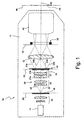
- FIG. 1 shows a meridional section of an illumination system according to the present invention that is to be used in a projection exposure step-and-scan apparatus.
- the illumination system which is denoted in its entirety by 10, comprises a light source that is, in the embodiment shown, realized as an .excimer laser 14.
- the excimer laser 14 emits projection light that has a wavelength in the deep ultraviolet (DUV) spectral range, for example 193 nm.
- the projection light emerging from the exit facet of the laser 14 forms a coherent light bundle having a small cross section and a low divergence.
- the geometrical optical flux of the light bundle as emitted by the laser 14 is small.
- the light bundle then enters a beam expansion unit 16 in which the light bundle is expanded. Since the light bundle is diverted at refractive interfaces, the cross section of the light bundle is increased without altering the geometrical optical flux of the bundle. This is due to the fact that the geometrical optical flux is an invariable quantity for light bundles that are refracted at interfaces between optical media having differing indices of refraction.
- the diffractive optical element 18 comprises one or more diffraction gratings that deflect each impinging ray such that a divergence is introduced. In FIG. 1 this is schematically represented for an axial ray that is split into two diverging rays 20, 22.
- the diffractive optical element 18 thus modifies the angular distribution of the projection light bundle and also enlarges its geometrical optical flux. Since diffractive optical elements of this kind that are suited for this purpose are known in the art as such, see for example US 6 285 443 , the diffractive optical element will not be described in further detail below.
- the diffractive optical element 18 can also be replaced by any other kind of optical raster element, for example a micro-lens array in which the micro-lenses are formed by Fresnel zone plates. Further examples for optical raster elements that are suitable for this purpose are given in the aforementioned US 6 285 443 .
- the diffractive optical element 18 is positioned in an object plane 24 of a first objective 26 that is only indicated by a zoom lens group 25 and a pair 27 of axicon elements 27a, 27b.
- Reference numeral 28 denotes an exit pupil plane of the first objective 26.
- a field defining component 30, which will be explained in more detail below and consists of two optical raster elements, is positioned in the pupil plane 28 of the first objective 26.
- the field defining component 30 again introduces a divergence for each point and thus enlarges the geometrical optical flux of the projection light bundle a second time.
- the divergence introduced by the field defining component 30 is schematically represented in FIG. 1 by divergent rays 20a, 20b and 22a, 22b for the impinging rays 20 and 22.
- the diverging rays 20a, 20b and 22a, 22b enter a second objective 32 that is represented in FIG. 1 by a single condensor lens 32.
- the second objective 32 is arranged within the illumination system 10 such that its entrance pupil plane coincides with the exit pupil plane 28 of the first objective 26.
- the image plane 34 of the second objective 32 is a field plane in which a reticle masking (REMA) unit 38 is positioned.
- REMA reticle masking
- the reticle masking unit 38 comprises a first subunit having two pairs of opposing adjustable blades that delimit the illuminated field in a direction parallel to a scan direction of the exposure apparatus into which the illumination system 10 is integrated.
- the reticle masking unit 38 may also comprise a second subunit that delimits the illuminated field in a direction perpendicular to the scan direction.
- the second subunit has two opposing rows of adjacent blades that are arranged parallel to the scan direction and can be selectively inserted into the projection light bundle produced by the light source 14.
- Such a second subunit may be used for further improving the irradiance uniformity.
- An example for such a second subunit is given in EP 1 020 769 A2
- the reticle masking unit 38 thus forms a stop that ensures sharp edges of the illuminated field in the scan direction.
- a third objective 42 having an object plane that coincides with the image plane 34 of the second objective is arranged along an optical axis 44 of the illumination system 10.
- an image plane 46 of the third objective 42 which is also referred to as REMA objective, the reticle 40 is positioned.
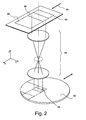
- FIG. 2 shows in a perspective schematic view how a pattern contained in the reticle 40 is imaged by a projection lens 50 onto a wafer 52 that is covered with a photoresist. While the reticle 40 is moved along the scan direction that is indicated by an arrow 54 and coincides with the X direction, an illuminated field 56 in the form of a rectangular slit scans a patterned area 58 of the reticle 40. At a given instance, only those parts of the patterned area 58 that are within the illuminated field 56 are projected by the projection lens 50 onto the wafer 52 and form an image 60 of the patterned area 58 on the wafer 52. The image 60 is reduced in size by the reduction factor of the projection lens 50 which may be equal to, for example, 1/4.
- FIGS. 3 and 4 show a field defining component 30 in a perspective view and a cross section, respectively.
- the field defining component 30 consists of a first refractive optical element 62 and a scattering plate 64.
- the refractive optical element 62 comprises a plurality of cylindrical micro-lenses 65, 66 that are oriented with their longitudinal axes along the X-direction. Each pair of adjacent micro-lenses 65, 66 have curvatures with opposite signs so that concave micro-lenses 65 and convex micro-lenses 66 alternate.
- FIGS. 3 and 4 only several cylindrical micro-lenses 65, 66 are shown. In reality, there may be many hundreds of such micro-lenses.
- the scattering plate 64 is a special diffractive optical element that is usually referred to as computer generated hologram (CGH). Such CHGs can be designed such that the geometrical optical flux is increased only in one direction or in both directions.
- CGH computer generated hologram
- the width of the line is mainly determined by the intensity distribution (laser profile) of the excimer laser 14.
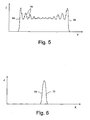
- FIG. 5 shows the intensity distribution that would be generated by the refractive optical element 62 in the reticle plane 46 in the Y-direction, i.e. perpendicular to the scan direction, if the scattering plate 64 was not present.
- this intensity distribution has steep slopes 68 and a number of ripples 70 whose altitude increases towards the slopes 68. If the reticle 40 was illuminated with a projection light bundle having the intensity distribution shown in FIG. 5 along the Y-direction, this would result in considerable undesired structure size variations of the microstructured device that is to be produced by the exposure projection apparatus.
- FIG. 6 shows the intensity distribution produced by the refractive optical element 62 in the reticle plane 46 in the X-direction, i.e. the scan direction.
- the intensity distribution is mainly given by the laser profile and thus has a Gaussian shape with two steep slopes 72.
- FIGS. 7 and 8 show graphs that illustrate the intensity distribution that would be generated by the scattering plate 64 in the reticle plane 46 in the Y- and X-direction, respectively, if the refractive optical element 62 was not present.
- the scattering plate 64 is designed such that it produces in the Y-direction, i.e. perpendicular to the scan direction, an intensity distribution with steep slopes 76 and a small flat section 78.
- a broader intensity distribution 77 is produced that has approximately a Gaussian shape.
- the combination of the refractive optical element 62 and the scattering plate 64 results in intensity distributions that can mathematically be described as convolutions of the intensity distributions produced by each element alone. If seen from a more illustrative point of view, the scattering plate 64 blurs the intensity distribution produced by the refractive optical element 62 in both directions to different degrees. This results in a considerable improvement of the uniformity of the intensity distribution on the photoresist. This is explained in the following with reference to FIGS. 9 and 10 .
- FIG. 9 shows the resulting intensity distribution caused by the field defining component 30 in the reticle plane 46 in the Y-direction, i.e. perpendicular to the scan direction.
- the convolution of the intensity distributions shown in FIGS. 5 and 7 results in an intensity distribution having an almost completely flat section 80 and slightly broader sloped parts 82 that delimit the intensity distributions at the lateral sides of the illuminated field 56.
- the flat section 80 is a result of the blurring effect that is caused by the scattering plate 64 and eliminates the ripples 70.
- This blurring effect is illustrated in FIG. 3 by two light rays 79a and 79b that enter the refractive optical element 62 in the direction indicated by arrows.
- the rays 79a, 79b undergo refraction at curved surfaces 81 of the cylindrical micro-lenses 65, 66 so that the geometrical optical flux is increased.
- the refracted rays 79a, 79b then enter the scattering plate 64 where the geometrical optical flux is increased a second time so that the rays 79a, 79b emerge from the scattering plate 64 not as single rays but as diverging bundles 83a and 83b, respectively.
- the angular distribution within the bundles 83a, 83b is determined by the pattern of the diffractive structures in the computer generated hologram (CHG) that forms the scattering plate 64.
- CHG computer generated hologram
- the blades of the first subunit of the reticle masking unit 38 are adjusted so that they stop out the slopes 82 completely.
- the position of the blades is indicated in FIG. 9 by broken lines 84. Since both slopes 82 are steep, the dotted areas 86 under these slopes 82 are small. These dotted areas 84 represent the light energy that is lost by stopping out this part of the illuminated field 56. The steeper the slopes 76 of the intensity distribution produced by the scattering plate 64 alone (see FIG. 7 ), the smaller are the dotted areas 84 and thus the light losses caused by the stops of the reticle masking unit 38 in the Y-direction.
- FIG. 10 shows the intensity distribution produced by the combination of the refractive optical element 62 and the scattering plate 64 in the reticle plane 46 in the X-direction, i.e. the scan direction.
- the convolution of the narrow line of Gaussian shape, which is produced by the refractive optical element 62 and shown in FIG. 6 , with the Gaussian intensity distribution that is produced by the scattering plate 62 and shown in FIG. 8 results in an intensity distribution that has also Gaussian slopes 86. This is due to the fact that the convolution of two Gaussian functions does not alter the form and thus yields again a Gaussian function.
- the broad Gaussian slopes 86 of the intensity distribution shown in FIG. 10 have the significant advantage that the pulse quantization effect cannot occur. This considerably improves the uniformity of the irradiance on the photoresist.
- FIG. 11 shows a graph illustrating the light intensity to which a first point on the patterned area 58 is exposed while moving along the scan direction X through the projection light bundle.
- the time window during which this point can be exposed to projection light has a length T.
- Light pulses that are emitted by the excimer laser 14 are represented by elongated rectangles P1, P2, ..., P9.
- P1, P2, ..., P9 Light pulses that are emitted by the excimer laser 14 are represented by elongated rectangles P1, P2, ..., P9.
- P4, P5, and P6 are consecutive pulses during its movement through the projection light bunde.
- FIG. 12 shows a similar graph, but for a second point on the patterned area 58 which is positioned - if seen in the scan direction X - in front of the first point so that it is exposed earlier.
- the time window of length T has now a different time relationship to the sequence of pulses P1 to P9.
- not only three pulses, but four pulses P4, P5, P6 and P7 contribute to the irradiance on the second point during the time interval of length T.
- the first point receives only three quarters of the light energy that is received by the second point.
- different points on the patterned area 58 are not uniformly irradiated although each light pulse P1 to P9 is assumed to have the same intensity.
- FIG. 13 shows the situation for the intensity distribution in the X direction which is produced by the combination of the refractive optical element 62 and the scattering plate 64. Due to the smooth slopes 86, the light pulses P1 to P9 do not contribute equally to the irradiance on a specific point on the patterned area 58 of the reticle 40. Instead, the light pulses P4, P5, P7 and P8 contribute with less energy to the irradiance on a specific point. It has been found out that the overall irradiance, i.e. the sum of the areas of the rectangles drawn in FIG. 13 in solid lines, is independent from the position of the time window with respect to the sequence of light pulses P1 to P9. In other words, shifting the light intensity distribution 88 along the time axis does not alter the total area of the rectangles drawn in solid lines.
- the intensity distribution produced by the scattering plate 64 alone can be identical for both the X-direction and the Y-direction. If this intensity distribution has a Gaussian shape as shown in FIG. 8 , this will result in larger light losses because the dotted areas 84 (see FIG. 9 ) then become larger.
- the manufacture of scattering plates that produce rotationally symmetrical intensity distributions is easier and cheaper from a technical point of view.
- the scattering plate 64 can then be realized as a refractive optical element having a plurality of micro-lenses whose shapes differ randomly. Such a scattering plate produces a rotationally symmetrical intensity distribution.
- the intensity distribution in the X-direction does not need to be (approximately) Gaussian.
- the scattering plate 64 may then produce a rectangular rotationally symmetric intensity distribution, because the blurring of the ripples 70 does not require a Gaussian distribution.
- the refractive optical element 62 comprises not only cylindrical microlenses 65 that are arranged along the Y-direction, but also cylindrical micro-lenses that are arranged along the X-direction. This will produce a rectangle instead of a narrow line in the reticle plane 46.
- two different refractive elements with cylindrical microlenses may be provided that differ with respect to the orientation of the micro-lenses. Since the geometrical optical flux is increased in both directions X, Y by the refractive optical element 62 alone, the scattering plate does not have to increase the geometrical optical flux significantly. Instead, it can be designed such that it merely blurs the ripples 70 in the intensity distribution that are typical for refractive optical elements. If desired it can also broaden the slope of the intensity distribution produced by the refractive optical element in the scan direction X in order to reduce the pulse quantization effect.
- the scattering plate 64 can, of course, also be positioned on the other side of the refractive optical element 62 so that the projection light is scattered before it enters the refractive optical element 62. It is also envisaged to use more than one scattering plates or to use a plate in which scattering structures are applied to both surfaces.
- a manipulator 91 (see FIG. 1 ) that is adapted to move the scattering plate 64 within the exit pupil 28.
- Such a movement could be a translational movement within this plane or a rotation around the optical axis 44. Adverse effects of possible non-uniformities within the scattering plate are thus eliminated.
- a cascade of many scattering plates 64 that rotate in different direction and with different velocities can be provided.
- FIGS. 14 and 15 show another field defining component 30' in a horizontal cross-section and a planar top view, respectively.
- the field defining component 30' comprises a refractive optical element 62' having a plurality of laterally adjacent cylinder lenses 65 that are arranged along the X-direction, i.e. parallel to the scan direction.
- the main difference to the field defining component shown in FIGS. 3 and 4 is that the field defining component 30' comprises instead of a scattering plate 64 a diffractive optical element 90 that is formed on a flat surface 92 of the refractive optical element 62'.
- the diffractive optical element 90 increases the geometrical optical flux both in the X-direction and also in the Y-direction. Since the refractive optical element 62' generates a broad intensity distribution similar to the one shown in FIG. 5 , the increase of the geometrical optical flux caused by the diffractive optical element 90 can be small in both directions. As a consequence, the diffractive optical element 90 can be realized as a blazed grating in which blaze flanks are approximated by a larger number of steps, for example eight. The better the approximation of the blaze flanks by a stepped curve, the higher is the diffraction efficiency of the grating. Apart from that, the larger diffraction structures have the advantage that they are considerably larger than the wavelength of the projection light. As a result, the diffractive optical element does not polarize the projection light bundle as is the case with diffractive elements that have diffraction structures whose size is comparable to the wavelength.
- the field defining component 30' has a similar function as the field defining component 30 shown in FIGS. 4 and 5 . Due to the increase of the geometrical optical flux in the Y-direction the ripples 70 that are present in the intensity distribution produced by the refractive optical element 62' can be eliminated to a large degree. In addition, the steep slopes 72 of the intensity distribution produced by the refractive optical element 62' in the X-direction can be broadened so that it approximates the ideal Gaussian shape as shown in FIG. 10 . Thus also the field defining component shown in FIGS. 14 and 15 improves the uniformity of the irradiance in the reticle plane by eliminating ripples in the Y-direction and reducing the pulse quantization effect.
- FIG. 16 shows another field defining component which is denoted in its entirety by 30" .
- the field defining component 30" differs from the field defining component 30' shown in FIGS. 14 and 15 in that the diffractive optical element is not provided at the flat surface 92 of the refractive optical element 62', but on its curved surface 81.
- the diffractive optical element 90" can be realized, for example, as a computer generated hologram.
- the field defining component 30" has substantially the same effect as the field defining component 30' shown in FIGS. 14 and 15 .
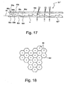
- FIG. 17 another field defining component is illustrated in a horizontal cross-section and denoted in its entirety by 30"'.
- the field defining component 30"' comprises a refractive optical element 62"' that is composed of a regular array of elongated prisms 92a, 92b, 92c, 92d whose longitudinal axis is aligned parallel to the Y-direction, i.e. perpendicular to the scan direction.
- the prisms 92a, 92b, 92c, 92d may have a length in the Y-direction of approximately 1 to 3 mm.
- Each prism 92a, 92b, 92c, 92d has a triangular cross-section with different angles ⁇ between a reference plane 94 and hypotenuse areas 96a, 96b, 96c and 96d.
- the prisms 92a, 92b, 92c, 92d produce in the reticle plane 46 a pattern of little bright spots 98 as is shown in FIG. 18 .
- the field defining component 30"' comprises a diffractive optical element 100 that increases the geometrical optical flux both in the X-direction and the Y-direction. This additionally blurs the bright spots 98 so that an almost uniform intensity distribution in the reticle plane 46 may be achieved. In FIG. 18 this is indicated by hexagonal areas 102 that represent the area over which the light energy is distributed from each bright spot 98 by the diffractive optical element 100.
- the increase of the geometrical optical flux caused by the diffractive optical element 100 is comparatively small so that this element can be manufactured with comparatively large diffraction structures.
- the diffractive optical element 100 can have a high diffraction efficiency and does not significantly affect the polarization state of the projection light.
- the diffractive optical element 100 may be subdivided into a plurality of different zones that are separated in FIG. 17 by dotted lines and exemplarily indicated by 99a, 99b.
- the configuration of the diffractive structures contained in each zone is adapted to the angles that the light rays emerging from the prisms 92a, 92b, 92c, 92d form with the reference plane 94.
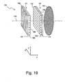
- FIGS. 19 , 20 and 21 show an embodiment of a field defining component in a perspective view and in sections parallel to the Y-Z plane and the X-Z plane, respectively. These illustrations are not to scale and considerably simplified.
- the field defining component which is denoted in its entirety by 130, comprises two groups G1, G2 of arrays of cylindrical micro-lenses.
- Group G1 includes a first array 162 of parallel first cylindrical micro-lenses 164 each having a longitudinal axis aligned along the Y direction and a back focal length f 1 .
- Group G1 further includes a second array 166 of parallel second cylindrical micro-lenses 168 each having a longitudinal axis aligned along the X direction and a back focal length f 2 ⁇ f 1 .
- Plane back surfaces of the second cylindrical micro-lenses 168 are immediately attached to plane back surfaces of the first cylindrical micro-lenses 164.
- the third array 170 is positioned along an optical axis 144 such that curved front surfaces of the third cylindrical micro-lenses 172 face the curved back surfaces of the second cylindrical micro-lenses 168.
- focal lines of the second cylindrical microlenses 168 are at least approximately on the curved surfaces of the third cylindrical micro-lenses 172, very high light intensities, which may destroy the material of the micro-micro-lenses or a substrate supporting the latter, cannot occur.
- the field defining component 130 further comprises a scattering plate 180 which is arranged in the immediate vicinity of one of the arrays, here behind the fourth array 174.
- the scattering plate 180 may be positioned in front of the first array 162 or between the groups G1, G2.
- the scattering plate 180 further enhances the irradiance uniformity in the reticle plane 46.
Landscapes
- Physics & Mathematics (AREA)
- General Physics & Mathematics (AREA)
- Exposure Of Semiconductors, Excluding Electron Or Ion Beam Exposure (AREA)
- Exposure And Positioning Against Photoresist Photosensitive Materials (AREA)
Applications Claiming Priority (2)
| Application Number | Priority Date | Filing Date | Title |
|---|---|---|---|
| US54510504P | 2004-02-17 | 2004-02-17 | |
| PCT/EP2005/001501 WO2005078522A2 (en) | 2004-02-17 | 2005-02-15 | Illumination system for a microlithographic projection exposure apparatus |
Publications (2)
| Publication Number | Publication Date |
|---|---|
| EP1716458A2 EP1716458A2 (en) | 2006-11-02 |
| EP1716458B1 true EP1716458B1 (en) | 2011-06-01 |
Family
ID=34860514
Family Applications (1)
| Application Number | Title | Priority Date | Filing Date |
|---|---|---|---|
| EP05707395A Expired - Lifetime EP1716458B1 (en) | 2004-02-17 | 2005-02-15 | Illumination system for a microlithographic projection exposure apparatus |
Country Status (6)
| Country | Link |
|---|---|
| US (2) | US8004656B2 (enExample) |
| EP (1) | EP1716458B1 (enExample) |
| JP (1) | JP4846600B2 (enExample) |
| KR (1) | KR101170182B1 (enExample) |
| AT (1) | ATE511668T1 (enExample) |
| WO (1) | WO2005078522A2 (enExample) |
Families Citing this family (26)
| Publication number | Priority date | Publication date | Assignee | Title |
|---|---|---|---|---|
| JP4846600B2 (ja) | 2004-02-17 | 2011-12-28 | カール・ツァイス・エスエムティー・ゲーエムベーハー | マイクロリソグラフィ投射露光装置用照射システム |
| TWI545352B (zh) * | 2006-02-17 | 2016-08-11 | 卡爾蔡司Smt有限公司 | 用於微影投射曝光設備之照明系統 |
| WO2007093433A1 (de) | 2006-02-17 | 2007-08-23 | Carl Zeiss Smt Ag | Beleuchtungssystem für die mikro-lithographie, projektionsbelichtungsanlage mit einem derartigen beleuchtungssystem |
| KR101306503B1 (ko) | 2006-02-17 | 2013-09-09 | 칼 짜이스 에스엠티 게엠베하 | 마이크로리소그래피 투영 노광 장치의 조명 시스템용 광 인터그레이터 |
| DE102007023411A1 (de) * | 2006-12-28 | 2008-07-03 | Carl Zeiss Smt Ag | Optisches Element, Beleuchtungsoptik für die Mikrolithographie mit mindestens einem derartigen optischen Element sowie Beleuchtungssystem mit einer derartigen Beleuchtungsoptik |
| WO2008086827A1 (en) | 2007-01-16 | 2008-07-24 | Carl Zeiss Smt Ag | Projection exposure method and projection exposure system therefor |
| JP2008182244A (ja) * | 2007-01-25 | 2008-08-07 | Carl Zeiss Smt Ag | マイクロリソグラフ投影露光装置の照明系用光インテグレータ |
| DE102008006637A1 (de) | 2007-01-25 | 2008-07-31 | Carl Zeiss Smt Ag | Optischer Integrator für ein Beleuchtungssystem einer mikrolithographischen Projektionsbelichtungsanlage |
| WO2008094141A1 (en) | 2007-01-29 | 2008-08-07 | Celloptic, Inc. | System, apparatus and method for extracting image cross-sections of an object from received electromagnetic radiation |
| JP5345132B2 (ja) * | 2007-04-25 | 2013-11-20 | カール・ツァイス・エスエムティー・ゲーエムベーハー | マイクロリソグラフィ露光装置においてマスクを照明するための照明系 |
| EP2146248B1 (en) | 2008-07-16 | 2012-08-29 | Carl Zeiss SMT GmbH | Illumination system of a microlithographic projection exposure apparatus |
| DE102008036569A1 (de) * | 2008-07-31 | 2009-10-22 | Carl Zeiss Laser Optics Gmbh | Wabenkondensor und Vorrichtung zum Aufschmelzen von Schichten auf ein Substrat |
| EP2169464A1 (en) | 2008-09-29 | 2010-03-31 | Carl Zeiss SMT AG | Illumination system of a microlithographic projection exposure apparatus |
| EP2317386B1 (en) | 2008-12-23 | 2012-07-11 | Carl Zeiss SMT GmbH | Illumination system of a microlithographic projection exposure apparatus |
| JP5587917B2 (ja) | 2009-03-13 | 2014-09-10 | カール・ツァイス・エスエムティー・ゲーエムベーハー | マイクロリソグラフィ投影露光装置 |
| KR101646814B1 (ko) | 2009-03-19 | 2016-08-08 | 칼 짜이스 에스엠티 게엠베하 | 마이크로리소그래피 투영 노광 장치의 조명 시스템 |
| US8164046B2 (en) | 2009-07-16 | 2012-04-24 | Carl Zeiss Smt Gmbh | Illumination system for illuminating a mask in a microlithographic projection exposure apparatus |
| KR101373380B1 (ko) | 2009-07-17 | 2014-03-13 | 칼 짜이스 에스엠티 게엠베하 | 마이크로리소그래피 투영 노광 장치 및 그에 포함된 광학 표면에 관한 파라미터의 측정 방법 |
| EP2354853B1 (en) | 2010-02-09 | 2013-01-02 | Carl Zeiss SMT GmbH | Optical raster element, optical integrator and illumination system of a microlithographic projection exposure apparatus |
| DE102013204443A1 (de) * | 2013-03-14 | 2014-10-02 | Carl Zeiss Smt Gmbh | Optische Baugruppe zur Lichtleitwerterhöhung |
| US8875066B2 (en) * | 2013-03-15 | 2014-10-28 | Synopsys, Inc. | Performing image calculation based on spatial coherence |
| CN103412465B (zh) | 2013-07-01 | 2015-04-15 | 中国科学院上海光学精密机械研究所 | 步进扫描投影光刻机的照明系统 |
| WO2017108448A1 (en) * | 2015-12-22 | 2017-06-29 | Carl Zeiss Smt Gmbh | Illumination system of a microlithographic apparatus |
| CN105589300A (zh) * | 2016-01-07 | 2016-05-18 | 中国科学院上海光学精密机械研究所 | 一种光刻照明系统 |
| US10823531B2 (en) * | 2017-02-09 | 2020-11-03 | Lightforce Usa, Inc. | Reticle disc with fiber illuminated aiming dot |
| CN114127617A (zh) * | 2019-07-23 | 2022-03-01 | 埃博茨股份有限公司 | 用于具有高精度和实时对象跟踪的3d姿态测量的系统和方法 |
Citations (1)
| Publication number | Priority date | Publication date | Assignee | Title |
|---|---|---|---|---|
| US6307682B1 (en) * | 2000-02-16 | 2001-10-23 | Silicon Valley Group, Inc. | Zoom illumination system for use in photolithography |
Family Cites Families (56)
| Publication number | Priority date | Publication date | Assignee | Title |
|---|---|---|---|---|
| DE2125889A1 (de) * | 1971-05-25 | 1972-11-30 | Siemens Ag | Kohärent-optischer Vielkanal-Korrelator |
| FR2406236A1 (fr) * | 1976-12-10 | 1979-05-11 | Thomson Csf | Dispositif optique a source coherente pour le transfert rapide de motifs sur substrats, applique a la realisation de composants et circuits a microstructures |
| JPS58147708A (ja) * | 1982-02-26 | 1983-09-02 | Nippon Kogaku Kk <Nikon> | 照明用光学装置 |
| JPS60232552A (ja) * | 1984-05-02 | 1985-11-19 | Canon Inc | 照明光学系 |
| JPS62115718A (ja) * | 1985-11-14 | 1987-05-27 | Canon Inc | 照明光学系 |
| US4733944A (en) * | 1986-01-24 | 1988-03-29 | Xmr, Inc. | Optical beam integration system |
| JPS6461716A (en) * | 1987-08-31 | 1989-03-08 | Canon Kk | Illuminator |
| JP3148818B2 (ja) * | 1990-11-15 | 2001-03-26 | 株式会社ニコン | 投影型露光装置 |
| JP3303322B2 (ja) * | 1992-01-31 | 2002-07-22 | 株式会社ニコン | 投影露光装置及び方法、並びに素子製造方法 |
| US6710855B2 (en) * | 1990-11-15 | 2004-03-23 | Nikon Corporation | Projection exposure apparatus and method |
| US6967710B2 (en) * | 1990-11-15 | 2005-11-22 | Nikon Corporation | Projection exposure apparatus and method |
| JPH07128590A (ja) * | 1993-10-29 | 1995-05-19 | Olympus Optical Co Ltd | 縮小投影レンズ |
| US6285443B1 (en) | 1993-12-13 | 2001-09-04 | Carl-Zeiss-Stiftung | Illuminating arrangement for a projection microlithographic apparatus |
| DE19520563A1 (de) * | 1995-06-06 | 1996-12-12 | Zeiss Carl Fa | Beleuchtungseinrichtung für ein Projektions-Mikrolithographie-Gerät |
| JP3278277B2 (ja) * | 1994-01-26 | 2002-04-30 | キヤノン株式会社 | 投影露光装置及びこれを用いたデバイス製造方法 |
| US5850300A (en) * | 1994-02-28 | 1998-12-15 | Digital Optics Corporation | Diffractive beam homogenizer having free-form fringes |
| JPH07306304A (ja) * | 1994-05-11 | 1995-11-21 | Ricoh Opt Ind Co Ltd | オプチカル・ホモジナイザー |
| US5963305A (en) * | 1996-09-12 | 1999-10-05 | Canon Kabushiki Kaisha | Illumination system and exposure apparatus |
| US6829091B2 (en) * | 1997-02-07 | 2004-12-07 | Canon Kabushiki Kaisha | Optical system and optical instrument with diffractive optical element |
| US6013401A (en) | 1997-03-31 | 2000-01-11 | Svg Lithography Systems, Inc. | Method of controlling illumination field to reduce line width variation |
| JP3264224B2 (ja) * | 1997-08-04 | 2002-03-11 | キヤノン株式会社 | 照明装置及びそれを用いた投影露光装置 |
| US5844727A (en) * | 1997-09-02 | 1998-12-01 | Cymer, Inc. | Illumination design for scanning microlithography systems |
| JPH1197340A (ja) * | 1997-09-17 | 1999-04-09 | Omron Corp | 露光光学系、光加工装置、露光装置及び光結合装置 |
| JP4329266B2 (ja) * | 1998-03-24 | 2009-09-09 | 株式会社ニコン | 照明装置、露光方法及び装置、並びにデバイス製造方法 |
| US6404499B1 (en) * | 1998-04-21 | 2002-06-11 | Asml Netherlands B.V. | Lithography apparatus with filters for optimizing uniformity of an image |
| EP0952491A3 (en) | 1998-04-21 | 2001-05-09 | Asm Lithography B.V. | Lithography apparatus |
| DE10053587A1 (de) * | 2000-10-27 | 2002-05-02 | Zeiss Carl | Beleuchtungssystem mit variabler Einstellung der Ausleuchtung |
| DE19855106A1 (de) | 1998-11-30 | 2000-05-31 | Zeiss Carl Fa | Beleuchtungssystem für die VUV-Mikrolithographie |
| DE10040898A1 (de) * | 2000-08-18 | 2002-02-28 | Zeiss Carl | Beleuchtungssystem für die Mikrolithographie |
| US6583937B1 (en) | 1998-11-30 | 2003-06-24 | Carl-Zeiss Stiftung | Illuminating system of a microlithographic projection exposure arrangement |
| US6563567B1 (en) * | 1998-12-17 | 2003-05-13 | Nikon Corporation | Method and apparatus for illuminating a surface using a projection imaging apparatus |
| JP2000277421A (ja) * | 1999-03-26 | 2000-10-06 | Nikon Corp | 照明装置 |
| US6469830B1 (en) * | 1999-04-01 | 2002-10-22 | Honeywell Inc. | Display screen and method of manufacture therefor |
| JP2001174615A (ja) * | 1999-04-15 | 2001-06-29 | Nikon Corp | 回折光学素子、該素子の製造方法、該素子を備える照明装置、投影露光装置、露光方法、及び光ホモジナイザー、該光ホモジナイザーの製造方法 |
| JP2001066442A (ja) * | 1999-06-22 | 2001-03-16 | Mitsubishi Electric Corp | グレーティング加工装置 |
| JP2001042253A (ja) * | 1999-08-04 | 2001-02-16 | Minolta Co Ltd | レーザー照射光学系 |
| US6497488B1 (en) * | 1999-08-06 | 2002-12-24 | Ricoh Company, Ltd. | Illumination system and projector |
| JP2002118043A (ja) * | 2000-10-05 | 2002-04-19 | Nikon Corp | 照明光学装置および該照明光学装置を備えた露光装置 |
| JP2002222761A (ja) * | 2000-11-22 | 2002-08-09 | Nikon Corp | 照明光学装置および該照明光学装置を備えた露光装置 |
| JP2002217083A (ja) * | 2001-01-12 | 2002-08-02 | Canon Inc | 照明装置及び露光装置 |
| JP3634782B2 (ja) * | 2001-09-14 | 2005-03-30 | キヤノン株式会社 | 照明装置、それを用いた露光装置及びデバイス製造方法 |
| JP4859311B2 (ja) * | 2001-09-17 | 2012-01-25 | 株式会社リコー | レーザ照明光学系、該光学系を用いた露光装置、レーザ加工機、及び投射装置 |
| JP3987350B2 (ja) * | 2001-11-16 | 2007-10-10 | 株式会社リコー | レーザ照明光学系及びそれを用いた露光装置、レーザ加工装置、投射装置 |
| JP2003173956A (ja) * | 2001-12-05 | 2003-06-20 | Canon Inc | 露光方法及び装置 |
| AU2003222799A1 (en) | 2002-04-15 | 2003-10-27 | Carl Zeiss Smt Ag | Interferometric measuring device and projection illumination installation comprising one such measuring device |
| JP4250906B2 (ja) | 2002-04-23 | 2009-04-08 | コニカミノルタホールディングス株式会社 | 光学素子 |
| JP4324957B2 (ja) * | 2002-05-27 | 2009-09-02 | 株式会社ニコン | 照明光学装置、露光装置および露光方法 |
| JP4207478B2 (ja) * | 2002-07-12 | 2009-01-14 | 株式会社ニコン | オプティカルインテグレータ、照明光学装置、露光装置および露光方法 |
| TW589904B (en) * | 2002-12-18 | 2004-06-01 | Prodisc Technology Inc | Rear projection screen, optical component of rear projection screen and method for manufacturing thereof |
| WO2005015310A2 (en) | 2003-07-16 | 2005-02-17 | Carl Zeiss Smt Ag | Illumination system for a microlithographic projection exposure apparatus |
| JP4846600B2 (ja) | 2004-02-17 | 2011-12-28 | カール・ツァイス・エスエムティー・ゲーエムベーハー | マイクロリソグラフィ投射露光装置用照射システム |
| JP2005310942A (ja) * | 2004-04-20 | 2005-11-04 | Canon Inc | 露光装置、露光方法、及びそれを用いたデバイス製造方法 |
| US7079225B2 (en) * | 2004-09-14 | 2006-07-18 | Asml Netherlands B.V | Lithographic apparatus and device manufacturing method |
| KR101306503B1 (ko) * | 2006-02-17 | 2013-09-09 | 칼 짜이스 에스엠티 게엠베하 | 마이크로리소그래피 투영 노광 장치의 조명 시스템용 광 인터그레이터 |
| US20070253058A1 (en) * | 2006-05-01 | 2007-11-01 | Bright View Technologies, Inc. | Brightness enhancement structures including optical microstructures to provide elliptical diffusion patterns and methods of fabricating and operating the same |
| JP4261591B2 (ja) * | 2007-03-30 | 2009-04-30 | アドバンスド・マスク・インスペクション・テクノロジー株式会社 | 照明光学装置および試料検査装置 |
-
2005
- 2005-02-15 JP JP2006552571A patent/JP4846600B2/ja not_active Expired - Fee Related
- 2005-02-15 AT AT05707395T patent/ATE511668T1/de not_active IP Right Cessation
- 2005-02-15 KR KR1020067016279A patent/KR101170182B1/ko not_active Expired - Lifetime
- 2005-02-15 WO PCT/EP2005/001501 patent/WO2005078522A2/en not_active Ceased
- 2005-02-15 EP EP05707395A patent/EP1716458B1/en not_active Expired - Lifetime
-
2006
- 2006-08-17 US US11/505,408 patent/US8004656B2/en not_active Expired - Fee Related
-
2011
- 2011-07-12 US US13/181,033 patent/US8730455B2/en not_active Expired - Fee Related
Patent Citations (1)
| Publication number | Priority date | Publication date | Assignee | Title |
|---|---|---|---|---|
| US6307682B1 (en) * | 2000-02-16 | 2001-10-23 | Silicon Valley Group, Inc. | Zoom illumination system for use in photolithography |
Also Published As
| Publication number | Publication date |
|---|---|
| ATE511668T1 (de) | 2011-06-15 |
| JP4846600B2 (ja) | 2011-12-28 |
| US8730455B2 (en) | 2014-05-20 |
| KR20060123538A (ko) | 2006-12-01 |
| JP2007525027A (ja) | 2007-08-30 |
| US8004656B2 (en) | 2011-08-23 |
| WO2005078522A3 (en) | 2006-03-02 |
| EP1716458A2 (en) | 2006-11-02 |
| US20110285978A1 (en) | 2011-11-24 |
| KR101170182B1 (ko) | 2012-08-01 |
| WO2005078522A2 (en) | 2005-08-25 |
| US20070206171A1 (en) | 2007-09-06 |
Similar Documents
| Publication | Publication Date | Title |
|---|---|---|
| EP1716458B1 (en) | Illumination system for a microlithographic projection exposure apparatus | |
| CN101384966B (zh) | 用于微光刻投影曝光设备的照射系统 | |
| US6583937B1 (en) | Illuminating system of a microlithographic projection exposure arrangement | |
| KR101751581B1 (ko) | 마이크로리소그래픽 투영 노광 장치의 조명 시스템 | |
| KR101470769B1 (ko) | 마이크로리소그래픽 투영 노광 장치의 조명 시스템 | |
| US9804499B2 (en) | Illumination system of a microlithographic projection exposure apparatus | |
| EP2020679A1 (en) | Illuminating optical apparatus, exposure apparatus, and device manufacturing method | |
| US20180164691A1 (en) | Projection exposure methods and systems | |
| US8724080B2 (en) | Optical raster element, optical integrator and illumination system of a microlithographic projection exposure apparatus | |
| US20070024836A1 (en) | Illumination system for a microlithographic projection exposure apparatus | |
| JP2008182244A (ja) | マイクロリソグラフ投影露光装置の照明系用光インテグレータ | |
| US20070216887A1 (en) | Illumination System for a Microlithographic Projection Exposure Apparatus | |
| US20090009744A1 (en) | Illumination system for a microlithographic projection exposure apparatus | |
| Michaloski | Requirements and designs of illuminators for microlithography | |
| WO2017108448A1 (en) | Illumination system of a microlithographic apparatus |
Legal Events
| Date | Code | Title | Description |
|---|---|---|---|
| PUAI | Public reference made under article 153(3) epc to a published international application that has entered the european phase |
Free format text: ORIGINAL CODE: 0009012 |
|
| 17P | Request for examination filed |
Effective date: 20060630 |
|
| AK | Designated contracting states |
Kind code of ref document: A2 Designated state(s): AT BE BG CH CY CZ DE DK EE ES FI FR GB GR HU IE IS IT LI LT LU MC NL PL PT RO SE SI SK TR |
|
| 17Q | First examination report despatched |
Effective date: 20070209 |
|
| DAX | Request for extension of the european patent (deleted) | ||
| RAP1 | Party data changed (applicant data changed or rights of an application transferred) |
Owner name: CARL ZEISS SMT AG |
|
| GRAP | Despatch of communication of intention to grant a patent |
Free format text: ORIGINAL CODE: EPIDOSNIGR1 |
|
| RAP1 | Party data changed (applicant data changed or rights of an application transferred) |
Owner name: CARL ZEISS SMT GMBH |
|
| GRAS | Grant fee paid |
Free format text: ORIGINAL CODE: EPIDOSNIGR3 |
|
| GRAA | (expected) grant |
Free format text: ORIGINAL CODE: 0009210 |
|
| AK | Designated contracting states |
Kind code of ref document: B1 Designated state(s): AT BE BG CH CY CZ DE DK EE ES FI FR GB GR HU IE IS IT LI LT LU MC NL PL PT RO SE SI SK TR |
|
| REG | Reference to a national code |
Ref country code: GB Ref legal event code: FG4D |
|
| REG | Reference to a national code |
Ref country code: CH Ref legal event code: EP |
|
| REG | Reference to a national code |
Ref country code: IE Ref legal event code: FG4D |
|
| REG | Reference to a national code |
Ref country code: DE Ref legal event code: R096 Ref document number: 602005028321 Country of ref document: DE Effective date: 20110714 |
|
| REG | Reference to a national code |
Ref country code: NL Ref legal event code: T3 |
|
| PG25 | Lapsed in a contracting state [announced via postgrant information from national office to epo] |
Ref country code: LT Free format text: LAPSE BECAUSE OF FAILURE TO SUBMIT A TRANSLATION OF THE DESCRIPTION OR TO PAY THE FEE WITHIN THE PRESCRIBED TIME-LIMIT Effective date: 20110601 Ref country code: SE Free format text: LAPSE BECAUSE OF FAILURE TO SUBMIT A TRANSLATION OF THE DESCRIPTION OR TO PAY THE FEE WITHIN THE PRESCRIBED TIME-LIMIT Effective date: 20110601 |
|
| PG25 | Lapsed in a contracting state [announced via postgrant information from national office to epo] |
Ref country code: ES Free format text: LAPSE BECAUSE OF FAILURE TO SUBMIT A TRANSLATION OF THE DESCRIPTION OR TO PAY THE FEE WITHIN THE PRESCRIBED TIME-LIMIT Effective date: 20110912 Ref country code: CY Free format text: LAPSE BECAUSE OF FAILURE TO SUBMIT A TRANSLATION OF THE DESCRIPTION OR TO PAY THE FEE WITHIN THE PRESCRIBED TIME-LIMIT Effective date: 20110601 Ref country code: GR Free format text: LAPSE BECAUSE OF FAILURE TO SUBMIT A TRANSLATION OF THE DESCRIPTION OR TO PAY THE FEE WITHIN THE PRESCRIBED TIME-LIMIT Effective date: 20110902 Ref country code: FI Free format text: LAPSE BECAUSE OF FAILURE TO SUBMIT A TRANSLATION OF THE DESCRIPTION OR TO PAY THE FEE WITHIN THE PRESCRIBED TIME-LIMIT Effective date: 20110601 Ref country code: AT Free format text: LAPSE BECAUSE OF FAILURE TO SUBMIT A TRANSLATION OF THE DESCRIPTION OR TO PAY THE FEE WITHIN THE PRESCRIBED TIME-LIMIT Effective date: 20110601 Ref country code: SI Free format text: LAPSE BECAUSE OF FAILURE TO SUBMIT A TRANSLATION OF THE DESCRIPTION OR TO PAY THE FEE WITHIN THE PRESCRIBED TIME-LIMIT Effective date: 20110601 |
|
| PG25 | Lapsed in a contracting state [announced via postgrant information from national office to epo] |
Ref country code: BE Free format text: LAPSE BECAUSE OF FAILURE TO SUBMIT A TRANSLATION OF THE DESCRIPTION OR TO PAY THE FEE WITHIN THE PRESCRIBED TIME-LIMIT Effective date: 20110601 |
|
| PG25 | Lapsed in a contracting state [announced via postgrant information from national office to epo] |
Ref country code: EE Free format text: LAPSE BECAUSE OF FAILURE TO SUBMIT A TRANSLATION OF THE DESCRIPTION OR TO PAY THE FEE WITHIN THE PRESCRIBED TIME-LIMIT Effective date: 20110601 Ref country code: IS Free format text: LAPSE BECAUSE OF FAILURE TO SUBMIT A TRANSLATION OF THE DESCRIPTION OR TO PAY THE FEE WITHIN THE PRESCRIBED TIME-LIMIT Effective date: 20111001 Ref country code: PT Free format text: LAPSE BECAUSE OF FAILURE TO SUBMIT A TRANSLATION OF THE DESCRIPTION OR TO PAY THE FEE WITHIN THE PRESCRIBED TIME-LIMIT Effective date: 20111003 Ref country code: CZ Free format text: LAPSE BECAUSE OF FAILURE TO SUBMIT A TRANSLATION OF THE DESCRIPTION OR TO PAY THE FEE WITHIN THE PRESCRIBED TIME-LIMIT Effective date: 20110601 |
|
| PG25 | Lapsed in a contracting state [announced via postgrant information from national office to epo] |
Ref country code: SK Free format text: LAPSE BECAUSE OF FAILURE TO SUBMIT A TRANSLATION OF THE DESCRIPTION OR TO PAY THE FEE WITHIN THE PRESCRIBED TIME-LIMIT Effective date: 20110601 Ref country code: RO Free format text: LAPSE BECAUSE OF FAILURE TO SUBMIT A TRANSLATION OF THE DESCRIPTION OR TO PAY THE FEE WITHIN THE PRESCRIBED TIME-LIMIT Effective date: 20110601 Ref country code: PL Free format text: LAPSE BECAUSE OF FAILURE TO SUBMIT A TRANSLATION OF THE DESCRIPTION OR TO PAY THE FEE WITHIN THE PRESCRIBED TIME-LIMIT Effective date: 20110601 |
|
| PLBE | No opposition filed within time limit |
Free format text: ORIGINAL CODE: 0009261 |
|
| STAA | Information on the status of an ep patent application or granted ep patent |
Free format text: STATUS: NO OPPOSITION FILED WITHIN TIME LIMIT |
|
| 26N | No opposition filed |
Effective date: 20120302 |
|
| PG25 | Lapsed in a contracting state [announced via postgrant information from national office to epo] |
Ref country code: IT Free format text: LAPSE BECAUSE OF FAILURE TO SUBMIT A TRANSLATION OF THE DESCRIPTION OR TO PAY THE FEE WITHIN THE PRESCRIBED TIME-LIMIT Effective date: 20110601 |
|
| REG | Reference to a national code |
Ref country code: DE Ref legal event code: R097 Ref document number: 602005028321 Country of ref document: DE Effective date: 20120302 |
|
| PG25 | Lapsed in a contracting state [announced via postgrant information from national office to epo] |
Ref country code: DK Free format text: LAPSE BECAUSE OF FAILURE TO SUBMIT A TRANSLATION OF THE DESCRIPTION OR TO PAY THE FEE WITHIN THE PRESCRIBED TIME-LIMIT Effective date: 20110601 |
|
| PG25 | Lapsed in a contracting state [announced via postgrant information from national office to epo] |
Ref country code: MC Free format text: LAPSE BECAUSE OF NON-PAYMENT OF DUE FEES Effective date: 20120229 |
|
| REG | Reference to a national code |
Ref country code: CH Ref legal event code: PL |
|
| GBPC | Gb: european patent ceased through non-payment of renewal fee |
Effective date: 20120215 |
|
| PG25 | Lapsed in a contracting state [announced via postgrant information from national office to epo] |
Ref country code: LI Free format text: LAPSE BECAUSE OF NON-PAYMENT OF DUE FEES Effective date: 20120229 Ref country code: CH Free format text: LAPSE BECAUSE OF NON-PAYMENT OF DUE FEES Effective date: 20120229 |
|
| REG | Reference to a national code |
Ref country code: IE Ref legal event code: MM4A |
|
| REG | Reference to a national code |
Ref country code: FR Ref legal event code: ST Effective date: 20121031 |
|
| PG25 | Lapsed in a contracting state [announced via postgrant information from national office to epo] |
Ref country code: IE Free format text: LAPSE BECAUSE OF NON-PAYMENT OF DUE FEES Effective date: 20120215 Ref country code: GB Free format text: LAPSE BECAUSE OF NON-PAYMENT OF DUE FEES Effective date: 20120215 Ref country code: FR Free format text: LAPSE BECAUSE OF NON-PAYMENT OF DUE FEES Effective date: 20120229 |
|
| PG25 | Lapsed in a contracting state [announced via postgrant information from national office to epo] |
Ref country code: BG Free format text: LAPSE BECAUSE OF FAILURE TO SUBMIT A TRANSLATION OF THE DESCRIPTION OR TO PAY THE FEE WITHIN THE PRESCRIBED TIME-LIMIT Effective date: 20110901 |
|
| PG25 | Lapsed in a contracting state [announced via postgrant information from national office to epo] |
Ref country code: TR Free format text: LAPSE BECAUSE OF FAILURE TO SUBMIT A TRANSLATION OF THE DESCRIPTION OR TO PAY THE FEE WITHIN THE PRESCRIBED TIME-LIMIT Effective date: 20110601 |
|
| PG25 | Lapsed in a contracting state [announced via postgrant information from national office to epo] |
Ref country code: LU Free format text: LAPSE BECAUSE OF NON-PAYMENT OF DUE FEES Effective date: 20120215 |
|
| PG25 | Lapsed in a contracting state [announced via postgrant information from national office to epo] |
Ref country code: HU Free format text: LAPSE BECAUSE OF FAILURE TO SUBMIT A TRANSLATION OF THE DESCRIPTION OR TO PAY THE FEE WITHIN THE PRESCRIBED TIME-LIMIT Effective date: 20050215 |
|
| PGFP | Annual fee paid to national office [announced via postgrant information from national office to epo] |
Ref country code: DE Payment date: 20170217 Year of fee payment: 13 |
|
| PGFP | Annual fee paid to national office [announced via postgrant information from national office to epo] |
Ref country code: NL Payment date: 20170216 Year of fee payment: 13 |
|
| REG | Reference to a national code |
Ref country code: DE Ref legal event code: R119 Ref document number: 602005028321 Country of ref document: DE |
|
| REG | Reference to a national code |
Ref country code: NL Ref legal event code: MM Effective date: 20180301 |
|
| PG25 | Lapsed in a contracting state [announced via postgrant information from national office to epo] |
Ref country code: NL Free format text: LAPSE BECAUSE OF NON-PAYMENT OF DUE FEES Effective date: 20180301 |
|
| PG25 | Lapsed in a contracting state [announced via postgrant information from national office to epo] |
Ref country code: DE Free format text: LAPSE BECAUSE OF NON-PAYMENT OF DUE FEES Effective date: 20180901 |
|
| P01 | Opt-out of the competence of the unified patent court (upc) registered |
Effective date: 20230525 |