EP1710806B1 - Mobile communication device having integrated embedded flash and sram memory - Google Patents
Mobile communication device having integrated embedded flash and sram memory Download PDFInfo
- Publication number
- EP1710806B1 EP1710806B1 EP06015160.2A EP06015160A EP1710806B1 EP 1710806 B1 EP1710806 B1 EP 1710806B1 EP 06015160 A EP06015160 A EP 06015160A EP 1710806 B1 EP1710806 B1 EP 1710806B1
- Authority
- EP
- European Patent Office
- Prior art keywords
- flash
- flash memory
- memory
- macros
- macro
- Prior art date
- Legal status (The legal status is an assumption and is not a legal conclusion. Google has not performed a legal analysis and makes no representation as to the accuracy of the status listed.)
- Expired - Lifetime
Links
Images


Classifications
-
- G—PHYSICS
- G11—INFORMATION STORAGE
- G11C—STATIC STORES
- G11C16/00—Erasable programmable read-only memories
- G11C16/02—Erasable programmable read-only memories electrically programmable
- G11C16/06—Auxiliary circuits, e.g. for writing into memory
-
- G—PHYSICS
- G11—INFORMATION STORAGE
- G11C—STATIC STORES
- G11C16/00—Erasable programmable read-only memories
- G11C16/02—Erasable programmable read-only memories electrically programmable
- G11C16/06—Auxiliary circuits, e.g. for writing into memory
- G11C16/26—Sensing or reading circuits; Data output circuits
-
- G—PHYSICS
- G11—INFORMATION STORAGE
- G11C—STATIC STORES
- G11C16/00—Erasable programmable read-only memories
- G11C16/02—Erasable programmable read-only memories electrically programmable
- G11C16/06—Auxiliary circuits, e.g. for writing into memory
- G11C16/22—Safety or protection circuits preventing unauthorised or accidental access to memory cells
-
- G—PHYSICS
- G11—INFORMATION STORAGE
- G11C—STATIC STORES
- G11C2216/00—Indexing scheme relating to G11C16/00 and subgroups, for features not directly covered by these groups
- G11C2216/12—Reading and writing aspects of erasable programmable read-only memories
- G11C2216/22—Nonvolatile memory in which reading can be carried out from one memory bank or array whilst a word or sector in another bank or array is being erased or programmed simultaneously
Definitions
- the invention generally relates to mobile communication devices such as cellular telephones and in particular to flash memory and static random access memory (SRAM) for use therein.
- SRAM static random access memory
- a flash memory is a type of non-volatile memory that retains stored information even after power is disconnected. This is in contrast with volatile memory devices, such as SRAM or dynamic RAM (DRAM), which lose data stored therein once power has been disconnected.
- flash memory is electrically erasable and reprogrammable within the system in which it is incorporated. This is in contrast with other non-volatile memory devices, such as erasable, programmable read-only memory (EPROM)which typically requires special voltages for reprogramming and, hence, is typically only reprogrammable by a manufacturer or service specialist.
- EPROM erasable, programmable read-only memory
- flash memory is advantageously employed within devices requiring non-volatile memory that can be selectively erased and reprogrammed.
- flash memory is well-suited for use in desktop personal computers, laptop computers, video game cartridges, digital voice recorders, personal digital assistants (PDAs), and cellular telephones (or other mobile stations of wireless communication systems).
- the flash memory is configured as a single flash macro, which can either be written to or read from, but not both, at any given time. For most devices this is sufficient.
- any data to be stored within the flash memory is stored within volatile memory until the device is to be shut off, then the flash memory is reprogrammed with the data during a shut-down operation.
- a PC or laptop computer may store changes to a basic input/output system (BIOS) within a DRAM memory until the computer is to be shut down, then the changes to the BIOS are transferred to flash memory.
- BIOS basic input/output system
- a flash memory may only need to be reprogrammed in the event there are changes to the BIOS or other configuration parameters of the system.
- the flash memory may need to be frequently reprogrammed to record new telephone numbers, addresses, calendar dates, meeting dates and the like.
- the flash memory may need to be reprogrammed whenever the uses of the telephone records a voice memo. Accordingly, reading and writing operations may need to be performed much more frequently in connection with cellular telephones and the conventional flash memory arrangement, whereby reading from and writing to the flash memory cannot be performed simultaneously, may be inadequate.
- the flash memory may need to be accessed much more quickly than is required in other applications. This is particularly true if the data to be retrieved from the flash memory is required for use in connection with any real time functions of the cellular telephone, such as voice telephone calls. For such functions, any delay necessitated by having to wait for a previous write operation to be completed before readingfrom the flashmemory may be significant.
- Flash memories become degraded with use such that the read time for particular flash cells that have been frequently rewritten become slow in comparison with flash cells that have not been frequently rewritten.
- some of the flash cells have slower read times than others.
- devices containing flash cells typically set an internal flash memory read time to be relatively slow.
- a bus system connected to the flash memory for retrieving data from the flash memory is pre-programmed with a number of wait states sufficient to account for the potentially slow access times of cells that may become degraded.
- the bus system is pre-programmed to accommodate the worst case scenario insofar as flash memory access time is concerned.
- all read accesses are relatively slow, even from flash memory locations which have not yet been degraded.
- the slow read time is not problematic.
- a flash memory is used in conjunction with an SRAM, wherein the flash memory provides for non-volatile storage and the SRAM provides for volatile storage.
- the flash memory and SRAM devices are separate devices from one another and are also mounted separately from a primary ASIC of the cellular telephone which includes the microprocessor and the various peripheral components for handling cellular telephony functions.
- the time required to access the flash memory and the SRAM can be relatively slow, thus, hindering overall system performance. Accordingly, it is also desirable to provide an improved system architecture for use within cellular telephones having flash memory, SRAM and a central ASIC which permits expedited access to the flash and SRAM memories and it is to this end that other aspects of the invention are directed.
- the flash memory of the cellular telephone may need to be accessed frequently, there is a risk that portions of data stored within the flash memory may be inadvertentlyoverwritten. This is particularly true in state-of-the-art cellular telephones which may include the numerous hardware components each capable of reprogramming portions of the flash memory. This problem is exacerbated by the fact that a software for use within cellular telephones typically must be developed and brought to market very quickly to accommodate the fast-changing marketplace. As a result, there is a fairly significant risk that software may inadvertently cause portions of data within the flash memory to be re-written or erased.
- D1 PCT application WO 00/54165 (ATMEL CORPORATION, an Article 54(3) EPC document)
- D1 teaches applying different wait states to different memories based on an associated memory type.
- D1 teaches allocating wait state numbers based on an associated memory type.
- the same wait state number is allocated to each memory.
- different wait states are not necessarily assigned to different memories because the different memories may be of the same memory type.
- D1 teaches allocating multiple wait states to each memory (i.e., two associated wait state numbers, a classical wait state number and a data float wait state number):
- a flash memory system is provided with programmable wait states.
- flash memory cells are again arranged as a set of flash macros.
- a flash memory bus interconnects the flash macros and a flash memory controller.
- the flash memory controller includes a wait state register unit for storing a programmable number of wait states associated with the flash macros, with one programmable number of wait states per flash macro.
- the flash memory controller also includes a flash macro access unit for accessing a selected flash macro. Flash macro access unit accesses the selected flash macro using the flash memory bus program with the number of wait states associated with the selected flash macro.
- portions of the flash memory which are frequently reprogrammed, and hence subject to degradation can be accessed using a greater number of wait states than other portions of the flash memory.
- portions of the flash memory which are not frequently reprogrammed can be accessed much more quickly than within systems wherein all the read operations to the flash memory are delayed by some number of wait states to accommodate a worse case memory access time corresponding to a worse case amount of degradation.
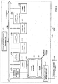
- FIG. 1 illustrates a voice and data modem ASIC 100 for use within a mobile wireless communications device such as a cellular telephone configured for use within a CDMA wireless communication system.
- the voice and data modem ASIC includes circuitry for handling telephony functions of the cellular telephone.
- ASIC includes a microprocessor 102 for controlling the voice and data modem functions.
- the microprocessor may be, for example, a reduced instructionset computing (RISC) microprocessor, such as the ARM 7TDMIJ microprocessor provided by Arm, IncJ.
- RISC reduced instructionset computing
- ARM 7TDMIJ microprocessor provided by Arm, IncJ.
- ARM 7TDMI and Arm, Inc. are both trademarks of Arm, Inc.
- other microprocessors are employed including, for example, complex instruction set computing (CISC) microprocessors.
- CISC complex instruction set computing
- peripheral components generally denoted 104, are provided within the ASIC for performing specific CDMA wireless telephony functions.
- a system bus 106 interconnects the microprocessor and the various CDMA peripheral components.
- the microprocessor controls the various CDMA peripheral components, via the system bus, to perform various functions directed to processing CDMA wireless communications such as converting CDMA signals received from a base station (not shown) into voice signals for outputting through a speaker of the cellular telephone or converting voice signals received from a microphone of the cellular telephone into CDMA signals for transmission to the base station.
- the microprocessor and the peripheral components store data or other information within either an internal memory system 108 formed on the ASIC or within an external memory system 110, which may comprise one or more SRAM, DRAM or flash memory chips mounted within the cellular telephone external to the ASIC.
- data or other information that needs to be accessed quickly is stored within the internal memory system for expedient access.
- Data that does not need to be retrieved as quickly is stored within the external memory system.
- the internal memory system includes a flash memory system 112 and an SRAM 113 integrated as a single memory system.
- the circuits of the single memory system and the circuits of the microprocessor and CDMA peripheral components are all integrated onto a single silicon die.
- the circuits of the single memory system are provided on one die and the microprocessor and peripheral CDMA components are provided on another die.
- the two separate silicon die are integrated within a single chip.
- an internal memory interface unit 115 interconnects the internal memory system with the microprocessor and the peripheral CDMA components via system bus 106.
- An external memory interface unit 117 interconnects the external memory system with the microprocessor and the peripheral CDMA components also via system bus 106.
- the flash memory of flash memory system 112 of the internalmemory system is used primarily for storing CDMA software code for use by the microprocessor or the CDMA peripheral components.
- the flash memory also includes a boot loader which is retrieved and run during an initial power-up operation by the microprocessor.
- the boot loader includes instructions for accessing and running other CDMA programs stored within the flash memory.
- the flash memory is also employed for providing non-volatile storage of data used in connection with the cellular telephone, such as storage of names, telephone numbers, addresses and the like. If the cellular telephone is configured as a smart phone to additionally perform the operations of a PDA, then the flash memory additionally stores data used by the PDA, such as meeting dates, calenders, schedules, voice memos, and the like. In general, any type of software or data which much be retained even while the cellular telephone is completed powered down is preferably stored within either the flash memory system embedded within ASIC or within the flash memory system, if any, provided within the external memory.
- Embedded SRAM 113 provides volatile storage of other types of data or software programs employed by the microprocessor or the peripheral components in connection with their functions.
- the various peripheral components may store the signals, or processed versions thereof, within the SRAM.
- the decoded symbols for voice are stored within the SRAM for subsequentprocessingby the vocoder.
- the external memory may also be employed as a volatile memory for storing data, particularly data which need not be accessed at high rates.
- a vocoder 114 for transmission of signals, a vocoder 114 is provided, which may include a DSP, for converting voice signals received through a microphone (not shown) into digitized symbols or other packetsof information.
- a CDMA encoder 116 encodes the symbols generated by the vocoder for error correction and detection purposes.
- a CDMA interleaver 118 interleaves the encoded signals to provide time diversity to thereby permit a reduction in transmission power.
- a CDMA modulator 120 modulates the interleaved signals for subsequent transmission via an antenna (not shown).
- a CDMA demodulator 122 demodulates the signals
- a deinterleaver 124 deinterleaves the signals so as to remove the effect of any previous interleaving
- a CDMA decoder 126 decodes signals to extract voice or data signals encoded therein.
- voice communications the decoded voice signals are output through a speaker (not shown) to the user of the telephone.
- data communications the decoded data signals are further processed by other components of the phone such as, for example, for display (on a display not shown) using a web browser program, email program or the like.
- FIG. 1 illustrates, among other features, an ASIC having an embedded flash and SRAM.
- the microprocessor and the flash and SRAM memory are thereby physically close to one another.
- data bus and control signals from the microprocessor to memory, and vice versa encounter less routing and capacitance delays as found on printed circuit boards when using off-chip memory.
- This improves overall memory access time and faster overall processing speeds.
- the flash and SRAM within ASIC, the overall size of the electronics of the cellular telephone can be reduced as compared with the systems requiring all memory to be external from the ASIC. This permits the cellular telephone to be configured using a slim and compactdesign.
- the flash memory and SRAM are embedded within the ASIC.
- the flash memory and SRAM. are provided off-chip, considerable power and energy is consumed toggling various input/output pin s required to access the flash memory and SRAM and signal traces on the printed circuit board.
- the system bus, the microprocessor, and the internal memory system are all configured to process 32-bit data paths.
- External flash and SRAM are typically accessed using only an 8-bit data path.
- 8-bit data path External flash and SRAM are typically accessed using only an 8-bit data path.
- the overall clock rates of the components of the ASIC can be reduced, thereby still further improving power consumption.
- 32-bit data path is not typically used because of pin and routing limitations.
- the provision of embedded flash memory and SRAM within the ASIC reduces the total number of chips required on the motherboard of the cellular telephone thereby increasing reliability as a result of simplified manufacturing processes.
- an embedded flash and SRAM memory within ASIC 100 provides numerous advantages.
- specific features of the flash and SRAM memories of the internal memory system will be described in greater detail. These features provide, for example, improved access time, improved protection from inadvertent rewrite operations, or the like.
- the embedded flash memory system includes a flash memory array 130 and a flash memory controller 132.
- Flash memory array 130 includes flash memory cells defining up to N different flash macros which, as will be described, can be independently accessed. In other words, a read operation can be performed on one of the flash macros while a write operation is performed on another of the flash macros.
- N is set at 4, permitting the flash memory to be subdivided into a total of four separate flash macros.
- a flash memory system bus 134 interconnects the flash memory array and the flash controller permitting the flash controller to access the flash memory array to perform read or write operations.
- all three components are configured to accommodate 32-bit data paths.
- Flash controller 132 includes a flash macro access unit 136 and various memory registers, including a programmable wait state register 138, a programmable password register 140 and a status register 142.
- the flash memory access unit uses information stored within the various registers to control access to the flash macros of the flash memory array. The information stored within the registers and the manner in which the information is used will be described in greater detail below.
- Flash memory access unit 136 includes a flash memory read unit 144 and a flash memory write unit 146.
- the read unit is used for reading data or software programs stored within the flash memory unit.
- the write unit is used for reprogramming portions of the flash memory to store new data or new programs.
- the read and flash write units provide a read while writing means for permitting a read operation to be performed on one of the flash macros while a write operation is simultaneously performed on another one of the flash macros.
- read unit 144 may perform a read operation on flash macro #1 while write unit performs a write operation on flash macro #2.
- a read operation is performed by forwarding a read command over flash bus 134 to flash memory array 130 specifying a particular memory address within the overall memory array.
- the address will specify a 32-bit memory address within the address spaces of flash macro #1.
- a write command is forwarded over the flash bus to the flash memory.
- the write command specifies an address within the flash macro and additionally specifies the data to be stored therein.
- the write command will provide 32 bits of data along with the memory address. Also, as will be described below, a write operation is only performed if a correct password is received from the microprocessor or peripheral component as part of the write command.
- Flash memory write operations take a substantially greater amount of time than a flash read operation.
- a read operation for example,may be performed within only a single clock cycle.
- a write operation may require hundreds of clock cycles. Accordingly, a very large number of individual read operations may be performed while a single write operation is being performed.
- Read operations are performed on any of the flash macros other than the macro subject to the write operation. If a read request is received from the microprocessor specifying an address within the flash macro being currently subject to a write operation, the read operation is deferred by the flash macro access unit until the write operation has completed. Additionally, the flash memory access unit forwards a signal to the microprocessor controlling the processor to suspend operation pending completion of the write operation. This may be achieved using an interrupt signal or other conventional technique. In other implementations, such as in an implementation employing a microprocessor capable of a speculative processing, it may be desirable to permit the microprocessor to continue to operate while the write operation is performed.
- the read while write mechanism permits faster read access times to be achieved, on the average, because read operations need not be deferred until completion of a pending write operation unless issued to the same flash macro.
- the overall system is more efficient, either permitting the system to perform more operations within a given period of time or permitting the system to be run at a generally lower clock rate, thus reducing power consumption.
- the flash memory access unit additionally includes an erase unit 147 for erasing portions of the flash memory.
- the erase unit receives an erase command from the microprocessor or other component specifying a beginning address and further specifying the amount of data to be erased.
- the erase to the command may specify erasure of either a single word (32 bits), an entire page, or the entire flash memory array.
- an erase operation is only performed if a correct password is received from the microprocessor or peripheral component as part of the erase command.
- amass erase all other read or write requests to the flash memory are stalled pending completion of the mass erase operation.
- all flash memory operations are also stalled when a page of the flash memory is erased, even if the operation is to be performed to a flash macro separate from the page being erased.
- flash memory operations are permitted to other flash macros not affected by the page being erased.
- an erase operation may need to be performed prior to any write (or program) operation. More specifically, if the flash memory is configured such that a write operation can only cause a "one" bit to change to a "zero" bit, then an erase operation will need to be performed to the word or words being written to prior to the actual write operation.
- flash memory write unit 146 upon receiving a write command, first controls erase unit 147 to erase the word or words subject to the write operation before performing the write operation.
- write unit 146 does not automatically perform an erase operation prior to a write operation.
- software designers must ensure that software accessing the flash memory performs erase operations prior to write operations.
- the flash memory access unit also includes a memory swap unit 149 for use in swapping high and low memory portions of the overall memory address phase of memory array 130.
- the operation of the memory swap unit will be described in greater detail below in connection with FIG. 5 .
- FIG. 3 illustrates wait state memory register 138 for flash bus wait states for use with different portions of the flash memory array.
- the wait state memory register includes M separate storage registers for storing wait state values associated with M separate portions of the flash memory array.
- M is set to N such that there is one separate wait state register per flash macro.
- N is set to four and M is set to 16.
- Each wait state register stores a wait state value for use during read operationsto any memory address within a corresponding portion of the memory array.
- the wait state specifies the number of cycles of the flash memory bus that the flash memory access unit must wait until retrieval of data via a read operation.
- the flash memory access unit accesses the flash bus during the clock cycle immediately subsequent to a clock cycle in which a read operation was asserted to the flash array. If the wait state is set to 3, then the flash memory access unit waits three clock cycles subsequent to the assertion of a read operation.
- Different wait state values can be provided for different portions of flash memory array to accommodate differing degrees of degradation of the flash memory arrays. Briefly, the more often a flash cell is written to, the slower the flash cell responds to subsequent read operations. With different portions of the flash array storing different types of data or programs, different degrees of read time degradation occur. More specifically, portions of the flash memory that are frequently rewritten, such as portions used to store voice memos, are subject to a greater amount of degradation than portions of flash memory that are re-written infrequently, such as portions storing the boot loader. (In an implementation described below, the boot loader is swapped in and out of high memory resulting in some degree of degradation to the memory cells used to store the boot loader.)
- a separate wait state value is stored within the wait state register for each portion of memory depending upon the degree of expected degradation of that memory. For portions of memory that are expected to be re-programmed only infrequently, a wait state of zero is pre-programmed within the corresponding wait state memory register. For portions of the array that are expected to be reprogrammed frequently, a wait state value of 3 is preferably pre-programmed. The amount of re-programming that is expected is determined in advance based upon the overall system hardware and software design. Thus, if certain hardware and software components that frequently write to flash memory, such as voice memo components, are designed to use only flash macro #3, then the wait state for flash macro #3 is preset to 3.
- a wait state of 0 is pre-set for flash macro #1; a wait state of 1 is pre-set for flash macro #2; a wait state of 2 is pre-set for flash macro #3 and so on.
- Software and hardware designers are instructed to design systems to write to the flash macros based upon the expected write frequency.
- Designers developing hardware or software that make frequent writes to flash memory will configure their systems to write to flash macro #4.
- Designers developing hardware or software that writes to flash memory only infrequently will configure their systems to write to flash macro #1.
- the flash memory access unit is configured to track the number of write operations performed to each flash macro and to selectively increase the number of wait states associated accordingly.
- the wait state registers are all preset to zero when the cellular telephone is initially manufactured.
- the individual values stored within the wait state registers are selectively reset to 1, then perhaps 2, then 3 or more.
- the wait state registers may be a year or two before any of the wait state registers are reset from zero to 1 and none may ever reach a wait state value of 3. In other cases, the values may need to be reset more frequently.
- an even greater number of wait state values are provided including, for example, wait state values from zero to 10.
- the total number of wait state values and the number of reprogramming operations performed before the number of wait states is increased depends greatly upon the particular flash memory array, the flash bus, and the flash controller as well as the overall frequency of the clock used to control the various components. However, for each choice of components and for each choice of clock signal, routine experimentation may be performed to determine acceptable or optimal values for the wait state values and to determine how frequently the wait state values need to be incremented. In any case, by providing programmable wait state values, average memory access times can be reduced thereby providing for either greater processing speed or permitting use of a slower clock to achieve similar processing speeds.
- FIG. 4 illustrates flash memory password register 140 for storing passwords associated with different portions of the flash memory array.
- the flash memory password register stores P passwords, each one associated with a corresponding portion of the flash memory array.
- P is set to 16.
- P may be set to the same value of M.
- Each individual password register stores a unique password required before a write or erase operation can be performed to the corresponding portion of the memory array.
- each write command received from the microprocessor or other component of the ASIC specifies a password, along with a memory address and the data to be written to that address.
- Each erase command also specifies a password, along with an identification of the memory addresses to be erased.
- write unit 146 FIG.
- the write unit 2 compares the password received within the write command with the password stored within the password register for the memory address specified by the write command. If the passwords match, the write unit proceeds to perform the write command by forwarding the write operation to the flash memory. If the passwords do not match, the write unit forwards an error signal back to the component issuing the write command informing the component that the write command could not be performed because of an invalid password. Erase commands are handled n the same manner.
- password protection is provided.
- Password protection is provided, in part, to prevent inadvertent erasure or reprogramming of portions of the flash memory, perhaps as a result of a software bug or the like. In this regard, it is fairly unlikely that an inadvertent write or erase command would include the correct password.
- password protection also helps prevent one peripheral component from inadvertently writing into a memory area reserved for another component. For example, the vocoder may read or write only from flash macro #2.
- Other password protocols may be alternatively provided. For example, rather than associating a different password with different portions of memory, different passwords may be directly associated with different issuing components.
- a first password may be associated with commands received from the microprocessor, whereas a second password is associated with commands received from the vocoder.
- each device can potentially read to or write from any of the flash macros, but the risk of inadvertent write operations is minimized nevertheless.
- Each password may be, for example, a unique binary sequence of 16 bits. By providing password protection, the loss of important data is avoided, such as loss of phone numbers for police, fire or the like. Also, the risk that portions of the CDMA code stored within the flash memory might be corrupted is reduced. In an extreme case, corruption of one or more of the CDMA programs stored within the flash memory could result in failure of the overall cellular telephone, requiring the customer to return the cellular telephone for replacement or service.
- the user may be able to record particular passwords for use with data stored by the user. For example, if one of the flash macros is used exclusively for storing voice memos, the user may input a unique password via the keypad of the cellular telephone preventing unauthorized access to the voice memo by another user of the telephone. Likewise, particular portions of memory for storing phone numbers, addresses and the like may have a user-entered a password associated therewith to prevent unauthorized access as well. As can be appreciated, a wide variety of different password scenarios may be provided consistent with the general principles of the invention.
- a portion of the flash memory array may be employed to store a boot loader.
- a separate additional password register 150 is provided for the portion of memory storing the boot loader. Hence, no write or erase command affecting the portion of memory storing the boot loader is performed unless that command additionally provides the separate boot loader password. This, therefore, provides an additional level of password protection to the critical boot loader for minimizing risk that the boot loader will be inadvertently corrupted.
- FIG. 5 illustrates flash memory status register 142 for storing the status of the flash macros of the flash memory array.
- the status register includes N individual memory elements for separately storing the status of each of the N flash macros.
- Each status register specifies, among other possible features, whether the corresponding flash macro is subject to a current pending read or write operation. Additionally, the status register may further specify the software or hardware entity performing the read or write operation.
- the microprocessor can determine, using appropriate prioritization tables maintained by the microprocessor, whether a newly requested flash memory operation is of higher priority and, if so, the microprocessor may interrupt the flash controller causing it to abort the read or write operation to permit the higher priority flash memory operation to be immediately performed.
- the status registers may further store any indication of the status of a current read or write operation.
- the status register may record the time at which a read or write command was forwarded to the flash memory array.
- the microprocessor can access the time value and determine therefrom when the command will likely be completed. If a write operation typically takes 100 clock cycles, the microprocessor can determine whether the pending write command was only recently issued or whether it has almost been completed. This may permit the microprocessor to determine whether to interrupt the flash controller to issue a higher priority write operation.
- the status register may specify the number of wait cycles used in connection with the particular read operation.
- a wide variety of status information can be stored within a status register depending upon the preprogramming of the system. In general, a status information is provided to improve the overall efficiency of the system to permit a greater number of operations to be performed within a given period of time or to permit a lower clock rate to be used while still achieving the same number of operations per second.
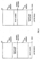
- FIG. 6 illustrates the operation of the memory swap unit 149 ( FIG. 2 ) which operates to swap high and low memory portions of an overall memory address space 152 of memory array 130 (also FIG. 2 ).
- a boot loader is initially stored at a lowest memory address of the memory space, e.g., address 0X00.
- Main software programs are stored beginning at a high memory address such as 0X05800000.
- the boot loader includes commands specifying which of the main software programs within the flash memory need to be run as part of a power-up or reset operation.
- the memory swap unit swaps high and low memory.
- the primary flash software programs are stored beginning at memory location 0X0.
- the boot loader is stored at a high memory address such as 0X05800000. Hence, a jump to low memory now allows entry into the main software of the flash macros. This permits the main flash software to be accessed more expediently. If thereafter, the cellular telephone is turned off and then turned back on again or if some other reset operation is performed, the memory addresses are again swapped such that the boot loader resides at the lowest memory address to permit proper initial operation of the boot loader.
Landscapes
- Engineering & Computer Science (AREA)
- Computer Security & Cryptography (AREA)
- Read Only Memory (AREA)
- Memory System (AREA)
- Storage Device Security (AREA)
- Semiconductor Memories (AREA)
- Techniques For Improving Reliability Of Storages (AREA)
- Non-Volatile Memory (AREA)
Applications Claiming Priority (2)
| Application Number | Priority Date | Filing Date | Title |
|---|---|---|---|
| US09/465,665 US6407949B1 (en) | 1999-12-17 | 1999-12-17 | Mobile communication device having integrated embedded flash and SRAM memory |
| EP00986483A EP1238393B1 (en) | 1999-12-17 | 2000-12-14 | Mobile communication device having integrated embedded flash and sram memory |
Related Parent Applications (1)
| Application Number | Title | Priority Date | Filing Date |
|---|---|---|---|
| EP00986483A Division EP1238393B1 (en) | 1999-12-17 | 2000-12-14 | Mobile communication device having integrated embedded flash and sram memory |
Publications (2)
| Publication Number | Publication Date |
|---|---|
| EP1710806A1 EP1710806A1 (en) | 2006-10-11 |
| EP1710806B1 true EP1710806B1 (en) | 2016-02-03 |
Family
ID=23848684
Family Applications (4)
| Application Number | Title | Priority Date | Filing Date |
|---|---|---|---|
| EP06015159A Withdrawn EP1713080A1 (en) | 1999-12-17 | 2000-12-14 | Mobile communication device having integrated embedded flash and SRAM |
| EP00986483A Expired - Lifetime EP1238393B1 (en) | 1999-12-17 | 2000-12-14 | Mobile communication device having integrated embedded flash and sram memory |
| EP06015158.6A Expired - Lifetime EP1713079B1 (en) | 1999-12-17 | 2000-12-14 | Mobile communication device having integrated embedded flash and sram memory |
| EP06015160.2A Expired - Lifetime EP1710806B1 (en) | 1999-12-17 | 2000-12-14 | Mobile communication device having integrated embedded flash and sram memory |
Family Applications Before (3)
| Application Number | Title | Priority Date | Filing Date |
|---|---|---|---|
| EP06015159A Withdrawn EP1713080A1 (en) | 1999-12-17 | 2000-12-14 | Mobile communication device having integrated embedded flash and SRAM |
| EP00986483A Expired - Lifetime EP1238393B1 (en) | 1999-12-17 | 2000-12-14 | Mobile communication device having integrated embedded flash and sram memory |
| EP06015158.6A Expired - Lifetime EP1713079B1 (en) | 1999-12-17 | 2000-12-14 | Mobile communication device having integrated embedded flash and sram memory |
Country Status (12)
| Country | Link |
|---|---|
| US (2) | US6407949B1 (ja) |
| EP (4) | EP1713080A1 (ja) |
| JP (5) | JP4795598B2 (ja) |
| KR (1) | KR20030011067A (ja) |
| CN (1) | CN1411601A (ja) |
| AT (1) | ATE339764T1 (ja) |
| AU (1) | AU2271301A (ja) |
| CA (4) | CA2704894A1 (ja) |
| DE (1) | DE60030765T2 (ja) |
| ES (1) | ES2269213T3 (ja) |
| HK (1) | HK1052248A1 (ja) |
| WO (1) | WO2001045106A2 (ja) |
Families Citing this family (46)
| Publication number | Priority date | Publication date | Assignee | Title |
|---|---|---|---|---|
| JP2001025053A (ja) | 1999-07-09 | 2001-01-26 | Mitsubishi Electric Corp | 携帯電話のメモリシステム |
| US6563746B2 (en) * | 1999-11-09 | 2003-05-13 | Fujitsu Limited | Circuit for entering/exiting semiconductor memory device into/from low power consumption mode and method of controlling internal circuit at low power consumption mode |
| US6407949B1 (en) * | 1999-12-17 | 2002-06-18 | Qualcomm, Incorporated | Mobile communication device having integrated embedded flash and SRAM memory |
| US6785806B1 (en) | 1999-12-30 | 2004-08-31 | Intel Corporation | Bios having macro/effector pairs for hardware initialization |
| PL355475A1 (en) * | 2000-02-21 | 2004-05-04 | Trek 2000 International Ltd. | A portable data storage device |
| JP2001249471A (ja) | 2000-03-07 | 2001-09-14 | Fuji Denki Gazo Device Kk | 電子写真用感光体 |
| US6741978B1 (en) * | 2000-04-12 | 2004-05-25 | Intel Corporation | Accessing file data stored in non-volatile re-programmable semiconductor memories |
| JP4840553B2 (ja) * | 2001-07-31 | 2011-12-21 | 日本電気株式会社 | 無線通信機と、そのブートプログラム書き換え方法及びプログラム |
| US20030046575A1 (en) * | 2001-08-30 | 2003-03-06 | International Business Machines Corporation | Digital identity information cards |
| TW538338B (en) * | 2001-12-19 | 2003-06-21 | Yi-Lang Jang | Data protection device using addresses |
| GB2385956B (en) * | 2002-03-01 | 2004-06-02 | 3Com Corp | Key based register locking mechanism |
| EP1345236B1 (en) * | 2002-03-14 | 2011-05-11 | STMicroelectronics Srl | A non-volatile memory device |
| CA2380762A1 (en) * | 2002-04-04 | 2003-10-04 | Intrinsyc Software, Inc. | Internet-enabled device provisioning, upgrade and recovery mechanism |
| US8108588B2 (en) * | 2003-04-16 | 2012-01-31 | Sandisk Il Ltd. | Monolithic read-while-write flash memory device |
| US7171288B2 (en) * | 2003-10-06 | 2007-01-30 | Invacare Corporation | Method and apparatus for reprogramming a programmed controller of a power driven wheelchair |
| US7210002B2 (en) * | 2003-11-19 | 2007-04-24 | Qualcomm Incorporated | System and method for operating dual bank read-while-write flash |
| KR100533683B1 (ko) * | 2004-02-03 | 2005-12-05 | 삼성전자주식회사 | 플래시 메모리의 데이터 관리 장치 및 방법 |
| US20050177754A1 (en) * | 2004-02-09 | 2005-08-11 | Board Of Control Of Michigan Technological University | Password management peripheral system and method |
| JP2007526724A (ja) * | 2004-03-04 | 2007-09-13 | クゥアルコム・インコーポレイテッド | ワイアレス・ネットワークにおける低データ・レート・トラフィックの早期打ち切り |
| JP4768237B2 (ja) * | 2004-06-25 | 2011-09-07 | 株式会社東芝 | 携帯可能電子装置及び携帯可能電子装置の制御方法 |
| JP4460967B2 (ja) * | 2004-07-23 | 2010-05-12 | 株式会社東芝 | メモリカード、不揮発性半導体メモリ、及び半導体メモリの制御方法 |
| US20060069849A1 (en) * | 2004-09-30 | 2006-03-30 | Rudelic John C | Methods and apparatus to update information in a memory |
| US20060215437A1 (en) * | 2005-03-28 | 2006-09-28 | Trika Sanjeev N | Recovering from memory imprints |
| KR20080032035A (ko) | 2005-05-25 | 2008-04-14 | 엔엑스피 비 브이 | 휴대용 전자 단말기 및 휴대용 전자 단말기 관리 방법 |
| JP2007011872A (ja) * | 2005-07-01 | 2007-01-18 | Toshiba Corp | メモリカードとその制御方法 |
| JP2009503656A (ja) * | 2005-07-21 | 2009-01-29 | クレブエックス・リミテッド・ライアビリティ・カンパニー | メモリロックシステム |
| JP2007128633A (ja) | 2005-10-07 | 2007-05-24 | Matsushita Electric Ind Co Ltd | 半導体記憶装置及びこれを備えた送受信システム |
| US7598166B2 (en) * | 2006-09-08 | 2009-10-06 | International Business Machines Corporation | Dielectric layers for metal lines in semiconductor chips |
| US7941587B2 (en) * | 2007-09-17 | 2011-05-10 | Cadence Design Systems, Inc | Programmable sequence generator for a flash memory controller |
| KR100971532B1 (ko) * | 2008-05-27 | 2010-07-21 | 삼성전자주식회사 | 구동 트랜지스터를 포함하는 반도체 소자 |
| US7761635B1 (en) * | 2008-06-20 | 2010-07-20 | Tableau, Llc | Bridge device access system |
| US8209439B2 (en) * | 2008-08-25 | 2012-06-26 | Sandisk Il Ltd. | Managing multiple concurrent operations with various priority levels in a local storage device |
| US20100174913A1 (en) * | 2009-01-03 | 2010-07-08 | Johnson Simon B | Multi-factor authentication system for encryption key storage and method of operation therefor |
| US9286493B2 (en) * | 2009-01-07 | 2016-03-15 | Clevx, Llc | Encryption bridge system and method of operation thereof |
| DE102009014995A1 (de) * | 2009-03-26 | 2010-09-30 | Giesecke & Devrient Gmbh | Sicherer Speicherzugriff auf einem portablen Datenträger |
| US8572344B2 (en) * | 2009-05-04 | 2013-10-29 | Hewlett-Packard Development Company, L.P. | Storage device erase command having a control field controllable by a requestor device |
| GB2491774B (en) * | 2010-04-12 | 2018-05-09 | Hewlett Packard Development Co | Authenticating clearing of non-volatile cache of storage device |
| US8495601B2 (en) | 2010-06-09 | 2013-07-23 | Lear Corporation | Shared memory architecture |
| US8539472B2 (en) | 2010-06-09 | 2013-09-17 | Lear Corporation | Method and system of updating shared memory |
| US8570809B2 (en) | 2011-12-02 | 2013-10-29 | Cypress Semiconductor Corp. | Flash memory devices and systems |
| TWI520148B (zh) * | 2012-07-05 | 2016-02-01 | 慧榮科技股份有限公司 | 記憶體裝置和記憶體控制方法 |
| CN102855922A (zh) * | 2012-09-05 | 2013-01-02 | 南京智达康无线通信科技股份有限公司 | 一种在Flash中记录死机信息的方法 |
| US10185331B2 (en) * | 2013-03-11 | 2019-01-22 | Ice Computer, Inc. | Modular computer and thermal management |
| CN105678117B (zh) * | 2014-11-19 | 2019-12-20 | 比亚迪股份有限公司 | 单片机闪存程序的安全性保护方法及保护装置及单片机 |
| US10146704B2 (en) * | 2016-02-16 | 2018-12-04 | Dell Products L.P. | Volatile/non-volatile memory device access provisioning system |
| US10185664B1 (en) * | 2017-06-30 | 2019-01-22 | Vmware, Inc. | Method for switching address spaces via an intermediate address space |
Family Cites Families (33)
| Publication number | Priority date | Publication date | Assignee | Title |
|---|---|---|---|---|
| JPH02235156A (ja) | 1989-03-08 | 1990-09-18 | Canon Inc | 情報処理装置 |
| US5245572A (en) * | 1991-07-30 | 1993-09-14 | Intel Corporation | Floating gate nonvolatile memory with reading while writing capability |
| US5473775A (en) * | 1991-10-11 | 1995-12-05 | Kabushiki Kaisha Toshiba | Personal computer using flash memory as BIOS-ROM |
| JP2971267B2 (ja) * | 1991-10-11 | 1999-11-02 | 株式会社東芝 | フラッシュメモリをbios−romとして使用したパーソナルコンピュータ |
| JP3152535B2 (ja) * | 1993-03-18 | 2001-04-03 | 富士通株式会社 | データ処理装置 |
| US5463766A (en) * | 1993-03-22 | 1995-10-31 | Dell Usa, L.P. | System and method for loading diagnostics routines from disk |
| US5522076A (en) * | 1993-05-13 | 1996-05-28 | Kabushiki Kaisha Toshiba | Computer system having BIOS (basic input/output system)-ROM (Read Only Memory) writing function |
| US5592641A (en) * | 1993-06-30 | 1997-01-07 | Intel Corporation | Method and device for selectively locking write access to blocks in a memory array using write protect inputs and block enabled status |
| JP3464271B2 (ja) * | 1994-04-12 | 2003-11-05 | 三菱電機株式会社 | 不揮発性半導体記憶装置 |
| FR2719939A1 (fr) | 1994-05-11 | 1995-11-17 | Sgs Thomson Microelectronics | Mémoire non volatile modifiable électriquement à interface de commande. |
| JP3739102B2 (ja) * | 1994-07-07 | 2006-01-25 | 富士通株式会社 | 不揮発性半導体記憶装置 |
| JPH0844628A (ja) * | 1994-08-03 | 1996-02-16 | Hitachi Ltd | 不揮発性メモリ、およびそれを用いたメモリカード、情報処理装置、ならびに不揮発性メモリのソフトウェアライトプロテクト制御方法 |
| DE19536206A1 (de) * | 1994-09-30 | 1996-04-04 | Samsung Electronics Co Ltd | Intelligente Karte |
| US5978941A (en) * | 1995-03-15 | 1999-11-02 | Hitachi, Ltd. | Semiconductor memory device having deterioration determining function |
| JPH0969067A (ja) * | 1995-08-31 | 1997-03-11 | Hitachi Ltd | 半導体記憶装置、及びデータ処理装置 |
| JPH09114768A (ja) * | 1995-10-20 | 1997-05-02 | Toshiba Corp | コンピュータシステム |
| KR100359414B1 (ko) * | 1996-01-25 | 2003-01-24 | 동경 엘렉트론 디바이스 주식회사 | 데이타독출/기록방법및그를이용한메모리제어장치및시스템 |
| US6148360A (en) | 1996-09-20 | 2000-11-14 | Intel Corporation | Nonvolatile writeable memory with program suspend command |
| US5937063A (en) * | 1996-09-30 | 1999-08-10 | Intel Corporation | Secure boot |
| US5987581A (en) * | 1997-04-02 | 1999-11-16 | Intel Corporation | Configurable address line inverter for remapping memory |
| US5930826A (en) * | 1997-04-07 | 1999-07-27 | Aplus Integrated Circuits, Inc. | Flash memory protection attribute status bits held in a flash memory array |
| JPH1196078A (ja) * | 1997-09-24 | 1999-04-09 | Matsushita Electric Ind Co Ltd | 半導体メモリ装置 |
| EP0905704B1 (en) | 1997-09-24 | 2010-03-31 | STMicroelectronics S.r.l. | Sectored semiconductor memory device with configurable memory sector addresses |
| US5822244A (en) * | 1997-09-24 | 1998-10-13 | Motorola, Inc. | Method and apparatus for suspending a program/erase operation in a flash memory |
| JPH11110293A (ja) * | 1997-09-29 | 1999-04-23 | Mitsubishi Electric Corp | 不揮発性メモリ制御回路 |
| JPH11110294A (ja) * | 1997-10-01 | 1999-04-23 | Toshiba Corp | マイクロコンピュータ及び情報処理装置 |
| WO1999033057A1 (en) | 1997-12-23 | 1999-07-01 | Macronix International Co., Ltd. | Technique for increasing endurance of integrated circuit memory |
| US6088264A (en) * | 1998-01-05 | 2000-07-11 | Intel Corporation | Flash memory partitioning for read-while-write operation |
| EP1058930B1 (en) | 1998-01-06 | 2009-06-03 | Macronix International Co., Ltd. | A memory supporting multiple address protocols |
| JP3544859B2 (ja) * | 1998-05-11 | 2004-07-21 | 富士通株式会社 | 不揮発性半導体メモリを使用した2次記憶装置 |
| US6205548B1 (en) * | 1998-07-31 | 2001-03-20 | Intel Corporation | Methods and apparatus for updating a nonvolatile memory |
| US6356987B1 (en) * | 1999-03-10 | 2002-03-12 | Atmel Corporation | Microprocessing device having programmable wait states |
| US6407949B1 (en) * | 1999-12-17 | 2002-06-18 | Qualcomm, Incorporated | Mobile communication device having integrated embedded flash and SRAM memory |
-
1999
- 1999-12-17 US US09/465,665 patent/US6407949B1/en not_active Expired - Lifetime
-
2000
- 2000-12-14 CA CA2704894A patent/CA2704894A1/en not_active Abandoned
- 2000-12-14 EP EP06015159A patent/EP1713080A1/en not_active Withdrawn
- 2000-12-14 CN CN00817327A patent/CN1411601A/zh active Pending
- 2000-12-14 CA CA2704892A patent/CA2704892A1/en not_active Abandoned
- 2000-12-14 JP JP2001545312A patent/JP4795598B2/ja not_active Expired - Lifetime
- 2000-12-14 CA CA002393143A patent/CA2393143A1/en not_active Abandoned
- 2000-12-14 EP EP00986483A patent/EP1238393B1/en not_active Expired - Lifetime
- 2000-12-14 WO PCT/US2000/034216 patent/WO2001045106A2/en active IP Right Grant
- 2000-12-14 DE DE60030765T patent/DE60030765T2/de not_active Expired - Lifetime
- 2000-12-14 CA CA2704893A patent/CA2704893A1/en not_active Abandoned
- 2000-12-14 AU AU22713/01A patent/AU2271301A/en not_active Abandoned
- 2000-12-14 EP EP06015158.6A patent/EP1713079B1/en not_active Expired - Lifetime
- 2000-12-14 ES ES00986483T patent/ES2269213T3/es not_active Expired - Lifetime
- 2000-12-14 AT AT00986483T patent/ATE339764T1/de not_active IP Right Cessation
- 2000-12-14 EP EP06015160.2A patent/EP1710806B1/en not_active Expired - Lifetime
- 2000-12-14 KR KR1020027007785A patent/KR20030011067A/ko not_active Application Discontinuation
-
2001
- 2001-03-26 US US09/818,186 patent/US6392925B2/en not_active Expired - Lifetime
-
2003
- 2003-06-20 HK HK03104445.0A patent/HK1052248A1/zh unknown
-
2011
- 2011-04-18 JP JP2011092137A patent/JP5123410B2/ja not_active Expired - Lifetime
-
2012
- 2012-02-07 JP JP2012024017A patent/JP2012141994A/ja not_active Withdrawn
- 2012-02-07 JP JP2012024016A patent/JP5453471B2/ja not_active Expired - Lifetime
-
2014
- 2014-04-03 JP JP2014077098A patent/JP5801436B2/ja not_active Expired - Lifetime
Also Published As
| Publication number | Publication date |
|---|---|
| ATE339764T1 (de) | 2006-10-15 |
| CA2704892A1 (en) | 2001-06-21 |
| JP2012141993A (ja) | 2012-07-26 |
| DE60030765T2 (de) | 2007-09-13 |
| WO2001045106A3 (en) | 2002-01-10 |
| EP1713080A1 (en) | 2006-10-18 |
| US6407949B1 (en) | 2002-06-18 |
| JP5123410B2 (ja) | 2013-01-23 |
| JP5801436B2 (ja) | 2015-10-28 |
| EP1713079B1 (en) | 2018-03-21 |
| EP1710806A1 (en) | 2006-10-11 |
| CN1411601A (zh) | 2003-04-16 |
| KR20030011067A (ko) | 2003-02-06 |
| US20010036109A1 (en) | 2001-11-01 |
| DE60030765D1 (de) | 2006-10-26 |
| JP4795598B2 (ja) | 2011-10-19 |
| JP5453471B2 (ja) | 2014-03-26 |
| JP2003517168A (ja) | 2003-05-20 |
| CA2393143A1 (en) | 2001-06-21 |
| AU2271301A (en) | 2001-06-25 |
| EP1713079A1 (en) | 2006-10-18 |
| JP2014160485A (ja) | 2014-09-04 |
| JP2011192290A (ja) | 2011-09-29 |
| HK1052248A1 (zh) | 2003-09-05 |
| ES2269213T3 (es) | 2007-04-01 |
| US6392925B2 (en) | 2002-05-21 |
| EP1238393A2 (en) | 2002-09-11 |
| CA2704893A1 (en) | 2001-06-21 |
| CA2704894A1 (en) | 2001-06-21 |
| WO2001045106A2 (en) | 2001-06-21 |
| JP2012141994A (ja) | 2012-07-26 |
| EP1238393B1 (en) | 2006-09-13 |
Similar Documents
| Publication | Publication Date | Title |
|---|---|---|
| EP1710806B1 (en) | Mobile communication device having integrated embedded flash and sram memory | |
| US7093064B2 (en) | Programming suspend status indicator for flash memory | |
| US7061804B2 (en) | Robust and high-speed memory access with adaptive interface timing | |
| KR100393619B1 (ko) | 휴대 단말기의 메모리 장치 및 그 제어방법 | |
| US7245527B2 (en) | Nonvolatile memory system using magneto-resistive random access memory (MRAM) | |
| US6260103B1 (en) | Read-while-write memory including fewer verify sense amplifiers than read sense amplifiers | |
| US7149844B2 (en) | Non-volatile memory device | |
| JPH1050078A (ja) | 電気的に消去およびプログラムが可能なリード・オンリ・メモリの消去およびプログラミング保護方法および装置 | |
| WO2009105055A1 (en) | Memory area protection system and methods | |
| US6883078B2 (en) | Microcomputer with reduced memory usage and associated method | |
| KR20110078171A (ko) | 부팅가능한 휘발성 메모리 장치와 그를 구비한 메모리 모듈 및 프로세싱 시스템, 및 그를 이용한 프로세싱 시스템 부팅 방법 | |
| US20040153601A1 (en) | General purpose lines for memory write protection | |
| WO2001045112A1 (en) | Mobile communication device having flash memory system with word line buffer |
Legal Events
| Date | Code | Title | Description |
|---|---|---|---|
| PUAI | Public reference made under article 153(3) epc to a published international application that has entered the european phase |
Free format text: ORIGINAL CODE: 0009012 |
|
| 17P | Request for examination filed |
Effective date: 20060720 |
|
| AC | Divisional application: reference to earlier application |
Ref document number: 1238393 Country of ref document: EP Kind code of ref document: P |
|
| AK | Designated contracting states |
Kind code of ref document: A1 Designated state(s): AT BE CH CY DE DK ES FI FR GB GR IE IT LI LU MC NL PT SE TR |
|
| AX | Request for extension of the european patent |
Extension state: AL LT LV MK RO SI |
|
| RIN1 | Information on inventor provided before grant (corrected) |
Inventor name: SIMMONDS, STEPHEN Inventor name: ELHUS-SEINI, JALALC/O QUALCOMM INCORPORATED Inventor name: KHAN, SAFI Inventor name: JHA, SANJAYC/O QUALCOMM INCORPORATED Inventor name: YU, NICHOLAS, K. |
|
| RIN1 | Information on inventor provided before grant (corrected) |
Inventor name: ELHUS-SEINI, JALALC/O QUALCOMM INCORPORATED Inventor name: SIMMONDS, STEPHEN Inventor name: JHA, SANJAYC/O QUALCOMM INCORPORATED Inventor name: YU, NICHOLAS, K.C/O QUALCOMM INCORPORATED Inventor name: KHAN, SAFI |
|
| 17Q | First examination report despatched |
Effective date: 20070213 |
|
| AKX | Designation fees paid |
Designated state(s): AT BE CH CY DE DK ES FI FR GB GR IE IT LI LU MC NL PT SE TR |
|
| GRAP | Despatch of communication of intention to grant a patent |
Free format text: ORIGINAL CODE: EPIDOSNIGR1 |
|
| RIC1 | Information provided on ipc code assigned before grant |
Ipc: G11C 16/10 20060101ALI20150624BHEP Ipc: G11C 7/24 20060101AFI20150624BHEP Ipc: G11C 16/26 20060101ALI20150624BHEP Ipc: G11C 16/22 20060101ALI20150624BHEP |
|
| INTG | Intention to grant announced |
Effective date: 20150710 |
|
| RIN1 | Information on inventor provided before grant (corrected) |
Inventor name: ELHUS-SEINI, JALAL Inventor name: YU, NICHOLAS, K. Inventor name: JHA, SANJAY Inventor name: KHAN, SAFI Inventor name: SIMMONDS, STEPHEN |
|
| GRAS | Grant fee paid |
Free format text: ORIGINAL CODE: EPIDOSNIGR3 |
|
| GRAA | (expected) grant |
Free format text: ORIGINAL CODE: 0009210 |
|
| AC | Divisional application: reference to earlier application |
Ref document number: 1238393 Country of ref document: EP Kind code of ref document: P |
|
| AK | Designated contracting states |
Kind code of ref document: B1 Designated state(s): AT BE CH CY DE DK ES FI FR GB GR IE IT LI LU MC NL PT SE TR |
|
| REG | Reference to a national code |
Ref country code: GB Ref legal event code: FG4D |
|
| REG | Reference to a national code |
Ref country code: AT Ref legal event code: REF Ref document number: 774028 Country of ref document: AT Kind code of ref document: T Effective date: 20160215 Ref country code: CH Ref legal event code: EP |
|
| REG | Reference to a national code |
Ref country code: IE Ref legal event code: FG4D |
|
| REG | Reference to a national code |
Ref country code: DE Ref legal event code: R096 Ref document number: 60049194 Country of ref document: DE |
|
| REG | Reference to a national code |
Ref country code: NL Ref legal event code: MP Effective date: 20160203 |
|
| REG | Reference to a national code |
Ref country code: AT Ref legal event code: MK05 Ref document number: 774028 Country of ref document: AT Kind code of ref document: T Effective date: 20160203 |
|
| PG25 | Lapsed in a contracting state [announced via postgrant information from national office to epo] |
Ref country code: FI Free format text: LAPSE BECAUSE OF FAILURE TO SUBMIT A TRANSLATION OF THE DESCRIPTION OR TO PAY THE FEE WITHIN THE PRESCRIBED TIME-LIMIT Effective date: 20160203 Ref country code: ES Free format text: LAPSE BECAUSE OF FAILURE TO SUBMIT A TRANSLATION OF THE DESCRIPTION OR TO PAY THE FEE WITHIN THE PRESCRIBED TIME-LIMIT Effective date: 20160203 Ref country code: GR Free format text: LAPSE BECAUSE OF FAILURE TO SUBMIT A TRANSLATION OF THE DESCRIPTION OR TO PAY THE FEE WITHIN THE PRESCRIBED TIME-LIMIT Effective date: 20160504 Ref country code: IT Free format text: LAPSE BECAUSE OF FAILURE TO SUBMIT A TRANSLATION OF THE DESCRIPTION OR TO PAY THE FEE WITHIN THE PRESCRIBED TIME-LIMIT Effective date: 20160203 |
|
| PG25 | Lapsed in a contracting state [announced via postgrant information from national office to epo] |
Ref country code: PT Free format text: LAPSE BECAUSE OF FAILURE TO SUBMIT A TRANSLATION OF THE DESCRIPTION OR TO PAY THE FEE WITHIN THE PRESCRIBED TIME-LIMIT Effective date: 20160603 Ref country code: NL Free format text: LAPSE BECAUSE OF FAILURE TO SUBMIT A TRANSLATION OF THE DESCRIPTION OR TO PAY THE FEE WITHIN THE PRESCRIBED TIME-LIMIT Effective date: 20160203 Ref country code: SE Free format text: LAPSE BECAUSE OF FAILURE TO SUBMIT A TRANSLATION OF THE DESCRIPTION OR TO PAY THE FEE WITHIN THE PRESCRIBED TIME-LIMIT Effective date: 20160203 Ref country code: AT Free format text: LAPSE BECAUSE OF FAILURE TO SUBMIT A TRANSLATION OF THE DESCRIPTION OR TO PAY THE FEE WITHIN THE PRESCRIBED TIME-LIMIT Effective date: 20160203 |
|
| PG25 | Lapsed in a contracting state [announced via postgrant information from national office to epo] |
Ref country code: DK Free format text: LAPSE BECAUSE OF FAILURE TO SUBMIT A TRANSLATION OF THE DESCRIPTION OR TO PAY THE FEE WITHIN THE PRESCRIBED TIME-LIMIT Effective date: 20160203 |
|
| REG | Reference to a national code |
Ref country code: DE Ref legal event code: R097 Ref document number: 60049194 Country of ref document: DE |
|
| PLBE | No opposition filed within time limit |
Free format text: ORIGINAL CODE: 0009261 |
|
| STAA | Information on the status of an ep patent application or granted ep patent |
Free format text: STATUS: NO OPPOSITION FILED WITHIN TIME LIMIT |
|
| PG25 | Lapsed in a contracting state [announced via postgrant information from national office to epo] |
Ref country code: BE Free format text: LAPSE BECAUSE OF FAILURE TO SUBMIT A TRANSLATION OF THE DESCRIPTION OR TO PAY THE FEE WITHIN THE PRESCRIBED TIME-LIMIT Effective date: 20160203 |
|
| 26N | No opposition filed |
Effective date: 20161104 |
|
| REG | Reference to a national code |
Ref country code: CH Ref legal event code: PL |
|
| PG25 | Lapsed in a contracting state [announced via postgrant information from national office to epo] |
Ref country code: MC Free format text: LAPSE BECAUSE OF FAILURE TO SUBMIT A TRANSLATION OF THE DESCRIPTION OR TO PAY THE FEE WITHIN THE PRESCRIBED TIME-LIMIT Effective date: 20160203 |
|
| REG | Reference to a national code |
Ref country code: FR Ref legal event code: ST Effective date: 20170831 |
|
| REG | Reference to a national code |
Ref country code: IE Ref legal event code: MM4A |
|
| PG25 | Lapsed in a contracting state [announced via postgrant information from national office to epo] |
Ref country code: FR Free format text: LAPSE BECAUSE OF NON-PAYMENT OF DUE FEES Effective date: 20170102 Ref country code: LU Free format text: LAPSE BECAUSE OF NON-PAYMENT OF DUE FEES Effective date: 20161214 Ref country code: CH Free format text: LAPSE BECAUSE OF NON-PAYMENT OF DUE FEES Effective date: 20161231 Ref country code: LI Free format text: LAPSE BECAUSE OF NON-PAYMENT OF DUE FEES Effective date: 20161231 |
|
| PG25 | Lapsed in a contracting state [announced via postgrant information from national office to epo] |
Ref country code: IE Free format text: LAPSE BECAUSE OF NON-PAYMENT OF DUE FEES Effective date: 20161214 |
|
| PG25 | Lapsed in a contracting state [announced via postgrant information from national office to epo] |
Ref country code: CY Free format text: LAPSE BECAUSE OF FAILURE TO SUBMIT A TRANSLATION OF THE DESCRIPTION OR TO PAY THE FEE WITHIN THE PRESCRIBED TIME-LIMIT Effective date: 20160203 |
|
| PG25 | Lapsed in a contracting state [announced via postgrant information from national office to epo] |
Ref country code: TR Free format text: LAPSE BECAUSE OF FAILURE TO SUBMIT A TRANSLATION OF THE DESCRIPTION OR TO PAY THE FEE WITHIN THE PRESCRIBED TIME-LIMIT Effective date: 20160203 |
|
| PGFP | Annual fee paid to national office [announced via postgrant information from national office to epo] |
Ref country code: DE Payment date: 20191114 Year of fee payment: 20 |
|
| PGFP | Annual fee paid to national office [announced via postgrant information from national office to epo] |
Ref country code: GB Payment date: 20191126 Year of fee payment: 20 |
|
| REG | Reference to a national code |
Ref country code: DE Ref legal event code: R071 Ref document number: 60049194 Country of ref document: DE |
|
| REG | Reference to a national code |
Ref country code: GB Ref legal event code: PE20 Expiry date: 20201213 |
|
| PG25 | Lapsed in a contracting state [announced via postgrant information from national office to epo] |
Ref country code: GB Free format text: LAPSE BECAUSE OF EXPIRATION OF PROTECTION Effective date: 20201213 |