EP1672688A1 - Formation of deep via airgaps for three dimensional wafer to wafer interconnect - Google Patents
Formation of deep via airgaps for three dimensional wafer to wafer interconnect Download PDFInfo
- Publication number
- EP1672688A1 EP1672688A1 EP05447284A EP05447284A EP1672688A1 EP 1672688 A1 EP1672688 A1 EP 1672688A1 EP 05447284 A EP05447284 A EP 05447284A EP 05447284 A EP05447284 A EP 05447284A EP 1672688 A1 EP1672688 A1 EP 1672688A1
- Authority
- EP
- European Patent Office
- Prior art keywords
- wafer
- layer
- airgap
- silicon
- conductive material
- Prior art date
- Legal status (The legal status is an assumption and is not a legal conclusion. Google has not performed a legal analysis and makes no representation as to the accuracy of the status listed.)
- Withdrawn
Links
Images





Classifications
-
- H—ELECTRICITY
- H10—SEMICONDUCTOR DEVICES; ELECTRIC SOLID-STATE DEVICES NOT OTHERWISE PROVIDED FOR
- H10W—GENERIC PACKAGES, INTERCONNECTIONS, CONNECTORS OR OTHER CONSTRUCTIONAL DETAILS OF DEVICES COVERED BY CLASS H10
- H10W20/00—Interconnections in chips, wafers or substrates
- H10W20/01—Manufacture or treatment
- H10W20/021—Manufacture or treatment of interconnections within wafers or substrates
- H10W20/023—Manufacture or treatment of interconnections within wafers or substrates the interconnections being through-semiconductor vias
-
- H—ELECTRICITY
- H10—SEMICONDUCTOR DEVICES; ELECTRIC SOLID-STATE DEVICES NOT OTHERWISE PROVIDED FOR
- H10W—GENERIC PACKAGES, INTERCONNECTIONS, CONNECTORS OR OTHER CONSTRUCTIONAL DETAILS OF DEVICES COVERED BY CLASS H10
- H10W10/00—Isolation regions in semiconductor bodies between components of integrated devices
- H10W10/01—Manufacture or treatment
- H10W10/011—Manufacture or treatment of isolation regions comprising dielectric materials
-
- H—ELECTRICITY
- H10—SEMICONDUCTOR DEVICES; ELECTRIC SOLID-STATE DEVICES NOT OTHERWISE PROVIDED FOR
- H10W—GENERIC PACKAGES, INTERCONNECTIONS, CONNECTORS OR OTHER CONSTRUCTIONAL DETAILS OF DEVICES COVERED BY CLASS H10
- H10W10/00—Isolation regions in semiconductor bodies between components of integrated devices
- H10W10/01—Manufacture or treatment
- H10W10/021—Manufacture or treatment of air gaps
-
- H—ELECTRICITY
- H10—SEMICONDUCTOR DEVICES; ELECTRIC SOLID-STATE DEVICES NOT OTHERWISE PROVIDED FOR
- H10W—GENERIC PACKAGES, INTERCONNECTIONS, CONNECTORS OR OTHER CONSTRUCTIONAL DETAILS OF DEVICES COVERED BY CLASS H10
- H10W10/00—Isolation regions in semiconductor bodies between components of integrated devices
- H10W10/10—Isolation regions comprising dielectric materials
-
- H—ELECTRICITY
- H10—SEMICONDUCTOR DEVICES; ELECTRIC SOLID-STATE DEVICES NOT OTHERWISE PROVIDED FOR
- H10W—GENERIC PACKAGES, INTERCONNECTIONS, CONNECTORS OR OTHER CONSTRUCTIONAL DETAILS OF DEVICES COVERED BY CLASS H10
- H10W10/00—Isolation regions in semiconductor bodies between components of integrated devices
- H10W10/20—Air gaps
-
- H—ELECTRICITY
- H10—SEMICONDUCTOR DEVICES; ELECTRIC SOLID-STATE DEVICES NOT OTHERWISE PROVIDED FOR
- H10W—GENERIC PACKAGES, INTERCONNECTIONS, CONNECTORS OR OTHER CONSTRUCTIONAL DETAILS OF DEVICES COVERED BY CLASS H10
- H10W20/00—Interconnections in chips, wafers or substrates
- H10W20/01—Manufacture or treatment
- H10W20/021—Manufacture or treatment of interconnections within wafers or substrates
- H10W20/023—Manufacture or treatment of interconnections within wafers or substrates the interconnections being through-semiconductor vias
- H10W20/0234—Manufacture or treatment of interconnections within wafers or substrates the interconnections being through-semiconductor vias comprising etching via holes that stop on pads or on electrodes
-
- H—ELECTRICITY
- H10—SEMICONDUCTOR DEVICES; ELECTRIC SOLID-STATE DEVICES NOT OTHERWISE PROVIDED FOR
- H10W—GENERIC PACKAGES, INTERCONNECTIONS, CONNECTORS OR OTHER CONSTRUCTIONAL DETAILS OF DEVICES COVERED BY CLASS H10
- H10W20/00—Interconnections in chips, wafers or substrates
- H10W20/01—Manufacture or treatment
- H10W20/021—Manufacture or treatment of interconnections within wafers or substrates
- H10W20/023—Manufacture or treatment of interconnections within wafers or substrates the interconnections being through-semiconductor vias
- H10W20/0245—Manufacture or treatment of interconnections within wafers or substrates the interconnections being through-semiconductor vias comprising use of blind vias during the manufacture
-
- H—ELECTRICITY
- H10—SEMICONDUCTOR DEVICES; ELECTRIC SOLID-STATE DEVICES NOT OTHERWISE PROVIDED FOR
- H10W—GENERIC PACKAGES, INTERCONNECTIONS, CONNECTORS OR OTHER CONSTRUCTIONAL DETAILS OF DEVICES COVERED BY CLASS H10
- H10W20/00—Interconnections in chips, wafers or substrates
- H10W20/01—Manufacture or treatment
- H10W20/021—Manufacture or treatment of interconnections within wafers or substrates
- H10W20/023—Manufacture or treatment of interconnections within wafers or substrates the interconnections being through-semiconductor vias
- H10W20/0257—Manufacture or treatment of interconnections within wafers or substrates the interconnections being through-semiconductor vias comprising using a sacrificial placeholder, e.g. using a sacrificial plug
-
- H—ELECTRICITY
- H10—SEMICONDUCTOR DEVICES; ELECTRIC SOLID-STATE DEVICES NOT OTHERWISE PROVIDED FOR
- H10W—GENERIC PACKAGES, INTERCONNECTIONS, CONNECTORS OR OTHER CONSTRUCTIONAL DETAILS OF DEVICES COVERED BY CLASS H10
- H10W20/00—Interconnections in chips, wafers or substrates
- H10W20/20—Interconnections within wafers or substrates, e.g. through-silicon vias [TSV]
-
- H—ELECTRICITY
- H10—SEMICONDUCTOR DEVICES; ELECTRIC SOLID-STATE DEVICES NOT OTHERWISE PROVIDED FOR
- H10W—GENERIC PACKAGES, INTERCONNECTIONS, CONNECTORS OR OTHER CONSTRUCTIONAL DETAILS OF DEVICES COVERED BY CLASS H10
- H10W90/00—Package configurations
-
- H—ELECTRICITY
- H10—SEMICONDUCTOR DEVICES; ELECTRIC SOLID-STATE DEVICES NOT OTHERWISE PROVIDED FOR
- H10P—GENERIC PROCESSES OR APPARATUS FOR THE MANUFACTURE OR TREATMENT OF DEVICES COVERED BY CLASS H10
- H10P90/00—Preparation of wafers not covered by a single main group of this subclass, e.g. wafer reinforcement
- H10P90/19—Preparing inhomogeneous wafers
- H10P90/1904—Preparing vertically inhomogeneous wafers
- H10P90/1906—Preparing SOI wafers
-
- H—ELECTRICITY
- H10—SEMICONDUCTOR DEVICES; ELECTRIC SOLID-STATE DEVICES NOT OTHERWISE PROVIDED FOR
- H10W—GENERIC PACKAGES, INTERCONNECTIONS, CONNECTORS OR OTHER CONSTRUCTIONAL DETAILS OF DEVICES COVERED BY CLASS H10
- H10W10/00—Isolation regions in semiconductor bodies between components of integrated devices
- H10W10/01—Manufacture or treatment
- H10W10/061—Manufacture or treatment using SOI processes together with lateral isolation, e.g. combinations of SOI and shallow trench isolations
-
- H—ELECTRICITY
- H10—SEMICONDUCTOR DEVICES; ELECTRIC SOLID-STATE DEVICES NOT OTHERWISE PROVIDED FOR
- H10W—GENERIC PACKAGES, INTERCONNECTIONS, CONNECTORS OR OTHER CONSTRUCTIONAL DETAILS OF DEVICES COVERED BY CLASS H10
- H10W10/00—Isolation regions in semiconductor bodies between components of integrated devices
- H10W10/10—Isolation regions comprising dielectric materials
- H10W10/181—Semiconductor-on-insulator [SOI] isolation regions, e.g. buried oxide regions of SOI wafers
-
- H—ELECTRICITY
- H10—SEMICONDUCTOR DEVICES; ELECTRIC SOLID-STATE DEVICES NOT OTHERWISE PROVIDED FOR
- H10W—GENERIC PACKAGES, INTERCONNECTIONS, CONNECTORS OR OTHER CONSTRUCTIONAL DETAILS OF DEVICES COVERED BY CLASS H10
- H10W20/00—Interconnections in chips, wafers or substrates
- H10W20/01—Manufacture or treatment
- H10W20/031—Manufacture or treatment of conductive parts of the interconnections
- H10W20/0554—Manufacture or treatment of conductive parts of the interconnections of nanotubes or nanowires
-
- H—ELECTRICITY
- H10—SEMICONDUCTOR DEVICES; ELECTRIC SOLID-STATE DEVICES NOT OTHERWISE PROVIDED FOR
- H10W—GENERIC PACKAGES, INTERCONNECTIONS, CONNECTORS OR OTHER CONSTRUCTIONAL DETAILS OF DEVICES COVERED BY CLASS H10
- H10W90/00—Package configurations
- H10W90/20—Configurations of stacked chips
- H10W90/297—Configurations of stacked chips characterised by the through-semiconductor vias [TSVs] in the stacked chips
-
- H—ELECTRICITY
- H10—SEMICONDUCTOR DEVICES; ELECTRIC SOLID-STATE DEVICES NOT OTHERWISE PROVIDED FOR
- H10W—GENERIC PACKAGES, INTERCONNECTIONS, CONNECTORS OR OTHER CONSTRUCTIONAL DETAILS OF DEVICES COVERED BY CLASS H10
- H10W90/00—Package configurations
- H10W90/701—Package configurations characterised by the relative positions of pads or connectors relative to package parts
- H10W90/721—Package configurations characterised by the relative positions of pads or connectors relative to package parts of bump connectors
- H10W90/722—Package configurations characterised by the relative positions of pads or connectors relative to package parts of bump connectors between stacked chips
Definitions
- the present invention is related to the field of forming deep vias filled with a gas (air) in a semiconductor substrate, also referred to as deep via airgaps.
- Said deep via airgaps are used to create through wafer vias filled with conductive material for three dimensional (3D) wafer to wafer interconnect structures also referred to as vertically stacking of wafers or three dimensional semiconductor integrated circuit devices.
- 3D interconnect structures are advantageously not only because of the size reduction, other drivers are mainly the fact that in 2D structures long interconnects are too slow and consume too much power. If a large number of these long interconnects needed in 2-D structures could be replaced by short vertical interconnects, this would greatly enhance performance. While silicon real estate is consumed by the vertical interconnect, a significant inter-wafer interconnect density can be achieved with a minimal area penalty.
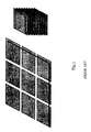
- Figure 1 illustrates a 2D- versus 3-D integration scheme and clearly shows that a large number of the long interconnects needed in 2-D structures could be replaced by short vertical interconnects and greatly enhance performance.
- stacking just two wafers should offer an increase in performance by 15%, decrease power by 30% and reduce cost by 15% simply due to the decreased path lengths and required layers of metal to connect the transistors.
- a first problem is related to the thermal budget available after etching the deep via through the BEOL, FEOL and subsequent silicon substrate.
- These deep vias are filled with conductive materials such as copper, a barrier layer such as TaN and optionally a copper seed layer.
- conductive materials such as copper, a barrier layer such as TaN and optionally a copper seed layer.
- barrier layer such as TaN
- copper seed layer optionally a copper seed layer.
- dielectric isolator liner
- these dielectric isolators e.g.
- TEOS oxide are deposited before the deposition of said conductive materials by means of thermal and plasma enhanced deposition techniques (such as LP-CVD, ALD, PE-CVD, etc.) which typically have a rather high thermal budget which is not compatible at that stage of the processing (thermal budget is preferably lower than 450°C).
- a second problem to the creation of said deep vias is related to hardmask selective (etch) processing, which is very difficult to achieve at that stage of the processing.
- etch hardmask selective
- a very thick hardmask layer needs to be deposited (to avoid damage to layers underneath) which leads to hardmask residues afterwards that need to be removed by e.g. Chemical Mechanical Polishing (CMP).
- CMP Chemical Mechanical Polishing
- Said CMP processing is very critical and difficult to perform at that stage of the processing, e.g. damage to the W contact plugs is absolutely to be avoided.
- via holes are created after full completion of FEOL and BEOL processing. These vias are first filled with an organic adhesive layer such that a handling wafer (also called carrier wafer) could be glued onto the top substrate. Subsequently the backside of the wafer is thinned as far as the via holes such that these vias are opened from the back and connected in subsequent processing to a second wafer surface. The carrier wafer and organic adhesive are then removed and the via is filled with conductive material such as tungsten.
- a handling wafer also called carrier wafer
- the present invention provides a method for fabricating a wafer (and its active IC devices), to be used in a three dimensional stacked semiconductor device.
- the present invention provides a method for fabricating a three dimensional stacked semiconductor device, comprising the steps of:
- a method according to the invention can further comprise, after said BEOL processing, the steps of:
- the step of forming said partially filled via can comprise the steps of:
- a method of the invention can further comprise the step of forming a separating layer in said via.
- Said separating layer can be a thermally grown silicon-dioxide layer.
- At least one additional isolation layer can be deposited within said via. More particularly, a combination of a silicon-nitride layer with a silicon-dioxide layer on top of said silicon-nitride layer or a Cu barrier layer with a silicon-dioxide layer on top of said barrier layer can be deposited in said via.
- said step of forming said spacers can comprises the steps of:
- said spacers material is silicon-dioxide.
- Said sacrificial material can be removed by an isotropic etching process.
- said sacrificial material is poly-silicon.
- Said sealing layer can be deposited by a conformal deposition process, such as a CVD process.
- Said sealing layer can further be planarized, e.g. by means of Chemical Mechanically Planarization.
- said first and/or second wafer substrate is silicon.
- said via has a diameter comprised between about 1 ⁇ m and about 10 ⁇ m, more preferably, comprised between about 2 ⁇ m and about 6 ⁇ m.
- said via has a depth in the wafer comprised between about 10 ⁇ m and about 100 ⁇ m, more preferably comprised between about 20 ⁇ m and about 50 ⁇ m.
- said contact hole(s) is/are created during Front End Of Line processing, e.g. by means of dry etching.
- said contact hole (s) can have a diameter comprised between 100nm and 200nm.
- a method according to the invention can further comprise the step of depositing a barrier layer onto the sidewalls of said contact hole(s).
- Said barrier layer can be a Ta(N), Ti(N), TaSiN, TiSiN, TiW, or W(C)N layer, or a Ru containing layer.
- said first conductive material is tungsten.
- said contact plug(s) in the airgap via is/are formed simultaneously with the contact plugs in the active devices of the semiconductor device.
- the step of making a contact to said contact plug(s) by performing conventional BEOL processing can be referred to as the connexion(s) made between different (at least two) metal structures in said first wafer.
- a method according to the invention can further comprise the step of depositing an etch stop layer and a dielectric layer (on top of said etch stop layer), after the creation of the airgap and airgap plug.
- Said etch stop layer can be a SiON, Si 3 N 4 , SiC or SiCN layer.
- said thinning step (for opening the airgap at the backside of the wafer) is performed by a combination of chemical and mechanical removal processes such as grinding, chemical mechanical polishing, etching, etc.
- a barrier layer is deposited if not already done before sealing said via. More particularly, a barrier layer can first be deposited and then a seed layer or catalyst nuclei can be deposited onto the sidewalls of said via (before sealing step) or of said opened airgap (after thinning step).
- said second conductive material can be deposited by conventional physical vapor deposition (PVD), chemical vapor deposition (CVD), electroless deposition, electroplating or (direct) plating.
- PVD physical vapor deposition
- CVD chemical vapor deposition
- electroless deposition electroplating or (direct) plating.
- Said second conductive material can be a metal (such as aluminum (Al) or tungsten (W)), a conductive polymer, a metal silicide and/or conductive carbon nanotubes (CNT) or conductive nanowires.
- a metal such as aluminum (Al) or tungsten (W)
- a conductive polymer such as aluminum (Al) or tungsten (W)
- a metal silicide and/or conductive carbon nanotubes (CNT) or conductive nanowires is copper.
- Another object of the invention is a semiconductor device obtainable by a method according to the invention.
- the intermediate structures (such as represented in figures 5F to 5H and figures 6A to 6E, more particularly such as represented in figure 5H and in figure 6E) obtainable by a method of the invention are also objects of the present invention.
- Said intermediate structures (which can also be referred to as intermediate semiconductor devices) can be used for the fabrication of three dimensional stacked semiconductor device.
- a three dimensional stacked semiconductor device comprises:
- Said conductive material in said through wafer via can be a metal (such as copper (Cu), aluminum (Al) or tungsten (W)), a conductive polymer, a metal silicide and/or conductive carbon nanotubes (CNT) or conductive nanowires.
- a metal such as copper (Cu), aluminum (Al) or tungsten (W)
- a conductive polymer such as copper (Cu), aluminum (Al) or tungsten (W)
- a conductive polymer such as copper (Cu), aluminum (Al) or tungsten (W)
- a conductive polymer such as copper (Cu), aluminum (Al) or tungsten (W)
- a conductive polymer such as copper (Cu), aluminum (Al) or tungsten (W)
- CNT conductive carbon nanotubes
- said conductive material in said through wafer via is copper.
- a three dimensional stacked semiconductor device can further comprise, along the sidewalls of said through wafer via, at least one isolation layer.
- Said at least one isolation layer can be a combination of a silicon-nitride layer with a silicon-dioxide layer on top of said silicon-nitride layer.
- it can be a combination of a Cu barrier layer with a silicon-dioxide layer on top of said barrier layer.
- said copper barrier layer can be made of Ta(N), Ti(N), TaSiN, TiSiN, TiW, or W(C)N, or of a Ru containing layer.
- a three dimensional stacked semiconductor device can further comprise, along the sidewalls of said through wafer via, a seedlayer or catalysts on top of said at least one isolation layer.
- a three dimensional stacked semiconductor device further comprises at least one contact plug within said through wafer via.
- said contact plug is made of W.
- Figure 1 illustrates a 2D- versus 3-D integration scheme and clearly shows that a large number of the long interconnects needed in 2-D structures could be replaced by a short vertical interconnect that greatly enhances performance.
- Figure 2 illustrates a 3-D integration scheme using a through wafer via that is created after BEOL processing.
- Figure 3 illustrates the 3-D integration scheme according to the current invention using a through wafer via that is created before FEOL processing comprising W plugs within the airgap plug and which is filled with conductive material after full completion of BEOL processing.
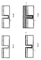
- Figures 4A to 4I illustrate the different processing steps for forming a deep via airgap using the method of a preferred embodiment.
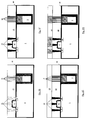
- Figures 5A to 5H illustrate the additional processing steps to create contact plugs within the airgap plug in case the deep via airgap is used to form through wafer vias or deep vias filled with conductive material using the method of a preferred embodiment.
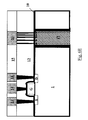
- Figures 6A to 6E illustrate the different processing steps for forming a through wafer via or deep via filled with conductive material.
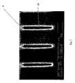
- Figure 7 shows a SEM picture illustrating the formation of a deep airgap 18 after removal of the sacrificial material (poly-silicon) by isotropic etching and deposition of a conformal layer 6 (e.g., TEOS-oxide deposition by Chemical Vapor deposition) to close the airgap.
- a conformal layer 6 e.g., TEOS-oxide deposition by Chemical Vapor deposition
- a method for forming a "deep via airgap" in a semiconductor substrate is disclosed.
- FEOL Front End of Line
- BEOL Back End Of Line
- said deep via airgap has a diameter from 1 ⁇ m up to 10 ⁇ m and more preferred between 2 and 6 ⁇ m.
- said deep via airgap has a depth into the substrate (also referred to as length) from 10 ⁇ m up to 100 ⁇ m and more preferred between 20 and 50 ⁇ m.
- a method of the invention for forming deep via airgaps comprises the step of first patterning a via (hole) in a substrate.
- Said substrate is preferably a semiconductor substrate such as a Si wafer.
- said step is performed before any semiconductor processing, e.g. before the creation of active components has taken place.
- a separating layer is formed on the sidewalls of said via. More particularly, an isolation liner can be thermally grown onto the sidewalls of said via, by exposing the sidewalls to an oxidizing ambient.
- said isolation liner is made of silicon-dioxide such as TetraEthylOrthoSilicate-oxide (TEOS-oxide) or a nitride such as Si 3 N 4 .
- TEOS-oxide TetraEthylOrthoSilicate-oxide
- Si 3 N 4 a nitride
- extra conformal layers can be deposited, such as combinations of a nitride layer with a silicon-dioxide layer on top of said nitride layer or a Cu barrier layer with a silicon-dioxide layer on top of said barrier layer.
- said via is partly or completely filled with a sacrificial material (e.g., polysilicon).
- a sacrificial material e.g., polysilicon
- the via is completely filled with sacrificial material
- techniques such as dry etch or wet etch can be used to remove said sacrificial material such that a partly filled via is created.
- spacers are formed on the sidewalls of the unfilled part of the via.
- said spacers are made of TEOS-oxide and said spacers are used to narrow the opening of the via.
- the remaining part of the sacrificial material e.g. by isotropic etching
- a sealing layer preferably a conformal layer of TEOS-oxide
- the sealing part of said deep via airgap is also referred to as the airgap plug.
- the method for forming a deep via airgap is preferably used to fabricate a through wafer or deep via filled with conductive material for wafer to wafer or die to die interconnect also referred to as three dimensional (3D) stacking of wafers or dies.
- contact plugs e.g. W plugs
- W plugs are created within the airgap plug to establish an interconnect with the lines (preferably copper lines) within the BEOL.
- Advantages of a method of the invention (according to a preferred embodiment) to fabricate through wafer or deep vias for wafer to wafer interconnect, starting from (using) an airgap via created before FEOL processing, are the fact that there is no thermal budget at that stage, there are no limitations in choice of hardmask layers to be used for patterning the via and there is no waste of valuable surface area in the BEOL level.
- a deep via airgap is preferably created before FEOL processing is started, and after completion of a full BEOL processing, said deep via airgap can be transformed into a through wafer or deep via filled with conductive material.
- Said isolation liner is deposited to isolate the deep via filled with conductive material (as described in further processing) towards the bulk Si substrate.
- a barrier layer can be deposited on the sidewalls of the deep via airgap.
- a method for transforming the deep via airgap of the current invention into a through wafer or deep via filled with conductive material is disclosed.
- Said transformation is performed after completion of a full FEOL and BEOL processing.
- the method starts with (comprises the step of) thinning the backside of the wafer such that the deep via airgap is opened.
- Said thinning of the wafer is preferably achieved by chemical mechanical polishing, grinding and/or silicon wet etch processes.
- part of the airgap plug is removed such that the contact plugs (e.g. W plugs) are free (i.e. the extremities are not embedded any longer within the sealing material) (at the bottom of) within the deep via airgap.
- the contact plugs e.g. W plugs
- a barrier layer needs to be formed onto the sidewalls of said deep via to avoid migration of conductive material into the substrate.
- a suitable conductive material is then deposited into the deep via.
- Said conductive material can be a metal (such as copper, aluminum, tungsten), a conductive polymer, metal silicides, conductive carbon nanotubes (CNT), and/or conductive nanowires, etc.
- Deposition processes such as conventional physical vapor deposition (PVD), chemical vapor deposition (CVD), electrochemical methods such as electroplating (ECP)/electrodeposition (ECD) and direct plating can be used to fill up said via and if necessary or optionally a seed layer can be deposited first. If the contact plugs can be used as starting point for electrochemical plating, there is no need to deposit a seedlayer first.
- a method according to the invention can be used to create a three dimensional stacked semiconductor device.
- Said device is also referred to as 3 dimensional Interconnect (IC) stacking, wafer to wafer bonding and wafer stacking.
- IC 3 dimensional Interconnect
- Said device is characterized as comprising at least a first wafer having a through wafer via filled with conductive material and a second wafer.
- said through wafer via is situated completely in the wafer substrate of the first wafer.
- Both wafers further comprise active IC devices (FEOL and BEOL interconnect structures).
- Said first wafer and second wafer are contacted to each other by means of the through wafer via, situated in the first wafer, and preferably the back side of the first wafer which comprises the through wafer via is connected (also referred to as bonding) to the front side of the second wafer.
- the through wafer via is connected to the interconnect structures situated in the second wafer.
- Three dimensional stacking of wafers include e.g. stacking of respectively logic and memory products, stacking of low power units with defect tolerant memory units and SOC (System On Chip) type products.
- a method for fabricating a vertical stack of at least two wafers to create a three dimensional stacked semiconductor device using a through wafer via is provided.
- a method according to the invention can comprise the steps of:
- the step of forming the partially filled-in portion of the hole can comprise the steps of:
- a method of the invention can further comprise the step of forming a separating layer in said hole.
- Said separating layer is preferably a thermally grown silicon-dioxide layer.
- a method of the invention can further comprise the deposition of at least one additional isolation layer within said via.
- Said isolation layer can be a combination of a silicon-nitride layer with a silicon-dioxide layer on top of said silicon-nitride layer or a Cu barrier layer with a silicon-dioxide layer on top of said barrier layer.
- the step of forming said spacers can comprise the steps of:
- said spacers material is silicon-dioxide.
- said sacrificial material can be removed by an isotropic etching process.
- said sacrificial material is poly-silicon.
- Said sealing layer can be deposited by a conformal deposition process, such as a CVD process.
- a method according to the invention can further comprise a step of planarizing said sealing layer.
- Said planarizing step can performed by means of Chemical Mechanically Planarization.
- said wafer is silicon wafer.
- said contact hole(s) is/are created during Front End Of Line processing (e.g. by means of dry etching).
- said contact plug(s) in the airgap via is/are simultaneously created with the contact plugs in the active devices of the semiconductor device.
- the contact holes have a diameter of 100nm up to 200nm.
- a method of the invention can further comprise the step of depositing an etch stop layer and a dielectric layer on top of said etch stop layer, after the creation of the airgap with airgap plug.
- said etch stop layer is a SiON, Si 3 N 4 , SiC or SiCN layer.
- a barrier layer can be deposited onto the sidewalls of said contact hole(s).
- Said barrier layer can be a Ta(N), Ti(N), TaSiN, TiSiN, TiW, or W(C)N layer, or a ruthenium (Ru) containing layer.
- the contact hole(s) is/are filled with a conductive material for contact plug(s), preferably tungsten.
- the thinning of the backside of the wafer can be performed by a combination of chemical and mechanical removal processes such as grinding, chemical mechanical polishing, etching, etc.
- a method of the invention can further comprise the deposition of first a barrier layer and second a seed layer or catalyst nuclei onto the sidewalls of the airgap via.
- the conductive material used to fill the airgap via can be deposited by conventional physical vapor deposition (PVD), chemical vapor deposition (CVD), electroless deposition (also referred to as electroplating) or (direct) plating.
- PVD physical vapor deposition
- CVD chemical vapor deposition
- electroless deposition also referred to as electroplating
- direct plating direct
- Another object of the present invention is a semiconductor device obtainable by a method according to the invention.
- a three dimensional stacked semiconductor device comprising:
- Said conductive material in said through wafer via can be a metal, a conductive polymer, a metal silicide and/or conductive carbon nanotubes (CNT) or conductive nanowires.
- said conductive material is copper (Cu), aluminum (Al) or tungsten (W).
- a three dimensional stacked semiconductor device of the invention preferably comprises at least one isolation layer against the sidewalls of said through wafer via.
- Said at least one isolation layer can be a combination of a silicon-nitride layer with a silicon-dioxide layer on top of said silicon-nitride layer or a Cu barrier layer with a silicon-dioxide layer on top of said barrier layer. More particularly, it can be a combination of a Cu barrier layer with a silicon-dioxide layer on top of said barrier layer, wherein said copper barrier layer is made of Ta(N), Ti(N), TaSiN, TiSiN, TiW, or W(C)N.
- a three dimensional stacked semiconductor device of the invention preferably further comprises along the sidewalls of said through wafer via, a seedlayer or catalysts, on top of said at least one isolation layer(s).
- said through wafer via has a diameter of about 1 ⁇ m up to about 10 ⁇ m, and more preferably of about 2 ⁇ m up to about 6 ⁇ m.
- said through wafer via has a depth in the wafer of about 10 ⁇ m up to about 100 ⁇ m, more preferably of about 20 ⁇ m up to about 50 ⁇ m.
- sacrificial is a broad term and is used without limitation, as a material or a layer that is deposited temporarily, and that is not supposed to remain, at least totally, in the final device, or a material or layer that is destined to be removed, at least partially, during the process of fabricating a device.
- spacer is a broad term and is used without limitation, as a material or layer that is deposited on the uncovered parts of the sidewalls of the via that is partially filled with a sacrificial material, in order to narrow the opening of said via.
- the step of forming spacers can include two sub-steps: deposition of a layer of a spacer material that closes or substantially narrows the opening, preferably by a conformal deposition process; and then etching back the layer of the spacer material, whereby the spacer is formed.
- the etchback step can be performed by any suitable etching process, preferably an anisotropic dry etch process (Reactive Ion Etch also referred to as RIE).
- wafer stacking preferably refers to vertical stacking of at least two wafers on top of each other, and using through-wafer (e.g. through-silicon) vias (interconnects) situated in a first wafer to connect to the interconnect structures of the second wafer.
- through-wafer e.g. through-silicon
- interconnects interconnects
- Said through-wafer (e.g. through-silicon) vias are filled with conductive material.
- Said wafers are preferably identically sized/shaped wafers but not limited to that.
- vertical stacked or vertical stacking of wafers preferably refers to stacking of at least two wafers whereby the backside of the first wafer is connected to the front-side of the second wafers by means of at least one through wafer (e.g. through-silicon) via situated in the first wafer and connecting interconnect structures of both wafers. This can be repeated several times.
- through wafer e.g. through-silicon
- the substrate 1 is a Si wafer.
- the substrate 1 is preferably a bare silicon wafer before any semiconductor processing such as FEOL processing.
- a "substrate protecting layer" 2 can be deposited.
- this protecting layer 2 and the substrate are patterned.
- a via needs to be patterned first.
- photosensitive layers need to be deposited and the via pattern is transferred into said photosensitive layers using photolithography.
- a hardmask layer is deposited onto the substrate first.
- Said hardmask layer can be used to transfer the photolithographic pattern using dry etch processing.
- the hardmask pattern is then transferred into the substrate using dry-etch processing.
- said deep via airgap has a diameter from 1 ⁇ m up to 10 ⁇ m and more preferred between 2 and 6 ⁇ m.
- the depth (into the substrate) of said deep via airgap is from 10 ⁇ m up to 100 ⁇ m and more preferred between 20 and 50 ⁇ m.
- the anisotropic patterning of the via is done by dry etch (e.g. a reactive ion plasma based etch).
- first a separating layer can be formed within the via.
- This layer can be employed when it is difficult to remove the sacrificial material 4 selectively towards the substrate 1 afterwards.
- an isolation liner is thermally grown onto the sidewalls by exposing the sidewalls to an oxidizing ambient, more specifically a 20 nm oxide layer as a separating layer is grown into the Si via surface (depicted in Figure 4B) by a thermal or wet oxidation process.
- At least one additional (preferably conformal) layer(s) 22, acting as isolation layer or barrier layer can be deposited onto the sidewalls of the via, such as combinations of a silicon-nitride layer with a silicon-dioxide layer on top of said silicon-nitride layer or a Cu barrier layer with a silicon-dioxide layer on top of said barrier layer.
- said isolation liner is made of silicon-dioxide such as TetraEthylOrthoSilicate-oxide (TEOS-oxide) or a silicon-nitride such as Si 3 N 4 .
- TEOS-oxide TetraEthylOrthoSilicate-oxide
- Si 3 N 4 silicon-nitride
- Said additional layers 22 as shown in Figure 4C can be of variable thicknesses (e.g. up to and including about 300nm in thickness).
- said layer can act as an isolation layer or in case the deep via airgap is used to create through wafer vias an extra liner acting as a barrier layer to prevent migration of conductive material towards the substrate can be deposited (optionally).
- the deposited material can be an oxide such as TEOS-oxide or Si 3 N 4 , however, any other suitable dielectric material can be alternatively employed.
- the sacrificial material 4 is deposited to fill the via (see Figure 4D).
- Any suitable sacrificial material can be employed. While polysilicon is generally preferred, other materials, for example, amorphous silicon, an oxide (removed by a wet etch) and appropriate organic materials having sufficient thermal budget can be used as alternative materials.
- CMP Chemical Mechanical Polishing
- etchback process wet or dry
- deposited liner 22 can act as a stopping layer.
- the sacrificial material 4 in the via is removed (e.g., by means of an etchback) until a level below the top of the protecting layer 2 is achieved such that a partly filled via is created (see Figure 4E). A portion of the sidewalls of said partly filled via is thus exposed and can be used to form spacers in a next step.
- spacers 5 are formed to narrow the opening of the via.
- the spacers are formed by a deposition process (e.g., a conformal deposition process) followed by an etchback process (e.g., an anisotropic etchback process).
- a deposition process e.g., a conformal deposition process
- an etchback process e.g., an anisotropic etchback process.
- an oxide spacer is formed, more specifically, TEOS-oxide spacers are formed.
- a liner can be deposited first, such as a (e.g. 10 nm) nitride liner.
- the nitride layer can facilitate end point detection.
- the distance between the spacers after spacer formation is as close as possible (i.e. the opening is as narrow as possible).
- the sacrificial material is removed through the opening formed, between the spacers (see Figure 4G).
- the sacrificial material is polysilicon and is preferably removed by, e.g. a SF 6 based isotropic dry etch plasma. Other reactive gases can also be employed. Likewise, techniques such as down stream etching can be suitably employed as well.
- the sacrificial material is converted into a gas that can leave through the opening between the spacers. If oxide is used as a protective layer, the etching is selective towards oxide.
- the opening between the spacers is sealed via a deposition process.
- a conformal oxide deposition process is employed to form the sealing layer 6 (e.g., a TEOS layer formed by Chemical Vapor Deposition).
- Figure 4H shows the deep via airgap 7 formed after sealing the opening, a negligible amount of sealing material may be deposited inside the via (not shown).
- the deposited sealing layer 6 can be further planarized (e.g., by chemical mechanical planarization), stopping at the protecting layer 2. Accordingly, a deep via airgap is created that is situated completely in the substrate. While the above-described procedure is generally preferred for sealing the airgap, other deposition processes can also be suitable for use. Likewise, a non-conformal deposition process can alternatively be employed.
- the deposition of the sacrificial material 4 can be such that a partly filled via is created and no further etchback is conducted.
- Figure 7 shows a SEM picture illustrating the formation of an airgap 18 after removal of the sacrificial material (polysilicon) by isotropic etching and deposition of a conformal layer 6 (e.g., TEOS-oxide deposition by Chemical Vapor deposition) to close the airgap.
- a conformal layer 6 e.g., TEOS-oxide deposition by Chemical Vapor deposition
- the methods of the preferred embodiments for forming deep via airgaps can be successfully applied to the formation of deep vias or through wafer vias to create 3D wafer interconnect structures.
- said deep vias have a depth of from about 10 ⁇ m to about 100 ⁇ m (most preferred between 20 ⁇ m and 50 ⁇ m).
- said deep vias have a diameter of about 1 ⁇ m to 10 ⁇ m (most preferred between 2 ⁇ m and 6 ⁇ m).
- one or more contact holes are created in the airgap plug 8.
- Said contact hole(s) is/are needed to establish electrical contact to the interconnect lines (preferably copper interconnect lines) of the BEOL structure created later on.
- said contact hole(s) has/have a diameter of about 100 to 200nm and most preferred about 150nm.
- the deep via is of a larger size also larger contact(s) can be considered.
- said contact hole(s) is/are created during conventional FEOL processing.
- More preferred said contact hole(s) is/are created simultaneously with the formation of plugs (preferably W plugs) in the active areas (comprising source, drain and gate) of the FEOL.
- a layer 10 is deposited onto the substrate comprising the airgap via and active areas.
- Said deposited layer 10 preferably has a thickness of around 50nm and is preferably made of SiON, Si 3 N 4 , SiC or SiCN but not limited thereto.
- the Pre Metal Dielectric (PMD) layer 13 is deposited.
- the pattern to create the contact holes 11 can be transferred into the PMD layer 13.
- Said pattern can be etched into the PMD layer 13 by an etch process selective towards said deposited layer 10 and using said deposited layer 10 as stopping layer as shown in Figures 5C and 5D.
- the deposited layer 10 at the bottom of said created contact holes 11 can be removed and the contact holes 11 in the airgap plug 8 can be slightly extended as shown in Figure 5E.
- a barrier layer such as TiN can be deposited first and subsequently said contact holes can be filled with a conductive material such that contact plugs 12 are created.
- said contact plugs are made of tungsten (W).
- the IMD (Inter-Metal-Dielectric) layer 15 can be deposited and within said IMD layer conductive structures 14 can be created to establish contact between the plugs 12 and BEOL interconnect structures of the BEOL.
- the wafer front side is preferably first deposited onto a carrier wafer.
- part of the airgap plug 8 is removed such that the contact plugs 12 (e.g. W plugs) are free (at least the extremities) (at the bottom of) in the deep via airgap.
- the contact plugs 12 e.g. W plugs
- a barrier layer 16 needs to be formed onto the sidewalls of said deep via 7 to avoid migration of conductive material into the substrate.
- any suitable conductive material is then deposited into the deep via.
- Said conductive material is preferably a metal such as copper (Cu), aluminum (Al) or tungsten (W), alternatively a conductive polymer, metal silicides and/or conductive carbon nanotubes (CNT) or conductive nanowires can be considered as conductive materials.
- Deposition processes such as conventional physical vapor deposition (PVD), chemical vapor deposition (CVD), electroless deposition, electroplating and (direct) plating can be used to fill up said via and if necessary or optionally a seed layer or catalyst (nuclei or layer) can be deposited first depending on the deposition technique. Said seedlayer will be different depending on the conductive material used to fill the via.
- Direct Plating can be used to deposit a seed layer (by using an alkaline bath with very low Cu concentration) in a first step and subsequently fill the via with conductive material (preferably copper) in a second electroplating step involving the use of a conventional acidic plating bath.
- conductive material preferably copper
- Electroplating has the advantage that it does not require an electrical contact. Electroless deposition is further characterized as a highly selective deposition technique which requires the use of catalyst nuclei that are deposited by galvanic displacement reactions on metals.
- barrier layers e.g. Ta/TaN, Ti/TiN, W-based barriers, etc.
- Pd can be used as a catalyst.
- planarization process e.g. Chemical Mechanical Planarization
- Figure 3 illustrates the deep via filled with conductive material in a 3D interconnect structure (here vertically stacking of two wafers is shown).
- the contact plugs 12 preferably W contact plugs
- active devices comprising source/gate/drain
Landscapes
- Element Separation (AREA)
- Internal Circuitry In Semiconductor Integrated Circuit Devices (AREA)
- Metal-Oxide And Bipolar Metal-Oxide Semiconductor Integrated Circuits (AREA)
Abstract
Description
- The present invention is related to the field of forming deep vias filled with a gas (air) in a semiconductor substrate, also referred to as deep via airgaps.
- Said deep via airgaps are used to create through wafer vias filled with conductive material for three dimensional (3D) wafer to wafer interconnect structures also referred to as vertically stacking of wafers or three dimensional semiconductor integrated circuit devices.
- For decades, semiconductor manufacturers have been shrinking transistor size in ICs to achieve the yearly increases in speed and performance described by Moore's Law - chip performance will double every ~18 months. Moore's Law exists only because the RC delay has been negligible in comparison with signal propagation delay. For submicron technology, however, RC delay becomes a dominant factor. It was hoped that change to copper metallurgy, low-k dielectrics and chemical mechanical polishing (CMP) would lower the RC delay and allow the performance increases predicted by device scaling and Moore's Law to continue through this decade.
- While copper and CMP have been integrated smoothly into the IC fabrication process, the same cannot be said for spin-on or CVD low-k dielectrics. To lower the permittivity and thus the line capacitance, IC manufacturers were forced to resort to materials with no prior history in chip production. The semiconductor industry has postponed three times (three nodes) the transition to true low-k (k<2.8) ILDs, with reliability and yield problems being the major suspects for the implementation delays.
- This inability to smoothly integrate low-k has generated many discussions concerning the end of device scaling as we know it, and has hastened the search for solutions beyond the perceived limits of current 2-D silicon devices. One emerging solution is 3-D integration also referred to as 3D interconnect. 3D interconnect structures are advantageously not only because of the size reduction, other drivers are mainly the fact that in 2D structures long interconnects are too slow and consume too much power. If a large number of these long interconnects needed in 2-D structures could be replaced by short vertical interconnects, this would greatly enhance performance. While silicon real estate is consumed by the vertical interconnect, a significant inter-wafer interconnect density can be achieved with a minimal area penalty. Figure 1 illustrates a 2D- versus 3-D integration scheme and clearly shows that a large number of the long interconnects needed in 2-D structures could be replaced by short vertical interconnects and greatly enhance performance. In particular, stacking just two wafers should offer an increase in performance by 15%, decrease power by 30% and reduce cost by 15% simply due to the decreased path lengths and required layers of metal to connect the transistors.
- In prior art several solutions are described to realize a 3D stacking of wafers in which the direct wafer to wafer (or die to die) stacking with vertical connections through the silicon are realized by means of "through wafer" vias filled with copper. These through wafer vias are etched after completion of the full Front End of Line (FEOL) processing and often after complete BEOL processing. A modified damascene technique is used to fill said through wafer vias with conductive material such as copper.
- In the realization of these "through wafer" vias or deep vias there are still a lot of problems to be solved. A first problem is related to the thermal budget available after etching the deep via through the BEOL, FEOL and subsequent silicon substrate. These deep vias are filled with conductive materials such as copper, a barrier layer such as TaN and optionally a copper seed layer. To isolate said conductive materials from the bulk of the substrate there is a need to deposit a dielectric isolator (liner) within the via. Typically, these dielectric isolators (e.g. TEOS oxide) are deposited before the deposition of said conductive materials by means of thermal and plasma enhanced deposition techniques (such as LP-CVD, ALD, PE-CVD, etc.) which typically have a rather high thermal budget which is not compatible at that stage of the processing (thermal budget is preferably lower than 450°C).
- A second problem to the creation of said deep vias is related to hardmask selective (etch) processing, which is very difficult to achieve at that stage of the processing. A very thick hardmask layer needs to be deposited (to avoid damage to layers underneath) which leads to hardmask residues afterwards that need to be removed by e.g. Chemical Mechanical Polishing (CMP). Said CMP processing is very critical and difficult to perform at that stage of the processing, e.g. damage to the W contact plugs is absolutely to be avoided.
- In US 6,448,174 via holes are created after full completion of FEOL and BEOL processing. These vias are first filled with an organic adhesive layer such that a handling wafer (also called carrier wafer) could be glued onto the top substrate. Subsequently the backside of the wafer is thinned as far as the via holes such that these vias are opened from the back and connected in subsequent processing to a second wafer surface. The carrier wafer and organic adhesive are then removed and the via is filled with conductive material such as tungsten.
- In US 6,645,832 first two wafers containing active IC devices (after finishing a full FEOL and BEOL processing) are bonded together via a metal bonding layer deposited on opposing (top) surfaces of both wafers at designated bonding areas such that electrical connections between active devices on both wafers are established. After the wafer bonding is completed one or more interwafer vias are etched in the top wafer top establish electrical connections of the active devices of both wafers and an external interconnect.
- The present invention provides a method for fabricating a wafer (and its active IC devices), to be used in a three dimensional stacked semiconductor device.
- More particularly, the present invention provides a method for fabricating a three dimensional stacked semiconductor device, comprising the steps of:
- patterning at least one via (or a hole) having sidewalls in a first wafer substrate,
- forming a via partially filled with sacrificial material, whereby a portion of the sidewalls of the via is exposed,
- forming spacers on said exposed portion of the sidewalls, whereby the via opening is narrowed,
- removing the sacrificial material through said narrowed opening;
- sealing said opening by depositing a sealing layer above the spacers such that an airgap is formed within said first wafer substrate, sealed by an airgap plug,
- creating at least one contact hole in said airgap plug and filling said contact hole(s) with a first conductive material such that at least one contact plug is created,
- depositing a conductive structure onto said contact plug(s),
- making a contact to said contact plug(s) by performing conventional BEOL processing.
- A method according to the invention can further comprise, after said BEOL processing, the steps of:
- thinning the backside (i.e. the wafer-substrate side) of the first wafer such that the airgap is opened,
- depositing a second conductive material in said opened airgap to create, in said first wafer, a through wafer via or a deep via filled with conductive material,
- contacting the backside of the first wafer by means of said through wafer via filled with said second conductive material to the interconnect structure situated in the frontside (i.e. the processed-side) of the second wafer.
- In a method according to the invention, the step of forming said partially filled via can comprise the steps of:
- completely filling said via with a sacrificial material, and
- etching back a portion of said sacrificial material, whereby a portion of the sidewalls is exposed.
- A method of the invention can further comprise the step of forming a separating layer in said via. Said separating layer can be a thermally grown silicon-dioxide layer.
- At least one additional isolation layer can be deposited within said via. More particularly, a combination of a silicon-nitride layer with a silicon-dioxide layer on top of said silicon-nitride layer or a Cu barrier layer with a silicon-dioxide layer on top of said barrier layer can be deposited in said via.
- In a method of the invention, said step of forming said spacers can comprises the steps of:
- optionally depositing a dry etch endpoint triggering layer, such as a nitride layer, then
- closing or narrowing the opening by depositing a layer (preferably a conformal layer) made of spacer material upon said via, and
- anisotropically etching back said spacers material allowing spacers formation.
- Preferably, said spacers material is silicon-dioxide.
- Said sacrificial material can be removed by an isotropic etching process. Preferably, said sacrificial material is poly-silicon.
- Said sealing layer can be deposited by a conformal deposition process, such as a CVD process.
- Said sealing layer can further be planarized, e.g. by means of Chemical Mechanically Planarization.
- Preferably, in a method of the invention, said first and/or second wafer substrate is silicon.
- Preferably, in a method according to the invention, said via has a diameter comprised between about 1 µm and about 10 µm, more preferably, comprised between about 2 µm and about 6 µm.
- Preferably, in a method according to the invention, said via has a depth in the wafer comprised between about 10 µm and about 100 µm, more preferably comprised between about 20 µm and about 50 µm.
- Preferably, in a method according to the invention, said contact hole(s) is/are created during Front End Of Line processing, e.g. by means of dry etching.
- For example, said contact hole (s) can have a diameter comprised between 100nm and 200nm.
- A method according to the invention can further comprise the step of depositing a barrier layer onto the sidewalls of said contact hole(s). Said barrier layer can be a Ta(N), Ti(N), TaSiN, TiSiN, TiW, or W(C)N layer, or a Ru containing layer.
- Preferably, in a method according to the invention, said first conductive material (in said contact hole(s)) is tungsten.
- Preferably, in a method according to the invention, said contact plug(s) in the airgap via is/are formed simultaneously with the contact plugs in the active devices of the semiconductor device.
- In a method of the invention, the step of making a contact to said contact plug(s) by performing conventional BEOL processing can be referred to as the connexion(s) made between different (at least two) metal structures in said first wafer.
- A method according to the invention can further comprise the step of depositing an etch stop layer and a dielectric layer (on top of said etch stop layer), after the creation of the airgap and airgap plug.
- Said etch stop layer can be a SiON, Si3N4, SiC or SiCN layer.
- Preferably, in a method according to the invention, said thinning step (for opening the airgap at the backside of the wafer) is performed by a combination of chemical and mechanical removal processes such as grinding, chemical mechanical polishing, etching, etc.
- In a method according to the invention, after said thinning step, a barrier layer is deposited if not already done before sealing said via. More particularly, a barrier layer can first be deposited and then a seed layer or catalyst nuclei can be deposited onto the sidewalls of said via (before sealing step) or of said opened airgap (after thinning step).
- In a method according to the invention, said second conductive material can be deposited by conventional physical vapor deposition (PVD), chemical vapor deposition (CVD), electroless deposition, electroplating or (direct) plating.
- Said second conductive material can be a metal (such as aluminum (Al) or tungsten (W)), a conductive polymer, a metal silicide and/or conductive carbon nanotubes (CNT) or conductive nanowires. Preferably said second conductive material, used to fill the opened airgap, is copper.
- Another object of the invention is a semiconductor device obtainable by a method according to the invention.
- In particular, the intermediate structures (such as represented in figures 5F to 5H and figures 6A to 6E, more particularly such as represented in figure 5H and in figure 6E) obtainable by a method of the invention are also objects of the present invention. Said intermediate structures (which can also be referred to as intermediate semiconductor devices) can be used for the fabrication of three dimensional stacked semiconductor device.
- A three dimensional stacked semiconductor device according to the invention comprises:
- a first wafer comprising active IC devices,
- a second wafer comprising active IC devices, and
- at least one through wafer via filled with conductive material, said through wafer via having a top, a bottom and sidewalls situated in the wafer substrate of said first wafer, for making the contact between said active devices of said first wafer and those of said second wafer.
- Said conductive material in said through wafer via can be a metal (such as copper (Cu), aluminum (Al) or tungsten (W)), a conductive polymer, a metal silicide and/or conductive carbon nanotubes (CNT) or conductive nanowires. Preferably, said conductive material in said through wafer via is copper.
- A three dimensional stacked semiconductor device according of the invention can further comprise, along the sidewalls of said through wafer via, at least one isolation layer. Said at least one isolation layer can be a combination of a silicon-nitride layer with a silicon-dioxide layer on top of said silicon-nitride layer. Or it can be a combination of a Cu barrier layer with a silicon-dioxide layer on top of said barrier layer. More particularly, said copper barrier layer can be made of Ta(N), Ti(N), TaSiN, TiSiN, TiW, or W(C)N, or of a Ru containing layer.
- A three dimensional stacked semiconductor device according to the invention can further comprise, along the sidewalls of said through wafer via, a seedlayer or catalysts on top of said at least one isolation layer.
- Preferably, a three dimensional stacked semiconductor device according to the invention further comprises at least one contact plug within said through wafer via. Preferably, said contact plug is made of W.
- All drawings are intended to illustrate some aspects and embodiments. Devices are depicted in a simplified way for reason of clarity. Not all alternatives and options are shown and therefore the preferred embodiments are not limited to the content of the given drawings. Like numerals are employed to reference like parts in the different figures.
- Figure 1 (PRIOR ART) illustrates a 2D- versus 3-D integration scheme and clearly shows that a large number of the long interconnects needed in 2-D structures could be replaced by a short vertical interconnect that greatly enhances performance.
- Figure 2 (PRIOR ART) illustrates a 3-D integration scheme using a through wafer via that is created after BEOL processing.
- Figure 3 illustrates the 3-D integration scheme according to the current invention using a through wafer via that is created before FEOL processing comprising W plugs within the airgap plug and which is filled with conductive material after full completion of BEOL processing.
- Figures 4A to 4I illustrate the different processing steps for forming a deep via airgap using the method of a preferred embodiment.
- Figures 5A to 5H illustrate the additional processing steps to create contact plugs within the airgap plug in case the deep via airgap is used to form through wafer vias or deep vias filled with conductive material using the method of a preferred embodiment.
- Figures 6A to 6E illustrate the different processing steps for forming a through wafer via or deep via filled with conductive material.
- Figure 7 shows a SEM picture illustrating the formation of a
deep airgap 18 after removal of the sacrificial material (poly-silicon) by isotropic etching and deposition of a conformal layer 6 (e.g., TEOS-oxide deposition by Chemical Vapor deposition) to close the airgap. - A method for forming a "deep via airgap" in a semiconductor substrate is disclosed.
- More specifically said deep via airgap is created before semiconductor processing such as Front End of Line (FEOL) and Back End Of Line (BEOL) processing in a semiconductor substrate such as a Si wafer.
- Preferably said deep via airgap has a diameter from 1µm up to 10µm and more preferred between 2 and 6 µm.
- Preferably said deep via airgap has a depth into the substrate (also referred to as length) from 10µm up to 100µm and more preferred between 20 and 50 µm.
- A method of the invention for forming deep via airgaps comprises the step of first patterning a via (hole) in a substrate.
- Said substrate is preferably a semiconductor substrate such as a Si wafer.
- Preferably, said step is performed before any semiconductor processing, e.g. before the creation of active components has taken place.
- Preferably, a separating layer is formed on the sidewalls of said via. More particularly, an isolation liner can be thermally grown onto the sidewalls of said via, by exposing the sidewalls to an oxidizing ambient.
- Preferably, said isolation liner is made of silicon-dioxide such as TetraEthylOrthoSilicate-oxide (TEOS-oxide) or a nitride such as Si3N4.
- Optionally, and depending on further applications of the deep via airgap, extra conformal layers can be deposited, such as combinations of a nitride layer with a silicon-dioxide layer on top of said nitride layer or a Cu barrier layer with a silicon-dioxide layer on top of said barrier layer.
- Subsequently, said via is partly or completely filled with a sacrificial material (e.g., polysilicon).
- In case the via is completely filled with sacrificial material, techniques such as dry etch or wet etch can be used to remove said sacrificial material such that a partly filled via is created.
- Within said partly filled via, spacers are formed on the sidewalls of the unfilled part of the via.
- Preferably said spacers are made of TEOS-oxide and said spacers are used to narrow the opening of the via.
- Through said narrowed opening, the remaining part of the sacrificial material (e.g. by isotropic etching) is preferably removed and the opening of the via is sealed by depositing a sealing layer (preferably a conformal layer of TEOS-oxide) above the spacers such that a "deep via airgap" is created.
- The sealing part of said deep via airgap is also referred to as the airgap plug.
- The method for forming a deep via airgap is preferably used to fabricate a through wafer or deep via filled with conductive material for wafer to wafer or die to die interconnect also referred to as three dimensional (3D) stacking of wafers or dies.
- In such applications, contact plugs (e.g. W plugs) are created within the airgap plug to establish an interconnect with the lines (preferably copper lines) within the BEOL.
- Advantages of a method of the invention (according to a preferred embodiment) to fabricate through wafer or deep vias for wafer to wafer interconnect, starting from (using) an airgap via created before FEOL processing, are the fact that there is no thermal budget at that stage, there are no limitations in choice of hardmask layers to be used for patterning the via and there is no waste of valuable surface area in the BEOL level.
- Said advantages result from a method of the invention wherein first a deep via airgap is preferably created before FEOL processing is started, and after completion of a full BEOL processing, said deep via airgap can be transformed into a through wafer or deep via filled with conductive material.
- During the creation of the deep via before FEOL processing, there is no limitation in thermal budget and a wide variety of conformal and better quality isolation liners such as LP-CVD-TEOS or Si3N4, which are typically deposited at higher temperatures, can be deposited onto the sidewalls of said deep via.
- Said isolation liner is deposited to isolate the deep via filled with conductive material (as described in further processing) towards the bulk Si substrate.
- Optionally, a barrier layer can be deposited on the sidewalls of the deep via airgap.
- Accordingly, in a first aspect, a method for transforming the deep via airgap of the current invention into a through wafer or deep via filled with conductive material is disclosed.
- Said transformation is performed after completion of a full FEOL and BEOL processing.
- Preferably the method starts with (comprises the step of) thinning the backside of the wafer such that the deep via airgap is opened.
- Said thinning of the wafer is preferably achieved by chemical mechanical polishing, grinding and/or silicon wet etch processes.
- Subsequently, part of the airgap plug is removed such that the contact plugs (e.g. W plugs) are free (i.e. the extremities are not embedded any longer within the sealing material) (at the bottom of) within the deep via airgap.
- If no barrier layer is deposited yet, a barrier layer needs to be formed onto the sidewalls of said deep via to avoid migration of conductive material into the substrate.
- A suitable conductive material is then deposited into the deep via. Said conductive material can be a metal (such as copper, aluminum, tungsten), a conductive polymer, metal silicides, conductive carbon nanotubes (CNT), and/or conductive nanowires, etc.
- Deposition processes such as conventional physical vapor deposition (PVD), chemical vapor deposition (CVD), electrochemical methods such as electroplating (ECP)/electrodeposition (ECD) and direct plating can be used to fill up said via and if necessary or optionally a seed layer can be deposited first. If the contact plugs can be used as starting point for electrochemical plating, there is no need to deposit a seedlayer first.
- A method according to the invention can be used to create a three dimensional stacked semiconductor device.
- Said device is also referred to as 3 dimensional Interconnect (IC) stacking, wafer to wafer bonding and wafer stacking.
- Said device is characterized as comprising at least a first wafer having a through wafer via filled with conductive material and a second wafer.
- In a device according to the invention, said through wafer via is situated completely in the wafer substrate of the first wafer.
- Both wafers further comprise active IC devices (FEOL and BEOL interconnect structures).
- Said first wafer and second wafer are contacted to each other by means of the through wafer via, situated in the first wafer, and preferably the back side of the first wafer which comprises the through wafer via is connected (also referred to as bonding) to the front side of the second wafer.
- More particularly, the through wafer via is connected to the interconnect structures situated in the second wafer.
- Applications including three dimensional stacking of wafers (dies) include e.g. stacking of respectively logic and memory products, stacking of low power units with defect tolerant memory units and SOC (System On Chip) type products.
- More particularly, a method for fabricating a vertical stack of at least two wafers to create a three dimensional stacked semiconductor device using a through wafer via is provided.
- A method according to the invention can comprise the steps of:
- patterning at least one via (or hole) having sidewalls in a first wafer substrate,
- forming a partially filled-in portion of the via, wherein the partially filled-in portion comprises a sacrificial material, whereby a portion of the sidewalls is exposed and a portion of the sidewalls is covered by the sacrificial material,
- forming spacers on the exposed portion of the sidewalls, whereby an opening to the via is narrowed,
- removing the sacrificial material through the narrowed opening,
- sealing the opening by depositing a layer above the spacers, whereby an airgap with airgap plug is formed,
- creating at least one contact hole in said airgap plug and filling said contact hole(s) with conductive material such that contact plug(s) is/are created,
- depositing a conductive structure onto the contact plug(s),
- performing conventional BEOL processing making contact to said contact plug(s),
- thinning the backside of the first wafer such that the airgap is opened,
- depositing conductive material in said deep via to create a through wafer via or deep via filled with conductive material in said first wafer,
- contacting the backside of the first wafer by means of said through wafer via filled with conductive material to the interconnect structure situated in the front-side of the second wafer.
- In a method of the invention, the step of forming the partially filled-in portion of the hole can comprise the steps of:
- completely filling the hole with a sacrificial material; and
- etching back a portion of the sacrificial material, whereby a portion of the sidewalls is exposed and a portion of the sidewalls is not (covered by the sacrificial material).
- A method of the invention can further comprise the step of forming a separating layer in said hole. Said separating layer is preferably a thermally grown silicon-dioxide layer.
- A method of the invention can further comprise the deposition of at least one additional isolation layer within said via. Said isolation layer can be a combination of a silicon-nitride layer with a silicon-dioxide layer on top of said silicon-nitride layer or a Cu barrier layer with a silicon-dioxide layer on top of said barrier layer.
- In a method of the invention, the step of forming said spacers can comprise the steps of:
- optionally depositing a dry etch endpoint triggering layer (such as a nitride layer), then
- closing or narrowing the opening by depositing a conformal layer made of spacer material upon said via (hole), and
- anisotropically etching back said spacers material allowing spacers formation.
- Preferably; said spacers material is silicon-dioxide.
- In a method of the invention, said sacrificial material can be removed by an isotropic etching process. Preferably said sacrificial material is poly-silicon.
- Said sealing layer can be deposited by a conformal deposition process, such as a CVD process.
- A method according to the invention can further comprise a step of planarizing said sealing layer. Said planarizing step can performed by means of Chemical Mechanically Planarization.
- Preferably, said wafer is silicon wafer.
- Preferably, in a method of the invention, said contact hole(s) is/are created during Front End Of Line processing (e.g. by means of dry etching).
- Preferably, said contact plug(s) in the airgap via is/are simultaneously created with the contact plugs in the active devices of the semiconductor device.
- Preferably, the contact holes have a diameter of 100nm up to 200nm.
- A method of the invention can further comprise the step of depositing an etch stop layer and a dielectric layer on top of said etch stop layer, after the creation of the airgap with airgap plug. Preferably, said etch stop layer is a SiON, Si3N4, SiC or SiCN layer.
- After the creation of said contact hole(s) a barrier layer can be deposited onto the sidewalls of said contact hole(s). Said barrier layer can be a Ta(N), Ti(N), TaSiN, TiSiN, TiW, or W(C)N layer, or a ruthenium (Ru) containing layer.
- After depositing preferably a conformal barrier layer into said contact hole(s), the contact hole(s) is/are filled with a conductive material for contact plug(s), preferably tungsten.
- In a method of the invention, the thinning of the backside of the wafer can be performed by a combination of chemical and mechanical removal processes such as grinding, chemical mechanical polishing, etching, etc.
- A method of the invention can further comprise the deposition of first a barrier layer and second a seed layer or catalyst nuclei onto the sidewalls of the airgap via.
- In a method of the invention, the conductive material used to fill the airgap via (preferably copper), can be deposited by conventional physical vapor deposition (PVD), chemical vapor deposition (CVD), electroless deposition (also referred to as electroplating) or (direct) plating.
- Another object of the present invention is a semiconductor device obtainable by a method according to the invention.
- More particularly, a three dimensional stacked semiconductor device is provided, comprising:
- a first wafer comprising active IC devices and having at least one through wafer via filled with conductive material, said through wafer via having a top, a bottom and sidewalls situated in the wafer substrate,
- a second wafer comprising active IC devices,
- said active devices of the first and second wafer making contact to each other by means of the through wafer.
- Said conductive material in said through wafer via can be a metal, a conductive polymer, a metal silicide and/or conductive carbon nanotubes (CNT) or conductive nanowires. Preferably, said conductive material is copper (Cu), aluminum (Al) or tungsten (W).
- A three dimensional stacked semiconductor device of the invention preferably comprises at least one isolation layer against the sidewalls of said through wafer via.
- Said at least one isolation layer can be a combination of a silicon-nitride layer with a silicon-dioxide layer on top of said silicon-nitride layer or a Cu barrier layer with a silicon-dioxide layer on top of said barrier layer. More particularly, it can be a combination of a Cu barrier layer with a silicon-dioxide layer on top of said barrier layer, wherein said copper barrier layer is made of Ta(N), Ti(N), TaSiN, TiSiN, TiW, or W(C)N.
- A three dimensional stacked semiconductor device of the invention preferably further comprises along the sidewalls of said through wafer via, a seedlayer or catalysts, on top of said at least one isolation layer(s).
- Preferably, said through wafer via has a diameter of about 1 µm up to about 10 µm, and more preferably of about 2 µm up to about 6 µm.
- Preferably, said through wafer via has a depth in the wafer of about 10 µm up to about 100 µm, more preferably of about 20 µm up to about 50 µm.
- The following description and examples illustrate a preferred embodiment of the present invention in detail. Those of skill in the art will recognize that there are numerous variations and modifications of this invention that are encompassed by its scope. Accordingly, the description of a preferred embodiment should not be deemed to limit the scope of the present invention.
- The term "sacrificial," as used herein, is a broad term and is used without limitation, as a material or a layer that is deposited temporarily, and that is not supposed to remain, at least totally, in the final device, or a material or layer that is destined to be removed, at least partially, during the process of fabricating a device.
- The term "spacer," as used herein, is a broad term and is used without limitation, as a material or layer that is deposited on the uncovered parts of the sidewalls of the via that is partially filled with a sacrificial material, in order to narrow the opening of said via. The step of forming spacers can include two sub-steps: deposition of a layer of a spacer material that closes or substantially narrows the opening, preferably by a conformal deposition process; and then etching back the layer of the spacer material, whereby the spacer is formed. The etchback step can be performed by any suitable etching process, preferably an anisotropic dry etch process (Reactive Ion Etch also referred to as RIE).
- The term "wafer stacking" preferably refers to vertical stacking of at least two wafers on top of each other, and using through-wafer (e.g. through-silicon) vias (interconnects) situated in a first wafer to connect to the interconnect structures of the second wafer. Said through-wafer (e.g. through-silicon) vias are filled with conductive material. Said wafers are preferably identically sized/shaped wafers but not limited to that.
- The term "vertically" stacked or vertical stacking of wafers preferably refers to stacking of at least two wafers whereby the backside of the first wafer is connected to the front-side of the second wafers by means of at least one through wafer (e.g. through-silicon) via situated in the first wafer and connecting interconnect structures of both wafers. This can be repeated several times.
- A general method for forming the deep via airgap is described hereafter. The method is schematically presented in Figures 4A to 4H.
- In the example depicted in the Figures, the
substrate 1 is a Si wafer. Thesubstrate 1 is preferably a bare silicon wafer before any semiconductor processing such as FEOL processing. - If the
substrate 1 is to be protected, a "substrate protecting layer" 2 can be deposited. - Subsequently, this
protecting layer 2 and the substrate are patterned. - To create a deep via airgap, a via needs to be patterned first. To perform said patterning, photosensitive layers need to be deposited and the via pattern is transferred into said photosensitive layers using photolithography.
- Optionally and also preferred a hardmask layer is deposited onto the substrate first. Said hardmask layer can be used to transfer the photolithographic pattern using dry etch processing.
- At this stage of the processing there is no limiting thermal budget such that a wide variety of hardmask layers are suitable. The hardmask pattern is then transferred into the substrate using dry-etch processing.
- Preferably said deep via airgap has a diameter from 1µm up to 10µm and more preferred between 2 and 6 µm.
- Preferably the depth (into the substrate) of said deep via airgap is from 10µm up to 100µm and more preferred between 20 and 50 µm.
- In the example shown in Figures 4A to 4H, the anisotropic patterning of the via is done by dry etch (e.g. a reactive ion plasma based etch).
- As shown in Figures 4B and 4C, first a separating layer can be formed within the via. This layer can be employed when it is difficult to remove the
sacrificial material 4 selectively towards thesubstrate 1 afterwards. In the example depicted in the Figures within said via first an isolation liner is thermally grown onto the sidewalls by exposing the sidewalls to an oxidizing ambient, more specifically a 20 nm oxide layer as a separating layer is grown into the Si via surface (depicted in Figure 4B) by a thermal or wet oxidation process. - Optionally, and depending on further applications of the deep via airgap, at least one additional (preferably conformal) layer(s) 22, acting as isolation layer or barrier layer, can be deposited onto the sidewalls of the via, such as combinations of a silicon-nitride layer with a silicon-dioxide layer on top of said silicon-nitride layer or a Cu barrier layer with a silicon-dioxide layer on top of said barrier layer.
- Preferably said isolation liner is made of silicon-dioxide such as TetraEthylOrthoSilicate-oxide (TEOS-oxide) or a silicon-nitride such as Si3N4.
- Said
additional layers 22 as shown in Figure 4C can be of variable thicknesses (e.g. up to and including about 300nm in thickness). Depending on the material of saidadditional layer 22, said layer can act as an isolation layer or in case the deep via airgap is used to create through wafer vias an extra liner acting as a barrier layer to prevent migration of conductive material towards the substrate can be deposited (optionally). In case the additional layer acts as an isolation layer, the deposited material can be an oxide such as TEOS-oxide or Si3N4, however, any other suitable dielectric material can be alternatively employed. - Subsequently, the
sacrificial material 4 is deposited to fill the via (see Figure 4D). Any suitable sacrificial material can be employed. While polysilicon is generally preferred, other materials, for example, amorphous silicon, an oxide (removed by a wet etch) and appropriate organic materials having sufficient thermal budget can be used as alternative materials. - Chemical Mechanical Polishing (CMP) or alternatively an etchback process (wet or dry) can be used to planarize this material towards the deposited
liner 22. In case Chemical Mechanical Polishing (CMP) is used as planarizing method, depositedliner 22 can act as a stopping layer. - The
sacrificial material 4 in the via is removed (e.g., by means of an etchback) until a level below the top of theprotecting layer 2 is achieved such that a partly filled via is created (see Figure 4E). A portion of the sidewalls of said partly filled via is thus exposed and can be used to form spacers in a next step. - In Figure 4F,
spacers 5 are formed to narrow the opening of the via. The spacers are formed by a deposition process (e.g., a conformal deposition process) followed by an etchback process (e.g., an anisotropic etchback process). In the example depicted in the Figures, an oxide spacer is formed, more specifically, TEOS-oxide spacers are formed. - For ease of dry etch endpoint triggering, a liner can be deposited first, such as a (e.g. 10 nm) nitride liner. The nitride layer can facilitate end point detection.
- In the example depicted in the Figures, the distance between the spacers after spacer formation is as close as possible (i.e. the opening is as narrow as possible).
- After spacer etching, the sacrificial material is removed through the opening formed, between the spacers (see Figure 4G). In the example depicted in the Figures, the sacrificial material is polysilicon and is preferably removed by, e.g. a SF6 based isotropic dry etch plasma. Other reactive gases can also be employed. Likewise, techniques such as down stream etching can be suitably employed as well. The sacrificial material is converted into a gas that can leave through the opening between the spacers. If oxide is used as a protective layer, the etching is selective towards oxide.
- Finally, the opening between the spacers is sealed via a deposition process. In the example depicted in the Figures, a conformal oxide deposition process is employed to form the sealing layer 6 (e.g., a TEOS layer formed by Chemical Vapor Deposition). Figure 4H shows the deep via
airgap 7 formed after sealing the opening, a negligible amount of sealing material may be deposited inside the via (not shown). The depositedsealing layer 6 can be further planarized (e.g., by chemical mechanical planarization), stopping at theprotecting layer 2. Accordingly, a deep via airgap is created that is situated completely in the substrate. While the above-described procedure is generally preferred for sealing the airgap, other deposition processes can also be suitable for use. Likewise, a non-conformal deposition process can alternatively be employed. - Alternatively, in a method according to the invention, the deposition of the
sacrificial material 4 can be such that a partly filled via is created and no further etchback is conducted. - Figure 7 shows a SEM picture illustrating the formation of an
airgap 18 after removal of the sacrificial material (polysilicon) by isotropic etching and deposition of a conformal layer 6 (e.g., TEOS-oxide deposition by Chemical Vapor deposition) to close the airgap. - The methods of the preferred embodiments for forming deep via airgaps can be successfully applied to the formation of deep vias or through wafer vias to create 3D wafer interconnect structures.
- In a device of the invention, said deep vias have a depth of from about 10 µm to about 100µm (most preferred between 20µm and 50µm). Preferably, said deep vias have a diameter of about 1µm to 10µm (most preferred between 2µm and 6µm).
- The additional processing steps needed to create deep vias or through wafer vias starting from airgap vias are illustrated in Figures 5A to 5H.
- After the creation of the airgap via as described in the present invention, one or more contact holes are created in the airgap plug 8.
- Said contact hole(s) is/are needed to establish electrical contact to the interconnect lines (preferably copper interconnect lines) of the BEOL structure created later on.
- Preferably said contact hole(s) has/have a diameter of about 100 to 200nm and most preferred about 150nm. However, since the deep via is of a larger size also larger contact(s) can be considered.
- Preferably said contact hole(s) is/are created during conventional FEOL processing.
- More preferred said contact hole(s) is/are created simultaneously with the formation of plugs (preferably W plugs) in the active areas (comprising source, drain and gate) of the FEOL.
- First, a
layer 10 is deposited onto the substrate comprising the airgap via and active areas. Said depositedlayer 10 preferably has a thickness of around 50nm and is preferably made of SiON, Si3N4, SiC or SiCN but not limited thereto. - Above the deposited
layer 10, the Pre Metal Dielectric (PMD)layer 13 is deposited. - By means of dry etch processing, the pattern to create the contact holes 11 can be transferred into the
PMD layer 13. Said pattern can be etched into thePMD layer 13 by an etch process selective towards said depositedlayer 10 and using said depositedlayer 10 as stopping layer as shown in Figures 5C and 5D. - Subsequently, the deposited
layer 10 at the bottom of said created contact holes 11 can be removed and the contact holes 11 in the airgap plug 8 can be slightly extended as shown in Figure 5E. - In said contact holes, a barrier layer such as TiN can be deposited first and subsequently said contact holes can be filled with a conductive material such that contact plugs 12 are created.
- Preferably said contact plugs are made of tungsten (W).
- Subsequently the IMD (Inter-Metal-Dielectric)
layer 15 can be deposited and within said IMD layerconductive structures 14 can be created to establish contact between theplugs 12 and BEOL interconnect structures of the BEOL. - Additional layers needed to transfer the pattern of the conductive structures need to be deposited first.
- The final deep via airgap comprising the contact plugs 12 and a conductive structure 14 (preferably made of copper) deposited onto the contact plugs 12 such that contact to interconnect lines of the BEOL can be established is shown in Figure 5H.
- The different processing steps to create the through wafer or deep via filled with conductive material are shown in Figures 6A to Figures 6E.
- First the backside of the wafer is thinned such that the deep via airgap is opened (shown in Figure 6A). Said thinning of the wafer is preferably achieved by chemical mechanical polishing, grinding and/or silicon wet etch processes.
- For ease of handling the wafer (front side) is preferably first deposited onto a carrier wafer.
- Subsequently part of the airgap plug 8 is removed such that the contact plugs 12 (e.g. W plugs) are free (at least the extremities) (at the bottom of) in the deep via airgap.
- If no barrier layer is deposited yet, a
barrier layer 16 needs to be formed onto the sidewalls of said deep via 7 to avoid migration of conductive material into the substrate. - Any suitable conductive material is then deposited into the deep via. Said conductive material is preferably a metal such as copper (Cu), aluminum (Al) or tungsten (W), alternatively a conductive polymer, metal silicides and/or conductive carbon nanotubes (CNT) or conductive nanowires can be considered as conductive materials.
- Deposition processes such as conventional physical vapor deposition (PVD), chemical vapor deposition (CVD), electroless deposition, electroplating and (direct) plating can be used to fill up said via and if necessary or optionally a seed layer or catalyst (nuclei or layer) can be deposited first depending on the deposition technique. Said seedlayer will be different depending on the conductive material used to fill the via.
- If electroplating is used to fill the via with conductive material, the deposition of a thin seed layer directly onto a highly resistive barrier layer (Ti/TiN, WCN, WN, etc.) without or with the use of catalysts (Pd, Pt, W, Ru, etc.) is required.
- Direct Plating can be used to deposit a seed layer (by using an alkaline bath with very low Cu concentration) in a first step and subsequently fill the via with conductive material (preferably copper) in a second electroplating step involving the use of a conventional acidic plating bath.
- The use of electroless deposition Electroplating) has the advantage that it does not require an electrical contact. Electroless deposition is further characterized as a highly selective deposition technique which requires the use of catalyst nuclei that are deposited by galvanic displacement reactions on metals.
- In case of copper deposition onto barrier layers (e.g. Ta/TaN, Ti/TiN, W-based barriers, etc.) Pd can be used as a catalyst.
- With electroless deposition it is also possible to deposit other conductive materials such as Ni, Co using Pd nuclei as catalysts.
- After filling the via with conductive material it might be necessary to do a planarization process (e.g. Chemical Mechanical Planarization) to remove the overburden of barrier layer, seedlayer and/or conductive material.
- The final through wafer or deep via ready to be used for wafer to wafer (interconnect) stacking is shown in Figure 6E.
- Figure 3 illustrates the deep via filled with conductive material in a 3D interconnect structure (here vertically stacking of two wafers is shown).
- On this illustration it is clear that the via hole is only situated in the substrate and not in the FEOL/BEOL areas.
- The contact plugs 12 (preferably W contact plugs) and active devices (comprising source/gate/drain) in the FEOL are also shown.
- The term "comprising" as used herein is synonymous with "including" or "containing", and is inclusive or open-ended and does not exclude additional, unrecited elements or method steps.
- All numbers expressing quantities of ingredients, reaction conditions, and so forth used in the specification and claims are to be understood as being modified in all instances by the term "about." Accordingly, unless indicated to the contrary, the numerical parameters set forth in the specification and attached claims are approximations that may vary depending upon the desired properties sought to be obtained by the present invention.
- The above description discloses several methods and materials of the present invention. This invention is susceptible to modifications in the methods and materials, as well as alterations in the fabrication methods and equipment. Such modifications will become apparent to those skilled in the art from a consideration of this disclosure or practice of the invention disclosed herein. Consequently, it is not intended that this invention be limited to the specific embodiments disclosed herein.
Claims (41)
- A method for fabricating a three dimensional stacked semiconductor device comprising the steps of:- patterning at least one via (hole) having sidewalls in a first wafer substrate,- forming a via partially filled with sacrificial material (4), whereby a portion of the sidewalls of the via is exposed,- forming spacers (5) on said exposed portion of the sidewalls, whereby the via opening is narrowed,- removing the sacrificial material through said narrowed opening;- sealing said opening by depositing a sealing layer (6) above the spacers such that an airgap (7) is formed, sealed by an airgap plug (8),- creating at least one contact hole (11) in said airgap plug (8) and filling said contact hole(s) with a first conductive material such that at least one contact plug (12) is created,- depositing a conductive structure (14) onto said contact plug(s) (12),- making a contact to said contact plug(s) (12) by performing conventional BEOL processing.
- A method according to claim 1 further comprising, after said BEOL processing, the steps of:- thinning the backside of the first wafer such that the airgap is opened,- depositing a second conductive material in said opened airgap to create, in said first wafer, a through wafer via or a deep via filled with conductive material,- contacting the backside of the first wafer by means of said through wafer via filled with said second conductive material to the interconnect structure situated in the frontside of the second wafer.
- A method according to claim 1 or 2, wherein the step of forming said partially filled via comprises the steps of:- completely filling said via with a sacrificial material (4), and- etching back a portion of said sacrificial material (4), whereby a portion of the sidewalls is exposed.
- A method according to any of claims 1 to 3, further comprising the step of forming a separating layer in said via.
- A method according to claim 4, wherein said separating layer is a thermally grown silicon-dioxide layer.
- A method according to any of claims 1 to 5, further comprising the step of depositing at least one additional isolation layer within said via, wherein said isolation layer is a combination of a silicon-nitride layer with a silicon-dioxide layer on top of said silicon-nitride layer or a Cu barrier layer with a silicon-dioxide layer on top of said barrier layer.
- A method according to any of claims 1 to 6, wherein the step of forming said spacers (5) comprises the steps of:- optionally depositing a dry etch endpoint triggering layer, such as a nitride layer, then- closing or narrowing the opening by depositing a layer (preferably a conformal layer) made of spacer material upon said via, and- anisotropically etching back said spacers material allowing spacers formation.
- A method according to any of claims 1 to 7, wherein said sacrificial material (4) is removed by an isotropic etching process.
- A method according to any of claims 1 to 8, wherein said sealing layer (6) is deposited by a conformal deposition process.
- A method according to claim 9, wherein said conformal deposition process is a CVD process.
- A method according to any of claims 1 to 10, further comprising the step of planarizing said sealing layer (6).
- A method according to claim 11, wherein said planarizing step is performed by means of Chemical Mechanically Planarization.
- A method according to any of claims 1 to 12, wherein said first and/or second wafer substrate is silicon.
- A method according to any of claims 1 to 13, wherein said sacrificial material (4) is poly-silicon.
- A method according to any of claims 1 to 14, wherein said spacers material is silicon-dioxide.
- A method according to any of claims 1 to 15, wherein the via has a diameter comprised between 1 µm and 10 µm.
- A method according to claim 16, wherein the via has a diameter comprised between 2 µm and 6 µm.
- A method according to any of claims 1 to 17, wherein the via has a depth in the wafer comprised between 10 µm and 100 µm.
- A method according to claim 18, wherein the via has a depth in the wafer comprised between 20 µm and 50 µm.
- A method according to any of claims 1 to 19, wherein said contact hole(s) is/are created during Front End Of Line processing, preferably by means of dry etching.
- A method according to any of claims 1 to 20, wherein said contact plug(s) in the airgap via is/are formed simultaneously with the contact plugs in the active devices of the semiconductor device.
- A method according to any of claims 1 to 21, wherein said contact hole(s) has/have a diameter comprised between 100nm and 200nm.
- A method according to any of claims 1 to 22, further comprising the step of depositing an etch stop layer (10) and a dielectric layer (13) on top of said etch stop layer, after the creation of the airgap and airgap plug.
- A method of claim 23, wherein said etch stop layer is a SiON, Si3N4, SiC or SiCN layer.
- A method according to any of claims 1 to 24, further comprising, after the creation of said contact hole(s), the step of depositing a barrier layer onto the sidewalls of said contact hole(s).
- A method according to any of claims 1 to 25, wherein said first conductive material is tungsten.
- A method according to claim 25 or 26, wherein the barrier layer is Ta(N), Ti(N), TaSiN, TiSiN, TiW, W(C)N layer, or a Ru containing layer.
- A method according to any of claims 2 to 27, wherein the thinning of the backside of the wafer is performed by a combination of chemical and mechanical removal processes such as grinding, chemical mechanical polishing, etching, etc.
- A method according to any of claims 1 to 28, further comprising first the deposition of a barrier layer and then the deposition of a seed layer or catalyst nuclei onto the sidewalls of said airgap via.
- A method according to any of claims 1 to 29, wherein said second conductive material, used to fill the airgap via, is copper.
- A method according to any of claims 1 to 30, wherein said conductive material is deposited by conventional physical vapor deposition (PVD), chemical vapor deposition (CVD), electroless deposition, electroplating or (direct) plating.
- A semiconductor device obtainable by a method according to any of claims 1 to 31.
- A three dimensional stacked semiconductor device, the device comprising:- a first wafer comprising active IC devices,- a second wafer comprising active IC devices, and- at least one through wafer via filled with conductive material, said through wafer via having a top, a bottom and sidewalls situated in the wafer substrate of said first wafer, for making the contact between said active devices of said first wafer and those of said second wafer.
- A three dimensional stacked semiconductor device according to claim 33, wherein said conductive material in said through wafer via is a metal, a conductive polymer, a metal silicide and/or conductive carbon nanotubes (CNT) or conductive nanowires.
- A three dimensional stacked semiconductor device according to claim 34, wherein said conductive material in said through wafer via is copper (Cu), aluminum (A1) or tungsten (W).
- A three dimensional stacked semiconductor device according to any of claims 33 to 35, further comprising, along the sidewalls of said through wafer via, at least one isolation layer.
- A three dimensional stacked semiconductor device according to claim 36, wherein said at least one isolation layer is a combination of a silicon-nitride layer with a silicon-dioxide layer on top of said silicon-nitride layer or a Cu barrier layer with a silicon-dioxide layer on top of said barrier layer.
- A three dimensional stacked semiconductor device according to claim 37, wherein said copper barrier layer is made of Ta(N), Ti(N), TaSiN, TiSiN, TiW, or W(C)N, or is a Ru containing layer.
- A three dimensional stacked semiconductor device according to any of claims 36 to 38, further comprising, along the sidewalls of said through wafer via, a seedlayer or catalysts on top of said at least one isolation layer.
- A three dimensional stacked semiconductor device according to any of claims 33 to 39, wherein said through wafer via comprises at least one contact plug.
- A three dimensional stacked semiconductor device according to claim 40, wherein said contact plug is made of W.
Applications Claiming Priority (1)
| Application Number | Priority Date | Filing Date | Title |
|---|---|---|---|
| US63728804P | 2004-12-17 | 2004-12-17 |
Publications (1)
| Publication Number | Publication Date |
|---|---|
| EP1672688A1 true EP1672688A1 (en) | 2006-06-21 |
Family
ID=35079195
Family Applications (2)
| Application Number | Title | Priority Date | Filing Date |
|---|---|---|---|
| EP05447015A Withdrawn EP1672687A1 (en) | 2004-12-17 | 2005-02-02 | Formation of deep airgap trenches and related applications |
| EP05447284A Withdrawn EP1672688A1 (en) | 2004-12-17 | 2005-12-19 | Formation of deep via airgaps for three dimensional wafer to wafer interconnect |
Family Applications Before (1)
| Application Number | Title | Priority Date | Filing Date |
|---|---|---|---|
| EP05447015A Withdrawn EP1672687A1 (en) | 2004-12-17 | 2005-02-02 | Formation of deep airgap trenches and related applications |
Country Status (3)
| Country | Link |
|---|---|
| US (3) | US7396732B2 (en) |
| EP (2) | EP1672687A1 (en) |
| JP (2) | JP4801356B2 (en) |
Cited By (6)
| Publication number | Priority date | Publication date | Assignee | Title |
|---|---|---|---|---|
| DE102007044685B3 (en) * | 2007-09-19 | 2009-04-02 | Fraunhofer-Gesellschaft zur Förderung der angewandten Forschung e.V. | Electronic system and method for manufacturing a three-dimensional electronic system |
| US7923369B2 (en) | 2008-11-25 | 2011-04-12 | Freescale Semiconductor, Inc. | Through-via and method of forming |
| US7985655B2 (en) | 2008-11-25 | 2011-07-26 | Freescale Semiconductor, Inc. | Through-via and method of forming |
| CN103378034A (en) * | 2012-04-11 | 2013-10-30 | 联发科技股份有限公司 | Semiconductor package with through silicon via interconnect |
| EP3032578A1 (en) * | 2008-03-19 | 2016-06-15 | Imec | Method for fabricating through-substrate vias |
| CN107644836A (en) * | 2017-08-31 | 2018-01-30 | 长江存储科技有限责任公司 | Wafer three-dimensional integration lead technique and its structure for three-dimensional storage |
Families Citing this family (645)
| Publication number | Priority date | Publication date | Assignee | Title |
|---|---|---|---|---|
| US7045861B2 (en) * | 2002-03-26 | 2006-05-16 | Semiconductor Energy Laboratory Co., Ltd. | Light-emitting device, liquid-crystal display device and method for manufacturing same |
| EP1627098A1 (en) * | 2003-05-09 | 2006-02-22 | Basf Aktiengesellschaft | Compositions for the currentless deposition of ternary materials for use in the semiconductor industry |
| US7091124B2 (en) | 2003-11-13 | 2006-08-15 | Micron Technology, Inc. | Methods for forming vias in microelectronic devices, and methods for packaging microelectronic devices |
| US8084866B2 (en) | 2003-12-10 | 2011-12-27 | Micron Technology, Inc. | Microelectronic devices and methods for filling vias in microelectronic devices |
| US20050247894A1 (en) | 2004-05-05 | 2005-11-10 | Watkins Charles M | Systems and methods for forming apertures in microfeature workpieces |
| US7232754B2 (en) | 2004-06-29 | 2007-06-19 | Micron Technology, Inc. | Microelectronic devices and methods for forming interconnects in microelectronic devices |
| SG120200A1 (en) | 2004-08-27 | 2006-03-28 | Micron Technology Inc | Slanted vias for electrical circuits on circuit boards and other substrates |
| US7300857B2 (en) | 2004-09-02 | 2007-11-27 | Micron Technology, Inc. | Through-wafer interconnects for photoimager and memory wafers |
| US7396732B2 (en) * | 2004-12-17 | 2008-07-08 | Interuniversitair Microelektronica Centrum Vzw (Imec) | Formation of deep trench airgaps and related applications |
| US7271482B2 (en) | 2004-12-30 | 2007-09-18 | Micron Technology, Inc. | Methods for forming interconnects in microelectronic workpieces and microelectronic workpieces formed using such methods |
| US9685524B2 (en) * | 2005-03-11 | 2017-06-20 | Vishay-Siliconix | Narrow semiconductor trench structure |
| US7851348B2 (en) | 2005-06-14 | 2010-12-14 | Abhay Misra | Routingless chip architecture |
| US7560813B2 (en) | 2005-06-14 | 2009-07-14 | John Trezza | Chip-based thermo-stack |
| US7786592B2 (en) | 2005-06-14 | 2010-08-31 | John Trezza | Chip capacitive coupling |
| US7781886B2 (en) | 2005-06-14 | 2010-08-24 | John Trezza | Electronic chip contact structure |
| US7838997B2 (en) | 2005-06-14 | 2010-11-23 | John Trezza | Remote chip attachment |
| US7942182B2 (en) | 2005-06-14 | 2011-05-17 | Cufer Asset Ltd. L.L.C. | Rigid-backed, membrane-based chip tooling |
| US7767493B2 (en) | 2005-06-14 | 2010-08-03 | John Trezza | Post & penetration interconnection |
| US8456015B2 (en) | 2005-06-14 | 2013-06-04 | Cufer Asset Ltd. L.L.C. | Triaxial through-chip connection |
| US7687400B2 (en) | 2005-06-14 | 2010-03-30 | John Trezza | Side stacking apparatus and method |
| US7795134B2 (en) | 2005-06-28 | 2010-09-14 | Micron Technology, Inc. | Conductive interconnect structures and formation methods using supercritical fluids |
| US7863188B2 (en) | 2005-07-29 | 2011-01-04 | Semiconductor Energy Laboratory Co., Ltd. | Semiconductor device and manufacturing method thereof |
| US7262134B2 (en) | 2005-09-01 | 2007-08-28 | Micron Technology, Inc. | Microfeature workpieces and methods for forming interconnects in microfeature workpieces |
| US7622377B2 (en) | 2005-09-01 | 2009-11-24 | Micron Technology, Inc. | Microfeature workpiece substrates having through-substrate vias, and associated methods of formation |
| US7863187B2 (en) | 2005-09-01 | 2011-01-04 | Micron Technology, Inc. | Microfeature workpieces and methods for forming interconnects in microfeature workpieces |
| US7723842B2 (en) * | 2005-09-02 | 2010-05-25 | Semiconductor Energy Laboratory Co., Ltd | Integrated circuit device |
| US7563714B2 (en) * | 2006-01-13 | 2009-07-21 | International Business Machines Corporation | Low resistance and inductance backside through vias and methods of fabricating same |
| US8470685B2 (en) * | 2006-01-18 | 2013-06-25 | Stmicroelectronics (Crolles 2) Sas | Integration of self-aligned trenches in-between metal lines |
| US9035359B2 (en) | 2006-03-09 | 2015-05-19 | Tela Innovations, Inc. | Semiconductor chip including region including linear-shaped conductive structures forming gate electrodes and having electrical connection areas arranged relative to inner region between transistors of different types and associated methods |
| US8448102B2 (en) | 2006-03-09 | 2013-05-21 | Tela Innovations, Inc. | Optimizing layout of irregular structures in regular layout context |
| US8658542B2 (en) | 2006-03-09 | 2014-02-25 | Tela Innovations, Inc. | Coarse grid design methods and structures |
| US8839175B2 (en) | 2006-03-09 | 2014-09-16 | Tela Innovations, Inc. | Scalable meta-data objects |
| US8225239B2 (en) | 2006-03-09 | 2012-07-17 | Tela Innovations, Inc. | Methods for defining and utilizing sub-resolution features in linear topology |
| US8225261B2 (en) | 2006-03-09 | 2012-07-17 | Tela Innovations, Inc. | Methods for defining contact grid in dynamic array architecture |
| US7932545B2 (en) | 2006-03-09 | 2011-04-26 | Tela Innovations, Inc. | Semiconductor device and associated layouts including gate electrode level region having arrangement of six linear conductive segments with side-to-side spacing less than 360 nanometers |
| US7763534B2 (en) | 2007-10-26 | 2010-07-27 | Tela Innovations, Inc. | Methods, structures and designs for self-aligning local interconnects used in integrated circuits |
| US7956421B2 (en) | 2008-03-13 | 2011-06-07 | Tela Innovations, Inc. | Cross-coupled transistor layouts in restricted gate level layout architecture |
| US8245180B2 (en) | 2006-03-09 | 2012-08-14 | Tela Innovations, Inc. | Methods for defining and using co-optimized nanopatterns for integrated circuit design and apparatus implementing same |
| US8541879B2 (en) | 2007-12-13 | 2013-09-24 | Tela Innovations, Inc. | Super-self-aligned contacts and method for making the same |
| US7446352B2 (en) | 2006-03-09 | 2008-11-04 | Tela Innovations, Inc. | Dynamic array architecture |
| US8653857B2 (en) | 2006-03-09 | 2014-02-18 | Tela Innovations, Inc. | Circuitry and layouts for XOR and XNOR logic |
| US9563733B2 (en) | 2009-05-06 | 2017-02-07 | Tela Innovations, Inc. | Cell circuit and layout with linear finfet structures |
| US9009641B2 (en) | 2006-03-09 | 2015-04-14 | Tela Innovations, Inc. | Circuits with linear finfet structures |
| US8247846B2 (en) | 2006-03-09 | 2012-08-21 | Tela Innovations, Inc. | Oversized contacts and vias in semiconductor chip defined by linearly constrained topology |
| US7943967B2 (en) * | 2006-03-09 | 2011-05-17 | Tela Innovations, Inc. | Semiconductor device and associated layouts including diffusion contact placement restriction based on relation to linear conductive segments |
| US9230910B2 (en) | 2006-03-09 | 2016-01-05 | Tela Innovations, Inc. | Oversized contacts and vias in layout defined by linearly constrained topology |
| US8409954B2 (en) | 2006-03-21 | 2013-04-02 | Vishay-Silconix | Ultra-low drain-source resistance power MOSFET |
| EP2002477B1 (en) * | 2006-03-27 | 2011-12-21 | Philips Intellectual Property & Standards GmbH | A fabrication method for a low ohmic through substrate connection for semiconductor carriers |
| US7485561B2 (en) * | 2006-03-29 | 2009-02-03 | Asm Nutool, Inc. | Filling deep features with conductors in semiconductor manufacturing |
| US7749899B2 (en) | 2006-06-01 | 2010-07-06 | Micron Technology, Inc. | Microelectronic workpieces and methods and systems for forming interconnects in microelectronic workpieces |
| US7687397B2 (en) | 2006-06-06 | 2010-03-30 | John Trezza | Front-end processed wafer having through-chip connections |
| US7626269B2 (en) * | 2006-07-06 | 2009-12-01 | Micron Technology, Inc. | Semiconductor constructions and assemblies, and electronic systems |
| US7629249B2 (en) | 2006-08-28 | 2009-12-08 | Micron Technology, Inc. | Microfeature workpieces having conductive interconnect structures formed by chemically reactive processes, and associated systems and methods |
| US7902643B2 (en) | 2006-08-31 | 2011-03-08 | Micron Technology, Inc. | Microfeature workpieces having interconnects and conductive backplanes, and associated systems and methods |
| US7803713B2 (en) * | 2006-09-21 | 2010-09-28 | Taiwan Semiconductor Manufacturing Co. Ltd. | Method for fabricating air gap for semiconductor device |
| WO2008035261A1 (en) | 2006-09-22 | 2008-03-27 | Nxp B.V. | Electronic device and method for making the same |
| US8986456B2 (en) | 2006-10-10 | 2015-03-24 | Asm America, Inc. | Precursor delivery system |
| US7646064B1 (en) * | 2006-10-27 | 2010-01-12 | National Semiconductor Corporation | Semiconductor die with aluminum-spiked heat pipes |
| US7560344B2 (en) * | 2006-11-15 | 2009-07-14 | Samsung Electronics Co., Ltd. | Semiconductor device having a pair of fins and method of manufacturing the same |
| US20080116584A1 (en) * | 2006-11-21 | 2008-05-22 | Arkalgud Sitaram | Self-aligned through vias for chip stacking |
| JP5403862B2 (en) * | 2006-11-28 | 2014-01-29 | チェイル インダストリーズ インコーポレイテッド | Method for producing fine metal pattern |
| US8034409B2 (en) * | 2006-12-20 | 2011-10-11 | Lam Research Corporation | Methods, apparatuses, and systems for fabricating three dimensional integrated circuits |
| US7670874B2 (en) * | 2007-02-16 | 2010-03-02 | John Trezza | Plated pillar package formation |
| US8286107B2 (en) | 2007-02-20 | 2012-10-09 | Tela Innovations, Inc. | Methods and systems for process compensation technique acceleration |
| US7979829B2 (en) | 2007-02-20 | 2011-07-12 | Tela Innovations, Inc. | Integrated circuit cell library with cell-level process compensation technique (PCT) application and associated methods |
| US8667443B2 (en) | 2007-03-05 | 2014-03-04 | Tela Innovations, Inc. | Integrated circuit cell library for multiple patterning |
| US7888705B2 (en) | 2007-08-02 | 2011-02-15 | Tela Innovations, Inc. | Methods for defining dynamic array section with manufacturing assurance halo and apparatus implementing the same |
| US7795735B2 (en) * | 2007-03-21 | 2010-09-14 | Taiwan Semiconductor Manufacturing Co., Ltd. | Methods for forming single dies with multi-layer interconnect structures and structures formed therefrom |
| US7968418B1 (en) * | 2007-04-10 | 2011-06-28 | National Semiconductor Corporation | Apparatus and method for isolating integrated circuit components using deep trench isolation and shallow trench isolation |
| US7615480B2 (en) | 2007-06-20 | 2009-11-10 | Lam Research Corporation | Methods of post-contact back end of the line through-hole via integration |
| US8193092B2 (en) | 2007-07-31 | 2012-06-05 | Micron Technology, Inc. | Semiconductor devices including a through-substrate conductive member with an exposed end and methods of manufacturing such semiconductor devices |
| US8034702B2 (en) | 2007-08-16 | 2011-10-11 | Micron Technology, Inc. | Methods of forming through substrate interconnects |
| SG150410A1 (en) | 2007-08-31 | 2009-03-30 | Micron Technology Inc | Partitioned through-layer via and associated systems and methods |
| JP4585561B2 (en) * | 2007-09-04 | 2010-11-24 | 株式会社東芝 | Manufacturing method of semiconductor device |
| US7696064B2 (en) * | 2007-10-11 | 2010-04-13 | Skyworks Solutions, Inc. | Methods for forming a through via |
| KR101374338B1 (en) | 2007-11-14 | 2014-03-14 | 삼성전자주식회사 | semicondoctor device having through-via and method of forming the same |
| US7884015B2 (en) | 2007-12-06 | 2011-02-08 | Micron Technology, Inc. | Methods for forming interconnects in microelectronic workpieces and microelectronic workpieces formed using such methods |
| US8453094B2 (en) | 2008-01-31 | 2013-05-28 | Tela Innovations, Inc. | Enforcement of semiconductor structure regularity for localized transistors and interconnect |
| US7939443B2 (en) | 2008-03-27 | 2011-05-10 | Tela Innovations, Inc. | Methods for multi-wire routing and apparatus implementing same |
| WO2009127914A1 (en) | 2008-04-17 | 2009-10-22 | Freescale Semiconductor, Inc. | Method of sealing an air gap in a layer of a semiconductor structure and semiconductor structure |
| US8329573B2 (en) * | 2008-05-06 | 2012-12-11 | Gautham Viswanadam | Wafer level integration module having controlled resistivity interconnects |
| US8076237B2 (en) * | 2008-05-09 | 2011-12-13 | Asm America, Inc. | Method and apparatus for 3D interconnect |
| US7939449B2 (en) * | 2008-06-03 | 2011-05-10 | Micron Technology, Inc. | Methods of forming hybrid conductive vias including small dimension active surface ends and larger dimension back side ends |
| WO2010008948A2 (en) | 2008-07-16 | 2010-01-21 | Tela Innovations, Inc. | Methods for cell phasing and placement in dynamic array architecture and implementation of the same |
| US9122832B2 (en) | 2008-08-01 | 2015-09-01 | Tela Innovations, Inc. | Methods for controlling microloading variation in semiconductor wafer layout and fabrication |
| US8138036B2 (en) * | 2008-08-08 | 2012-03-20 | International Business Machines Corporation | Through silicon via and method of fabricating same |
| KR20100025107A (en) * | 2008-08-27 | 2010-03-09 | 크로스텍 캐피탈, 엘엘씨 | Shallow trench isolation with an air gap, a cmos image sensor using the same, and manufacturing method thereof |
| WO2010022973A1 (en) * | 2008-08-29 | 2010-03-04 | Advanced Micro Devices Inc. | A semiconductor device comprising a carbon based material for through hole vias |
| DE102008044985B4 (en) * | 2008-08-29 | 2010-08-12 | Advanced Micro Devices, Inc., Sunnyvale | A method of making a semiconductor device having a carbonaceous conductive material for via contacts |
| US7872332B2 (en) * | 2008-09-11 | 2011-01-18 | Micron Technology, Inc. | Interconnect structures for stacked dies, including penetrating structures for through-silicon vias, and associated systems and methods |
| US8030780B2 (en) | 2008-10-16 | 2011-10-04 | Micron Technology, Inc. | Semiconductor substrates with unitary vias and via terminals, and associated systems and methods |
| TWI559414B (en) * | 2008-10-29 | 2016-11-21 | 聯華電子股份有限公司 | Substrate perforation process |
| KR101486984B1 (en) * | 2008-10-30 | 2015-01-30 | 삼성전자주식회사 | Resistance changeable memory device and method of forming thereof |
| US10378106B2 (en) | 2008-11-14 | 2019-08-13 | Asm Ip Holding B.V. | Method of forming insulation film by modified PEALD |
| GB0821158D0 (en) * | 2008-11-20 | 2008-12-24 | Durham Scient Crystals Ltd | Semiconductor device connection |
| KR20100066970A (en) * | 2008-12-10 | 2010-06-18 | 주식회사 동부하이텍 | Semiconductor device, system in package having the same and fabricating method for the same |
| DE102008054765A1 (en) * | 2008-12-16 | 2010-06-24 | Robert Bosch Gmbh | Component with a via and a method for producing such a component |
| US8158515B2 (en) * | 2009-02-03 | 2012-04-17 | International Business Machines Corporation | Method of making 3D integrated circuits |
| US7884016B2 (en) * | 2009-02-12 | 2011-02-08 | Asm International, N.V. | Liner materials and related processes for 3-D integration |
| TW201034150A (en) * | 2009-03-13 | 2010-09-16 | Advanced Semiconductor Eng | Silicon wafer having interconnection metal |
| US8344513B2 (en) | 2009-03-23 | 2013-01-01 | Taiwan Semiconductor Manufacturing Company, Ltd. | Barrier for through-silicon via |
| US9394608B2 (en) | 2009-04-06 | 2016-07-19 | Asm America, Inc. | Semiconductor processing reactor and components thereof |
| US8071452B2 (en) * | 2009-04-27 | 2011-12-06 | Asm America, Inc. | Atomic layer deposition of hafnium lanthanum oxides |
| US12444651B2 (en) | 2009-08-04 | 2025-10-14 | Novellus Systems, Inc. | Tungsten feature fill with nucleation inhibition |
| US10256142B2 (en) | 2009-08-04 | 2019-04-09 | Novellus Systems, Inc. | Tungsten feature fill with nucleation inhibition |
| US8883270B2 (en) | 2009-08-14 | 2014-11-11 | Asm America, Inc. | Systems and methods for thin-film deposition of metal oxides using excited nitrogen—oxygen species |
| US8877655B2 (en) | 2010-05-07 | 2014-11-04 | Asm America, Inc. | Systems and methods for thin-film deposition of metal oxides using excited nitrogen-oxygen species |
| US8802201B2 (en) | 2009-08-14 | 2014-08-12 | Asm America, Inc. | Systems and methods for thin-film deposition of metal oxides using excited nitrogen-oxygen species |
| KR20110035783A (en) * | 2009-09-30 | 2011-04-06 | 주식회사 하이닉스반도체 | Phase change memory device manufacturing method |
| JP2011082450A (en) | 2009-10-09 | 2011-04-21 | Elpida Memory Inc | Semiconductor device, and information processing system with the same |
| US8661392B2 (en) | 2009-10-13 | 2014-02-25 | Tela Innovations, Inc. | Methods for cell boundary encroachment and layouts implementing the Same |
| EP2327659B1 (en) | 2009-11-30 | 2018-07-11 | IMEC vzw | Method of manufacturing a semiconductor device and semiconductor devices resulting therefrom |
| CN102082111A (en) * | 2009-11-30 | 2011-06-01 | 上海华虹Nec电子有限公司 | Manufacture method of deep isolation groove with air clearance |
| WO2011093863A1 (en) * | 2010-01-29 | 2011-08-04 | Hewlett-Packard Development Company, L.P. | Three dimensional multilayer circuit |
| US20110204517A1 (en) * | 2010-02-23 | 2011-08-25 | Qualcomm Incorporated | Semiconductor Device with Vias Having More Than One Material |
| US8525260B2 (en) * | 2010-03-19 | 2013-09-03 | Monolithic Power Systems, Inc. | Super junction device with deep trench and implant |
| FR2958076B1 (en) * | 2010-03-24 | 2012-08-17 | St Microelectronics Sa | METHOD FOR FORMING ELECTRIC VIAS |
| US8946048B2 (en) | 2010-06-19 | 2015-02-03 | Sandisk Technologies Inc. | Method of fabricating non-volatile memory with flat cell structures and air gap isolation |
| US8492224B2 (en) | 2010-06-20 | 2013-07-23 | Sandisk Technologies Inc. | Metal control gate structures and air gap isolation in non-volatile memory |
| US8674472B2 (en) | 2010-08-10 | 2014-03-18 | International Business Machines Corporation | Low harmonic RF switch in SOI |
| US8497203B2 (en) | 2010-08-13 | 2013-07-30 | International Business Machines Corporation | Semiconductor structures and methods of manufacture |
| US8450789B2 (en) | 2010-08-24 | 2013-05-28 | Micron Technology, Inc. | Memory array with an air gap between memory cells and the formation thereof |
| US8530347B2 (en) | 2010-10-05 | 2013-09-10 | Freescale Semiconductor, Inc. | Electronic device including interconnects with a cavity therebetween and a process of forming the same |
| US8492241B2 (en) | 2010-10-14 | 2013-07-23 | International Business Machines Corporation | Method for simultaneously forming a through silicon via and a deep trench structure |
| JP2012089613A (en) * | 2010-10-18 | 2012-05-10 | Sumitomo Electric Ind Ltd | Method of manufacturing composite substrate having silicon carbide substrate |
| US9159627B2 (en) | 2010-11-12 | 2015-10-13 | Tela Innovations, Inc. | Methods for linewidth modification and apparatus implementing the same |
| CN102479740B (en) * | 2010-11-25 | 2014-03-12 | 中芯国际集成电路制造(北京)有限公司 | Deep trench isolating structure of phase change memory and manufacturing method thereof |
| KR101732975B1 (en) * | 2010-12-03 | 2017-05-08 | 삼성전자주식회사 | Method of manufacturing a semiconductor device |
| US8778749B2 (en) | 2011-01-12 | 2014-07-15 | Sandisk Technologies Inc. | Air isolation in high density non-volatile memory |
| US9054160B2 (en) | 2011-04-15 | 2015-06-09 | International Business Machines Corporation | Interconnect structure and method for fabricating on-chip interconnect structures by image reversal |
| US8890318B2 (en) * | 2011-04-15 | 2014-11-18 | International Business Machines Corporation | Middle of line structures |
| US8900988B2 (en) | 2011-04-15 | 2014-12-02 | International Business Machines Corporation | Method for forming self-aligned airgap interconnect structures |
| US8481425B2 (en) | 2011-05-16 | 2013-07-09 | United Microelectronics Corp. | Method for fabricating through-silicon via structure |
| US9312155B2 (en) | 2011-06-06 | 2016-04-12 | Asm Japan K.K. | High-throughput semiconductor-processing apparatus equipped with multiple dual-chamber modules |
| CN102832161B (en) * | 2011-06-13 | 2014-10-01 | 中芯国际集成电路制造(上海)有限公司 | Method for forming through-silicon-via |
| US8822336B2 (en) | 2011-06-16 | 2014-09-02 | United Microelectronics Corp. | Through-silicon via forming method |
| US9793148B2 (en) | 2011-06-22 | 2017-10-17 | Asm Japan K.K. | Method for positioning wafers in multiple wafer transport |
| US10364496B2 (en) | 2011-06-27 | 2019-07-30 | Asm Ip Holding B.V. | Dual section module having shared and unshared mass flow controllers |
| JP6031765B2 (en) * | 2011-07-05 | 2016-11-24 | ソニー株式会社 | SEMICONDUCTOR DEVICE, ELECTRONIC DEVICE, AND METHOD FOR MANUFACTURING SEMICONDUCTOR DEVICE |
| US8896125B2 (en) | 2011-07-05 | 2014-11-25 | Sony Corporation | Semiconductor device, fabrication method for a semiconductor device and electronic apparatus |
| US8828745B2 (en) | 2011-07-06 | 2014-09-09 | United Microelectronics Corp. | Method for manufacturing through-silicon via |
| US10854498B2 (en) | 2011-07-15 | 2020-12-01 | Asm Ip Holding B.V. | Wafer-supporting device and method for producing same |
| US20130023129A1 (en) | 2011-07-20 | 2013-01-24 | Asm America, Inc. | Pressure transmitter for a semiconductor processing environment |
| US8569130B2 (en) | 2011-07-28 | 2013-10-29 | Micron Technology, Inc. | Forming air gaps in memory arrays and memory arrays with air gaps thus formed |
| US8822137B2 (en) | 2011-08-03 | 2014-09-02 | International Business Machines Corporation | Self-aligned fine pitch permanent on-chip interconnect structures and method of fabrication |
| CN102915999B (en) * | 2011-08-03 | 2016-08-03 | 无锡华润上华半导体有限公司 | Trench polisilicon excessive erosion step-on testing figure and forming method thereof |
| KR20130025204A (en) | 2011-09-01 | 2013-03-11 | 삼성전자주식회사 | Device isolation structure, semiconductor device having the same, and method of forming the same |
| US20130062732A1 (en) | 2011-09-08 | 2013-03-14 | International Business Machines Corporation | Interconnect structures with functional components and methods for fabrication |
| JP2013089859A (en) * | 2011-10-20 | 2013-05-13 | Toshiba Corp | Semiconductor device manufacturing method |
| US8395217B1 (en) * | 2011-10-27 | 2013-03-12 | International Business Machines Corporation | Isolation in CMOSFET devices utilizing buried air bags |
| US9341296B2 (en) | 2011-10-27 | 2016-05-17 | Asm America, Inc. | Heater jacket for a fluid line |
| US9096931B2 (en) | 2011-10-27 | 2015-08-04 | Asm America, Inc | Deposition valve assembly and method of heating the same |
| US9017481B1 (en) | 2011-10-28 | 2015-04-28 | Asm America, Inc. | Process feed management for semiconductor substrate processing |
| US9167625B2 (en) | 2011-11-23 | 2015-10-20 | Asm Ip Holding B.V. | Radiation shielding for a substrate holder |
| US9005539B2 (en) | 2011-11-23 | 2015-04-14 | Asm Ip Holding B.V. | Chamber sealing member |
| CN103137545B (en) * | 2011-11-25 | 2015-08-05 | 中芯国际集成电路制造(上海)有限公司 | Semiconductor device and forming method thereof |
| CN103178000B (en) * | 2011-12-20 | 2014-11-05 | 中芯国际集成电路制造(上海)有限公司 | Semiconductor device and forming method thereof |
| US8518823B2 (en) | 2011-12-23 | 2013-08-27 | United Microelectronics Corp. | Through silicon via and method of forming the same |
| US8907396B2 (en) | 2012-01-04 | 2014-12-09 | Micron Technology, Inc | Source/drain zones with a delectric plug over an isolation region between active regions and methods |
| US8609529B2 (en) | 2012-02-01 | 2013-12-17 | United Microelectronics Corp. | Fabrication method and structure of through silicon via |
| US9123714B2 (en) | 2012-02-16 | 2015-09-01 | Sandisk Technologies Inc. | Metal layer air gap formation |
| US9202727B2 (en) | 2012-03-02 | 2015-12-01 | ASM IP Holding | Susceptor heater shim |
| US11437269B2 (en) | 2012-03-27 | 2022-09-06 | Novellus Systems, Inc. | Tungsten feature fill with nucleation inhibition |
| US8603889B2 (en) | 2012-03-30 | 2013-12-10 | International Business Machines Corporation | Integrated circuit structure having air-gap trench isolation and related design structure |
| US8946830B2 (en) | 2012-04-04 | 2015-02-03 | Asm Ip Holdings B.V. | Metal oxide protective layer for a semiconductor device |
| CN103377992B (en) * | 2012-04-23 | 2016-04-13 | 中芯国际集成电路制造(上海)有限公司 | Through-silicon via structure and manufacture method thereof |
| US8691600B2 (en) | 2012-05-02 | 2014-04-08 | United Microelectronics Corp. | Method for testing through-silicon-via (TSV) structures |
| TWI622664B (en) | 2012-05-02 | 2018-05-01 | Asm智慧財產控股公司 | Phase stable film, structure and device comprising the same, and method of forming same |
| US8728832B2 (en) | 2012-05-07 | 2014-05-20 | Asm Ip Holdings B.V. | Semiconductor device dielectric interface layer |
| US9087753B2 (en) | 2012-05-10 | 2015-07-21 | International Business Machines Corporation | Printed transistor and fabrication method |
| CN102683263A (en) * | 2012-05-28 | 2012-09-19 | 上海华力微电子有限公司 | Manufacturing method of grid isolating structure, grid isolating structure and semiconductor device |
| US9269609B2 (en) | 2012-06-01 | 2016-02-23 | Taiwan Semiconductor Manufacturing Company, Ltd. | Semiconductor isolation structure with air gaps in deep trenches |
| US8691688B2 (en) | 2012-06-18 | 2014-04-08 | United Microelectronics Corp. | Method of manufacturing semiconductor structure |
| US9275933B2 (en) | 2012-06-19 | 2016-03-01 | United Microelectronics Corp. | Semiconductor device |
| US8900996B2 (en) | 2012-06-21 | 2014-12-02 | United Microelectronics Corp. | Through silicon via structure and method of fabricating the same |
| US8525296B1 (en) | 2012-06-26 | 2013-09-03 | United Microelectronics Corp. | Capacitor structure and method of forming the same |
| US8933375B2 (en) | 2012-06-27 | 2015-01-13 | Asm Ip Holding B.V. | Susceptor heater and method of heating a substrate |
| KR101986126B1 (en) | 2012-07-18 | 2019-06-05 | 삼성전자주식회사 | Non volatile memory devices and methods of manufacturing the same |
| US9558931B2 (en) | 2012-07-27 | 2017-01-31 | Asm Ip Holding B.V. | System and method for gas-phase sulfur passivation of a semiconductor surface |
| US9117866B2 (en) | 2012-07-31 | 2015-08-25 | Asm Ip Holding B.V. | Apparatus and method for calculating a wafer position in a processing chamber under process conditions |
| US9169975B2 (en) | 2012-08-28 | 2015-10-27 | Asm Ip Holding B.V. | Systems and methods for mass flow controller verification |
| US9659799B2 (en) | 2012-08-28 | 2017-05-23 | Asm Ip Holding B.V. | Systems and methods for dynamic semiconductor process scheduling |
| US9021985B2 (en) | 2012-09-12 | 2015-05-05 | Asm Ip Holdings B.V. | Process gas management for an inductively-coupled plasma deposition reactor |
| US9324811B2 (en) | 2012-09-26 | 2016-04-26 | Asm Ip Holding B.V. | Structures and devices including a tensile-stressed silicon arsenic layer and methods of forming same |
| US8912844B2 (en) | 2012-10-09 | 2014-12-16 | United Microelectronics Corp. | Semiconductor structure and method for reducing noise therein |
| US10714315B2 (en) | 2012-10-12 | 2020-07-14 | Asm Ip Holdings B.V. | Semiconductor reaction chamber showerhead |
| US9035457B2 (en) | 2012-11-29 | 2015-05-19 | United Microelectronics Corp. | Substrate with integrated passive devices and method of manufacturing the same |
| US20140159132A1 (en) * | 2012-12-06 | 2014-06-12 | Micron Technology, Inc. | Memory arrays with air gaps between conductors and the formation thereof |
| US8716104B1 (en) | 2012-12-20 | 2014-05-06 | United Microelectronics Corp. | Method of fabricating isolation structure |
| US9640416B2 (en) | 2012-12-26 | 2017-05-02 | Asm Ip Holding B.V. | Single-and dual-chamber module-attachable wafer-handling chamber |
| US9070653B2 (en) * | 2013-01-15 | 2015-06-30 | Freescale Semiconductor, Inc. | Microelectronic assembly having a heat spreader for a plurality of die |
| US8894870B2 (en) | 2013-02-01 | 2014-11-25 | Asm Ip Holding B.V. | Multi-step method and apparatus for etching compounds containing a metal |
| US20160376700A1 (en) | 2013-02-01 | 2016-12-29 | Asm Ip Holding B.V. | System for treatment of deposition reactor |
| US9997443B2 (en) * | 2013-02-25 | 2018-06-12 | Infineon Technologies Ag | Through vias and methods of formation thereof |
| US9484191B2 (en) | 2013-03-08 | 2016-11-01 | Asm Ip Holding B.V. | Pulsed remote plasma method and system |
| US9589770B2 (en) | 2013-03-08 | 2017-03-07 | Asm Ip Holding B.V. | Method and systems for in-situ formation of intermediate reactive species |
| US8884398B2 (en) | 2013-04-01 | 2014-11-11 | United Microelectronics Corp. | Anti-fuse structure and programming method thereof |
| US9287173B2 (en) | 2013-05-23 | 2016-03-15 | United Microelectronics Corp. | Through silicon via and process thereof |
| ITMI20130897A1 (en) | 2013-05-31 | 2014-12-01 | St Microelectronics Srl | INTEGRATED VACUUM MICROELECTRONIC DEVICE AND ITS MANUFACTURING METHOD. |
| US9123730B2 (en) | 2013-07-11 | 2015-09-01 | United Microelectronics Corp. | Semiconductor device having through silicon trench shielding structure surrounding RF circuit |
| US8993054B2 (en) | 2013-07-12 | 2015-03-31 | Asm Ip Holding B.V. | Method and system to reduce outgassing in a reaction chamber |
| US9231074B2 (en) | 2013-07-19 | 2016-01-05 | Globalfoundries Inc. | Bipolar junction transistors with an air gap in the shallow trench isolation |
| US20150021773A1 (en) * | 2013-07-22 | 2015-01-22 | Conversant Intellectual Property Management Inc. | Through Semiconductor via Structure with Reduced Stress Proximity Effect |
| US9018111B2 (en) | 2013-07-22 | 2015-04-28 | Asm Ip Holding B.V. | Semiconductor reaction chamber with plasma capabilities |
| US9024416B2 (en) | 2013-08-12 | 2015-05-05 | United Microelectronics Corp. | Semiconductor structure |
| US9396934B2 (en) | 2013-08-14 | 2016-07-19 | Asm Ip Holding B.V. | Methods of forming films including germanium tin and structures and devices including the films |
| US9793115B2 (en) | 2013-08-14 | 2017-10-17 | Asm Ip Holding B.V. | Structures and devices including germanium-tin films and methods of forming same |
| US8916471B1 (en) | 2013-08-26 | 2014-12-23 | United Microelectronics Corp. | Method for forming semiconductor structure having through silicon via for signal and shielding structure |
| US9048223B2 (en) | 2013-09-03 | 2015-06-02 | United Microelectronics Corp. | Package structure having silicon through vias connected to ground potential |
| EP2848586A1 (en) | 2013-09-13 | 2015-03-18 | Teknologian Tutkimuskeskus VTT | Wafer level encapsulation structure and fabrication method thereof |
| US9117804B2 (en) | 2013-09-13 | 2015-08-25 | United Microelectronics Corporation | Interposer structure and manufacturing method thereof |
| US9240412B2 (en) | 2013-09-27 | 2016-01-19 | Asm Ip Holding B.V. | Semiconductor structure and device and methods of forming same using selective epitaxial process |
| US9556516B2 (en) | 2013-10-09 | 2017-01-31 | ASM IP Holding B.V | Method for forming Ti-containing film by PEALD using TDMAT or TDEAT |
| US9605343B2 (en) | 2013-11-13 | 2017-03-28 | Asm Ip Holding B.V. | Method for forming conformal carbon films, structures conformal carbon film, and system of forming same |
| US10179947B2 (en) | 2013-11-26 | 2019-01-15 | Asm Ip Holding B.V. | Method for forming conformal nitrided, oxidized, or carbonized dielectric film by atomic layer deposition |
| US9343359B2 (en) | 2013-12-25 | 2016-05-17 | United Microelectronics Corp. | Integrated structure and method for fabricating the same |
| US9349740B2 (en) | 2014-01-24 | 2016-05-24 | Sandisk Technologies Inc. | Non-volatile storage element with suspended charge storage region |
| US9331072B2 (en) | 2014-01-28 | 2016-05-03 | Samsung Electronics Co., Ltd. | Integrated circuit devices having air-gap spacers defined by conductive patterns and methods of manufacturing the same |
| US10340203B2 (en) | 2014-02-07 | 2019-07-02 | United Microelectronics Corp. | Semiconductor structure with through silicon via and method for fabricating and testing the same |
| US10683571B2 (en) | 2014-02-25 | 2020-06-16 | Asm Ip Holding B.V. | Gas supply manifold and method of supplying gases to chamber using same |
| FR3017993B1 (en) * | 2014-02-27 | 2017-08-11 | Commissariat Energie Atomique | METHOD OF MAKING A STRUCTURE BY ASSEMBLING AT LEAST TWO ELEMENTS BY DIRECT COLLAGE |
| US10167557B2 (en) | 2014-03-18 | 2019-01-01 | Asm Ip Holding B.V. | Gas distribution system, reactor including the system, and methods of using the same |
| US9447498B2 (en) | 2014-03-18 | 2016-09-20 | Asm Ip Holding B.V. | Method for performing uniform processing in gas system-sharing multiple reaction chambers |
| US11015245B2 (en) | 2014-03-19 | 2021-05-25 | Asm Ip Holding B.V. | Gas-phase reactor and system having exhaust plenum and components thereof |
| US9404587B2 (en) | 2014-04-24 | 2016-08-02 | ASM IP Holding B.V | Lockout tagout for semiconductor vacuum valve |
| KR20150145823A (en) | 2014-06-19 | 2015-12-31 | 삼성전자주식회사 | Memory device and method for fabricating the same |
| US10858737B2 (en) | 2014-07-28 | 2020-12-08 | Asm Ip Holding B.V. | Showerhead assembly and components thereof |
| US9224858B1 (en) | 2014-07-29 | 2015-12-29 | Globalfoundries Inc. | Lateral double-diffused metal oxide semiconductor field effect transistor (LDMOSFET) with a below source isolation region and a method of forming the LDMOSFET |
| US9543180B2 (en) | 2014-08-01 | 2017-01-10 | Asm Ip Holding B.V. | Apparatus and method for transporting wafers between wafer carrier and process tool under vacuum |
| US9589805B2 (en) | 2014-08-04 | 2017-03-07 | Cypress Semiconductor Corporation | Split-gate semiconductor device with L-shaped gate |
| KR102366416B1 (en) * | 2014-08-11 | 2022-02-23 | 삼성전자주식회사 | CMOS image sensor |
| US9890456B2 (en) | 2014-08-21 | 2018-02-13 | Asm Ip Holding B.V. | Method and system for in situ formation of gas-phase compounds |
| US9997405B2 (en) | 2014-09-30 | 2018-06-12 | Lam Research Corporation | Feature fill with nucleation inhibition |
| US10941490B2 (en) | 2014-10-07 | 2021-03-09 | Asm Ip Holding B.V. | Multiple temperature range susceptor, assembly, reactor and system including the susceptor, and methods of using the same |
| US9657845B2 (en) | 2014-10-07 | 2017-05-23 | Asm Ip Holding B.V. | Variable conductance gas distribution apparatus and method |
| US9553209B2 (en) * | 2014-11-18 | 2017-01-24 | Stmicroelectronics S.R.L. | Process for manufacturing a semiconductor device comprising an empty trench structure and semiconductor device manufactured thereby |
| KR102300403B1 (en) | 2014-11-19 | 2021-09-09 | 에이에스엠 아이피 홀딩 비.브이. | Method of depositing thin film |
| KR102263121B1 (en) | 2014-12-22 | 2021-06-09 | 에이에스엠 아이피 홀딩 비.브이. | Semiconductor device and manufacuring method thereof |
| CN105826279B (en) * | 2015-01-06 | 2018-08-10 | 中芯国际集成电路制造(上海)有限公司 | Semiconductor structure and forming method thereof |
| US10593592B2 (en) | 2015-01-09 | 2020-03-17 | Applied Materials, Inc. | Laminate and core shell formation of silicide nanowire |
| US9478415B2 (en) | 2015-02-13 | 2016-10-25 | Asm Ip Holding B.V. | Method for forming film having low resistance and shallow junction depth |
| US10529542B2 (en) | 2015-03-11 | 2020-01-07 | Asm Ip Holdings B.V. | Cross-flow reactor and method |
| US10276355B2 (en) | 2015-03-12 | 2019-04-30 | Asm Ip Holding B.V. | Multi-zone reactor, system including the reactor, and method of using the same |
| US9722057B2 (en) * | 2015-06-23 | 2017-08-01 | Global Foundries Inc. | Bipolar junction transistors with a buried dielectric region in the active device region |
| US10458018B2 (en) | 2015-06-26 | 2019-10-29 | Asm Ip Holding B.V. | Structures including metal carbide material, devices including the structures, and methods of forming same |
| US10600673B2 (en) | 2015-07-07 | 2020-03-24 | Asm Ip Holding B.V. | Magnetic susceptor to baseplate seal |
| US9899291B2 (en) | 2015-07-13 | 2018-02-20 | Asm Ip Holding B.V. | Method for protecting layer by forming hydrocarbon-based extremely thin film |
| US10043661B2 (en) | 2015-07-13 | 2018-08-07 | Asm Ip Holding B.V. | Method for protecting layer by forming hydrocarbon-based extremely thin film |
| US10083836B2 (en) | 2015-07-24 | 2018-09-25 | Asm Ip Holding B.V. | Formation of boron-doped titanium metal films with high work function |
| US10087525B2 (en) | 2015-08-04 | 2018-10-02 | Asm Ip Holding B.V. | Variable gap hard stop design |
| US9647114B2 (en) | 2015-08-14 | 2017-05-09 | Asm Ip Holding B.V. | Methods of forming highly p-type doped germanium tin films and structures and devices including the films |
| JP6301882B2 (en) * | 2015-08-21 | 2018-03-28 | トヨタ自動車株式会社 | Semiconductor device manufacturing method and semiconductor device |
| US9711345B2 (en) | 2015-08-25 | 2017-07-18 | Asm Ip Holding B.V. | Method for forming aluminum nitride-based film by PEALD |
| US9960072B2 (en) | 2015-09-29 | 2018-05-01 | Asm Ip Holding B.V. | Variable adjustment for precise matching of multiple chamber cavity housings |
| US9909214B2 (en) | 2015-10-15 | 2018-03-06 | Asm Ip Holding B.V. | Method for depositing dielectric film in trenches by PEALD |
| US10211308B2 (en) | 2015-10-21 | 2019-02-19 | Asm Ip Holding B.V. | NbMC layers |
| US9728570B2 (en) * | 2015-11-09 | 2017-08-08 | Taiwan Semiconductor Manufacturing Co., Ltd. | Deep trench isolation fabrication for BSI image sensor |
| US10322384B2 (en) | 2015-11-09 | 2019-06-18 | Asm Ip Holding B.V. | Counter flow mixer for process chamber |
| US9455138B1 (en) | 2015-11-10 | 2016-09-27 | Asm Ip Holding B.V. | Method for forming dielectric film in trenches by PEALD using H-containing gas |
| US9905420B2 (en) | 2015-12-01 | 2018-02-27 | Asm Ip Holding B.V. | Methods of forming silicon germanium tin films and structures and devices including the films |
| US9607837B1 (en) | 2015-12-21 | 2017-03-28 | Asm Ip Holding B.V. | Method for forming silicon oxide cap layer for solid state diffusion process |
| US9627221B1 (en) | 2015-12-28 | 2017-04-18 | Asm Ip Holding B.V. | Continuous process incorporating atomic layer etching |
| US9735024B2 (en) | 2015-12-28 | 2017-08-15 | Asm Ip Holding B.V. | Method of atomic layer etching using functional group-containing fluorocarbon |
| US11139308B2 (en) | 2015-12-29 | 2021-10-05 | Asm Ip Holding B.V. | Atomic layer deposition of III-V compounds to form V-NAND devices |
| US9754779B1 (en) | 2016-02-19 | 2017-09-05 | Asm Ip Holding B.V. | Method for forming silicon nitride film selectively on sidewalls or flat surfaces of trenches |
| US10468251B2 (en) | 2016-02-19 | 2019-11-05 | Asm Ip Holding B.V. | Method for forming spacers using silicon nitride film for spacer-defined multiple patterning |
| US10529554B2 (en) | 2016-02-19 | 2020-01-07 | Asm Ip Holding B.V. | Method for forming silicon nitride film selectively on sidewalls or flat surfaces of trenches |
| US10501866B2 (en) | 2016-03-09 | 2019-12-10 | Asm Ip Holding B.V. | Gas distribution apparatus for improved film uniformity in an epitaxial system |
| US10343920B2 (en) | 2016-03-18 | 2019-07-09 | Asm Ip Holding B.V. | Aligned carbon nanotubes |
| US9892913B2 (en) | 2016-03-24 | 2018-02-13 | Asm Ip Holding B.V. | Radial and thickness control via biased multi-port injection settings |
| US10190213B2 (en) | 2016-04-21 | 2019-01-29 | Asm Ip Holding B.V. | Deposition of metal borides |
| US10865475B2 (en) | 2016-04-21 | 2020-12-15 | Asm Ip Holding B.V. | Deposition of metal borides and silicides |
| US10087522B2 (en) | 2016-04-21 | 2018-10-02 | Asm Ip Holding B.V. | Deposition of metal borides |
| US10367080B2 (en) | 2016-05-02 | 2019-07-30 | Asm Ip Holding B.V. | Method of forming a germanium oxynitride film |
| US10032628B2 (en) | 2016-05-02 | 2018-07-24 | Asm Ip Holding B.V. | Source/drain performance through conformal solid state doping |
| KR102592471B1 (en) | 2016-05-17 | 2023-10-20 | 에이에스엠 아이피 홀딩 비.브이. | Method of forming metal interconnection and method of fabricating semiconductor device using the same |
| US11453943B2 (en) | 2016-05-25 | 2022-09-27 | Asm Ip Holding B.V. | Method for forming carbon-containing silicon/metal oxide or nitride film by ALD using silicon precursor and hydrocarbon precursor |
| US10388509B2 (en) | 2016-06-28 | 2019-08-20 | Asm Ip Holding B.V. | Formation of epitaxial layers via dislocation filtering |
| US9859151B1 (en) | 2016-07-08 | 2018-01-02 | Asm Ip Holding B.V. | Selective film deposition method to form air gaps |
| US10612137B2 (en) | 2016-07-08 | 2020-04-07 | Asm Ip Holdings B.V. | Organic reactants for atomic layer deposition |
| US9793135B1 (en) | 2016-07-14 | 2017-10-17 | ASM IP Holding B.V | Method of cyclic dry etching using etchant film |
| US10714385B2 (en) | 2016-07-19 | 2020-07-14 | Asm Ip Holding B.V. | Selective deposition of tungsten |
| KR102354490B1 (en) | 2016-07-27 | 2022-01-21 | 에이에스엠 아이피 홀딩 비.브이. | Method of processing a substrate |
| US9887082B1 (en) | 2016-07-28 | 2018-02-06 | Asm Ip Holding B.V. | Method and apparatus for filling a gap |
| KR102532607B1 (en) | 2016-07-28 | 2023-05-15 | 에이에스엠 아이피 홀딩 비.브이. | Substrate processing apparatus and method of operating the same |
| US10395919B2 (en) | 2016-07-28 | 2019-08-27 | Asm Ip Holding B.V. | Method and apparatus for filling a gap |
| US10177025B2 (en) | 2016-07-28 | 2019-01-08 | Asm Ip Holding B.V. | Method and apparatus for filling a gap |
| US9812320B1 (en) | 2016-07-28 | 2017-11-07 | Asm Ip Holding B.V. | Method and apparatus for filling a gap |
| US10573522B2 (en) | 2016-08-16 | 2020-02-25 | Lam Research Corporation | Method for preventing line bending during metal fill process |
| US10090316B2 (en) | 2016-09-01 | 2018-10-02 | Asm Ip Holding B.V. | 3D stacked multilayer semiconductor memory using doped select transistor channel |
| US10410943B2 (en) | 2016-10-13 | 2019-09-10 | Asm Ip Holding B.V. | Method for passivating a surface of a semiconductor and related systems |
| US10643826B2 (en) | 2016-10-26 | 2020-05-05 | Asm Ip Holdings B.V. | Methods for thermally calibrating reaction chambers |
| US11532757B2 (en) | 2016-10-27 | 2022-12-20 | Asm Ip Holding B.V. | Deposition of charge trapping layers |
| US10714350B2 (en) | 2016-11-01 | 2020-07-14 | ASM IP Holdings, B.V. | Methods for forming a transition metal niobium nitride film on a substrate by atomic layer deposition and related semiconductor device structures |
| US10435790B2 (en) | 2016-11-01 | 2019-10-08 | Asm Ip Holding B.V. | Method of subatmospheric plasma-enhanced ALD using capacitively coupled electrodes with narrow gap |
| US10643904B2 (en) | 2016-11-01 | 2020-05-05 | Asm Ip Holdings B.V. | Methods for forming a semiconductor device and related semiconductor device structures |
| US10229833B2 (en) | 2016-11-01 | 2019-03-12 | Asm Ip Holding B.V. | Methods for forming a transition metal nitride film on a substrate by atomic layer deposition and related semiconductor device structures |
| US10134757B2 (en) | 2016-11-07 | 2018-11-20 | Asm Ip Holding B.V. | Method of processing a substrate and a device manufactured by using the method |
| KR102546317B1 (en) | 2016-11-15 | 2023-06-21 | 에이에스엠 아이피 홀딩 비.브이. | Gas supply unit and substrate processing apparatus including the same |
| US10340135B2 (en) | 2016-11-28 | 2019-07-02 | Asm Ip Holding B.V. | Method of topologically restricted plasma-enhanced cyclic deposition of silicon or metal nitride |
| KR102762543B1 (en) | 2016-12-14 | 2025-02-05 | 에이에스엠 아이피 홀딩 비.브이. | Substrate processing apparatus |
| US11581186B2 (en) | 2016-12-15 | 2023-02-14 | Asm Ip Holding B.V. | Sequential infiltration synthesis apparatus |
| US11447861B2 (en) | 2016-12-15 | 2022-09-20 | Asm Ip Holding B.V. | Sequential infiltration synthesis apparatus and a method of forming a patterned structure |
| US9916980B1 (en) | 2016-12-15 | 2018-03-13 | Asm Ip Holding B.V. | Method of forming a structure on a substrate |
| KR102700194B1 (en) | 2016-12-19 | 2024-08-28 | 에이에스엠 아이피 홀딩 비.브이. | Substrate processing apparatus |
| CN106601667B (en) * | 2016-12-20 | 2019-08-20 | 上海集成电路研发中心有限公司 | A kind of metal interconnecting layer structure and preparation method thereof with air-gap |
| US10269558B2 (en) | 2016-12-22 | 2019-04-23 | Asm Ip Holding B.V. | Method of forming a structure on a substrate |
| US10867788B2 (en) | 2016-12-28 | 2020-12-15 | Asm Ip Holding B.V. | Method of forming a structure on a substrate |
| US11390950B2 (en) | 2017-01-10 | 2022-07-19 | Asm Ip Holding B.V. | Reactor system and method to reduce residue buildup during a film deposition process |
| US10655221B2 (en) | 2017-02-09 | 2020-05-19 | Asm Ip Holding B.V. | Method for depositing oxide film by thermal ALD and PEALD |
| US10468261B2 (en) | 2017-02-15 | 2019-11-05 | Asm Ip Holding B.V. | Methods for forming a metallic film on a substrate by cyclical deposition and related semiconductor device structures |
| US10529563B2 (en) | 2017-03-29 | 2020-01-07 | Asm Ip Holdings B.V. | Method for forming doped metal oxide films on a substrate by cyclical deposition and related semiconductor device structures |
| US10283353B2 (en) | 2017-03-29 | 2019-05-07 | Asm Ip Holding B.V. | Method of reforming insulating film deposited on substrate with recess pattern |
| US10103040B1 (en) | 2017-03-31 | 2018-10-16 | Asm Ip Holding B.V. | Apparatus and method for manufacturing a semiconductor device |
| USD830981S1 (en) | 2017-04-07 | 2018-10-16 | Asm Ip Holding B.V. | Susceptor for semiconductor substrate processing apparatus |
| KR102457289B1 (en) | 2017-04-25 | 2022-10-21 | 에이에스엠 아이피 홀딩 비.브이. | Method for depositing a thin film and manufacturing a semiconductor device |
| US10892156B2 (en) | 2017-05-08 | 2021-01-12 | Asm Ip Holding B.V. | Methods for forming a silicon nitride film on a substrate and related semiconductor device structures |
| US10446393B2 (en) | 2017-05-08 | 2019-10-15 | Asm Ip Holding B.V. | Methods for forming silicon-containing epitaxial layers and related semiconductor device structures |
| US10770286B2 (en) | 2017-05-08 | 2020-09-08 | Asm Ip Holdings B.V. | Methods for selectively forming a silicon nitride film on a substrate and related semiconductor device structures |
| US10504742B2 (en) | 2017-05-31 | 2019-12-10 | Asm Ip Holding B.V. | Method of atomic layer etching using hydrogen plasma |
| US10886123B2 (en) | 2017-06-02 | 2021-01-05 | Asm Ip Holding B.V. | Methods for forming low temperature semiconductor layers and related semiconductor device structures |
| US12040200B2 (en) | 2017-06-20 | 2024-07-16 | Asm Ip Holding B.V. | Semiconductor processing apparatus and methods for calibrating a semiconductor processing apparatus |
| US11306395B2 (en) | 2017-06-28 | 2022-04-19 | Asm Ip Holding B.V. | Methods for depositing a transition metal nitride film on a substrate by atomic layer deposition and related deposition apparatus |
| US10685834B2 (en) | 2017-07-05 | 2020-06-16 | Asm Ip Holdings B.V. | Methods for forming a silicon germanium tin layer and related semiconductor device structures |
| TWI794238B (en) | 2017-07-13 | 2023-03-01 | 荷蘭商Asm智慧財產控股公司 | Apparatus and method for removal of oxide and carbon from semiconductor films in a single processing chamber |
| KR20190009245A (en) | 2017-07-18 | 2019-01-28 | 에이에스엠 아이피 홀딩 비.브이. | Methods for forming a semiconductor device structure and related semiconductor device structures |
| US11018002B2 (en) | 2017-07-19 | 2021-05-25 | Asm Ip Holding B.V. | Method for selectively depositing a Group IV semiconductor and related semiconductor device structures |
| US10541333B2 (en) | 2017-07-19 | 2020-01-21 | Asm Ip Holding B.V. | Method for depositing a group IV semiconductor and related semiconductor device structures |
| US11374112B2 (en) | 2017-07-19 | 2022-06-28 | Asm Ip Holding B.V. | Method for depositing a group IV semiconductor and related semiconductor device structures |
| US10605530B2 (en) | 2017-07-26 | 2020-03-31 | Asm Ip Holding B.V. | Assembly of a liner and a flange for a vertical furnace as well as the liner and the vertical furnace |
| US10312055B2 (en) | 2017-07-26 | 2019-06-04 | Asm Ip Holding B.V. | Method of depositing film by PEALD using negative bias |
| US10590535B2 (en) | 2017-07-26 | 2020-03-17 | Asm Ip Holdings B.V. | Chemical treatment, deposition and/or infiltration apparatus and method for using the same |
| TWI815813B (en) | 2017-08-04 | 2023-09-21 | 荷蘭商Asm智慧財產控股公司 | Showerhead assembly for distributing a gas within a reaction chamber |
| US10692741B2 (en) | 2017-08-08 | 2020-06-23 | Asm Ip Holdings B.V. | Radiation shield |
| US10770336B2 (en) | 2017-08-08 | 2020-09-08 | Asm Ip Holding B.V. | Substrate lift mechanism and reactor including same |
| US11139191B2 (en) | 2017-08-09 | 2021-10-05 | Asm Ip Holding B.V. | Storage apparatus for storing cassettes for substrates and processing apparatus equipped therewith |
| US10249524B2 (en) | 2017-08-09 | 2019-04-02 | Asm Ip Holding B.V. | Cassette holder assembly for a substrate cassette and holding member for use in such assembly |
| US11769682B2 (en) | 2017-08-09 | 2023-09-26 | Asm Ip Holding B.V. | Storage apparatus for storing cassettes for substrates and processing apparatus equipped therewith |
| US10236177B1 (en) | 2017-08-22 | 2019-03-19 | ASM IP Holding B.V.. | Methods for depositing a doped germanium tin semiconductor and related semiconductor device structures |
| USD900036S1 (en) | 2017-08-24 | 2020-10-27 | Asm Ip Holding B.V. | Heater electrical connector and adapter |
| US11830730B2 (en) | 2017-08-29 | 2023-11-28 | Asm Ip Holding B.V. | Layer forming method and apparatus |
| US11056344B2 (en) | 2017-08-30 | 2021-07-06 | Asm Ip Holding B.V. | Layer forming method |
| KR102491945B1 (en) | 2017-08-30 | 2023-01-26 | 에이에스엠 아이피 홀딩 비.브이. | Substrate processing apparatus |
| US11295980B2 (en) | 2017-08-30 | 2022-04-05 | Asm Ip Holding B.V. | Methods for depositing a molybdenum metal film over a dielectric surface of a substrate by a cyclical deposition process and related semiconductor device structures |
| KR102401446B1 (en) | 2017-08-31 | 2022-05-24 | 에이에스엠 아이피 홀딩 비.브이. | Substrate processing apparatus |
| CN107644837B (en) * | 2017-08-31 | 2019-01-01 | 长江存储科技有限责任公司 | Wafer three-dimensional integration lead technique and its structure for three-dimensional storage |
| CN107644840A (en) * | 2017-08-31 | 2018-01-30 | 长江存储科技有限责任公司 | Wafer three-dimensional integration lead technique and its structure for three-dimensional storage |
| CN107644838B (en) * | 2017-08-31 | 2019-01-01 | 长江存储科技有限责任公司 | Wafer three-dimensional integration lead technique and its structure for three-dimensional storage |
| US10607895B2 (en) | 2017-09-18 | 2020-03-31 | Asm Ip Holdings B.V. | Method for forming a semiconductor device structure comprising a gate fill metal |
| KR102630301B1 (en) | 2017-09-21 | 2024-01-29 | 에이에스엠 아이피 홀딩 비.브이. | Method of sequential infiltration synthesis treatment of infiltrateable material and structures and devices formed using same |
| US10844484B2 (en) | 2017-09-22 | 2020-11-24 | Asm Ip Holding B.V. | Apparatus for dispensing a vapor phase reactant to a reaction chamber and related methods |
| US10424646B2 (en) | 2017-09-26 | 2019-09-24 | Nxp Usa, Inc. | Field-effect transistor and method therefor |
| US10600911B2 (en) | 2017-09-26 | 2020-03-24 | Nxp Usa, Inc. | Field-effect transistor and method therefor |
| US10522677B2 (en) | 2017-09-26 | 2019-12-31 | Nxp Usa, Inc. | Field-effect transistor and method therefor |
| US10658205B2 (en) | 2017-09-28 | 2020-05-19 | Asm Ip Holdings B.V. | Chemical dispensing apparatus and methods for dispensing a chemical to a reaction chamber |
| US10403504B2 (en) | 2017-10-05 | 2019-09-03 | Asm Ip Holding B.V. | Method for selectively depositing a metallic film on a substrate |
| US10319588B2 (en) | 2017-10-10 | 2019-06-11 | Asm Ip Holding B.V. | Method for depositing a metal chalcogenide on a substrate by cyclical deposition |
| US10923344B2 (en) | 2017-10-30 | 2021-02-16 | Asm Ip Holding B.V. | Methods for forming a semiconductor structure and related semiconductor structures |
| US10910262B2 (en) | 2017-11-16 | 2021-02-02 | Asm Ip Holding B.V. | Method of selectively depositing a capping layer structure on a semiconductor device structure |
| KR102443047B1 (en) | 2017-11-16 | 2022-09-14 | 에이에스엠 아이피 홀딩 비.브이. | Substrate processing apparatus method and apparatus manufactured thereby |
| US10224396B1 (en) | 2017-11-20 | 2019-03-05 | Globalfoundries Inc. | Deep trench isolation structures |
| US11022879B2 (en) | 2017-11-24 | 2021-06-01 | Asm Ip Holding B.V. | Method of forming an enhanced unexposed photoresist layer |
| WO2019103613A1 (en) | 2017-11-27 | 2019-05-31 | Asm Ip Holding B.V. | A storage device for storing wafer cassettes for use with a batch furnace |
| TWI791689B (en) | 2017-11-27 | 2023-02-11 | 荷蘭商Asm智慧財產控股私人有限公司 | Apparatus including a clean mini environment |
| US10290508B1 (en) | 2017-12-05 | 2019-05-14 | Asm Ip Holding B.V. | Method for forming vertical spacers for spacer-defined patterning |
| US10510616B2 (en) | 2017-12-15 | 2019-12-17 | Nxp Usa, Inc. | Post contact air gap formation |
| US10872771B2 (en) | 2018-01-16 | 2020-12-22 | Asm Ip Holding B. V. | Method for depositing a material film on a substrate within a reaction chamber by a cyclical deposition process and related device structures |
| US11482412B2 (en) | 2018-01-19 | 2022-10-25 | Asm Ip Holding B.V. | Method for depositing a gap-fill layer by plasma-assisted deposition |
| TWI799494B (en) | 2018-01-19 | 2023-04-21 | 荷蘭商Asm 智慧財產控股公司 | Deposition method |
| USD903477S1 (en) | 2018-01-24 | 2020-12-01 | Asm Ip Holdings B.V. | Metal clamp |
| US11018047B2 (en) | 2018-01-25 | 2021-05-25 | Asm Ip Holding B.V. | Hybrid lift pin |
| US10535516B2 (en) | 2018-02-01 | 2020-01-14 | Asm Ip Holdings B.V. | Method for depositing a semiconductor structure on a surface of a substrate and related semiconductor structures |
| USD880437S1 (en) | 2018-02-01 | 2020-04-07 | Asm Ip Holding B.V. | Gas supply plate for semiconductor manufacturing apparatus |
| US11081345B2 (en) | 2018-02-06 | 2021-08-03 | Asm Ip Holding B.V. | Method of post-deposition treatment for silicon oxide film |
| US10896820B2 (en) | 2018-02-14 | 2021-01-19 | Asm Ip Holding B.V. | Method for depositing a ruthenium-containing film on a substrate by a cyclical deposition process |
| WO2019158960A1 (en) | 2018-02-14 | 2019-08-22 | Asm Ip Holding B.V. | A method for depositing a ruthenium-containing film on a substrate by a cyclical deposition process |
| US10731249B2 (en) | 2018-02-15 | 2020-08-04 | Asm Ip Holding B.V. | Method of forming a transition metal containing film on a substrate by a cyclical deposition process, a method for supplying a transition metal halide compound to a reaction chamber, and related vapor deposition apparatus |
| KR102636427B1 (en) | 2018-02-20 | 2024-02-13 | 에이에스엠 아이피 홀딩 비.브이. | Substrate processing method and apparatus |
| US10658181B2 (en) | 2018-02-20 | 2020-05-19 | Asm Ip Holding B.V. | Method of spacer-defined direct patterning in semiconductor fabrication |
| US10975470B2 (en) | 2018-02-23 | 2021-04-13 | Asm Ip Holding B.V. | Apparatus for detecting or monitoring for a chemical precursor in a high temperature environment |
| US11473195B2 (en) | 2018-03-01 | 2022-10-18 | Asm Ip Holding B.V. | Semiconductor processing apparatus and a method for processing a substrate |
| US11629406B2 (en) | 2018-03-09 | 2023-04-18 | Asm Ip Holding B.V. | Semiconductor processing apparatus comprising one or more pyrometers for measuring a temperature of a substrate during transfer of the substrate |
| US10600879B2 (en) | 2018-03-12 | 2020-03-24 | Nxp Usa, Inc. | Transistor trench structure with field plate structures |
| US11114283B2 (en) | 2018-03-16 | 2021-09-07 | Asm Ip Holding B.V. | Reactor, system including the reactor, and methods of manufacturing and using same |
| CN108417595A (en) * | 2018-03-21 | 2018-08-17 | 德淮半导体有限公司 | Image sensor and method of forming the same |
| KR102646467B1 (en) | 2018-03-27 | 2024-03-11 | 에이에스엠 아이피 홀딩 비.브이. | Method of forming an electrode on a substrate and a semiconductor device structure including an electrode |
| US10510536B2 (en) | 2018-03-29 | 2019-12-17 | Asm Ip Holding B.V. | Method of depositing a co-doped polysilicon film on a surface of a substrate within a reaction chamber |
| US11088002B2 (en) | 2018-03-29 | 2021-08-10 | Asm Ip Holding B.V. | Substrate rack and a substrate processing system and method |
| US11230766B2 (en) | 2018-03-29 | 2022-01-25 | Asm Ip Holding B.V. | Substrate processing apparatus and method |
| KR102501472B1 (en) | 2018-03-30 | 2023-02-20 | 에이에스엠 아이피 홀딩 비.브이. | Substrate processing method |
| KR102600229B1 (en) | 2018-04-09 | 2023-11-10 | 에이에스엠 아이피 홀딩 비.브이. | Substrate supporting device, substrate processing apparatus including the same and substrate processing method |
| US12025484B2 (en) | 2018-05-08 | 2024-07-02 | Asm Ip Holding B.V. | Thin film forming method |
| TWI843623B (en) | 2018-05-08 | 2024-05-21 | 荷蘭商Asm Ip私人控股有限公司 | Methods for depositing an oxide film on a substrate by a cyclical deposition process and related device structures |
| US12272527B2 (en) | 2018-05-09 | 2025-04-08 | Asm Ip Holding B.V. | Apparatus for use with hydrogen radicals and method of using same |
| KR20190129718A (en) | 2018-05-11 | 2019-11-20 | 에이에스엠 아이피 홀딩 비.브이. | Methods for forming a doped metal carbide film on a substrate and related semiconductor device structures |
| KR102596988B1 (en) | 2018-05-28 | 2023-10-31 | 에이에스엠 아이피 홀딩 비.브이. | Method of processing a substrate and a device manufactured by the same |
| TWI840362B (en) | 2018-06-04 | 2024-05-01 | 荷蘭商Asm Ip私人控股有限公司 | Wafer handling chamber with moisture reduction |
| US11718913B2 (en) | 2018-06-04 | 2023-08-08 | Asm Ip Holding B.V. | Gas distribution system and reactor system including same |
| US11286562B2 (en) | 2018-06-08 | 2022-03-29 | Asm Ip Holding B.V. | Gas-phase chemical reactor and method of using same |
| FR3082661B1 (en) | 2018-06-19 | 2020-12-25 | Aledia | LIGHT-LUMINESCENT DIODE OPTOELECTRONIC DEVICE |
| KR102568797B1 (en) | 2018-06-21 | 2023-08-21 | 에이에스엠 아이피 홀딩 비.브이. | Substrate processing system |
| US10797133B2 (en) | 2018-06-21 | 2020-10-06 | Asm Ip Holding B.V. | Method for depositing a phosphorus doped silicon arsenide film and related semiconductor device structures |
| WO2020003000A1 (en) | 2018-06-27 | 2020-01-02 | Asm Ip Holding B.V. | Cyclic deposition methods for forming metal-containing material and films and structures including the metal-containing material |
| KR20250134000A (en) | 2018-06-27 | 2025-09-09 | 에이에스엠 아이피 홀딩 비.브이. | Cyclic deposition methods for forming metal-containing material and films and structures including the metal-containing material |
| KR102686758B1 (en) | 2018-06-29 | 2024-07-18 | 에이에스엠 아이피 홀딩 비.브이. | Method for depositing a thin film and manufacturing a semiconductor device |
| US10612136B2 (en) | 2018-06-29 | 2020-04-07 | ASM IP Holding, B.V. | Temperature-controlled flange and reactor system including same |
| US10755922B2 (en) | 2018-07-03 | 2020-08-25 | Asm Ip Holding B.V. | Method for depositing silicon-free carbon-containing film as gap-fill layer by pulse plasma-assisted deposition |
| US10388513B1 (en) | 2018-07-03 | 2019-08-20 | Asm Ip Holding B.V. | Method for depositing silicon-free carbon-containing film as gap-fill layer by pulse plasma-assisted deposition |
| US10767789B2 (en) | 2018-07-16 | 2020-09-08 | Asm Ip Holding B.V. | Diaphragm valves, valve components, and methods for forming valve components |
| US10483099B1 (en) | 2018-07-26 | 2019-11-19 | Asm Ip Holding B.V. | Method for forming thermally stable organosilicon polymer film |
| US11053591B2 (en) | 2018-08-06 | 2021-07-06 | Asm Ip Holding B.V. | Multi-port gas injection system and reactor system including same |
| US10883175B2 (en) | 2018-08-09 | 2021-01-05 | Asm Ip Holding B.V. | Vertical furnace for processing substrates and a liner for use therein |
| US10829852B2 (en) | 2018-08-16 | 2020-11-10 | Asm Ip Holding B.V. | Gas distribution device for a wafer processing apparatus |
| US11430674B2 (en) | 2018-08-22 | 2022-08-30 | Asm Ip Holding B.V. | Sensor array, apparatus for dispensing a vapor phase reactant to a reaction chamber and related methods |
| KR102707956B1 (en) | 2018-09-11 | 2024-09-19 | 에이에스엠 아이피 홀딩 비.브이. | Method for deposition of a thin film |
| US11024523B2 (en) | 2018-09-11 | 2021-06-01 | Asm Ip Holding B.V. | Substrate processing apparatus and method |
| US11049751B2 (en) | 2018-09-14 | 2021-06-29 | Asm Ip Holding B.V. | Cassette supply system to store and handle cassettes and processing apparatus equipped therewith |
| MY201172A (en) * | 2018-09-19 | 2024-02-08 | Intel Corp | Stacked through-silicon vias for multi-device packages |
| CN110970344B (en) | 2018-10-01 | 2024-10-25 | Asmip控股有限公司 | Substrate holding device, system including the same and method of using the same |
| US11232963B2 (en) | 2018-10-03 | 2022-01-25 | Asm Ip Holding B.V. | Substrate processing apparatus and method |
| KR102592699B1 (en) | 2018-10-08 | 2023-10-23 | 에이에스엠 아이피 홀딩 비.브이. | Substrate support unit and apparatuses for depositing thin film and processing the substrate including the same |
| US10847365B2 (en) | 2018-10-11 | 2020-11-24 | Asm Ip Holding B.V. | Method of forming conformal silicon carbide film by cyclic CVD |
| US10811256B2 (en) | 2018-10-16 | 2020-10-20 | Asm Ip Holding B.V. | Method for etching a carbon-containing feature |
| KR102546322B1 (en) | 2018-10-19 | 2023-06-21 | 에이에스엠 아이피 홀딩 비.브이. | Substrate processing apparatus and substrate processing method |
| KR102605121B1 (en) | 2018-10-19 | 2023-11-23 | 에이에스엠 아이피 홀딩 비.브이. | Substrate processing apparatus and substrate processing method |
| USD948463S1 (en) | 2018-10-24 | 2022-04-12 | Asm Ip Holding B.V. | Susceptor for semiconductor substrate supporting apparatus |
| US10381219B1 (en) | 2018-10-25 | 2019-08-13 | Asm Ip Holding B.V. | Methods for forming a silicon nitride film |
| US10833174B2 (en) | 2018-10-26 | 2020-11-10 | Nxp Usa, Inc. | Transistor devices with extended drain regions located in trench sidewalls |
| US12378665B2 (en) | 2018-10-26 | 2025-08-05 | Asm Ip Holding B.V. | High temperature coatings for a preclean and etch apparatus and related methods |
| US10749023B2 (en) | 2018-10-30 | 2020-08-18 | Nxp Usa, Inc. | Vertical transistor with extended drain region |
| US11087997B2 (en) | 2018-10-31 | 2021-08-10 | Asm Ip Holding B.V. | Substrate processing apparatus for processing substrates |
| US11302787B2 (en) * | 2018-10-31 | 2022-04-12 | Taiwan Semiconductor Manufacturing Company, Ltd. | Integrated circuit layouts with source and drain contacts of different widths |
| KR102748291B1 (en) | 2018-11-02 | 2024-12-31 | 에이에스엠 아이피 홀딩 비.브이. | Substrate support unit and substrate processing apparatus including the same |
| US11572620B2 (en) | 2018-11-06 | 2023-02-07 | Asm Ip Holding B.V. | Methods for selectively depositing an amorphous silicon film on a substrate |
| US11031242B2 (en) | 2018-11-07 | 2021-06-08 | Asm Ip Holding B.V. | Methods for depositing a boron doped silicon germanium film |
| US10847366B2 (en) | 2018-11-16 | 2020-11-24 | Asm Ip Holding B.V. | Methods for depositing a transition metal chalcogenide film on a substrate by a cyclical deposition process |
| US10643927B1 (en) | 2018-11-16 | 2020-05-05 | Globalfoundries Inc. | Ring isolated through-substrate vias for high resistivity substrates |
| US10818758B2 (en) | 2018-11-16 | 2020-10-27 | Asm Ip Holding B.V. | Methods for forming a metal silicate film on a substrate in a reaction chamber and related semiconductor device structures |
| US10559458B1 (en) | 2018-11-26 | 2020-02-11 | Asm Ip Holding B.V. | Method of forming oxynitride film |
| US12040199B2 (en) | 2018-11-28 | 2024-07-16 | Asm Ip Holding B.V. | Substrate processing apparatus for processing substrates |
| US10749028B2 (en) | 2018-11-30 | 2020-08-18 | Nxp Usa, Inc. | Transistor with gate/field plate structure |
| US11217444B2 (en) | 2018-11-30 | 2022-01-04 | Asm Ip Holding B.V. | Method for forming an ultraviolet radiation responsive metal oxide-containing film |
| KR102636428B1 (en) | 2018-12-04 | 2024-02-13 | 에이에스엠 아이피 홀딩 비.브이. | A method for cleaning a substrate processing apparatus |
| KR102828798B1 (en) * | 2018-12-05 | 2025-07-02 | 램 리써치 코포레이션 | Void free low stress filling |
| US11158513B2 (en) | 2018-12-13 | 2021-10-26 | Asm Ip Holding B.V. | Methods for forming a rhenium-containing film on a substrate by a cyclical deposition process and related semiconductor device structures |
| JP7504584B2 (en) | 2018-12-14 | 2024-06-24 | エーエスエム・アイピー・ホールディング・ベー・フェー | Method and system for forming device structures using selective deposition of gallium nitride - Patents.com |
| US10818541B2 (en) * | 2018-12-27 | 2020-10-27 | Nanya Technology Corporation | Semiconductor structure |
| TWI866480B (en) | 2019-01-17 | 2024-12-11 | 荷蘭商Asm Ip 私人控股有限公司 | Methods of forming a transition metal containing film on a substrate by a cyclical deposition process |
| KR102727227B1 (en) | 2019-01-22 | 2024-11-07 | 에이에스엠 아이피 홀딩 비.브이. | Semiconductor processing device |
| CN111524788B (en) | 2019-02-01 | 2023-11-24 | Asm Ip私人控股有限公司 | Method for forming topologically selective films of silicon oxide |
| SG11202108725XA (en) | 2019-02-13 | 2021-09-29 | Lam Res Corp | Tungsten feature fill with inhibition control |
| KR102638425B1 (en) | 2019-02-20 | 2024-02-21 | 에이에스엠 아이피 홀딩 비.브이. | Method and apparatus for filling a recess formed within a substrate surface |
| KR102626263B1 (en) | 2019-02-20 | 2024-01-16 | 에이에스엠 아이피 홀딩 비.브이. | Cyclical deposition method including treatment step and apparatus for same |
| TWI838458B (en) | 2019-02-20 | 2024-04-11 | 荷蘭商Asm Ip私人控股有限公司 | Apparatus and methods for plug fill deposition in 3-d nand applications |
| TWI845607B (en) | 2019-02-20 | 2024-06-21 | 荷蘭商Asm Ip私人控股有限公司 | Cyclical deposition method and apparatus for filling a recess formed within a substrate surface |
| TWI842826B (en) | 2019-02-22 | 2024-05-21 | 荷蘭商Asm Ip私人控股有限公司 | Substrate processing apparatus and method for processing substrate |
| KR102858005B1 (en) | 2019-03-08 | 2025-09-09 | 에이에스엠 아이피 홀딩 비.브이. | Method for Selective Deposition of Silicon Nitride Layer and Structure Including Selectively-Deposited Silicon Nitride Layer |
| US11742198B2 (en) | 2019-03-08 | 2023-08-29 | Asm Ip Holding B.V. | Structure including SiOCN layer and method of forming same |
| KR102782593B1 (en) | 2019-03-08 | 2025-03-14 | 에이에스엠 아이피 홀딩 비.브이. | Structure Including SiOC Layer and Method of Forming Same |
| CN111696914B (en) * | 2019-03-14 | 2022-12-23 | 长鑫存储技术有限公司 | Fabrication method of interconnect structure |
| JP2020167398A (en) | 2019-03-28 | 2020-10-08 | エーエスエム・アイピー・ホールディング・ベー・フェー | Door openers and substrate processing equipment provided with door openers |
| KR102809999B1 (en) | 2019-04-01 | 2025-05-19 | 에이에스엠 아이피 홀딩 비.브이. | Method of manufacturing semiconductor device |
| KR102897355B1 (en) | 2019-04-19 | 2025-12-08 | 에이에스엠 아이피 홀딩 비.브이. | Layer forming method and apparatus |
| KR20200125453A (en) | 2019-04-24 | 2020-11-04 | 에이에스엠 아이피 홀딩 비.브이. | Gas-phase reactor system and method of using same |
| KR102869364B1 (en) | 2019-05-07 | 2025-10-10 | 에이에스엠 아이피 홀딩 비.브이. | Method for Reforming Amorphous Carbon Polymer Film |
| KR102929471B1 (en) | 2019-05-07 | 2026-02-20 | 에이에스엠 아이피 홀딩 비.브이. | Chemical source vessel with dip tube |
| KR102929472B1 (en) | 2019-05-10 | 2026-02-20 | 에이에스엠 아이피 홀딩 비.브이. | Method of depositing material onto a surface and structure formed according to the method |
| US10727216B1 (en) | 2019-05-10 | 2020-07-28 | Sandisk Technologies Llc | Method for removing a bulk substrate from a bonded assembly of wafers |
| JP7598201B2 (en) | 2019-05-16 | 2024-12-11 | エーエスエム・アイピー・ホールディング・ベー・フェー | Wafer boat handling apparatus, vertical batch furnace and method |
| JP7612342B2 (en) | 2019-05-16 | 2025-01-14 | エーエスエム・アイピー・ホールディング・ベー・フェー | Wafer boat handling apparatus, vertical batch furnace and method |
| USD975665S1 (en) | 2019-05-17 | 2023-01-17 | Asm Ip Holding B.V. | Susceptor shaft |
| USD947913S1 (en) | 2019-05-17 | 2022-04-05 | Asm Ip Holding B.V. | Susceptor shaft |
| USD935572S1 (en) | 2019-05-24 | 2021-11-09 | Asm Ip Holding B.V. | Gas channel plate |
| USD922229S1 (en) | 2019-06-05 | 2021-06-15 | Asm Ip Holding B.V. | Device for controlling a temperature of a gas supply unit |
| KR20200141003A (en) | 2019-06-06 | 2020-12-17 | 에이에스엠 아이피 홀딩 비.브이. | Gas-phase reactor system including a gas detector |
| KR102918757B1 (en) | 2019-06-10 | 2026-01-28 | 에이에스엠 아이피 홀딩 비.브이. | Method for cleaning quartz epitaxial chambers |
| KR20200143254A (en) | 2019-06-11 | 2020-12-23 | 에이에스엠 아이피 홀딩 비.브이. | Method of forming an electronic structure using an reforming gas, system for performing the method, and structure formed using the method |
| USD944946S1 (en) | 2019-06-14 | 2022-03-01 | Asm Ip Holding B.V. | Shower plate |
| USD931978S1 (en) | 2019-06-27 | 2021-09-28 | Asm Ip Holding B.V. | Showerhead vacuum transport |
| KR102911421B1 (en) | 2019-07-03 | 2026-01-12 | 에이에스엠 아이피 홀딩 비.브이. | Temperature control assembly for substrate processing apparatus and method of using same |
| JP7499079B2 (en) | 2019-07-09 | 2024-06-13 | エーエスエム・アイピー・ホールディング・ベー・フェー | Plasma device using coaxial waveguide and substrate processing method |
| CN112216646B (en) | 2019-07-10 | 2026-02-10 | Asmip私人控股有限公司 | Substrate support assembly and substrate processing apparatus including the thereof |
| KR102895115B1 (en) | 2019-07-16 | 2025-12-03 | 에이에스엠 아이피 홀딩 비.브이. | Substrate processing apparatus |
| KR102860110B1 (en) | 2019-07-17 | 2025-09-16 | 에이에스엠 아이피 홀딩 비.브이. | Methods of forming silicon germanium structures |
| KR102955799B1 (en) | 2019-07-17 | 2026-04-21 | 에이에스엠 아이피 홀딩 비.브이. | Radical assist ignition plasma system and method |
| US11643724B2 (en) | 2019-07-18 | 2023-05-09 | Asm Ip Holding B.V. | Method of forming structures using a neutral beam |
| TWI839544B (en) | 2019-07-19 | 2024-04-21 | 荷蘭商Asm Ip私人控股有限公司 | Method of forming topology-controlled amorphous carbon polymer film |
| KR102903090B1 (en) | 2019-07-19 | 2025-12-19 | 에이에스엠 아이피 홀딩 비.브이. | Method of Forming Topology-Controlled Amorphous Carbon Polymer Film |
| TWI851767B (en) | 2019-07-29 | 2024-08-11 | 荷蘭商Asm Ip私人控股有限公司 | Methods for selective deposition utilizing n-type dopants and/or alternative dopants to achieve high dopant incorporation |
| CN112309900B (en) | 2019-07-30 | 2025-11-04 | Asmip私人控股有限公司 | Substrate processing equipment |
| KR102971074B1 (en) | 2019-07-30 | 2026-05-29 | 에이에스엠 아이피 홀딩 비.브이. | Substrate processing apparatus and method |
| CN112309899B (en) | 2019-07-30 | 2025-11-14 | Asmip私人控股有限公司 | Substrate processing equipment |
| US12622218B2 (en) | 2019-07-31 | 2026-05-05 | Asm Ip Holding B.V. | Cassette lid opening device |
| US11587815B2 (en) | 2019-07-31 | 2023-02-21 | Asm Ip Holding B.V. | Vertical batch furnace assembly |
| US11227782B2 (en) | 2019-07-31 | 2022-01-18 | Asm Ip Holding B.V. | Vertical batch furnace assembly |
| US11587814B2 (en) | 2019-07-31 | 2023-02-21 | Asm Ip Holding B.V. | Vertical batch furnace assembly |
| CN112323048B (en) | 2019-08-05 | 2024-02-09 | Asm Ip私人控股有限公司 | Liquid level sensor for chemical source container |
| CN112342526A (en) | 2019-08-09 | 2021-02-09 | Asm Ip私人控股有限公司 | Heater assembly including cooling device and method of using same |
| USD965044S1 (en) | 2019-08-19 | 2022-09-27 | Asm Ip Holding B.V. | Susceptor shaft |
| USD965524S1 (en) | 2019-08-19 | 2022-10-04 | Asm Ip Holding B.V. | Susceptor support |
| JP7810514B2 (en) | 2019-08-21 | 2026-02-03 | エーエスエム・アイピー・ホールディング・ベー・フェー | Film-forming raw material mixed gas generating device and film-forming device |
| KR102983146B1 (en) | 2019-08-22 | 2026-06-26 | 에이에스엠 아이피 홀딩 비.브이. | Method for forming a structure with a hole |
| USD979506S1 (en) | 2019-08-22 | 2023-02-28 | Asm Ip Holding B.V. | Insulator |
| USD930782S1 (en) | 2019-08-22 | 2021-09-14 | Asm Ip Holding B.V. | Gas distributor |
| USD940837S1 (en) | 2019-08-22 | 2022-01-11 | Asm Ip Holding B.V. | Electrode |
| USD949319S1 (en) | 2019-08-22 | 2022-04-19 | Asm Ip Holding B.V. | Exhaust duct |
| US11286558B2 (en) | 2019-08-23 | 2022-03-29 | Asm Ip Holding B.V. | Methods for depositing a molybdenum nitride film on a surface of a substrate by a cyclical deposition process and related semiconductor device structures including a molybdenum nitride film |
| KR102928101B1 (en) | 2019-08-23 | 2026-02-13 | 에이에스엠 아이피 홀딩 비.브이. | Method for depositing silicon oxide film having improved quality by peald using bis(diethylamino)silane |
| CN112442674A (en) | 2019-09-03 | 2021-03-05 | Asm Ip私人控股有限公司 | Method and apparatus for depositing chalcogenide films and structures including films |
| KR102806450B1 (en) | 2019-09-04 | 2025-05-12 | 에이에스엠 아이피 홀딩 비.브이. | Methods for selective deposition using a sacrificial capping layer |
| KR102733104B1 (en) | 2019-09-05 | 2024-11-22 | 에이에스엠 아이피 홀딩 비.브이. | Substrate processing apparatus |
| US12469693B2 (en) | 2019-09-17 | 2025-11-11 | Asm Ip Holding B.V. | Method of forming a carbon-containing layer and structure including the layer |
| US11562901B2 (en) | 2019-09-25 | 2023-01-24 | Asm Ip Holding B.V. | Substrate processing method |
| CN112593212B (en) | 2019-10-02 | 2023-12-22 | Asm Ip私人控股有限公司 | Method for forming topologically selective silicon oxide film through cyclic plasma enhanced deposition process |
| CN112635560B (en) | 2019-10-08 | 2023-12-05 | 联华电子股份有限公司 | Fin transistor structure and manufacturing method |
| KR102948143B1 (en) | 2019-10-08 | 2026-04-07 | 에이에스엠 아이피 홀딩 비.브이. | Reactor system including a gas distribution assembly for use with activated species and method of using same |
| TWI846953B (en) | 2019-10-08 | 2024-07-01 | 荷蘭商Asm Ip私人控股有限公司 | Substrate processing device |
| TWI925822B (en) | 2019-10-08 | 2026-05-21 | 荷蘭商Asm Ip私人控股有限公司 | Gas injection system, reactor system, and method of depositing material on surface of substratewithin reaction chamber |
| KR102879443B1 (en) | 2019-10-10 | 2025-11-03 | 에이에스엠 아이피 홀딩 비.브이. | Method of forming a photoresist underlayer and structure including same |
| US12009241B2 (en) | 2019-10-14 | 2024-06-11 | Asm Ip Holding B.V. | Vertical batch furnace assembly with detector to detect cassette |
| TWI834919B (en) | 2019-10-16 | 2024-03-11 | 荷蘭商Asm Ip私人控股有限公司 | Method of topology-selective film formation of silicon oxide |
| US11637014B2 (en) | 2019-10-17 | 2023-04-25 | Asm Ip Holding B.V. | Methods for selective deposition of doped semiconductor material |
| KR102845724B1 (en) | 2019-10-21 | 2025-08-13 | 에이에스엠 아이피 홀딩 비.브이. | Apparatus and methods for selectively etching films |
| KR102960940B1 (en) | 2019-10-25 | 2026-05-04 | 에이에스엠 아이피 홀딩 비.브이. | Methods for filling a gap feature on a substrate surface and related semiconductor structures |
| US11646205B2 (en) | 2019-10-29 | 2023-05-09 | Asm Ip Holding B.V. | Methods of selectively forming n-type doped material on a surface, systems for selectively forming n-type doped material, and structures formed using same |
| KR102890638B1 (en) | 2019-11-05 | 2025-11-25 | 에이에스엠 아이피 홀딩 비.브이. | Structures with doped semiconductor layers and methods and systems for forming same |
| US11501968B2 (en) | 2019-11-15 | 2022-11-15 | Asm Ip Holding B.V. | Method for providing a semiconductor device with silicon filled gaps |
| KR102861314B1 (en) | 2019-11-20 | 2025-09-17 | 에이에스엠 아이피 홀딩 비.브이. | Method of depositing carbon-containing material on a surface of a substrate, structure formed using the method, and system for forming the structure |
| US11387348B2 (en) | 2019-11-22 | 2022-07-12 | Nxp Usa, Inc. | Transistor formed with spacer |
| KR20210065848A (en) | 2019-11-26 | 2021-06-04 | 에이에스엠 아이피 홀딩 비.브이. | Methods for selectivley forming a target film on a substrate comprising a first dielectric surface and a second metallic surface |
| CN112951697B (en) | 2019-11-26 | 2025-07-29 | Asmip私人控股有限公司 | Substrate processing apparatus |
| CN120998766A (en) | 2019-11-29 | 2025-11-21 | Asm Ip私人控股有限公司 | Substrate processing equipment |
| CN120432376A (en) | 2019-11-29 | 2025-08-05 | Asm Ip私人控股有限公司 | Substrate processing equipment |
| JP7527928B2 (en) | 2019-12-02 | 2024-08-05 | エーエスエム・アイピー・ホールディング・ベー・フェー | Substrate processing apparatus and substrate processing method |
| KR20210070898A (en) | 2019-12-04 | 2021-06-15 | 에이에스엠 아이피 홀딩 비.브이. | Substrate processing apparatus |
| US11127678B2 (en) * | 2019-12-10 | 2021-09-21 | Globalfoundries U.S. Inc. | Dual dielectric layer for closing seam in air gap structure |
| US11329156B2 (en) | 2019-12-16 | 2022-05-10 | Nxp Usa, Inc. | Transistor with extended drain region |
| CN112992667A (en) | 2019-12-17 | 2021-06-18 | Asm Ip私人控股有限公司 | Method of forming vanadium nitride layer and structure including vanadium nitride layer |
| KR102943768B1 (en) | 2019-12-19 | 2026-03-26 | 에이에스엠 아이피 홀딩 비.브이. | Methods for filling a gap feature on a substrate and related semiconductor structures |
| TWI901623B (en) | 2020-01-06 | 2025-10-21 | 荷蘭商Asm Ip私人控股有限公司 | Gas supply assembly and valve plate assembly |
| KR102974179B1 (en) | 2020-01-06 | 2026-06-05 | 에이에스엠 아이피 홀딩 비.브이. | Channeled lift pin |
| US11993847B2 (en) | 2020-01-08 | 2024-05-28 | Asm Ip Holding B.V. | Injector |
| US11164774B2 (en) | 2020-01-16 | 2021-11-02 | International Business Machines Corporation | Interconnects with spacer structure for forming air-gaps |
| KR102882467B1 (en) | 2020-01-16 | 2025-11-05 | 에이에스엠 아이피 홀딩 비.브이. | Method of forming high aspect ratio features |
| KR102675856B1 (en) | 2020-01-20 | 2024-06-17 | 에이에스엠 아이피 홀딩 비.브이. | Method of forming thin film and method of modifying surface of thin film |
| TWI889744B (en) | 2020-01-29 | 2025-07-11 | 荷蘭商Asm Ip私人控股有限公司 | Contaminant trap system, and baffle plate stack |
| TWI871421B (en) | 2020-02-03 | 2025-02-01 | 荷蘭商Asm Ip私人控股有限公司 | Devices and structures including a vanadium or indium layer and methods and systems for forming the same |
| KR20210100010A (en) | 2020-02-04 | 2021-08-13 | 에이에스엠 아이피 홀딩 비.브이. | Method and apparatus for transmittance measurements of large articles |
| US11776846B2 (en) | 2020-02-07 | 2023-10-03 | Asm Ip Holding B.V. | Methods for depositing gap filling fluids and related systems and devices |
| KR102916725B1 (en) | 2020-02-13 | 2026-01-23 | 에이에스엠 아이피 홀딩 비.브이. | Substrate processing apparatus including light receiving device and calibration method of light receiving device |
| TWI915339B (en) | 2020-02-13 | 2026-02-21 | 荷蘭商Asm Ip私人控股有限公司 | Gas distribution assembly, shower plate assembly, and method of adjusting conductance of gas to reaction chamber |
| TWI855223B (en) | 2020-02-17 | 2024-09-11 | 荷蘭商Asm Ip私人控股有限公司 | Method for growing phosphorous-doped silicon layer |
| TWI895326B (en) | 2020-02-28 | 2025-09-01 | 荷蘭商Asm Ip私人控股有限公司 | System dedicated for parts cleaning |
| TWI914330B (en) | 2020-03-04 | 2026-02-11 | 荷蘭商Asm Ip私人控股有限公司 | Reactor system, and alignment fixture |
| KR20210116240A (en) | 2020-03-11 | 2021-09-27 | 에이에스엠 아이피 홀딩 비.브이. | Substrate handling device with adjustable joints |
| US11876356B2 (en) | 2020-03-11 | 2024-01-16 | Asm Ip Holding B.V. | Lockout tagout assembly and system and method of using same |
| KR102775390B1 (en) | 2020-03-12 | 2025-02-28 | 에이에스엠 아이피 홀딩 비.브이. | Method for Fabricating Layer Structure Having Target Topological Profile |
| US12173404B2 (en) | 2020-03-17 | 2024-12-24 | Asm Ip Holding B.V. | Method of depositing epitaxial material, structure formed using the method, and system for performing the method |
| US11309433B2 (en) * | 2020-03-18 | 2022-04-19 | Winbond Electronics Corp. | Non-volatile memory structure and manufacturing method thereof |
| US11075110B1 (en) | 2020-03-31 | 2021-07-27 | Nxp Usa, Inc. | Transistor trench with field plate structure |
| US11217675B2 (en) | 2020-03-31 | 2022-01-04 | Nxp Usa, Inc. | Trench with different transverse cross-sectional widths |
| KR102755229B1 (en) | 2020-04-02 | 2025-01-14 | 에이에스엠 아이피 홀딩 비.브이. | Thin film forming method |
| TWI887376B (en) | 2020-04-03 | 2025-06-21 | 荷蘭商Asm Ip私人控股有限公司 | Method for manufacturing semiconductor device |
| TWI888525B (en) | 2020-04-08 | 2025-07-01 | 荷蘭商Asm Ip私人控股有限公司 | Apparatus and methods for selectively etching silcon oxide films |
| US11821078B2 (en) | 2020-04-15 | 2023-11-21 | Asm Ip Holding B.V. | Method for forming precoat film and method for forming silicon-containing film |
| KR102970066B1 (en) | 2020-04-15 | 2026-05-28 | 에이에스엠 아이피 홀딩 비.브이. | Method of forming chromium nitride layer and structure including the chromium nitride layer |
| US11996289B2 (en) | 2020-04-16 | 2024-05-28 | Asm Ip Holding B.V. | Methods of forming structures including silicon germanium and silicon layers, devices formed using the methods, and systems for performing the methods |
| TW202143328A (en) | 2020-04-21 | 2021-11-16 | 荷蘭商Asm Ip私人控股有限公司 | Method for adjusting a film stress |
| TWI921332B (en) | 2020-04-24 | 2026-04-11 | 荷蘭商Asm Ip私人控股有限公司 | Methods of forming structures including vanadium boride and vanadium phosphide layers, structures and devices formed thereby, and systems for manufacturing the devices |
| TWI913262B (en) | 2020-04-24 | 2026-02-01 | 荷蘭商Asm Ip私人控股有限公司 | Vertical batch furnace assembly, and method for cooling vertical batch furnace |
| JP7816915B2 (en) | 2020-04-24 | 2026-02-18 | エーエスエム・アイピー・ホールディング・ベー・フェー | Method for forming a vanadium nitride-containing layer and structures including a vanadium nitride-containing layer |
| KR20210132600A (en) | 2020-04-24 | 2021-11-04 | 에이에스엠 아이피 홀딩 비.브이. | Methods and systems for depositing a layer comprising vanadium, nitrogen, and a further element |
| TWI887400B (en) | 2020-04-24 | 2025-06-21 | 荷蘭商Asm Ip私人控股有限公司 | Methods and apparatus for stabilizing vanadium compounds |
| CN117393536A (en) * | 2020-04-27 | 2024-01-12 | 联华电子股份有限公司 | Semiconductor components and manufacturing methods |
| US12112981B2 (en) * | 2020-04-27 | 2024-10-08 | United Microelectronics Corp. | Semiconductor device and method for fabricating semiconductor device |
| CN113571412B (en) * | 2020-04-28 | 2025-02-07 | 芯恩(青岛)集成电路有限公司 | A power device structure and manufacturing method thereof |
| KR102783898B1 (en) | 2020-04-29 | 2025-03-18 | 에이에스엠 아이피 홀딩 비.브이. | Solid source precursor vessel |
| KR20210134869A (en) | 2020-05-01 | 2021-11-11 | 에이에스엠 아이피 홀딩 비.브이. | Fast FOUP swapping with a FOUP handler |
| TWI907417B (en) | 2020-05-04 | 2025-12-11 | 荷蘭商Asm Ip私人控股有限公司 | Semiconductor processing system |
| JP7736446B2 (en) | 2020-05-07 | 2025-09-09 | エーエスエム・アイピー・ホールディング・ベー・フェー | Reactor system with tuned circuit |
| KR102788543B1 (en) | 2020-05-13 | 2025-03-27 | 에이에스엠 아이피 홀딩 비.브이. | Laser alignment fixture for a reactor system |
| TWI915365B (en) | 2020-05-15 | 2026-02-21 | 荷蘭商Asm Ip私人控股有限公司 | Method of forming a silicon germanium layer, semiconductor structure, semiconductor device, method of forming a deposition layer, and deposition system |
| TW202614152A (en) | 2020-05-19 | 2026-04-01 | 荷蘭商Asm Ip私人控股有限公司 | Substrate processing apparatus |
| KR102795476B1 (en) | 2020-05-21 | 2025-04-11 | 에이에스엠 아이피 홀딩 비.브이. | Structures including multiple carbon layers and methods of forming and using same |
| KR20210145079A (en) | 2020-05-21 | 2021-12-01 | 에이에스엠 아이피 홀딩 비.브이. | Flange and apparatus for processing substrates |
| TWI873343B (en) | 2020-05-22 | 2025-02-21 | 荷蘭商Asm Ip私人控股有限公司 | Reaction system for forming thin film on substrate |
| KR20210146802A (en) | 2020-05-26 | 2021-12-06 | 에이에스엠 아이피 홀딩 비.브이. | Method for depositing boron and gallium containing silicon germanium layers |
| TWI876048B (en) | 2020-05-29 | 2025-03-11 | 荷蘭商Asm Ip私人控股有限公司 | Substrate processing device |
| TW202212620A (en) | 2020-06-02 | 2022-04-01 | 荷蘭商Asm Ip私人控股有限公司 | Apparatus for processing substrate, method of forming film, and method of controlling apparatus for processing substrate |
| TW202618032A (en) | 2020-06-16 | 2026-05-01 | 荷蘭商Asm Ip私人控股有限公司 | Methods and systems for epitaxially growing boron doped silicon germanium layers and field effect transistors including the same |
| TWI908816B (en) | 2020-06-24 | 2025-12-21 | 荷蘭商Asm Ip私人控股有限公司 | Method for forming a layer provided with silicon |
| TWI873359B (en) | 2020-06-30 | 2025-02-21 | 荷蘭商Asm Ip私人控股有限公司 | Substrate processing method |
| US12431354B2 (en) | 2020-07-01 | 2025-09-30 | Asm Ip Holding B.V. | Silicon nitride and silicon oxide deposition methods using fluorine inhibitor |
| TW202202649A (en) | 2020-07-08 | 2022-01-16 | 荷蘭商Asm Ip私人控股有限公司 | Substrate processing method |
| KR20220010438A (en) | 2020-07-17 | 2022-01-25 | 에이에스엠 아이피 홀딩 비.브이. | Structures and methods for use in photolithography |
| TWI878570B (en) | 2020-07-20 | 2025-04-01 | 荷蘭商Asm Ip私人控股有限公司 | Method and system for depositing molybdenum layers |
| KR20220011092A (en) | 2020-07-20 | 2022-01-27 | 에이에스엠 아이피 홀딩 비.브이. | Method and system for forming structures including transition metal layers |
| US12322591B2 (en) | 2020-07-27 | 2025-06-03 | Asm Ip Holding B.V. | Thin film deposition process |
| KR20220020210A (en) | 2020-08-11 | 2022-02-18 | 에이에스엠 아이피 홀딩 비.브이. | Methods for Depositing a Titinum Aluminun Carbide Film Structuru on a Substrate and Releated Semiconductor Structures |
| KR102915124B1 (en) | 2020-08-14 | 2026-01-19 | 에이에스엠 아이피 홀딩 비.브이. | Method for processing a substrate |
| US12040177B2 (en) | 2020-08-18 | 2024-07-16 | Asm Ip Holding B.V. | Methods for forming a laminate film by cyclical plasma-enhanced deposition processes |
| CN111952238B (en) * | 2020-08-21 | 2024-06-14 | 中国科学院上海微系统与信息技术研究所 | SOI substrate with cavity structure and preparation method thereof |
| CN111952240B (en) * | 2020-08-21 | 2024-06-14 | 中国科学院上海微系统与信息技术研究所 | SOI substrate with nanoscale cavity structure and preparation method thereof |
| TWI911263B (en) | 2020-08-25 | 2026-01-11 | 荷蘭商Asm Ip私人控股有限公司 | Method for cleaning a substrate, method for selectively depositing, and reaction system |
| US11725280B2 (en) | 2020-08-26 | 2023-08-15 | Asm Ip Holding B.V. | Method for forming metal silicon oxide and metal silicon oxynitride layers |
| TWI911265B (en) | 2020-08-27 | 2026-01-11 | 荷蘭商Asm Ip私人控股有限公司 | Method of forming patterned structures, method of manipulating mechanical property, and device structure |
| TWI904232B (en) | 2020-09-10 | 2025-11-11 | 荷蘭商Asm Ip私人控股有限公司 | Methods for depositing gap filing fluids and related systems and devices |
| USD990534S1 (en) | 2020-09-11 | 2023-06-27 | Asm Ip Holding B.V. | Weighted lift pin |
| KR20220036866A (en) | 2020-09-16 | 2022-03-23 | 에이에스엠 아이피 홀딩 비.브이. | Silicon oxide deposition method |
| USD1012873S1 (en) | 2020-09-24 | 2024-01-30 | Asm Ip Holding B.V. | Electrode for semiconductor processing apparatus |
| TWI889903B (en) | 2020-09-25 | 2025-07-11 | 荷蘭商Asm Ip私人控股有限公司 | Semiconductor processing method |
| US12009224B2 (en) | 2020-09-29 | 2024-06-11 | Asm Ip Holding B.V. | Apparatus and method for etching metal nitrides |
| CN114388427A (en) | 2020-10-06 | 2022-04-22 | Asm Ip私人控股有限公司 | Method and system for forming silicon nitride on sidewalls of features |
| KR20220045900A (en) | 2020-10-06 | 2022-04-13 | 에이에스엠 아이피 홀딩 비.브이. | Deposition method and an apparatus for depositing a silicon-containing material |
| CN114293174A (en) | 2020-10-07 | 2022-04-08 | Asm Ip私人控股有限公司 | Gas supply unit and substrate processing apparatus including the same |
| TWI918732B (en) | 2020-10-14 | 2026-03-21 | 荷蘭商Asm Ip私人控股有限公司 | Method of depositing material on stepped structure |
| KR102873665B1 (en) | 2020-10-15 | 2025-10-17 | 에이에스엠 아이피 홀딩 비.브이. | Method of manufacturing semiconductor device, and substrate treatment apparatus using ether-cat |
| KR102943887B1 (en) | 2020-10-16 | 2026-03-25 | 에이에스엠 아이피 홀딩 비.브이. | Method of forming structures for threshold voltage control |
| KR20220053482A (en) | 2020-10-22 | 2022-04-29 | 에이에스엠 아이피 홀딩 비.브이. | Method of depositing vanadium metal, structure, device and a deposition assembly |
| TW202223136A (en) | 2020-10-28 | 2022-06-16 | 荷蘭商Asm Ip私人控股有限公司 | Method for forming layer on substrate, and semiconductor processing system |
| TW202229620A (en) | 2020-11-12 | 2022-08-01 | 特文特大學 | Deposition system, method for controlling reaction condition, method for depositing |
| TW202229795A (en) | 2020-11-23 | 2022-08-01 | 荷蘭商Asm Ip私人控股有限公司 | A substrate processing apparatus with an injector |
| TW202235649A (en) | 2020-11-24 | 2022-09-16 | 荷蘭商Asm Ip私人控股有限公司 | Methods for filling a gap and related systems and devices |
| KR20220076343A (en) | 2020-11-30 | 2022-06-08 | 에이에스엠 아이피 홀딩 비.브이. | an injector configured for arrangement within a reaction chamber of a substrate processing apparatus |
| KR20220077875A (en) | 2020-12-02 | 2022-06-09 | 에이에스엠 아이피 홀딩 비.브이. | Cleaning fixture for showerhead assemblies |
| US12255053B2 (en) | 2020-12-10 | 2025-03-18 | Asm Ip Holding B.V. | Methods and systems for depositing a layer |
| TWI916460B (en) | 2020-12-14 | 2026-03-01 | 荷蘭商Asm Ip私人控股有限公司 | Method of forming structures for threshold voltage control |
| CN114639631A (en) | 2020-12-16 | 2022-06-17 | Asm Ip私人控股有限公司 | Fixing device for measuring jumping and swinging |
| CN114649247A (en) | 2020-12-18 | 2022-06-21 | Asm Ip私人控股有限公司 | Wafer processing apparatus with rotatable table |
| TWI922546B (en) | 2020-12-22 | 2026-04-21 | 荷蘭商Asm Ip私人控股有限公司 | Transition metal deposition method, transition metal layer, and deposition assembly for depositing transition metal on substrate |
| TW202226899A (en) | 2020-12-22 | 2022-07-01 | 荷蘭商Asm Ip私人控股有限公司 | Plasma treatment device having matching box |
| TWI922548B (en) | 2020-12-22 | 2026-04-21 | 荷蘭商Asm Ip私人控股有限公司 | Precursor capsule, precursor vessel, vapor deposition assembly, and method of loading solid precursor into precursor vessel |
| KR20220097266A (en) | 2020-12-30 | 2022-07-07 | 에이에스엠 아이피 홀딩 비.브이. | Compositions for depositing material, synthesis methods and uses |
| USD981973S1 (en) | 2021-05-11 | 2023-03-28 | Asm Ip Holding B.V. | Reactor wall for substrate processing apparatus |
| USD1023959S1 (en) | 2021-05-11 | 2024-04-23 | Asm Ip Holding B.V. | Electrode for substrate processing apparatus |
| USD980813S1 (en) | 2021-05-11 | 2023-03-14 | Asm Ip Holding B.V. | Gas flow control plate for substrate processing apparatus |
| USD980814S1 (en) | 2021-05-11 | 2023-03-14 | Asm Ip Holding B.V. | Gas distributor for substrate processing apparatus |
| CN113479841B (en) * | 2021-05-24 | 2024-05-28 | 中国电子科技集团公司第五十五研究所 | A method for preparing a silicon-based microfluidic substrate |
| USD990441S1 (en) | 2021-09-07 | 2023-06-27 | Asm Ip Holding B.V. | Gas flow control plate |
| US11848384B2 (en) | 2021-09-27 | 2023-12-19 | International Business Machines Corporation | Semiconductor device with airgap spacer formation from backside of wafer |
| USD1099184S1 (en) | 2021-11-29 | 2025-10-21 | Asm Ip Holding B.V. | Weighted lift pin |
| USD1060598S1 (en) | 2021-12-03 | 2025-02-04 | Asm Ip Holding B.V. | Split showerhead cover |
| TWI857466B (en) * | 2023-01-19 | 2024-10-01 | 華邦電子股份有限公司 | Flash memory and method for forming the same |
| US20250253238A1 (en) * | 2024-02-07 | 2025-08-07 | International Business Machines Corporation | Backside to frontside connection between different metal tracks |
| CN121335247B (en) * | 2025-12-15 | 2026-06-09 | 合肥晶合集成电路股份有限公司 | Image sensor manufacturing method and image sensor |
Citations (7)
| Publication number | Priority date | Publication date | Assignee | Title |
|---|---|---|---|---|
| EP0519852A1 (en) * | 1991-06-18 | 1992-12-23 | International Business Machines Corporation | An air-filled isolation trench with chemically vapor deposited silicon dioxide cap |
| JPH11243142A (en) * | 1998-02-26 | 1999-09-07 | Nec Corp | Method for manufacturing semiconductor device |
| WO2001026137A2 (en) * | 1999-10-01 | 2001-04-12 | Ziptronix, Inc. | Three dimensional device integration method and integrated device |
| JP2001326325A (en) * | 2000-05-16 | 2001-11-22 | Seiko Epson Corp | Semiconductor device and manufacturing method thereof |
| EP1261021A2 (en) * | 2001-05-21 | 2002-11-27 | Shinko Electric Industries Co. Ltd. | Method of production of circuit board, semiconductor device, and plating system |
| US20030183943A1 (en) * | 2002-03-28 | 2003-10-02 | Swan Johanna M. | Integrated circuit die and an electronic assembly having a three-dimensional interconnection scheme |
| US20030186486A1 (en) * | 2002-03-28 | 2003-10-02 | Swan Johanna M. | Integrated circuit die and an electronic assembly having a three-dimensional interconnection scheme |
Family Cites Families (29)
| Publication number | Priority date | Publication date | Assignee | Title |
|---|---|---|---|---|
| US4104086A (en) | 1977-08-15 | 1978-08-01 | International Business Machines Corporation | Method for forming isolated regions of silicon utilizing reactive ion etching |
| JPS607149A (en) * | 1983-06-24 | 1985-01-14 | Nec Corp | Manufacture of semiconductor device |
| JPS63314845A (en) * | 1987-06-17 | 1988-12-22 | Nec Corp | Semiconductor integrated circuit device |
| US5098865A (en) | 1989-11-02 | 1992-03-24 | Machado Jose R | High step coverage silicon oxide thin films |
| US5411913A (en) | 1994-04-29 | 1995-05-02 | National Semiconductor Corporation | Simple planarized trench isolation and field oxide formation using poly-silicon |
| KR100532801B1 (en) | 1997-01-21 | 2005-12-02 | 굿리치 코포레이션 | Fabrication of a semiconductor device with air gaps for ultra-low capacitance interconnections |
| DE19813239C1 (en) | 1998-03-26 | 1999-12-23 | Fraunhofer Ges Forschung | Wiring method for manufacturing a vertical integrated circuit structure and vertical integrated circuit structure |
| US6268637B1 (en) * | 1998-10-22 | 2001-07-31 | Advanced Micro Devices, Inc. | Method of making air gap isolation by making a lateral EPI bridge for low K isolation advanced CMOS fabrication |
| JP2000183149A (en) | 1998-12-10 | 2000-06-30 | Sanyo Electric Co Ltd | Semiconductor device |
| US6180995B1 (en) | 1999-05-06 | 2001-01-30 | Spectrian Corporation | Integrated passive devices with reduced parasitic substrate capacitance |
| JP3895595B2 (en) * | 1999-05-27 | 2007-03-22 | フラウンホーファー−ゲゼルシャフト・ツール・フェルデルング・デル・アンゲヴァンテン・フォルシュング・アインゲトラーゲネル・フェライン | Method for vertically integrating electrical components by back contact |
| US6307247B1 (en) | 1999-07-12 | 2001-10-23 | Robert Bruce Davies | Monolithic low dielectric constant platform for passive components and method |
| US6940146B2 (en) * | 1999-09-03 | 2005-09-06 | United Microelectronics Corp. | Interconnect structure with an enlarged air gaps disposed between conductive structures or surrounding a conductive structure within the same |
| DE19956078B4 (en) * | 1999-11-22 | 2006-12-28 | Infineon Technologies Ag | Method for producing an insulation collar in a trench capacitor |
| US6287979B1 (en) | 2000-04-17 | 2001-09-11 | Chartered Semiconductor Manufacturing Ltd. | Method for forming an air gap as low dielectric constant material using buckminsterfullerene as a porogen in an air bridge or a sacrificial layer |
| US6954657B2 (en) * | 2000-06-30 | 2005-10-11 | Texas Instruments Incorporated | Wireless communication device having intelligent alerting system |
| JP2002184979A (en) * | 2000-12-19 | 2002-06-28 | Toshiba Corp | Semiconductor device and manufacturing method thereof |
| FR2826179A1 (en) | 2001-06-14 | 2002-12-20 | St Microelectronics Sa | DEEP ISOLATION TRENCH AND IMPLEMENTATION METHOD |
| FR2830984B1 (en) | 2001-10-17 | 2005-02-25 | St Microelectronics Sa | INSULATION TRENCH AND METHOD OF MAKING SAME |
| JP3567377B2 (en) * | 2002-01-09 | 2004-09-22 | 独立行政法人 科学技術振興機構 | Method for manufacturing semiconductor integrated circuit device |
| US6645832B2 (en) | 2002-02-20 | 2003-11-11 | Intel Corporation | Etch stop layer for silicon (Si) via etch in three-dimensional (3-D) wafer-to-wafer vertical stack |
| US6791155B1 (en) * | 2002-09-20 | 2004-09-14 | Integrated Device Technology, Inc. | Stress-relieved shallow trench isolation (STI) structure and method for forming the same |
| TW554472B (en) * | 2002-09-23 | 2003-09-21 | Nanya Technology Corp | A method for forming shallow trench isolation |
| US20040127198A1 (en) * | 2002-12-30 | 2004-07-01 | Roskind James A. | Automatically changing a mobile device configuration based on environmental condition |
| US6964907B1 (en) * | 2003-11-17 | 2005-11-15 | National Semiconductor Corporation | Method of etching a lateral trench under an extrinsic base and improved bipolar transistor |
| TWI273671B (en) * | 2004-03-18 | 2007-02-11 | Imec Inter Uni Micro Electr | Method of manufacturing a semiconductor device having damascene structures with air gaps |
| US20050255826A1 (en) * | 2004-05-12 | 2005-11-17 | Wittenburg Kent B | Cellular telephone based surveillance system |
| US7396732B2 (en) | 2004-12-17 | 2008-07-08 | Interuniversitair Microelektronica Centrum Vzw (Imec) | Formation of deep trench airgaps and related applications |
| US7333604B2 (en) * | 2005-01-10 | 2008-02-19 | Infone Tech, Ltd. | Adaptive notification of an incoming call in a mobile phone |
-
2005
- 2005-01-31 US US11/048,642 patent/US7396732B2/en not_active Expired - Lifetime
- 2005-02-01 JP JP2005025409A patent/JP4801356B2/en not_active Expired - Lifetime
- 2005-02-02 EP EP05447015A patent/EP1672687A1/en not_active Withdrawn
- 2005-12-16 US US11/305,421 patent/US7338896B2/en not_active Expired - Fee Related
- 2005-12-19 EP EP05447284A patent/EP1672688A1/en not_active Withdrawn
- 2005-12-19 JP JP2005364987A patent/JP5110792B2/en not_active Expired - Fee Related
-
2006
- 2006-04-20 US US11/408,100 patent/US7400024B2/en not_active Expired - Lifetime
Patent Citations (7)
| Publication number | Priority date | Publication date | Assignee | Title |
|---|---|---|---|---|
| EP0519852A1 (en) * | 1991-06-18 | 1992-12-23 | International Business Machines Corporation | An air-filled isolation trench with chemically vapor deposited silicon dioxide cap |
| JPH11243142A (en) * | 1998-02-26 | 1999-09-07 | Nec Corp | Method for manufacturing semiconductor device |
| WO2001026137A2 (en) * | 1999-10-01 | 2001-04-12 | Ziptronix, Inc. | Three dimensional device integration method and integrated device |
| JP2001326325A (en) * | 2000-05-16 | 2001-11-22 | Seiko Epson Corp | Semiconductor device and manufacturing method thereof |
| EP1261021A2 (en) * | 2001-05-21 | 2002-11-27 | Shinko Electric Industries Co. Ltd. | Method of production of circuit board, semiconductor device, and plating system |
| US20030183943A1 (en) * | 2002-03-28 | 2003-10-02 | Swan Johanna M. | Integrated circuit die and an electronic assembly having a three-dimensional interconnection scheme |
| US20030186486A1 (en) * | 2002-03-28 | 2003-10-02 | Swan Johanna M. | Integrated circuit die and an electronic assembly having a three-dimensional interconnection scheme |
Non-Patent Citations (3)
| Title |
|---|
| GUTMANN R.J. ET AL.: "Three-dimensional (3D) ICs: A technology platform for integrated systems and opportunities for new polymeric adhesives", FIRST INTERNATIONAL IEEE CONFERENCE ON POLYMERS AND ADHESIVES IN MICROELECTRONICS AND PHOTONICS. INCORPORATING POLY, PEP & ELECTRONICS. PROCEEDINGS, 21 October 2001 (2001-10-21), pages 173 - 180, XP002368204 * |
| PATENT ABSTRACTS OF JAPAN vol. 1999, no. 14 22 December 1999 (1999-12-22) * |
| PATENT ABSTRACTS OF JAPAN vol. 2002, no. 03 3 April 2002 (2002-04-03) * |
Cited By (9)
| Publication number | Priority date | Publication date | Assignee | Title |
|---|---|---|---|---|
| DE102007044685B3 (en) * | 2007-09-19 | 2009-04-02 | Fraunhofer-Gesellschaft zur Förderung der angewandten Forschung e.V. | Electronic system and method for manufacturing a three-dimensional electronic system |
| EP3032578A1 (en) * | 2008-03-19 | 2016-06-15 | Imec | Method for fabricating through-substrate vias |
| US7923369B2 (en) | 2008-11-25 | 2011-04-12 | Freescale Semiconductor, Inc. | Through-via and method of forming |
| US7985655B2 (en) | 2008-11-25 | 2011-07-26 | Freescale Semiconductor, Inc. | Through-via and method of forming |
| CN103378034A (en) * | 2012-04-11 | 2013-10-30 | 联发科技股份有限公司 | Semiconductor package with through silicon via interconnect |
| US9257392B2 (en) | 2012-04-11 | 2016-02-09 | Mediatek Inc. | Semiconductor package with through silicon via interconnect |
| CN103378034B (en) * | 2012-04-11 | 2016-08-03 | 联发科技股份有限公司 | Semiconductor package with TSV interconnects |
| US9870980B2 (en) | 2012-04-11 | 2018-01-16 | Mediatek Inc. | Semiconductor package with through silicon via interconnect |
| CN107644836A (en) * | 2017-08-31 | 2018-01-30 | 长江存储科技有限责任公司 | Wafer three-dimensional integration lead technique and its structure for three-dimensional storage |
Also Published As
| Publication number | Publication date |
|---|---|
| US7338896B2 (en) | 2008-03-04 |
| JP2006173551A (en) | 2006-06-29 |
| JP5110792B2 (en) | 2012-12-26 |
| US7400024B2 (en) | 2008-07-15 |
| US20060258077A1 (en) | 2006-11-16 |
| EP1672687A1 (en) | 2006-06-21 |
| JP2006173637A (en) | 2006-06-29 |
| US20060223301A1 (en) | 2006-10-05 |
| US7396732B2 (en) | 2008-07-08 |
| JP4801356B2 (en) | 2011-10-26 |
| US20060131655A1 (en) | 2006-06-22 |
Similar Documents
| Publication | Publication Date | Title |
|---|---|---|
| US7338896B2 (en) | Formation of deep via airgaps for three dimensional wafer to wafer interconnect | |
| JP7015925B2 (en) | Low resistance metal interconnect structure with self-forming diffusion barrier layer | |
| US7772123B2 (en) | Through substrate via semiconductor components | |
| EP2194574B1 (en) | Method for producing interconnect structures for integrated circuits | |
| US11915972B2 (en) | Methods of forming spacers for semiconductor devices including backside power rails | |
| TWI524492B (en) | 3D integrated circuit using multilayer via window | |
| EP1812977B1 (en) | Electroless plating of metal caps for chalcogenide-based memory devices | |
| US8809188B2 (en) | Method for fabricating through substrate vias | |
| CN101246874B (en) | Structure for interconnection and manufacture method | |
| US10170423B2 (en) | Metal cap integration by local alloying | |
| CN110098173A (en) | Scaleable interconnection structure with selective via hole binding post | |
| KR20060015515A (en) | Method for manufacturing multilevel interconnect structure | |
| WO2004100257A1 (en) | Method to form selective cap layers on metal features with narrow spaces | |
| US11043469B1 (en) | Method of forming three dimensional semiconductor structure | |
| KR20190003327A (en) | Semiconductor device having a liner layer with a configured profile and method of fabricating thereof | |
| EP0949673A2 (en) | Damascene structure comprising surrounding liner | |
| CN102856246A (en) | Method for manufacturing semiconductor device and semiconductor device | |
| US6656830B1 (en) | Dual damascene with silicon carbide middle etch stop layer/ARC | |
| US11127784B2 (en) | Integrated circuits with embedded memory structures and methods for fabricating the same | |
| TW201101424A (en) | Method for fabricating through-silicon via structure | |
| HK1022380A (en) | Damascene structure comprising surrounding liner |
Legal Events
| Date | Code | Title | Description |
|---|---|---|---|
| PUAI | Public reference made under article 153(3) epc to a published international application that has entered the european phase |
Free format text: ORIGINAL CODE: 0009012 |
|
| AK | Designated contracting states |
Kind code of ref document: A1 Designated state(s): AT BE BG CH CY CZ DE DK EE ES FI FR GB GR HU IE IS IT LI LT LU LV MC NL PL PT RO SE SI SK TR |
|
| AX | Request for extension of the european patent |
Extension state: AL BA HR MK YU |
|
| 17P | Request for examination filed |
Effective date: 20061215 |
|
| AKX | Designation fees paid |
Designated state(s): AT BE BG CH CY CZ DE DK EE ES FI FR GB GR HU IE IS IT LI LT LU LV MC NL PL PT RO SE SI SK TR |
|
| 17Q | First examination report despatched |
Effective date: 20070307 |
|
| RAP1 | Party data changed (applicant data changed or rights of an application transferred) |
Owner name: IMEC |
|
| STAA | Information on the status of an ep patent application or granted ep patent |
Free format text: STATUS: THE APPLICATION IS DEEMED TO BE WITHDRAWN |
|
| 18D | Application deemed to be withdrawn |
Effective date: 20160629 |