JP6031765B2 - SEMICONDUCTOR DEVICE, ELECTRONIC DEVICE, AND METHOD FOR MANUFACTURING SEMICONDUCTOR DEVICE - Google Patents
SEMICONDUCTOR DEVICE, ELECTRONIC DEVICE, AND METHOD FOR MANUFACTURING SEMICONDUCTOR DEVICE Download PDFInfo
- Publication number
- JP6031765B2 JP6031765B2 JP2012006356A JP2012006356A JP6031765B2 JP 6031765 B2 JP6031765 B2 JP 6031765B2 JP 2012006356 A JP2012006356 A JP 2012006356A JP 2012006356 A JP2012006356 A JP 2012006356A JP 6031765 B2 JP6031765 B2 JP 6031765B2
- Authority
- JP
- Japan
- Prior art keywords
- film
- semiconductor
- interface
- bonding
- semiconductor device
- Prior art date
- Legal status (The legal status is an assumption and is not a legal conclusion. Google has not performed a legal analysis and makes no representation as to the accuracy of the status listed.)
- Active
Links
Images


Classifications
-
- H—ELECTRICITY
- H01—ELECTRIC ELEMENTS
- H01L—SEMICONDUCTOR DEVICES NOT COVERED BY CLASS H10
- H01L2224/00—Indexing scheme for arrangements for connecting or disconnecting semiconductor or solid-state bodies and methods related thereto as covered by H01L24/00
- H01L2224/01—Means for bonding being attached to, or being formed on, the surface to be connected, e.g. chip-to-package, die-attach, "first-level" interconnects; Manufacturing methods related thereto
- H01L2224/02—Bonding areas; Manufacturing methods related thereto
- H01L2224/04—Structure, shape, material or disposition of the bonding areas prior to the connecting process
- H01L2224/05—Structure, shape, material or disposition of the bonding areas prior to the connecting process of an individual bonding area
- H01L2224/0554—External layer
- H01L2224/05541—Structure
- H01L2224/05547—Structure comprising a core and a coating
-
- H—ELECTRICITY
- H01—ELECTRIC ELEMENTS
- H01L—SEMICONDUCTOR DEVICES NOT COVERED BY CLASS H10
- H01L2224/00—Indexing scheme for arrangements for connecting or disconnecting semiconductor or solid-state bodies and methods related thereto as covered by H01L24/00
- H01L2224/01—Means for bonding being attached to, or being formed on, the surface to be connected, e.g. chip-to-package, die-attach, "first-level" interconnects; Manufacturing methods related thereto
- H01L2224/02—Bonding areas; Manufacturing methods related thereto
- H01L2224/07—Structure, shape, material or disposition of the bonding areas after the connecting process
- H01L2224/08—Structure, shape, material or disposition of the bonding areas after the connecting process of an individual bonding area
- H01L2224/0805—Shape
- H01L2224/08057—Shape in side view
- H01L2224/08058—Shape in side view being non uniform along the bonding area
-
- H—ELECTRICITY
- H01—ELECTRIC ELEMENTS
- H01L—SEMICONDUCTOR DEVICES NOT COVERED BY CLASS H10
- H01L2224/00—Indexing scheme for arrangements for connecting or disconnecting semiconductor or solid-state bodies and methods related thereto as covered by H01L24/00
- H01L2224/01—Means for bonding being attached to, or being formed on, the surface to be connected, e.g. chip-to-package, die-attach, "first-level" interconnects; Manufacturing methods related thereto
- H01L2224/02—Bonding areas; Manufacturing methods related thereto
- H01L2224/07—Structure, shape, material or disposition of the bonding areas after the connecting process
- H01L2224/08—Structure, shape, material or disposition of the bonding areas after the connecting process of an individual bonding area
- H01L2224/0805—Shape
- H01L2224/0807—Shape of bonding interfaces, e.g. interlocking features
-
- H—ELECTRICITY
- H01—ELECTRIC ELEMENTS
- H01L—SEMICONDUCTOR DEVICES NOT COVERED BY CLASS H10
- H01L2224/00—Indexing scheme for arrangements for connecting or disconnecting semiconductor or solid-state bodies and methods related thereto as covered by H01L24/00
- H01L2224/01—Means for bonding being attached to, or being formed on, the surface to be connected, e.g. chip-to-package, die-attach, "first-level" interconnects; Manufacturing methods related thereto
- H01L2224/02—Bonding areas; Manufacturing methods related thereto
- H01L2224/07—Structure, shape, material or disposition of the bonding areas after the connecting process
- H01L2224/08—Structure, shape, material or disposition of the bonding areas after the connecting process of an individual bonding area
- H01L2224/081—Disposition
- H01L2224/0812—Disposition the bonding area connecting directly to another bonding area, i.e. connectorless bonding, e.g. bumpless bonding
- H01L2224/08121—Disposition the bonding area connecting directly to another bonding area, i.e. connectorless bonding, e.g. bumpless bonding the connected bonding areas being not aligned with respect to each other
-
- H—ELECTRICITY
- H01—ELECTRIC ELEMENTS
- H01L—SEMICONDUCTOR DEVICES NOT COVERED BY CLASS H10
- H01L2224/00—Indexing scheme for arrangements for connecting or disconnecting semiconductor or solid-state bodies and methods related thereto as covered by H01L24/00
- H01L2224/01—Means for bonding being attached to, or being formed on, the surface to be connected, e.g. chip-to-package, die-attach, "first-level" interconnects; Manufacturing methods related thereto
- H01L2224/02—Bonding areas; Manufacturing methods related thereto
- H01L2224/07—Structure, shape, material or disposition of the bonding areas after the connecting process
- H01L2224/08—Structure, shape, material or disposition of the bonding areas after the connecting process of an individual bonding area
- H01L2224/085—Material
- H01L2224/08501—Material at the bonding interface
-
- H—ELECTRICITY
- H01—ELECTRIC ELEMENTS
- H01L—SEMICONDUCTOR DEVICES NOT COVERED BY CLASS H10
- H01L2224/00—Indexing scheme for arrangements for connecting or disconnecting semiconductor or solid-state bodies and methods related thereto as covered by H01L24/00
- H01L2224/73—Means for bonding being of different types provided for in two or more of groups H01L2224/10, H01L2224/18, H01L2224/26, H01L2224/34, H01L2224/42, H01L2224/50, H01L2224/63, H01L2224/71
- H01L2224/732—Location after the connecting process
- H01L2224/73251—Location after the connecting process on different surfaces
-
- H—ELECTRICITY
- H01—ELECTRIC ELEMENTS
- H01L—SEMICONDUCTOR DEVICES NOT COVERED BY CLASS H10
- H01L2224/00—Indexing scheme for arrangements for connecting or disconnecting semiconductor or solid-state bodies and methods related thereto as covered by H01L24/00
- H01L2224/80—Methods for connecting semiconductor or other solid state bodies using means for bonding being attached to, or being formed on, the surface to be connected
- H01L2224/80001—Methods for connecting semiconductor or other solid state bodies using means for bonding being attached to, or being formed on, the surface to be connected by connecting a bonding area directly to another bonding area, i.e. connectorless bonding, e.g. bumpless bonding
- H01L2224/8034—Bonding interfaces of the bonding area
- H01L2224/80345—Shape, e.g. interlocking features
Landscapes
- Solid State Image Pick-Up Elements (AREA)
- Transforming Light Signals Into Electric Signals (AREA)
- Internal Circuitry In Semiconductor Integrated Circuit Devices (AREA)
Description
本開示は、半導体装置、電子機器、及び、半導体装置の製造方法に関し、より詳細には、製造時に2枚の基板を貼り合わせて配線接合を行う半導体装置、それを備える電子機器、及び、半導体装置の製造方法に関する。 The present disclosure relates to a semiconductor device, an electronic device, and a manufacturing method of the semiconductor device, and more specifically, a semiconductor device in which two substrates are bonded to each other at the time of manufacturing to perform wiring bonding, an electronic device including the semiconductor device, and a semiconductor The present invention relates to a device manufacturing method.
従来、2枚の半導体基板(ウエハ)を貼り合わせて、それぞれの半導体基板に形成された銅配線同士を接合(以下、Cu−Cu接合という)する技術が開発されている(例えば、特許文献1参照)。 2. Description of the Related Art Conventionally, a technique for bonding two semiconductor substrates (wafers) and bonding copper wirings formed on the respective semiconductor substrates (hereinafter referred to as Cu-Cu bonding) has been developed (for example, Patent Document 1). reference).
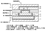
図58に、特許文献1で提案されている半導体装置のCu−Cu接合界面付近の概略構成断面図を示す。特許文献1の半導体装置500は、半導体基板501、配線層503、スルーホール505(縦孔配線部)、絶縁層507、接地配線層509、及び、絶縁材料512を含む第1の半導体部材を備える。また、半導体装置500は、半導体基板502、配線層504、スルーホール506、絶縁層508、接地配線層510、及び、絶縁材料513を含む第2の半導体部材を備える。
FIG. 58 shows a schematic cross-sectional view of the vicinity of the Cu—Cu junction interface of the semiconductor device proposed in Patent Document 1. The semiconductor device 500 of Patent Document 1 includes a first semiconductor member including a semiconductor substrate 501, a wiring layer 503, a through hole 505 (vertical hole wiring portion), an insulating layer 507, a ground wiring layer 509, and an insulating material 512. . The semiconductor device 500 includes a second semiconductor member including a semiconductor substrate 502, a wiring layer 504, a through hole 506, an
第1の半導体部材では、配線層503は、半導体基板501の一方の表面(接合側の表面)に埋め込むように形成される。絶縁層507及び接地配線層509は、この順で、半導体基板501の一方の表面上に積層される。また、スルーホール505は、絶縁層507及び接地配線層509からなる積層膜に形成される。この際、スルーホール505は、積層膜の厚さ方向に沿って、積層膜を貫通するように形成される。なお、スルーホール505の一方の端部は、配線層503に接続され、他方の端部は、第1の半導体部材の接合側の面(接地配線層509側の表面)に露出するように設けられる。さらに、絶縁材料512は、スルーホール505と接地配線層509との間に設けられる。 In the first semiconductor member, the wiring layer 503 is formed so as to be embedded in one surface (surface on the bonding side) of the semiconductor substrate 501. The insulating layer 507 and the ground wiring layer 509 are stacked on one surface of the semiconductor substrate 501 in this order. Further, the through hole 505 is formed in a laminated film including the insulating layer 507 and the ground wiring layer 509. At this time, the through hole 505 is formed so as to penetrate the laminated film along the thickness direction of the laminated film. Note that one end portion of the through hole 505 is connected to the wiring layer 503, and the other end portion is provided so as to be exposed on the surface of the first semiconductor member on the bonding side (surface on the ground wiring layer 509 side). It is done. Further, the insulating material 512 is provided between the through hole 505 and the ground wiring layer 509.
一方、第2の半導体部材では、配線層504は、半導体基板502の一方の表面(接合側の表面)に埋め込むように形成される。絶縁層508及び接地配線層510は、この順で、半導体基板502の一方の表面上に積層される。また、スルーホール506は、絶縁層508及び接地配線層510からなる積層膜に形成される。この際、スルーホール506は、積層膜の厚さ方向に沿って、積層膜を貫通するように形成される。なお、スルーホール506の一方の端部は、配線層504に接続され、他方の端部は、第2の半導体部材の接合側の面(接地配線層510側の表面)に露出するように設けられる。さらに、絶縁材料513は、スルーホール506と接地配線層510との間に設けられる。
On the other hand, in the second semiconductor member, the wiring layer 504 is formed so as to be embedded in one surface (surface on the bonding side) of the semiconductor substrate 502. The
そして、特許文献1では、上記構成の第1の半導体部材の接地配線層509側の表面と、上記構成の第2の半導体部材の接地配線層510側の表面とを接合することにより、半導体装置500が作製される。 In Patent Document 1, a semiconductor device is obtained by bonding the surface of the first semiconductor member having the above configuration on the ground wiring layer 509 side and the surface of the second semiconductor member having the above configuration on the ground wiring layer 510 side. 500 is made.
上述のように、従来、半導体装置の技術分野において、2枚の半導体基板を貼り合わせて、Cu−Cu接合を行う技術が提案されている。しかしながら、この技術分野では、Cu−Cu接合界面(以下、単に接合界面という)における例えば電気特性や密着性などの劣化をより一層抑制して、より信頼性の高い接合界面を有する半導体装置の開発が望まれている。 As described above, conventionally, in the technical field of semiconductor devices, a technique for bonding two semiconductor substrates and performing Cu-Cu bonding has been proposed. However, in this technical field, development of a semiconductor device having a more reliable bonding interface by further suppressing deterioration of, for example, electrical characteristics and adhesion at a Cu-Cu bonding interface (hereinafter simply referred to as a bonding interface). Is desired.
本開示は、上記要望に応えるためになされたものであり、本開示の目的は、より信頼性の高い接合界面を有する半導体装置、電子機器、及び、半導体装置の製造方法を提供することである。 The present disclosure has been made to meet the above-described demand, and an object of the present disclosure is to provide a semiconductor device, an electronic device, and a method for manufacturing the semiconductor device having a more reliable bonding interface. .
上記課題を解決するために、本開示の半導体装置は、接合界面側の表面に形成された第1金属膜を有する第1半導体部と、接合界面で第1金属膜と接合されかつこの接合界面側の表面面積が第1金属膜の接合界面側の表面面積より小さい第2金属膜を有し、接合界面で第1半導体部と貼り合わせて設けられた第2半導体部と、第1金属膜の接合界面側の面領域のうち第2金属膜と接合しない面領域を含む領域に設けられた界面バリア部と、を備える。
そして、界面バリア部は、接合界面で第1半導体部と接合されるべく第2金属膜と面一に形成される、絶縁体の界面バリア膜により構成され、第2半導体部は、第2金属膜の側部を覆うように設けられた絶縁膜を有し、界面バリア膜が、絶縁膜の接合界面側の表面に形成される。
In order to solve the above problems, a semiconductor device of the present disclosure includes a first semiconductor section including a first metal film formed on the surface of the bonding interface side, is bonded to the first metal layer at the bonding interface and the bonding interface A second semiconductor part having a second metal film whose surface area on the side is smaller than the surface area on the bonding interface side of the first metal film, and is provided by being bonded to the first semiconductor part at the bonding interface; And an interface barrier portion provided in a region including a surface region that is not bonded to the second metal film in the surface region on the bonding interface side.
The interface barrier portion is formed of an insulating interface barrier film formed flush with the second metal film so as to be bonded to the first semiconductor portion at the bonding interface . An insulating film is provided so as to cover the side of the metal film, and an interface barrier film is formed on the surface of the insulating film on the bonding interface side .
また、本開示の電子機器は、上記本開示の半導体装置と、半導体装置の出力信号を処理する信号処理回路とを備える構成とする。 In addition, an electronic apparatus of the present disclosure includes the semiconductor device of the present disclosure and a signal processing circuit that processes an output signal of the semiconductor device.
さらに、本開示の半導体装置の製造方法は、以下に示す手順で行う。
まず、接合界面側の表面に形成された第1金属膜を有する第1半導体部を作製する。次に、接合界面側の表面面積が第1金属膜の接合界面側の表面面積より小さい第2金属膜と、第1金属膜の接合界面側の面領域のうち第2金属膜と接合しない面領域を含む領域に、接合界面で第1半導体部と接合されるべく第2金属膜と面一に形成される、絶縁体の界面バリア膜により構成される界面バリア部とを有し、第2金属膜の側部を覆うように設けられた絶縁膜を有し、界面バリア膜が、絶縁膜の接合界面側の表面に形成される、第2半導体部を作製する。次いで、第1半導体部の第1金属膜側の表面と第2半導体部の第2金属膜側の表面とを貼り合わせて、第1金属膜と第2金属膜とを接合するステップ。
Furthermore, the manufacturing method of the semiconductor device of this indication is performed in the procedure shown below.
First, a first semiconductor part having a first metal film formed on the surface on the bonding interface side is produced. Next, the second metal film whose surface area on the bonding interface side is smaller than the surface area on the bonding interface side of the first metal film, and the surface not bonded to the second metal film in the surface area on the bonding interface side of the first metal film in the region including the region, it is formed on the second metal film flush to be bonded to the first semiconductor portion at the bonding interface, and a configured surface barrier section by an interfacial barrier film insulator, second A second semiconductor part is manufactured , which has an insulating film provided so as to cover the side part of the metal film, and the interface barrier film is formed on the surface of the insulating film on the bonding interface side . Then, by bonding the first metal layer-side surface of the first semiconductor section and the second metal layer side of the surface of the second semiconductor section, join the first metal film and the second metal layer step.
上述のように、本開示の半導体装置(電子機器)、及び、その製造方法では、第1金属膜と接合する第2金属膜の接合側の表面面積を、第1金属膜の接合側の表面面積より小さくする。そして、第1金属膜の接合界面側の面領域のうち第2金属膜と接合しない面領域を含む領域に界面バリア部を設ける。この本開示の構成によれば、接合界面における電気特性の劣化をより一層抑制して、より信頼性の高い接合界面を有する半導体装置(電子機器)、及び、その製造方法を提供することができる。 As described above, in the semiconductor device (electronic device) and the manufacturing method thereof according to the present disclosure, the surface area on the bonding side of the second metal film bonded to the first metal film is defined as the surface on the bonding side of the first metal film. Make it smaller than the area. Then, an interface barrier portion is provided in a region including a surface region that is not bonded to the second metal film in the surface region on the bonding interface side of the first metal film. According to the configuration of the present disclosure, it is possible to provide a semiconductor device (electronic device) having a more reliable bonding interface and a method for manufacturing the same, further suppressing deterioration of electrical characteristics at the bonding interface. .
以下に、本開示の実施形態に係る半導体装置、及び、その製造手法の例を、図面を参照しながら下記の順で説明する。ただし、本開示は下記の例に限定されない。
1.第1の実施形態
2.第2の実施形態
3.第3の実施形態
4.各種変形例及び参考例
5.第4の実施形態
6.第5の実施形態
7.各種応用例
Hereinafter, a semiconductor device according to an embodiment of the present disclosure and an example of a manufacturing method thereof will be described in the following order with reference to the drawings. However, the present disclosure is not limited to the following example.
1.
<1.第1の実施形態>
[従来のCu−Cu接合技術の問題点]
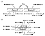
まず、本開示の第1の実施形態に係る半導体装置について説明する前に、従来のCu−Cu接合技術で発生し得る問題点を、図1(a)及び(b)、並びに、図2を参照しながら説明する。なお、図1(a)は、2つの半導体部材を接合する前の各半導体部材の概略構成断面図であり、図1(b)は、接合後の接合界面付近の概略断面図である。また、図2は、2つの半導体部材の貼り合わせ時に接合アライメントずれが発生した場合に発生し得る問題を説明するための図である。
<1. First Embodiment>
[Problems of conventional Cu-Cu bonding technology]
First, before describing the semiconductor device according to the first embodiment of the present disclosure, problems that may occur in the conventional Cu-Cu bonding technique are illustrated in FIGS. 1 (a) and 1 (b), and FIG. The description will be given with reference. 1A is a schematic cross-sectional view of each semiconductor member before joining the two semiconductor members, and FIG. 1B is a schematic cross-sectional view of the vicinity of the joined interface after joining. FIG. 2 is a diagram for explaining a problem that may occur when bonding misalignment occurs when two semiconductor members are bonded.
ここでは、第1SiO2層611、第1Cu電極612、及び、第1Cuバリア層613を含む第1半導体部材610と、第2SiO2層621、第2Cu電極622、及び、第2Cuバリア層623を含む第2半導体部材620とを接合する例を示す。
Here, the first semiconductor member 610 including the first SiO 2 layer 611, the first Cu electrode 612, and the first Cu barrier layer 613, and the second SiO 2 layer 621, the second Cu electrode 622, and the second Cu barrier layer 623 are included. The example which joins the
なお、図1(a)及び(b)に示す例では、各半導体部材において、Cu電極は、SiO2層の一方の表面に埋め込むようにして形成される。すなわち、Cu電極は、SiO2層の一方の表面に露出し、かつ、その露出面がSiO2層の一方の表面と略面一となるように形成される。また、Cuバリア層は、Cu電極とSiO2層との間に設けられる。そして、第1半導体部材610の第1Cu電極612側の表面と、第2半導体部材620の第2Cu電極622側の表面とが貼り合わされる。
In the example shown in FIGS. 1A and 1B, in each semiconductor member, the Cu electrode is formed so as to be embedded in one surface of the SiO 2 layer. That is, the Cu electrode is formed so as to be exposed on one surface of the SiO 2 layer, and the exposed surface thereof is substantially flush with the one surface of the SiO 2 layer. The Cu barrier layer is provided between the Cu electrode and the SiO 2 layer. Then, the surface of the first semiconductor member 610 on the first Cu electrode 612 side and the surface of the
第1半導体部材610と第2半導体部材620とを接合する際、両者の間に接合アライメントずれが発生すると、図1(b)に示すように、接合界面Sjにおいて、一方の半導体部材のCu電極と他方の半導体部材のSiO2層との接触領域が生成される。
When joining of the first semiconductor member 610 and the
この場合、接合時のアニール処理等により、図2に示すように、各Cu電極からSiO2層にCu630が拡散し、接合界面Sjにおいて、隣り合うCu電極間が短絡する可能性がある。また、各Cu電極からSiO2層へのCu630の拡散量が大きいとCu電極内のCuの量が減るので、例えば、接触抵抗の上昇や導通不良などの不具合が生じる場合も考えられる。 In this case, as shown in FIG. 2, Cu630 diffuses from each Cu electrode to the SiO 2 layer due to an annealing process at the time of bonding, and adjacent Cu electrodes may be short-circuited at the bonding interface Sj. In addition, if the amount of Cu630 diffused from each Cu electrode to the SiO 2 layer is large, the amount of Cu in the Cu electrode is reduced. For example, problems such as an increase in contact resistance and poor conduction may occur.
上述のような接合界面Sjにおける電気特性の不具合が生じると、半導体装置の性能が劣化する。そこで、本実施形態では、上述のような接合界面Sjにおける電気特性の不具合を解消することができる半導体装置の構成について説明する。 When a defect in the electrical characteristics at the bonding interface Sj as described above occurs, the performance of the semiconductor device deteriorates. In view of this, in the present embodiment, a configuration of a semiconductor device capable of eliminating the above-described defects in electrical characteristics at the bonding interface Sj will be described.
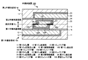
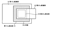
[半導体装置の構成]
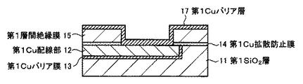
図3及び4に、第1の実施形態に係る半導体装置の概略構成を示す。図3は、第1の実施形態の半導体装置の接合界面付近の概略断面図であり、図4は、各Cu接合部及び後述の界面Cuバリア膜間の配置関係を示す接合界面付近の概略上面図である。なお、図3及び4では、説明を簡略化するため、1つの接合界面付近の構成のみを示す。
[Configuration of semiconductor device]
3 and 4 show a schematic configuration of the semiconductor device according to the first embodiment. FIG. 3 is a schematic cross-sectional view in the vicinity of the bonding interface of the semiconductor device of the first embodiment, and FIG. FIG. In FIGS. 3 and 4, only the configuration near one bonding interface is shown to simplify the description.
半導体装置1は、図3に示すように、第1半導体部材10(第1半導体部)と、第2半導体部材20(第2半導体部)とを備える。そして、本実施形態の半導体装置1では、第1半導体部材10の後述する第1層間絶縁膜15側の面が、第2半導体部材20の後述する界面Cuバリア膜28側の面と接合される。
As shown in FIG. 3, the semiconductor device 1 includes a first semiconductor member 10 (first semiconductor portion) and a second semiconductor member 20 (second semiconductor portion). In the semiconductor device 1 of the present embodiment, the surface of the first semiconductor member 10 on the first
第1半導体部材10は、第1半導体基板(不図示)、第1SiO2層11、第1Cu配線部12、第1Cuバリア膜13、第1Cu拡散防止膜14、第1層間絶縁膜15、第1Cu接合部16、及び、第1Cuバリア層17を有する。
The first semiconductor member 10 includes a first semiconductor substrate (not shown), a first SiO 2 layer 11, a first
第1SiO2層11は、第1半導体基板上に形成される。第1Cu配線部12は、第1SiO2層11の第1半導体基板側とは反対側の表面に埋め込むようにして形成される。なお、第1Cu配線部12は、図4に示すように、所定方向に延在したCu膜であり、例えば、図示しない半導体装置1内及び/又は半導体装置1を含む電子機器内の所定のデバイス、信号処理回路等に接続される。
The first SiO 2 layer 11 is formed on the first semiconductor substrate. The first
第1Cuバリア膜13は、第1SiO2層11と第1Cu配線部12との間に形成される。なお、第1Cuバリア膜13は、第1Cu配線部12から第1SiO2層11へのCu(銅)の拡散を防止するための薄膜であり、例えば、Ti、Ta、Ru、又は、それらの窒化物(TiN、TaN、RuN)で形成される。
The first
第1Cu拡散防止膜14は、第1SiO2層11及び第1Cu配線部12の領域上であり、かつ、第1Cuバリア層17の形成領域以外の領域上に形成される。なお、第1Cu拡散防止膜14は、第1Cu配線部12から第1層間絶縁膜15へのCuの拡散を防止するための薄膜であり、例えばSiC、SiN、又は、SiCN等の薄膜で構成される。
The first Cu
第1層間絶縁膜15は、第1Cu拡散防止膜14上に形成され、例えばSiO2膜等の酸化膜で構成される。
The first
第1Cu接合部16(第1金属膜)は、第1層間絶縁膜15の第1Cu拡散防止膜14側とは反対側の表面に埋め込むようにして設けられる。なお、本実施形態では、第1Cu接合部16を、図4に示すように、表面(膜面)が正方形状のCu膜で構成する。ただし、本開示はこれに限定されず、第1Cu接合部16の表面形状は、例えば、必要とする接触抵抗、デザインルール等の条件を考慮して適宜変更することができる。
The first Cu bonding portion 16 (first metal film) is provided so as to be embedded on the surface of the first
第1Cuバリア層17は、第1Cu接合部16と、第1Cu配線部12、第1Cu拡散防止膜14及び第1層間絶縁膜15との間に設けられ、第1Cu接合部16を覆うように設けられる。これにより、第1Cu接合部16は、第1Cuバリア層17を介して第1Cu配線部12に電気的に接続される。なお、第1Cuバリア層17は、第1Cu接合部16から第1層間絶縁膜15へのCuの拡散を防止するための薄膜であり、例えば、Ti、Ta、Ru、又は、それらの窒化物で形成される。
The first
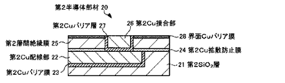
第2半導体部材20は、第2半導体基板(不図示)、第2SiO2層21、第2Cu配線部22、第2Cuバリア膜23、第2Cu拡散防止膜24、第2層間絶縁膜25、第2Cu接合部26、第2Cuバリア層27、及び、界面Cuバリア膜28を有する。
The
なお、本実施形態では、第2半導体部材20の第2半導体基板、第2SiO2層21、及び、第2Cu配線部22は、それぞれ、第1半導体部材10の第1半導体基板、第1SiO2層11、及び、第1Cu配線部12と同様の構成である。また、第2半導体部材20の第2Cuバリア膜23、第2Cu拡散防止膜24、及び、第2層間絶縁膜25は、それぞれ、第1半導体部材10の第1Cuバリア膜13、第1Cu拡散防止膜14、及び、第1層間絶縁膜15と同様の構成である。
In the present embodiment, the second semiconductor substrate, the second SiO 2 layer 21 and the second
第2Cu接合部26(第2金属膜)は、第2層間絶縁膜25(絶縁膜)の第2Cu拡散防止膜24側とは反対側の表面に埋め込むようにして設けられる。なお、本実施形態では、第2Cu接合部26を、図4に示すように、表面が正方形状のCu膜で構成する。ただし、本開示はこれに限定されず、第2Cu接合部26の表面形状は、例えば、必要とする接触抵抗、デザインルール等の条件を考慮して適宜変更することができる。
The second Cu bonding portion 26 (second metal film) is provided so as to be embedded on the surface of the second interlayer insulating film 25 (insulating film) opposite to the second Cu
また、本実施形態では、図3及び4に示すように、第2Cu接合部26の接合側(接合界面Sj側)の表面面積(接合側表面の寸法)を、第1Cu接合部16のそれより小さくする。この際、第1半導体部材10及び第2半導体部材20間で想定される最大の接合アライメントずれが発生しても、接合界面Sjにおいて、第2Cu接合部26と第1層間絶縁膜15とが接触しないように、第2Cu接合部26のサイズを設定する。より具体的には、例えば、図3に示すように、第2Cu接合部26の側面と第1Cuバリア層17の側面との最短距離をΔaとしたとき、Δaが想定される最大の接合アライメントずれ以上の寸法となるように、第2Cu接合部26のサイズを設定する。
In this embodiment, as shown in FIGS. 3 and 4, the surface area (dimension of the surface on the bonding side) on the bonding side (bonding interface Sj side) of the second
第2Cuバリア層27は、第2Cu接合部26と、第2Cu配線部22、第2Cu拡散防止膜24及び第2層間絶縁膜25との間に設けられ、第2Cu接合部26を覆うように設けられる。これにより、第2Cu接合部26は、第2Cuバリア層27を介して第2Cu配線部22に電気的に接続される。なお、第2Cuバリア層27は、第1Cuバリア層17と同様に、第2Cu接合部26から第2層間絶縁膜25へのCuの拡散を防止するための薄膜であり、例えば、Ti、Ta、Ru、又は、それらの窒化物で形成される。
The second
界面Cuバリア膜28(界面バリア膜、界面バリア部)は、第2層間絶縁膜25上に形成される。この際、界面Cuバリア膜28の表面と、第2Cu接合部26の接合側の表面とが略面一となるように、界面Cuバリア膜28を形成する。すなわち、界面Cuバリア膜28は、第1Cu接合部16の接合界面Sj側の面領域のうち第2Cu接合部26と接合しない面領域を含む領域に設けられる。このような領域(位置)に界面Cuバリア膜28を設けることにより、接合界面Sjにおける第1Cu接合部16と第2層間絶縁膜25との対向領域を介して、Cu接合部から層間絶縁膜(SiO2膜)にCuが拡散することを防止することができる。
The interface Cu barrier film 28 (interface barrier film, interface barrier part) is formed on the second
なお、界面Cuバリア膜28は、例えば、SiN、SiON、SiCN、有機系樹脂等の材料で形成することができる。ただし、Cu膜との密着性向上という観点では、特に、界面Cuバリア膜28をSiNで形成することが好ましい。
The interface
[半導体装置の製造手法]
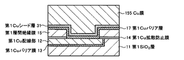
次に、本実施形態の半導体装置1の製造手法を、図5〜17を参照しながら説明する。なお、図5〜16には、各工程で作製される半導体部材のCu接合部付近の概略断面を示し、図17には、第1半導体部材10と第2半導体部材20との接合処理の様子を示す。
[Semiconductor Device Manufacturing Method]
Next, a method for manufacturing the semiconductor device 1 according to the present embodiment will be described with reference to FIGS. FIGS. 5 to 16 show schematic cross sections near the Cu bonding portion of the semiconductor member manufactured in each step, and FIG. 17 illustrates the bonding process between the first semiconductor member 10 and the
最初に、図5〜10を参照しながら、第1半導体部材10の作製手法を説明する。本実施形態では、図示しないが、まず、第1SiO2層11(下地絶縁層)の一方の表面の所定領域に、第1Cuバリア膜13、及び、第1Cu配線部12をこの順で形成する。この際、第1Cu配線部12を、第1SiO2層11の一方の表面に埋め込むように(第1Cu配線部12が該表面に露出するように)形成する。
First, a manufacturing method of the first semiconductor member 10 will be described with reference to FIGS. In this embodiment, although not shown, first, a first
次いで、図5に示すように、第1SiO2層11、第1Cu配線部12、及び、第1Cuバリア膜13からなる半導体部材の第1Cu配線部12側の表面上に、第1Cu拡散防止膜14を形成する。なお、第1SiO2層11、第1Cu配線部12、第1Cuバリア膜13、及び、第1Cu拡散防止膜14は、従来の例えば固体撮像装置等の半導体装置の製造手法(例えば特開2004−63859号公報参照)と同様にして形成することができる。
Next, as shown in FIG. 5, the first Cu
次いで、第1Cu拡散防止膜14上に、第1層間絶縁膜15を形成する。具体的には、例えば、第1Cu拡散防止膜14上に、厚さが約50〜500nm程度のSiO2膜又は炭素含有酸化シリコン(SiOC)膜を成膜して第1層間絶縁膜15を形成する。なお、このような第1層間絶縁膜15は、例えばCVD(Chemical Vapor Deposition)法、又は、スピンコート法で形成することができる。
Next, a first
次いで、図6に示すように、第1層間絶縁膜15上にレジスト膜150を形成する。そして、フォトリソグラフィ技術を用いて、レジスト膜150に対してパターニング処理を施し、第1Cu接合部16の形成領域のレジスト膜150を除去して開口部150aを形成する。
Next, as shown in FIG. 6, a resist film 150 is formed on the first
次いで、レジスト膜150が形成された半導体部材の開口部150a側の表面に対して、例えば従来既知のマグネトロン方式のエッチング装置を用いて、ドライエッチング処理を行う。これにより、レジスト膜150の開口部150aに露出した第1層間絶縁膜15の領域がエッチングされる。このエッチング処理では、図7に示すように、レジスト膜150の開口部150aの領域の第1層間絶縁膜15、及び、第1Cu拡散防止膜14を除去し、第1層間絶縁膜15の開口部15aに第1Cu配線部12を露出させる。なお、本実施形態では、第1層間絶縁膜15の開口部15aの開口径を、例えば、約4〜100μm程度とする。
Next, dry etching is performed on the surface of the semiconductor member on which the resist film 150 is formed on the side of the opening 150a using, for example, a conventionally known magnetron etching apparatus. Thereby, the region of the first
その後、エッチング処理された面に対して、例えば酸素(O2)プラズマを用いたアッシング処理、及び、有機アミン系の薬液を用いた洗浄処理を施す。これにより、第1層間絶縁膜15上に残留したレジスト膜150、及び、上記エッチング処理で発生した残留付着物を除去する。
Thereafter, the etched surface is subjected to, for example, an ashing process using oxygen (O 2 ) plasma and a cleaning process using an organic amine chemical solution. Thereby, the resist film 150 remaining on the first
次いで、図8に示すように、第1層間絶縁膜15上、及び、第1層間絶縁膜15の開口部15aに露出した第1Cu配線部12上に、Ti、Ta、Ru、又は、それらの窒化物からなる第1Cuバリア層17を形成する。具体的には、例えばRF(Radio Frequency)スパッタリング法等の手法を用いて、Ar/N2雰囲気中で、厚さが約5〜50nmの第1Cuバリア層17を、第1層間絶縁膜15及び第1Cu配線部12上に形成する。
Next, as shown in FIG. 8, Ti, Ta, Ru, or those on the first
次いで、図9に示すように、第1Cuバリア層17上に、例えばスパッタリング法及び電解メッキ法等の手法を用いて、Cu膜151を形成する。この処理により、第1層間絶縁膜15の開口部15aの領域にCu膜151が埋め込まれる。
Next, as shown in FIG. 9, a Cu film 151 is formed on the first
次いで、Cu膜151が形成された半導体部材を、例えばホットプレートやシンターアニール装置等の加熱装置を用いて、窒素雰囲気中又は真空中で、約100〜400℃で1〜60分程度加熱する。この加熱処理により、Cu膜151を引き締めて緻密な膜質のCu膜151を形成する。 Next, the semiconductor member on which the Cu film 151 is formed is heated at about 100 to 400 ° C. for about 1 to 60 minutes in a nitrogen atmosphere or in vacuum using a heating device such as a hot plate or a sinter annealing device. By this heat treatment, the Cu film 151 is tightened to form a dense Cu film 151.
その後、図10に示すように、Cu膜151及び第1Cuバリア層17の不要な部分を化学機械研磨(CMP)法により除去する。具体的には、第1層間絶縁膜15が表面に露出するまで、Cu膜151側の表面をCMP法で研磨する。
Thereafter, as shown in FIG. 10, unnecessary portions of the Cu film 151 and the first
本実施形態では、上述した図5〜10の各種工程を行い、第1半導体部材10を作製する。次に、第2半導体部材20の作製手法を、図11〜16を参照しながら説明する。
In this embodiment, the various processes of FIGS. 5 to 10 described above are performed to produce the first semiconductor member 10. Next, a method for manufacturing the
まず、第1半導体部材10と同様にして(図5の工程)、第2SiO2層21の一方の表面の所定領域に、第2Cuバリア膜23、及び、第2Cu配線部22をこの順で形成する。次いで、第2SiO2層21、第2Cu配線部22、及び、第2Cuバリア膜23からなる半導体部材の第2Cu配線部22側の表面上に、第2Cu拡散防止膜24を形成する。
First, similarly to the first semiconductor member 10 (step of FIG. 5), a second
次いで、第2Cu拡散防止膜24上に、第2層間絶縁膜25を形成する。具体的には、例えば、第2Cu拡散防止膜24上に、厚さが約50〜500nm程度のSiO2膜又はSiOC膜を成膜して第2層間絶縁膜25を形成する。なお、このような第2層間絶縁膜25は、例えばCVD法又はスピンコート法で形成することができる。次いで、第2層間絶縁膜25上に、例えばCVD法又はスピンコート法等の手法を用いて、厚さが約5〜100nm程度の界面Cuバリア膜28を形成する。次いで、界面Cuバリア膜28上に、例えばCVD法又はスピンコート法等の手法を用いて、厚さが約50〜200nm程度のSiO2膜又はSiOC膜を成膜して絶縁膜152を形成する。
Next, a second
次いで、図11に示すように、絶縁膜152上にレジスト膜153を形成する。そして、フォトリソグラフィ技術を用いて、レジスト膜153に対してパターニング処理を施し、第2Cu接合部26の形成領域のレジスト膜153を除去して開口部153aを形成する。なお、開口部153aの開口径は、図6の工程で形成したレジスト膜150の開口部150aのそれより小さくする。
Next, as illustrated in FIG. 11, a resist film 153 is formed over the insulating film 152. Then, a patterning process is performed on the resist film 153 by using a photolithography technique, and the resist film 153 in the formation region of the second
ただし、上述したレジスト膜153に開口部153aが形成された半導体部材の作製工程は、図11に示す例に限定されず、例えば、界面Cuバリア膜28上に直接、レジスト膜153を設け、さらに、開口部153aを形成してもよい。図12に、その手法で開口部153aを形成した際の半導体部材の概略断面図を示す。
However, the manufacturing process of the semiconductor member in which the opening 153a is formed in the resist film 153 described above is not limited to the example illustrated in FIG. 11. For example, the resist film 153 is provided directly on the interface
ただし、図12に示す手法を採用した場合、界面Cuバリア膜28上に直接、第2Cuバリア層27を介してCu膜が形成され、その後、該Cu膜をCMP処理で研磨することにより第2Cu接合部26が形成される。しかしながら、通常、界面Cuバリア膜28はCMP処理で研磨することが難しい膜であるので、図12に示す手法を採用した場合には、CMP処理時に、Cu膜の削り残しが界面Cuバリア膜28上に発生する場合もある。
However, when the technique shown in FIG. 12 is adopted, a Cu film is formed directly on the interface
それに対して、図11に示す開口部153aの形成手法では、界面Cuバリア膜28上に絶縁膜152が形成されるので、Cu膜のCMP処理時に絶縁膜152も一緒に研磨することにより、Cu膜の削り残しをより確実に無くすことができる。すなわち、第2Cu接合部26を形成する際のCu膜の削り残しを防止する観点では、図11に示す開口部153aの形成手法が図12に示す開口部153aの形成手法より好適である。
In contrast, in the method of forming the opening 153a shown in FIG. 11, since the insulating film 152 is formed on the interface
次いで、レジスト膜153が形成された半導体部材の開口部153a側の表面に対して、例えば従来既知のマグネトロン方式のエッチング装置を用いて、ドライエッチング処理を行う。これにより、レジスト膜153の開口部153aに露出した絶縁膜152の領域がエッチングされる。このエッチング処理では、図13に示すように、開口部153aの領域の絶縁膜152、界面Cuバリア膜28、第2層間絶縁膜25、及び、第2Cu拡散防止膜24を除去し、第2層間絶縁膜25の開口部25aに第2Cu配線部22を露出させる。なお、本実施形態では、第2層間絶縁膜25の開口部25aの開口径は、例えば、約1〜95μm程度とする。
Next, a dry etching process is performed on the surface of the semiconductor member on which the resist film 153 is formed on the opening 153a side using, for example, a conventionally known magnetron etching apparatus. Thereby, the region of the insulating film 152 exposed in the opening 153a of the resist film 153 is etched. In this etching process, as shown in FIG. 13, the insulating film 152, the interfacial
その後、エッチング処理された面に対して、例えば酸素(O2)プラズマを用いたアッシング処理、及び、有機アミン系の薬液を用いた洗浄処理を施す。これにより、絶縁膜152上に残留したレジスト膜153、及び、上記エッチング処理で発生した残留付着物を除去する。 Thereafter, the etched surface is subjected to, for example, an ashing process using oxygen (O 2 ) plasma and a cleaning process using an organic amine chemical solution. As a result, the resist film 153 remaining on the insulating film 152 and the residual deposit generated in the etching process are removed.
次いで、図14に示すように、絶縁膜152上、及び、第2層間絶縁膜25の開口部25aに露出した第2Cu配線部22上に、Ti、Ta、Ru、又は、それらの窒化物からなる第2Cuバリア層27を形成する。具体的には、例えばRFスパッタリング法等の手法を用いて、Ar/N2雰囲気中で、厚さが約5〜50nmの第2Cuバリア層27を、絶縁膜152及び第2Cu配線部22上に形成する。
Next, as shown in FIG. 14, Ti, Ta, Ru, or a nitride thereof is formed on the insulating film 152 and on the second
次いで、図15に示すように、第2Cuバリア層27上に、例えばスパッタリング法及び電解メッキ法等の手法を用いて、Cu膜154を形成する。この処理により、第2層間絶縁膜25の開口部25aの領域にCu膜154が埋め込まれる。
Next, as shown in FIG. 15, a Cu film 154 is formed on the second
次いで、Cu膜154が形成された半導体部材を、例えばホットプレートやシンターアニール装置等の加熱装置を用いて、窒素雰囲気中又は真空中で、約100〜400℃で1〜60分程度加熱する。この加熱処理により、Cu膜154を引き締めて緻密な膜質のCu膜154を形成する。 Next, the semiconductor member on which the Cu film 154 is formed is heated at about 100 to 400 ° C. for about 1 to 60 minutes in a nitrogen atmosphere or in vacuum using a heating apparatus such as a hot plate or a sinter annealing apparatus. By this heat treatment, the Cu film 154 is tightened to form a dense Cu film 154.
そして、図16に示すように、Cu膜154、第2Cuバリア層27及び絶縁膜152の不要な部分を化学機械研磨(CMP)法により除去する。具体的には、界面Cuバリア膜28が表面に露出するまで、Cu膜154側の表面をCMP法で研磨する。本実施形態では、上述した図11〜16の各種工程を行い、第2半導体部材20を作製する。
Then, as shown in FIG. 16, unnecessary portions of the Cu film 154, the second
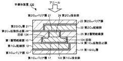
次いで、上記手順で作製された第1半導体部材10(図10)と第2半導体部材20(図16)とを貼り合わせる。この貼り合わせ工程(接合工程)の具体的な処理内容は、次の通りである。 Next, the first semiconductor member 10 (FIG. 10) and the second semiconductor member 20 (FIG. 16) manufactured by the above procedure are bonded together. The specific processing content of this bonding process (joining process) is as follows.
まず、第1半導体部材10の第1Cu接合部16側の表面、及び、第2半導体部材20の第2Cu接合部26側の表面に対して還元処理を施し、各Cu接合部の表面の酸化膜(酸化物)を除去する。これにより、各Cu接合部の表面に清浄なCuを露出させる。なお、この際、還元処理としては、例えば蟻酸等の薬液を用いたウェットエッチング処理、又は、例えばAr、NH3、H2等のプラズマを用いたドライエッチング処理が用いられる。
First, a reduction process is performed on the surface of the first semiconductor member 10 on the first
次いで、図17に示すように、第1半導体部材10の第1Cu接合部16側の表面と、第2半導体部材20の第2Cu接合部26側の表面とを接触させる(貼り合わせる)。この際、第1Cu接合部16と、それに対応する第2Cu接合部26とが対向するように位置合わせを行ってから両者を貼り合わせる。
Next, as shown in FIG. 17, the surface of the first semiconductor member 10 on the first
次いで、第1半導体部材10及び第2半導体部材20を貼り合わせた状態で、例えばホットプレートやRTA(Rapid Thermal Annealing)装置等の加熱装置を用いて貼り合わせ部材をアニールして、第1Cu接合部16と第2Cu接合部26とを接合する。具体的には、例えば、大気圧のN2雰囲気中、又は、真空中で約100〜400℃で5分〜2時間程度、貼り合わせ部材を加熱する。
Next, in a state where the first semiconductor member 10 and the
また、この接合処理により、第1Cu接合部16の接合界面Sj側の面領域のうち第2Cu接合部26と接合しない面領域を含む領域に界面Cuバリア膜28が配置される。より具体的には、図3に示すように、第1Cu接合部16と、第2層間絶縁膜25とが対向する接合界面Sjの領域を含む領域に界面Cuバリア膜28が配置される。
Further, by this bonding process, the interface
本実施形態では、このようにして、Cu−Cu接合処理を行う。なお、上述した接合工程以外の半導体装置1の製造工程は、従来の例えば固体撮像装置等の半導体装置の製造手法(例えば特開2007−234725号公報参照)と同様にすることができる。 In this embodiment, the Cu—Cu bonding process is performed in this way. The manufacturing process of the semiconductor device 1 other than the above-described bonding process can be the same as the conventional manufacturing method of a semiconductor device such as a solid-state imaging device (see, for example, Japanese Patent Application Laid-Open No. 2007-234725).
上述のように、本実施形態の半導体装置1では、第1半導体部材10の第1Cu接合部16と、第2半導体部材20の第2層間絶縁膜25とが対向する接合界面領域を含む領域には、界面Cuバリア膜28が設けられる。それゆえ、本実施形態では、半導体部材の接合時に、接合アライメントずれが発生しても、接合界面Sjにおいて、Cu接合部と層間絶縁膜との接触領域が発生せず、上述した接合界面Sjにおける電気特性の不具合を解消することができる。
As described above, in the semiconductor device 1 of this embodiment, the
また、本実施形態では、上述のように、第1Cu接合部16の接合側の表面面積を、第2Cu接合部26のそれより十分大きくする。それゆえ、本実施形態では、第1半導体部材10及び第2半導体部材20の接合時に接合アライメントずれが発生しても、Cu接合部間の接触面積(接触抵抗)は変化せず、半導体装置1の電気特性(性能)の劣化を抑制することができる。すなわち、本実施形態では、接合界面Sjにおける接触抵抗の増大を抑制することができるので、半導体装置1の消費電力の増大、及び、処理速度の遅延を抑制することができる。
Further, in the present embodiment, as described above, the surface area on the bonding side of the first
さらに、本実施形態では、第1Cu接合部16と第2層間絶縁膜25との間には、界面Cuバリア膜28が設けられるので、両者間の密着力を向上させることができる。これにより、本実施形態では、第1半導体部材10及び第2半導体部材20間の接合強度を増大させることができる。
Furthermore, in this embodiment, since the interface
以上のことから、本実施形態では、接合界面における電気特性の劣化をより一層抑制することができ、より信頼性の高い接合界面Sjを有する半導体装置1を提供することができる。 From the above, in the present embodiment, it is possible to further suppress the deterioration of the electrical characteristics at the bonding interface, and it is possible to provide the semiconductor device 1 having the bonding interface Sj with higher reliability.
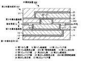
<2.第2の実施形態>
[半導体装置の構成]
図18及び19に、第2の実施形態に係る半導体装置の概略構成を示す。図18は、第2の実施形態に係る半導体装置の接合界面付近の概略断面図であり、図19は、各Cu接合部及び界面Cuバリア膜間の配置関係を示す接合界面付近の概略上面図である。なお、図18及び19では、説明を簡略化するため、1つの接合界面付近の構成のみを示す。また、図18及び19に示す本実施形態の半導体装置2において、図3及び4に示す第1の実施形態の半導体装置1と同様の構成には、同じ符号を付して示す。
<2. Second Embodiment>
[Configuration of semiconductor device]
18 and 19 show a schematic configuration of the semiconductor device according to the second embodiment. 18 is a schematic cross-sectional view in the vicinity of the bonding interface of the semiconductor device according to the second embodiment, and FIG. It is. 18 and 19 show only the configuration near one joint interface for the sake of simplicity. Further, in the
半導体装置2は、図18に示すように、第1半導体部材30(第1半導体部)と、第2半導体部材40(第2半導体部)と、界面Cuバリア膜50(界面バリア膜、界面バリア部)とを備える。
As shown in FIG. 18, the
第1半導体部材30は、第1半導体基板(不図示)、第1SiO2層11、第1Cu配線部12、第1Cuバリア膜13、第1Cu拡散防止膜14、第1層間絶縁膜15、第1Cu接合部16、第1Cuバリア層17、及び、第1Cuシード層31を有する。
The first semiconductor member 30 includes a first semiconductor substrate (not shown), a first SiO 2 layer 11, a first
図18と図3との比較から明らかなように、本実施形態の第1半導体部材30は、第1の実施形態の第1半導体部材10において、第1Cu接合部16と第1Cuバリア層17との間に第1Cuシード層31を設けた構成となる。それ以外の第1半導体部材30の構成は、上記第1の実施形態の第1半導体部材10の対応する構成と同様である。それゆえ、ここでは、第1Cuシード層31の構成についてのみ説明する。 As is clear from a comparison between FIG. 18 and FIG. 3, the first semiconductor member 30 of the present embodiment is the same as the first semiconductor member 10 of the first embodiment. The first Cu seed layer 31 is provided between them. The other configuration of the first semiconductor member 30 is the same as the corresponding configuration of the first semiconductor member 10 of the first embodiment. Therefore, only the configuration of the first Cu seed layer 31 will be described here.
第1Cuシード層31(シード層)は、上述のように、第1Cu接合部16と第1Cuバリア層17との間に設けられ、第1Cu接合部16を覆うように形成される。
As described above, the first Cu seed layer 31 (seed layer) is provided between the
第1Cuシード層31は、酸素と反応し易い金属材料を含有するCu層(Cu合金層)で形成される。第1Cuシード層31に含有する金属材料としては、例えば、酸素に対して水素よりも反応し易い金属材料を用いることができる。具体的には、Fe、Mn、V、Cr、Mg、Si、Ce、Ti、Al等の金属材料を用いることができる。なお、これらの金属材料のうち、Mn、Mg、Ti、又は、Alは、半導体装置に好適な材料である。さらに、接合界面Siの配線抵抗の低下という観点では、第1Cuシード層31に含有する金属材料として、Mn、又は、Tiを用いることが特に好ましい。 The first Cu seed layer 31 is formed of a Cu layer (Cu alloy layer) containing a metal material that easily reacts with oxygen. As the metal material contained in the first Cu seed layer 31, for example, a metal material that reacts more easily with oxygen than oxygen can be used. Specifically, metal materials such as Fe, Mn, V, Cr, Mg, Si, Ce, Ti, and Al can be used. Of these metal materials, Mn, Mg, Ti, or Al is a material suitable for a semiconductor device. Further, from the viewpoint of reducing the wiring resistance of the bonding interface Si, it is particularly preferable to use Mn or Ti as the metal material contained in the first Cu seed layer 31.
第2半導体部材40は、第2半導体基板(不図示)、第2SiO2層21、第2Cu配線部22、第2Cuバリア膜23、第2Cu拡散防止膜24、第2層間絶縁膜25、第2Cu接合部26、第2Cuバリア層27、及び、第2Cuシード層41を有する。
The second semiconductor member 40 includes a second semiconductor substrate (not shown), a second SiO 2 layer 21, a second
図18と図3との比較から明らかなように、本実施形態の第2半導体部材40は、第1の実施形態の第2半導体部材20において、界面Cuバリア膜28を省略し、かつ、第2Cu接合部26及び第2Cuバリア層27間に第2Cuシード層41を設けた構成となる。それ以外の第2半導体部材40の構成は、上記第1の実施形態の第2半導体部材20の対応する構成と同様である。それゆえ、ここでは、第2Cuシード層41の構成についてのみ説明する。
As apparent from the comparison between FIG. 18 and FIG. 3, the second semiconductor member 40 of the present embodiment omits the interface
第2Cuシード層41は、上述のように、第2Cu接合部26と第2Cuバリア層27との間に設けられ、第2Cu接合部26を覆うように形成される。第2Cuシード層41は、第1Cuシード層31と同様に、酸素と反応し易い金属材料を含有するCu層(Cu合金層)で形成される。また、第2Cuシード層41に含有する金属材料は、上記第1Cuシード層31で説明した各種金属材料から適宜選択することができる。なお、本実施形態では、第2Cuシード層41に含まれる金属材料は、第1Cuシード層31に含まれる金属材料と同じとする。
As described above, the second Cu seed layer 41 is provided between the
界面Cuバリア膜50は、第1半導体部材30と第2半導体部材40とを接合する際の熱処理(アニール処理)により、各Cuシード層に含まれる金属材料と各層間絶縁膜(主に第2層間絶縁膜25)中の酸素とが反応して生成される膜(自己形成膜)である。それゆえ、界面Cuバリア膜50は、第1半導体部材30の第1Cu接合部16と、第2半導体部材40の第2層間絶縁膜25とが対向する接合界面Sjの領域に形成され、例えば、MnOx、MgOx、TiOx、AlOx等の酸化膜で構成される。
The interfacial
なお、図18では、界面Cuバリア膜50の形成位置を明確にするために、界面Cuバリア膜50が、接合界面Sjに沿って、第2Cu接合部26の側面から第1Cuバリア層17の側面に渡って形成された例を示す。しかしながら、界面Cuバリア膜50の形成領域は、この例に限定されない。
In FIG. 18, in order to clarify the formation position of the interfacial
界面Cuバリア膜50は、第1Cu接合部16と第2層間絶縁膜25との対向領域を介して、Cu接合部から層間絶縁膜にCuが拡散することを防止するための膜である。それゆえ、接合界面Sjにおいて、少なくとも、第1Cu接合部16と第2層間絶縁膜25との対向領域に界面Cuバリア膜50を形成すればよい。なお、界面Cuバリア膜50の形成領域は、例えば、第1半導体部材30と第2半導体部材40との接合処理時のアニール条件や、各Cuシード層中の金属材料の含有量などを調整することにより適宜設定することができる。
The interfacial
[半導体装置の製造手法]
次に、本実施形態の半導体装置2の製造手法を、図20〜24を参照しながら説明する。なお、図20〜23には、各工程で作製される半導体部材のCu接合部付近の概略断面を示し、図24には、第1半導体部材30と第2半導体部材40との接合処理の様子を示す。また、下記説明において、上記第1の実施形態の半導体装置の製造手法と同様の工程の説明では、上記第1の実施形態の工程の図面(図5〜17)を適宜参照する。
[Semiconductor Device Manufacturing Method]
Next, a method for manufacturing the
まず、本実施形態では、上記図5で説明した第1の実施形態の第1半導体部材10の作製工程と同様にして、第1SiO2層11上に、第1Cuバリア膜13、第1Cu配線部12、及び、第1Cu拡散防止膜14をこの順で形成する。次いで、上記図6及び7で説明した第1の実施形態の第1半導体部材10の作製工程と同様にして、第1Cu拡散防止膜14上に、第1層間絶縁膜15(第1酸化膜)、及び、その開口部15aを形成する。なお、本実施形態においても、第1層間絶縁膜15の開口部15aの開口径は、例えば、約4〜100μm程度とする。そして、上記図8で説明した第1の実施形態の第1半導体部材10の作製工程と同様にして、第1層間絶縁膜15上、及び、その開口部15aに露出した第1Cu配線部12上に、第1Cuバリア層17を形成する。
First, in the present embodiment, a first
次いで、図20に示すように、第1Cuバリア層17上に、例えばRFスパッタリング法等の手法を用いて、Ar/N2雰囲気中で、厚さが約5〜50nmの第1Cuシード層31(例えばCuMn層、CuAl層、CuMg層、CuTi層等)を形成する。
Next, as shown in FIG. 20, the first Cu seed layer 31 (with a thickness of about 5 to 50 nm is formed on the first
次いで、図21に示すように、第1Cuシード層31上に、例えばスパッタリング法及び電解メッキ法等の手法を用いて、Cu膜155を形成する。この処理により、第1層間絶縁膜15の開口部15aの領域にCu膜155が埋め込まれる。
Next, as shown in FIG. 21, a Cu film 155 is formed on the first Cu seed layer 31 by using a technique such as sputtering or electrolytic plating. With this process, the Cu film 155 is embedded in the region of the opening 15 a of the first
次いで、Cu膜155が形成された半導体部材を、例えばホットプレートやシンターアニール装置等の加熱装置を用いて、窒素雰囲気中又は真空中で、約100〜400℃で1〜60分程度加熱する。この加熱処理により、Cu膜155を引き締めて緻密な膜質のCu膜155を形成する。 Next, the semiconductor member on which the Cu film 155 is formed is heated at about 100 to 400 ° C. for about 1 to 60 minutes in a nitrogen atmosphere or in vacuum using a heating device such as a hot plate or a sinter annealing device. By this heat treatment, the Cu film 155 is tightened to form a dense Cu film 155.
次いで、図22に示すように、Cu膜155、第1Cuシード層31及び第1Cuバリア層17の不要な部分をCMP法により除去する。具体的には、第1層間絶縁膜15が表面に露出するまで、Cu膜155側の表面をCMP法で研磨する。
Next, as shown in FIG. 22, unnecessary portions of the Cu film 155, the first Cu seed layer 31, and the first
本実施形態では、上述のようにして、第1半導体部材30を作製する。また、本実施形態では、上述した第1半導体部材30と同様にして第2半導体部材40を作製する。 In the present embodiment, the first semiconductor member 30 is produced as described above. In the present embodiment, the second semiconductor member 40 is produced in the same manner as the first semiconductor member 30 described above.
図23に、本実施形態で作製された第2半導体部材40の概略断面図を示す。ただし、本実施形態では、第2半導体部材40の作製途中で、第2層間絶縁膜25(第2酸化膜)に開口部を形成する際に、その開口部の開口径を、図7で説明した第1層間絶縁膜15の開口径(約4〜100μm程度)より小さくする。具体的には、第2層間絶縁膜25に開口部の開口径を約1〜95μm程度にする。
FIG. 23 shows a schematic cross-sectional view of the second semiconductor member 40 manufactured in the present embodiment. However, in the present embodiment, when an opening is formed in the second interlayer insulating film 25 (second oxide film) during the production of the second semiconductor member 40, the opening diameter of the opening will be described with reference to FIG. The opening diameter of the first
その後、上述のようにして作製された第1半導体部材30(図22)と第2半導体部材40(図23)とを、上記第1の実施形態と同様にして貼り合わせる。 Thereafter, the first semiconductor member 30 (FIG. 22) and the second semiconductor member 40 (FIG. 23) manufactured as described above are bonded together in the same manner as in the first embodiment.
具体的には、まず、第1半導体部材30の第1Cu接合部16側の表面、及び、第2半導体部材40の第2Cu接合部26側の表面に対して還元処理を施し、各Cu接合部の表面の酸化膜(酸化物)を除去して、各Cu接合部の表面に清浄なCuを露出させる。なお、この際、還元処理としては、例えば蟻酸等の薬液を用いたウェットエッチング処理、又は、例えばAr、NH3、H2等のプラズマを用いたドライエッチング処理が用いられる。
Specifically, first, reduction treatment is performed on the surface of the first semiconductor member 30 on the first
次いで、図24に示すように、第1半導体部材30の第1Cu接合部16側の表面と、第2半導体部材40の第2Cu接合部26側の表面とを接触させる(貼り合わせる)。そして、第1半導体部材30と第2半導体部材40とを貼り合わせた状態で、例えばホットプレートやRTA装置等の加熱装置を用いて貼り合わせ部材をアニールして、第1Cu接合部16と第2Cu接合部26とを接合する。具体的には、例えば、大気圧のN2雰囲気中、又は、真空中で約100〜400℃で5分〜2時間程度、貼り合わせ部材を加熱する。
Next, as shown in FIG. 24, the surface of the first semiconductor member 30 on the first
また、上述した接合処理時には、各Cuシード層中の金属材料(例えばMn、Mg、Ti、Alなど)が層間絶縁膜(主に、第2層間絶縁膜25)中の酸素と選択的に反応する。これにより、第1半導体部材30の第1Cu接合部16と、第2半導体部材40の第2層間絶縁膜25とが対向する接合界面Sjの領域に、界面Cuバリア膜50が形成される。すなわち、上記接合処理により、第1Cu接合部16の接合界面Sj側の面領域のうち第2Cu接合部26と接合しない面領域を含む領域に界面Cuバリア膜50が設けられる。
Further, during the bonding process described above, the metal material (for example, Mn, Mg, Ti, Al, etc.) in each Cu seed layer selectively reacts with oxygen in the interlayer insulating film (mainly the second interlayer insulating film 25). To do. Thereby, the interface
本実施形態では、上述のようにして、Cu−Cu接合処理を行う。なお、上述した接合工程以外の半導体装置2の製造工程は、従来の例えば固体撮像装置等の半導体装置の製造手法(例えば特開2007−234725号公報参照)と同様にすることができる。
In the present embodiment, the Cu—Cu bonding process is performed as described above. Note that the manufacturing process of the
上述のように、本実施形態の半導体装置2においても、上記第1の実施形態と同様に、第1半導体部材30の第1Cu接合部16と、第2半導体部材40の第2層間絶縁膜25とが対向する接合界面Sjの領域には、界面Cuバリア膜50が設けられる。それゆえ、本実施形態においても、第1の実施形態と同様の効果が得られる。
As described above, also in the
また、本実施形態のように、Cuシード層を設け、さらにCuシード層上にCu接合部を電解メッキ法で形成した場合、Cuシード層中のCuが、Cuメッキ膜の核となる。それゆえ、本実施形態では、Cu接合部及び層間絶縁膜間の密着力を向上させることができる。 Further, when a Cu seed layer is provided and a Cu junction is formed on the Cu seed layer by electrolytic plating as in this embodiment, Cu in the Cu seed layer becomes the nucleus of the Cu plating film. Therefore, in this embodiment, the adhesion between the Cu junction and the interlayer insulating film can be improved.
<3.第3の実施形態>
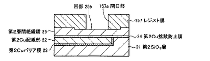
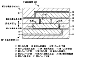
[半導体装置の構成]
図25及び26に、第3の実施形態に係る半導体装置の概略構成を示す。図25は、第3の実施形態に係る半導体装置の接合界面付近の概略断面図であり、図26は、各Cu接合部及び後述の第2Cuバリア層の界面層部間の配置関係を示す接合界面付近の概略上面図である。なお、図25及び26では、説明を簡略化するため、1つの接合界面付近の構成のみを示す。また、図25及び26に示す本実施形態の半導体装置3において、図3及び4に示す第1の実施形態の半導体装置1と同様の構成には、同じ符号を付して示す。
<3. Third Embodiment>
[Configuration of semiconductor device]
25 and 26 show a schematic configuration of the semiconductor device according to the third embodiment. FIG. 25 is a schematic cross-sectional view of the vicinity of the bonding interface of the semiconductor device according to the third embodiment, and FIG. 26 is a bonding showing the positional relationship between each Cu bonding portion and the interface layer portion of the second Cu barrier layer described later. It is a schematic top view of the interface vicinity. 25 and 26, only the configuration near one bonding interface is shown for the sake of simplicity. Further, in the semiconductor device 3 of the present embodiment shown in FIGS. 25 and 26, the same components as those of the semiconductor device 1 of the first embodiment shown in FIGS.
半導体装置3は、図25に示すように、第1半導体部材10(第1半導体部)と、第2半導体部材60(第2半導体部)とを備える。なお、本実施形態の半導体装置3における第1半導体部材10の構成は、上記第1の実施形態(図3)のそれと同様の構成であるので、ここでは、第1半導体部材10の説明は省略する。 As shown in FIG. 25, the semiconductor device 3 includes a first semiconductor member 10 (first semiconductor portion) and a second semiconductor member 60 (second semiconductor portion). In addition, since the structure of the 1st semiconductor member 10 in the semiconductor device 3 of this embodiment is the same structure as that of the said 1st Embodiment (FIG. 3), description of the 1st semiconductor member 10 is abbreviate | omitted here. To do.
第2半導体部材60は、第2半導体基板(不図示)、第2SiO2層21、第2Cu配線部22、第2Cuバリア膜23、第2Cu拡散防止膜24、第2層間絶縁膜25、第2Cu接合部26、及び、第2Cuバリア層61(バリアメタル層)を有する。
The second semiconductor member 60 includes a second semiconductor substrate (not shown), a second SiO 2 layer 21, a second
図25と図3との比較から明らかなように、本実施形態の第2半導体部材60は、第1の実施形態の第2半導体部材20において、界面Cuバリア膜28を省略し、かつ、第2Cuバリア層27の構成を変えたものとなる。それ以外の第2半導体部材60の構成は、上記第1の実施形態の第2半導体部材20の対応する構成と同様である。それゆえ、ここでは、第2Cuバリア層61の構成についてのみ説明する。
As apparent from the comparison between FIG. 25 and FIG. 3, the second semiconductor member 60 of the present embodiment omits the interface
第2Cuバリア層61は、図25に示すように、第2Cu接合部26を被覆するように設けられたバリア本体部61aと、該バリア本体部61aの接合界面Sj側の端部から接合界面Sjに沿って延在して形成された界面層部61b(界面バリア部)とを有する。
As shown in FIG. 25, the second
すなわち、本実施形態では、第1半導体部材10の第1Cu接合部16と、第2半導体部材60の第2層間絶縁膜25とが対向する接合界面Sjの領域に、第2Cuバリア層61の界面層部61bを配置する。そして、第2Cuバリア層61の界面層部61bが、第1Cu接合部16と第2層間絶縁膜25との対向領域を介して、Cu接合部から層間絶縁膜にCuが拡散することを防止する。それゆえ、本実施形態では、接合時に想定される最大の接合アライメントずれが発生しても、接合界面Sjに、第1Cu接合部16と第2層間絶縁膜25との接触領域が発生しないように、界面層部61bの接合界面Sjに沿う方向の幅を設定する。なお、第2Cuバリア層61は、上記第1の実施形態と同様に、例えば、Ti、Ta、Ru、又は、それらの窒化物等で形成される。
That is, in the present embodiment, the interface of the second
[半導体装置の製造手法]
次に、本実施形態の半導体装置3の製造手法を、図27〜34を参照しながら説明する。なお、図27〜33には、各工程で作製される半導体部材のCu接合部付近の概略断面を示し、図34には、第1半導体部材10と第2半導体部材60との接合処理の様子を示す。また、下記説明において、上記第1の実施形態の半導体装置の製造手法と同様の工程の説明では、上記第1の実施形態の工程の図面(図5〜17)を適宜参照する。さらに、本実施形態の第1半導体部材10の作製手法は、上記第1の実施形態のそれ(図5〜10)と同様であるので、ここでは、第1半導体部材10の作製手法の説明を省略し、第2半導体部材60の作製手法、及び、Cu−Cu接合手法について説明する。
[Semiconductor Device Manufacturing Method]
Next, a method for manufacturing the semiconductor device 3 of this embodiment will be described with reference to FIGS. 27 to 33 show a schematic cross section near the Cu bonding portion of the semiconductor member manufactured in each step, and FIG. 34 shows the bonding process between the first semiconductor member 10 and the second semiconductor member 60. Indicates. Further, in the following description, in the description of the process similar to the manufacturing method of the semiconductor device of the first embodiment, the drawings (FIGS. 5 to 17) of the process of the first embodiment are appropriately referred to. Furthermore, since the manufacturing method of the first semiconductor member 10 of the present embodiment is the same as that of the first embodiment (FIGS. 5 to 10), the manufacturing method of the first semiconductor member 10 will be described here. A description will be given of a manufacturing method of the second semiconductor member 60 and a Cu—Cu bonding method, which are omitted.
まず、本実施形態では、上記図5で説明した第1の実施形態の第1半導体部材10の作製工程と同様にして、第2SiO2層21上に、第2Cuバリア膜23、第2Cu配線部22、及び、第2Cu拡散防止膜24をこの順で形成する。次いで、上記図6で説明した第1の実施形態の第1半導体部材10の作製工程と同様にして、第2Cu拡散防止膜24上に、第2層間絶縁膜25を形成する。
First, in the present embodiment, a second
次いで、図27に示すように、第2層間絶縁膜25上にレジスト膜156を形成する。そして、フォトリソグラフィ技術を用いて、レジスト膜156に対してパターニング処理を施し、第2Cuバリア層61の形成領域のレジスト膜156を除去して開口部156aを形成する。これにより、レジスト膜156の開口部156aに第2層間絶縁膜25が露出する。
Next, as shown in FIG. 27, a resist film 156 is formed on the second
次いで、レジスト膜156が形成された半導体部材の開口部156a側の表面に対して、例えば従来既知のマグネトロン方式のエッチング装置を用いて、ドライエッチング処理を行う。これにより、レジスト膜156の開口部156aに露出した第2層間絶縁膜25の領域がエッチングされる。この際、第2層間絶縁膜25を、約10〜50nm程度、エッチングして除去する。この結果、図28に示すように、第2層間絶縁膜25の表面には、深さが約10〜50nm程度の凹部25bが形成される。
Next, a dry etching process is performed on the surface of the semiconductor member on which the resist film 156 is formed on the opening 156a side using, for example, a conventionally known magnetron etching apparatus. Thereby, the region of the second
その後、エッチング処理された面に対して、例えば酸素(O2)プラズマを用いたアッシング処理、及び、有機アミン系の薬液を用いた洗浄処理を施す。これにより、第2層間絶縁膜25上に残留したレジスト膜156、及び、上記エッチング処理で発生した残留付着物を除去する。
Thereafter, the etched surface is subjected to, for example, an ashing process using oxygen (O 2 ) plasma and a cleaning process using an organic amine chemical solution. Thus, the resist film 156 remaining on the second
次いで、図29に示すように、再度、第2Cu拡散防止膜24上にレジスト膜157を形成する。そして、フォトリソグラフィ技術を用いて、レジスト膜157に対してパターニング処理を施し、第2Cuバリア層61のバリア本体部61aの形成領域のレジスト膜157を除去して開口部157aを形成する。これにより、レジスト膜157の開口部157aに第2層間絶縁膜25の凹部25bの底部が露出する。
Next, as shown in FIG. 29, a resist film 157 is formed again on the second Cu
次いで、レジスト膜157が形成された半導体部材の開口部157a側の表面に対して、例えば従来既知のマグネトロン方式のエッチング装置を用いて、ドライエッチング処理を行う。これにより、レジスト膜157の開口部157aに露出した第2層間絶縁膜25の凹部25bの一部領域がエッチングされる。
Next, a dry etching process is performed on the surface of the semiconductor member on which the resist film 157 is formed on the opening 157a side using, for example, a conventionally known magnetron etching apparatus. Thereby, a partial region of the recess 25b of the second
このエッチング処理では、図30に示すように、開口部157aの領域の第2層間絶縁膜25及び第2Cu拡散防止膜24を除去し、第2層間絶縁膜25の開口部25aに第2Cu配線部22を露出させる。また、本実施形態では、第2層間絶縁膜25の開口部25aの開口径は、例えば、約1〜95μm程度とする。なお、このエッチング処理で除去されない第2層間絶縁膜25の凹部25bの領域は、第2Cuバリア層61の界面層部61bの形成領域となる。
In this etching process, as shown in FIG. 30, the second
その後、エッチング処理された面に対して、例えば酸素(O2)プラズマを用いたアッシング処理、及び、有機アミン系の薬液を用いた洗浄処理を施す。これにより、第2層間絶縁膜25上に残留したレジスト膜157、及び、上記エッチング処理で発生した残留付着物を除去する。
Thereafter, the etched surface is subjected to, for example, an ashing process using oxygen (O 2 ) plasma and a cleaning process using an organic amine chemical solution. As a result, the resist film 157 remaining on the second
次いで、図31に示すように、第2層間絶縁膜25上、及び、第2層間絶縁膜25の開口部25aに露出した第2Cu配線部22上に、Ti、Ta、Ru、又は、それらの窒化物からなる第2Cuバリア層61を形成する。具体的には、例えばRFスパッタリング法等の手法を用いて、Ar/N2雰囲気中で、厚さが約5〜50nmの第2Cuバリア層61を、第2層間絶縁膜25上、及び、第2Cu配線部22上に形成する。この処理により、第2層間絶縁膜25の開口部25aに露出した第2Cu配線部22上、及び、第2層間絶縁膜25の側面上に、バリア本体部61aが形成される。また、この処理により、第2層間絶縁膜25の凹部25b上に、界面層部61bが形成される。
Next, as shown in FIG. 31, Ti, Ta, Ru, or those on the second
次いで、図32に示すように、第2Cuバリア層61上に、例えばスパッタリング法及び電解メッキ法等の手法を用いて、Cu膜158を形成する。この処理により、第2層間絶縁膜25の開口部25aの領域にCu膜158が埋め込まれる。
Next, as shown in FIG. 32, a Cu film 158 is formed on the second
次いで、Cu膜158が形成された半導体部材を、例えばホットプレートやシンターアニール装置等の加熱装置を用いて、窒素雰囲気中又は真空中で、約100〜400℃で1〜60分程度加熱する。この加熱処理により、Cu膜158を引き締めて緻密な膜質のCu膜158を形成する。 Next, the semiconductor member on which the Cu film 158 is formed is heated at about 100 to 400 ° C. for about 1 to 60 minutes in a nitrogen atmosphere or in vacuum using a heating device such as a hot plate or a sinter annealing device. By this heat treatment, the Cu film 158 is tightened to form a dense Cu film 158.
そして、図33に示すように、Cu膜158及び第2Cuバリア層61の不要な部分を化学機械研磨(CMP)法により除去する。この際、第2層間絶縁膜25の凹部25b上に、界面層部61bが残るように、CMP法の処理条件を調整する。具体的には、第2層間絶縁膜25が表面に露出するまで、Cu膜158側の表面をCMP法で研磨する。本実施形態では、上述のようにして第2半導体部材60を作製する。
Then, as shown in FIG. 33, unnecessary portions of the Cu film 158 and the second
その後、上述のようにして作製された第2半導体部材60(図33)と、上記第1の実施形態と同様にして作製された第1半導体部材10(図10)とを、上記第1の実施形態と同様にして貼り合わせる。 Thereafter, the second semiconductor member 60 (FIG. 33) manufactured as described above and the first semiconductor member 10 (FIG. 10) manufactured in the same manner as the first embodiment are combined with the first semiconductor member 60 (FIG. 10). Bonding is performed in the same manner as in the embodiment.
具体的には、まず、第1半導体部材10の第1Cu接合部16側の表面、及び、第2半導体部材60の第2Cu接合部26側の表面に対して還元処理を施し、各Cu接合部の表面の酸化膜(酸化物)を除去して、各Cu接合部の表面に清浄なCuを露出させる。なお、この際、還元処理としては、例えば蟻酸等の薬液を用いたウェットエッチング処理、又は、例えばAr、NH3、H2等のプラズマを用いたドライエッチング処理が用いられる。
Specifically, first, reduction treatment is performed on the surface of the first semiconductor member 10 on the first
次いで、図34に示すように、第1半導体部材10の第1Cu接合部16側の表面と、第2半導体部材60の第2Cu接合部26側の表面とを接触させる(貼り合わせる)。そして、第1半導体部材10と第2半導体部材60とを貼り合わせた状態で、例えばホットプレートやRTA装置等の加熱装置を用いて貼り合わせ部材をアニールして、第1Cu接合部16と第2Cu接合部26とを接合する。具体的には、例えば、大気圧のN2雰囲気中、又は、真空中で約100〜400℃で5分〜2時間程度、貼り合わせ部材を加熱する。
Next, as shown in FIG. 34, the surface of the first semiconductor member 10 on the first
また、この接合処理により、第1Cu接合部16の接合界面Sj側の面領域のうち第2Cu接合部26と接合しない面領域を含む領域に第2Cuバリア層61の界面層部61bが配置される。より具体的には、図25に示すように、第1Cu接合部16と、第2層間絶縁膜25とが対向する接合界面Sjの領域を含む領域に第2Cuバリア層61の界面層部61bが配置される。
In addition, by this bonding process, the
本実施形態では、上述のようにして、Cu−Cu接合処理を行う。なお、上述した接合工程以外の半導体装置2の製造工程は、従来の例えば固体撮像装置等の半導体装置の製造手法(例えば特開2007−234725号公報参照)と同様にすることができる。
In the present embodiment, the Cu—Cu bonding process is performed as described above. Note that the manufacturing process of the
上述のように、本実施形態においても、上記第1の実施形態と同様に、第1半導体部材10の第1Cu接合部16と、第2半導体部材60の第2層間絶縁膜25とが対向する接合界面Sjの領域には、第2Cuバリア層61の界面層部61bが設けられる。それゆえ、本実施形態においても、第1の実施形態と同様の効果が得られる。
As described above, also in the present embodiment, the first
<4.各種変形例及び参考例>
次に、上述した各種実施形態の半導体装置の変形例を説明する。
<4. Various modifications and reference examples>
Next, modified examples of the semiconductor devices of the various embodiments described above will be described.
[変形例1]
上記第1の実施形態の半導体装置1(図3)では、第2半導体部材20の第2Cu配線部22上に、第2Cu拡散防止膜24、第2層間絶縁膜25、及び、界面Cuバリア膜28を設ける構成例を説明したが、本開示はこれに限定されない。例えば、第2Cu配線部22上に、界面Cuバリア膜のみを設ける構成にしてもよい。
[Modification 1]
In the semiconductor device 1 (FIG. 3) of the first embodiment, the second Cu
図35に、その一例(変形例1)を示す。図35は、変形例1の半導体装置4の接合界面Sj付近の概略構成断面図である。なお、図35に示すこの例の半導体装置4において、図3に示す第1の実施形態の半導体装置1と同様の構成には、同じ符号を付して示す。 FIG. 35 shows an example (Modification 1). FIG. 35 is a schematic cross-sectional view of the vicinity of the junction interface Sj of the semiconductor device 4 of Modification 1. In the semiconductor device 4 of this example shown in FIG. 35, the same components as those of the semiconductor device 1 of the first embodiment shown in FIG.
この例の半導体装置4は、図35に示すように、第1半導体部材10と、第2半導体部材70とを備える。なお、この例の半導体装置4における第1半導体部材10の構成は、上記第1の実施形態(図3)のそれと同様の構成であるので、ここでは、第1半導体部材10の説明は省略する。 The semiconductor device 4 of this example includes a first semiconductor member 10 and a second semiconductor member 70 as shown in FIG. In addition, since the structure of the 1st semiconductor member 10 in the semiconductor device 4 of this example is the structure similar to that of the said 1st Embodiment (FIG. 3), description of the 1st semiconductor member 10 is abbreviate | omitted here. .
第2半導体部材70は、第2半導体基板(不図示)、第2SiO2層21、第2Cu配線部22、第2Cuバリア膜23、界面Cuバリア膜71(界面バリア膜、界面バリア部)、第2Cu接合部26、及び、第2Cuバリア層27を有する。なお、この例の第2半導体部材70において、界面Cuバリア膜71以外の構成は、上記第1の実施形態の第2半導体部材20の対応する構成と同様の構成である。
The second semiconductor member 70 includes a second semiconductor substrate (not shown), a second SiO 2 layer 21, a second
界面Cuバリア膜71(Cu拡散防止膜)は、第2SiO2層21、第2Cu配線部22及び第2Cuバリア膜23上に設けられ、かつ、第2Cuバリア層27の側部を覆うように設けられる。それゆえ、この例では、界面Cuバリア膜71は、Cu接合部から層間絶縁膜へのCuの拡散を防止するだけでなく、上記第1の実施形態の第2半導体部材20の第2Cu拡散防止膜24及び第2層間絶縁膜25と同様の役割も兼ねる。
The interfacial Cu barrier film 71 (Cu diffusion preventing film) is provided on the second SiO 2 layer 21, the second
なお、界面Cuバリア膜71は、上記第1の実施形態の界面Cuバリア膜28と同様に、例えば、SiN、SiON、SiCN、有機系樹脂等の材料で形成することができる。
The interface Cu barrier film 71 can be formed of a material such as SiN, SiON, SiCN, or organic resin, for example, as with the interface
この例の第2半導体部材70は、例えば、次のようにして作製することができる。まず、上記図5で説明した第1の実施形態の第1半導体部材10の作製工程と同様にして、第2SiO2層21上に、第2Cuバリア膜23、及び、第2Cu配線部22をこの順で形成する。次いで、第2SiO2層21、第2Cu配線部22及び第2Cuバリア膜23上に、厚さが約5〜500nmの界面Cuバリア膜71を形成する。
The second semiconductor member 70 of this example can be manufactured as follows, for example. First, the second
次いで、図36に示すように、界面Cuバリア膜71上にレジスト膜159を形成する。その後、フォトリソグラフィ技術を用いて、レジスト膜159に対してパターニング処理を施し、第2Cu接合部26の形成領域のレジスト膜159を除去して開口部159aを形成する。これにより、レジスト膜159の開口部159aに界面Cuバリア膜71が露出する。その後は、上記図13〜16で説明した上記第1の実施形態の第2半導体部材20の作製工程と同様にして、この例の第2半導体部材70を作製する。
Next, as shown in FIG. 36, a resist film 159 is formed on the interface Cu barrier film 71. Thereafter, a patterning process is performed on the resist film 159 by using a photolithography technique, and the resist film 159 in the formation region of the second
この例の構成では、第1Cu接合部16の接合界面Sj側の面領域のうち第2Cu接合部26と接合しない面領域は、界面Cuバリア膜71と接触した状態となる。それゆえ、この例の構成においても、各Cu接合部のCuが外部の酸化膜に拡散することがないので、第1の実施形態と同様の効果が得られる。
In the configuration of this example, the surface region not bonded to the second
[変形例2]
上記第2の実施形態では、第1半導体部材30及び第2半導体部材40のいずれにも、Cuシード層を設ける例(図18参照)を説明したが、本開示はこれに限定されない。少なくとも、Cu接合部の接合側の表面面積が大きい方の半導体部材にCuシード層を設ければよい。例えば、図18に示す半導体装置2では、第1半導体部材30の第1Cu接合部16と、第1Cuバリア層17との間のみにCuシード層を設ければよい。
[Modification 2]
In the second embodiment, the example in which the Cu seed layer is provided in both the first semiconductor member 30 and the second semiconductor member 40 (see FIG. 18) has been described, but the present disclosure is not limited thereto. A Cu seed layer may be provided at least on the semiconductor member having a larger surface area on the bonding side of the Cu bonding portion. For example, in the
この場合にも、接合時のアニール処理により、第1半導体部材30のCuシード層中の例えばMn、Mg、Ti、Al等の金属材料が、接合界面Sjを挟んで対向する第2半導体部材40の第2層間絶縁膜25中の酸素と反応する。その結果、この例においても、上記第2の実施形態と同様に、第1半導体部材30の第1Cu接合部16と、第2半導体部材40の第2層間絶縁膜25とが対向する接合界面Sjの領域に界面バリア膜が形成され、第1の実施形態と同様の効果が得られる。
Also in this case, the second semiconductor member 40 facing the metal material such as Mn, Mg, Ti, Al, etc. in the Cu seed layer of the first semiconductor member 30 with the bonding interface Sj sandwiched by the annealing process at the time of bonding. It reacts with oxygen in the second
[変形例3]
上記第3の実施形態では、第2半導体部材60において、第2Cuバリア層61の界面層部61bを第2層間絶縁膜25の接合側表面に埋め込むように形成する例を説明したが、本開示はこれに限定されない。例えば、界面層部61bを、第2層間絶縁膜25の接合側表面上に設ける構成にしてもよい。
[Modification 3]
In the third embodiment, the example in which the
図37に、その一例(変形例3)を示す。図37は、変形例3の半導体装置5の接合界面Sj付近の概略構成断面図である。また、図37に示すこの例の半導体装置5において、図25に示す第3の実施形態の半導体装置3と同様の構成には、同じ符号を付して示す。 FIG. 37 shows an example (Modification 3). FIG. 37 is a schematic cross-sectional view of the vicinity of the junction interface Sj of the semiconductor device 5 of Modification 3. In addition, in the semiconductor device 5 of this example shown in FIG. 37, the same components as those of the semiconductor device 3 of the third embodiment shown in FIG.
この例の半導体装置5は、図37に示すように、第1半導体部材10と、第2半導体部材80とを備える。なお、この例の半導体装置5における第1半導体部材10の構成は、上記第3の実施形態(図25)のそれと同様の構成であるので、ここでは、第1半導体部材10の説明は省略する。 The semiconductor device 5 of this example includes a first semiconductor member 10 and a second semiconductor member 80 as shown in FIG. In addition, since the structure of the 1st semiconductor member 10 in the semiconductor device 5 of this example is the same structure as that of the said 3rd Embodiment (FIG. 25), description of the 1st semiconductor member 10 is abbreviate | omitted here. .
第2半導体部材80は、第2半導体基板(不図示)、第2SiO2層21、第2Cu配線部22、第2Cuバリア膜23、第2Cu拡散防止膜24、第2層間絶縁膜81、第2Cu接合部26、第2Cuバリア層61、及び、界面Cuバリア膜82を有する。
The second semiconductor member 80 includes a second semiconductor substrate (not shown), a second SiO 2 layer 21, a second
なお、この例の第2半導体部材80において、第2半導体基板(不図示)、第2SiO2層21、第2Cu配線部22、第2Cuバリア膜23、及び、第2Cu拡散防止膜24の構成は、上記第3の実施形態の第2半導体部材60の対応する構成と同様の構成である。また、この例の第2Cu接合部26、及び、第2Cuバリア層61の構成は、上記第3の実施形態の第2半導体部材60の対応する構成と同様の構成である。
In the second semiconductor member 80 of this example, the configuration of the second semiconductor substrate (not shown), the second SiO 2 layer 21, the second
この例では、第2Cuバリア層61の界面層部61bは、第2層間絶縁膜81の接合側表面上に設けられる。それゆえ、第2層間絶縁膜81の表面には、上記第3の実施形態のように凹部25bは形成されない。
In this example, the
さらに、この例では、界面Cuバリア膜82が、第2層間絶縁膜81の表面上に形成され、かつ、第2Cuバリア層61の界面層部61bの側部(側面)を覆うように設けられる。また、この際、界面Cuバリア膜82の膜厚と界面層部61bの膜厚とを略同じにして、界面Cuバリア膜82の接合界面Sj側の表面と、界面層部61bの接合界面Sj側の表面とが略面一となるようにする。なお、界面Cuバリア膜82は、上記第1の実施形態の界面Cuバリア膜28と同様に、例えば、SiN、SiON、SiCN、有機系樹脂等の材料で形成することができる。
Furthermore, in this example, the interface
この例では、接合界面Sjにおいて、第1Cu接合部16と第2Cu接合部26との接合領域以外の領域では、第1Cu接合部16は、第2Cuバリア層61の界面層部61b及び/又は界面Cuバリア膜82と接触した状態となる。それゆえ、この例の構成においても、各Cu接合部のCuが層間絶縁膜に拡散することを防止することができるので、第1の実施形態と同様の効果が得られる。
In this example, in the bonding interface Sj, in the region other than the bonding region between the first
なお、この例では、界面Cuバリア膜82を設けない構成にしてもよい。この場合、第2Cuバリア層61の界面層部61bの側部の周囲には空隙が形成されるが、この空隙により、各Cu接合部のCuが層間絶縁膜に拡散することを防止することができるので、第1の実施形態と同様の効果が得られる。ただし、接合界面Sjの接合強度の観点では、図37に示すように、界面層部61bの側部を覆うように界面Cuバリア膜82を設けることが好ましい。
In this example, the interface
[変形例4]
上記各種実施形態及び各種変形例では、各接合部の電極膜をCu膜で構成する例を説明したが、本開示はこれに限定されない。接合部を、例えば、Al、W、Ti、TiN、Ta、TaN、Ru等で形成された金属膜、又は、これらの積層膜で構成していてもよい。
[Modification 4]
In the above-described various embodiments and various modifications, the example in which the electrode film of each joint portion is formed of a Cu film has been described, but the present disclosure is not limited thereto. For example, the bonding portion may be formed of a metal film formed of Al, W, Ti, TiN, Ta, TaN, Ru, or the like, or a stacked film thereof.
例えば、上記第1の実施形態において、接合部の電極材料としてAl(アルミニウム)を用いることができる。この場合には、界面Cuバリア膜28を、上記第1の実施形態と同様に、例えば、SiN、SiON、SiCN、樹脂等の材料で形成することができる。また、この場合、Al接合部を被覆するメタルバリア層は、Al接合部側からTi膜及びTiN膜をこの順で積層した多層膜(Ti/TiN積層膜)で構成することが好ましい。
For example, in the first embodiment, Al (aluminum) can be used as the electrode material of the joint. In this case, the interface
また、例えば、上記第2の実施形態の構成においても、接合部の電極材料としてAlを用いることができる。ただし、この場合には、Alは酸素と反応し易い材料であるので、界面バリア膜を生成するためのシード層(Cuシード層)を設ける必要がない。 Further, for example, in the configuration of the second embodiment, Al can be used as the electrode material of the joint portion. However, in this case, since Al is a material that easily reacts with oxygen, it is not necessary to provide a seed layer (Cu seed layer) for generating an interface barrier film.
ここで、図38に、上記第2の実施形態の構成において、接合部をAlで形成した場合の半導体装置の接合界面Sj付近の概略構成断面を示す。なお、図38では、説明を簡略化するため、Al接合部付近の構成のみを示し、配線部の構成は省略する。また、図38に示す半導体装置6において、図18に示す第2の実施形態の半導体装置2と同様の構成には、同じ符号を付して示す。
Here, FIG. 38 shows a schematic configuration cross section in the vicinity of the junction interface Sj of the semiconductor device when the junction is formed of Al in the configuration of the second embodiment. In FIG. 38, only the configuration near the Al junction is shown, and the configuration of the wiring portion is omitted for the sake of simplicity. In addition, in the semiconductor device 6 shown in FIG. 38, the same components as those in the
この例の半導体装置6は、図38に示すように、第1半導体部材91と、第2半導体部材92と、界面バリア膜97とを備える。第1半導体部材91は、第1層間絶縁膜15と、その接合側表面に埋め込むようにして形成された第1Al接合部93と、第1層間絶縁膜15及び第1Al接合部93間に設けられた第1バリアメタル層94とを有する。また、第2半導体部材92は、第2層間絶縁膜25と、その接合側表面に埋め込むようにして形成された第2Al接合部95と、第2層間絶縁膜25及び第2Al接合部95間に設けられた第2バリアメタル層96とを有する。
As shown in FIG. 38, the semiconductor device 6 of this example includes a first semiconductor member 91, a second semiconductor member 92, and an interface barrier film 97. The first semiconductor member 91 is provided between the first
そして、図38に示す例においても、第1半導体部材91と第2半導体部材92との接合時に行うアニール処理により、第1Al接合部93内のAlの一部が、接合界面Sjを挟んで対向する第2半導体部材92の第2層間絶縁膜25中の酸素と反応する。その結果、第1Al接合部93と、第2層間絶縁膜25とが対向する接合界面Sjの領域には、界面バリア膜97が形成される。それゆえ、この構成例においても、第1の実施形態と同様に、第1半導体部材91及び第2半導体部材92間の接合強度を増大させることができ、より信頼性の高い接合界面を有する半導体装置6を得ることができる。
Also in the example shown in FIG. 38, a part of Al in the first Al
さらに、例えば、上記第1の実施形態において、接合部の電極材料として例えばW(タングステン)を用いることができる。この場合には、界面Cuバリア膜28を、上記第1の実施形態と同様に、例えば、SiN、SiON、SiCN、樹脂等の材料で形成することができる。また、この場合、W接合部を被覆するメタルバリア層は、W接合部側からTi膜及びTiN膜をこの順で積層した多層膜(Ti/TiN積層膜)で構成することが好ましい。なお、Wは酸素と反応し難い(界面バリア膜を自己生成し難い)金属材料であるので、上記第2の実施形態の構成の接合部にWを用いることは難しい。
Further, for example, in the first embodiment, for example, W (tungsten) can be used as the electrode material of the bonding portion. In this case, the interface
[変形例5]
上記各種実施形態及び各種変形例では、信号が供給される金属膜同士を、接合界面Sjで接合する例を説明したが、本開示はこれに限定されない。信号が供給されない金属膜同士を接合界面Sjで接合する場合も、上記各種実施形態及び各種変形例で説明したCu−Cu接合技術を適用することができる。
[Modification 5]
In the various embodiments and various modifications described above, the example in which the metal films to which signals are supplied is bonded at the bonding interface Sj has been described, but the present disclosure is not limited thereto. Even when the metal films to which no signal is supplied are bonded at the bonding interface Sj, the Cu-Cu bonding technique described in the various embodiments and various modifications can be applied.
例えば、ダミー電極同士を接合する場合にも、上記各種実施形態及び各種変形例で説明したCu−Cu接合技術を適用することができる。また、例えば、固体撮像素子において、センサ部とロジック回路部との間で金属膜同士を接合して、遮光膜を形成する場合にも、上記各種実施形態及び各種変形例で説明したCu−Cu接合技術を適用することができる。 For example, also when joining dummy electrodes, the Cu-Cu joining technique demonstrated in the said various embodiment and various modifications is applicable. In addition, for example, in a solid-state imaging device, when a light shielding film is formed by bonding metal films between a sensor unit and a logic circuit unit, the Cu—Cu described in the above various embodiments and various modifications. Joining techniques can be applied.
[参考例1]
上記第2の実施形態では、第1Cu接合部16の接合界面Sj側表面の寸法(表面面積)と、第2Cu接合部26のそれとが異なる例を説明した。しかしながら、上記第2の実施形態で説明したCu−Cu接合技術は、第1Cu接合部の接合界面Sj側の表面形状及び寸法と、第2Cu接合部のそれらとが同じである半導体装置にも適用可能である。
[Reference Example 1]
In the second embodiment, the example in which the dimension (surface area) of the surface of the first
図39に、その一例(参考例1)を示す。なお、図39は、この例の半導体装置100の接合界面Sj付近の概略構成断面図である。また、図39に示すこの例の半導体装置100において、図18に示す第2の実施形態の半導体装置2と同様の構成には、同じ符号を付して示す。
FIG. 39 shows an example (Reference Example 1). FIG. 39 is a schematic cross-sectional view of the vicinity of the junction interface Sj of the semiconductor device 100 of this example. In addition, in the semiconductor device 100 of this example shown in FIG. 39, the same components as those of the
この例の半導体装置100は、図39に示すように、第1半導体部材101と、第2半導体部材40と、界面Cuバリア膜105とを備える。なお、この例の半導体装置100における第2半導体部材40の構成は、上記第2の実施形態(図18)のそれと同様の構成であるので、ここでは、第2半導体部材40の説明は省略する。
As shown in FIG. 39, the semiconductor device 100 of this example includes a first semiconductor member 101, a second semiconductor member 40, and an interface
第1半導体部材101は、第1半導体基板(不図示)、第1SiO2層11、第1Cu配線部12、第1Cuバリア膜13、第1Cu拡散防止膜14、第1層間絶縁膜15、第1Cu接合部102、第1Cuバリア層103、及び、第1Cuシード層104を有する。
The first semiconductor member 101 includes a first semiconductor substrate (not shown), a first SiO 2 layer 11, a first
なお、この例では、第1Cu接合部102の接合界面Sj側の表面形状及び寸法を、第2Cu接合部26のそれらと同じにする。それ以外の第1半導体部材101の構成は、上記第2の実施形態の第1半導体部材30の対応する構成と同様の構成である。
In this example, the surface shape and dimensions of the first
そして、この例においても、上記第2の実施形態と同様に、第1半導体部材101の第1Cu接合部102側の表面と、第2半導体部材40の第2Cu接合部26側の表面とを接合することにより、半導体装置100が作製される。この際、両Cu接合部間に、接合アライメントずれが発生すると、接合時のアニール処理により、各Cuシード層中の例えばMn、Mg、Ti、Al等の金属材料が接合界面Sjを挟んで対向する層間絶縁膜の酸素と選択的に反応する。この結果、図39に示すように、第1Cu接合部102と第2層間絶縁膜25とが対向する接合界面Sjの領域、及び、第2Cu接合部26と第1層間絶縁膜15とが対向する接合界面Sjの領域にそれぞれ、界面Cuバリア膜105が形成される。
Also in this example, similarly to the second embodiment, the surface of the first semiconductor member 101 on the first
上述のように、この例の半導体装置100においても、一方の半導体部材のCu接合部と、他方の半導体部材の層間絶縁膜とが対向する接合界面Sjの領域には、界面Cuバリア膜105が設けられる。それゆえ、この例においても、第2の実施形態と同様の効果が得られる。
As described above, also in the semiconductor device 100 of this example, the interface
[参考例2]
上記参考例1では、第1Cu接合部の接合界面Sj側の表面形状及び寸法と、第2Cu接合部のそれらとが同じである半導体装置に、上記第2の実施形態で説明したCu−Cu接合技術を適用する例を説明した。ここでは、参考例1の半導体装置100にさらに、上記第1の実施形態で説明したCu−Cu接合技術を組み合わせた構成例を説明する。
[Reference Example 2]
In the reference example 1, the Cu—Cu bonding described in the second embodiment is applied to the semiconductor device in which the surface shape and dimensions on the bonding interface Sj side of the first Cu bonding portion are the same as those of the second Cu bonding portion. An example of applying the technology has been described. Here, a configuration example is described in which the semiconductor device 100 of Reference Example 1 is further combined with the Cu—Cu bonding technique described in the first embodiment.
図40に、その一例(参考例2)を示す。なお、図40は、この例の半導体装置110の接合界面Sj付近の概略構成断面図である。また、図40に示すこの例の半導体装置110において、図39に示す参考例1の半導体装置100と同様の構成には、同じ符号を付して示す。 FIG. 40 shows an example (Reference Example 2). FIG. 40 is a schematic sectional view of the vicinity of the junction interface Sj of the semiconductor device 110 of this example. In addition, in the semiconductor device 110 of this example shown in FIG. 40, the same reference numerals are given to the same components as those of the semiconductor device 100 of Reference Example 1 shown in FIG.
この例の半導体装置110は、図40に示すように、第1半導体部材101と、第2半導体部材120と、第1界面Cuバリア膜121とを備える。なお、この例の半導体装置110における第1半導体部材101の構成は、上記参考例1(図39)のそれと同様の構成であるので、ここでは、第1半導体部材101の説明は省略する。
As shown in FIG. 40, the semiconductor device 110 of this example includes a first semiconductor member 101, a second semiconductor member 120, and a first interface
第2半導体部材120は、第2半導体基板(不図示)、第2SiO2層21、第2Cu配線部22、第2Cuバリア膜23、第2Cu拡散防止膜24、第2層間絶縁膜25、第2Cu接合部26、第2Cuバリア層27、及び、第2Cuシード層41を有する。さらに、第2半導体部材120は、第2界面Cuバリア膜122を有する。
The second semiconductor member 120 includes a second semiconductor substrate (not shown), a second SiO 2 layer 21, a second
図40と図39との比較から明らかなように、この例の第2半導体部材120は、上記参考例1の第2半導体部材40において、第2層間絶縁膜25上に第2界面Cuバリア膜122を設けた構成である。また、この例では、第2Cu接合部26の接合界面Sj側の表面と、第2界面Cuバリア膜122の表面とが略面一となるように、第2界面Cuバリア膜122を形成する。なお、第2界面Cuバリア膜122以外の第2半導体部材120の構成は、上記参考例1の第2半導体部材40の対応する構成と同様である。
As apparent from the comparison between FIG. 40 and FIG. 39, the second semiconductor member 120 of this example is the same as the second semiconductor member 40 of Reference Example 1 except that the second interface Cu barrier film is formed on the second
また、第2界面Cuバリア膜122は、上記第1の実施形態の界面Cuバリア膜28と同様に、例えば、SiN、SiON、SiCN、有機系樹脂等の材料で形成することができる。ただし、Cu膜との密着性という観点では、特に、第2界面Cuバリア膜122をSiNで形成することが好ましい。
The second interface Cu barrier film 122 can be formed of a material such as SiN, SiON, SiCN, or organic resin, for example, as with the interface
そして、この例においても、上記第2の実施形態と同様に、第1半導体部材101の第1Cu接合部102側の表面と、第2半導体部材120の第2Cu接合部26側の表面とを接合することにより、半導体装置110が作製される。この際、両Cu接合部間に、接合アライメントずれが発生すると、接合時のアニール処理により、各Cuシード層中の例えばMn、Mg、Ti、Al等の金属材料が接合界面Sjを挟んで対向する層間絶縁膜の酸素と選択的に反応する。この結果、一方の半導体部材のCu接合部と、他方の半導体部材の層間絶縁膜とが対向する接合界面Sj領域に、第1界面Cuバリア膜121が形成される。
Also in this example, similarly to the second embodiment, the surface of the first semiconductor member 101 on the first
ただし、この例では、上述のように、第2半導体部材120の接合界面Sjの表面に第2界面Cuバリア膜122を設ける。それゆえ、この例では、第1Cu接合部102と第2層間絶縁膜25とが対向する接合界面Sjの領域、及び、第2Cu接合部26と第1層間絶縁膜15とが対向する接合界面Sjの領域の一方に、第1界面Cuバリア膜121が形成される。また、第1Cu接合部102と第2層間絶縁膜25とが対向する接合界面Sjの領域、及び、第2Cu接合部26と第1層間絶縁膜15とが対向する接合界面Sjの領域の他方に、第2界面Cuバリア膜122が配置される。図40に示す例では、前者の接合界面Sjの領域に、第2界面Cuバリア膜122が設けられ、後者の接合界面Sjの領域に、第1界面Cuバリア膜121が設けられる。
However, in this example, as described above, the second interface Cu barrier film 122 is provided on the surface of the bonding interface Sj of the second semiconductor member 120. Therefore, in this example, the region of the bonding interface Sj where the first
上述のように、この例の半導体装置110においても、一方の半導体部材のCu接合部と、他方の半導体部材の層間絶縁膜とが対向する接合界面Sjの領域には、第1界面Cuバリア膜121又は第2界面Cuバリア膜122が設けられる。それゆえ、この例においても、第1及び第2の実施形態と同様の効果が得られる。 As described above, also in the semiconductor device 110 of this example, the first interface Cu barrier film is formed in the region of the bonding interface Sj where the Cu bonding portion of one semiconductor member and the interlayer insulating film of the other semiconductor member face each other. 121 or the second interface Cu barrier film 122 is provided. Therefore, also in this example, the same effect as the first and second embodiments can be obtained.
<5.第4の実施形態>
通常、Cu接合部の面積が互いに異なる第1半導体部材及び第2半導体部材を貼り合わせてCu−Cu接合を行う場合、一方の半導体部材のCu接合部と、他方の半導体部材の層間絶縁膜とが接触する。図41に、その接合例における接合界面付近の概略断面図を示す。なお、図41に示す半導体装置650において、図3に示す第1の実施形態の半導体装置1と同様の構成には、同じ符号を付して示す。
<5. Fourth Embodiment>
Usually, when Cu-Cu bonding is performed by bonding the first semiconductor member and the second semiconductor member having different areas of the Cu bonding portion, the Cu bonding portion of one semiconductor member and the interlayer insulating film of the other semiconductor member Touch. FIG. 41 shows a schematic cross-sectional view in the vicinity of the bonding interface in the bonding example. In the semiconductor device 650 shown in FIG. 41, the same components as those in the semiconductor device 1 of the first embodiment shown in FIG.
この場合、図41に示すように、第2Cu接合部26より面積の大きな第1Cu接合部16から第2層間絶縁膜25にCuが拡散して(図41中の点線矢印)、接合界面Sjにおける電気特性が劣化し、Cu接合部及び半導体装置650の信頼性が損なわれる。それに対して、上記各種実施形態では、第1Cu接合部16と第2層間絶縁膜25との接合界面に界面バリア膜を形成して、第1Cu接合部16から第2層間絶縁膜25へのCuの拡散を防止することができ、上記問題を解消することができる。
In this case, as shown in FIG. 41, Cu diffuses from the
また、上述した接合界面におけるCuの拡散を防止する別の手法としては、第1半導体部材及び第2半導体部材の少なくとも一方の接合界面側の層間絶縁膜の表面をCu接合部の接合側表面より後退させた状態で、両者を貼り合わせる手法も考えられる。すなわち、第1半導体部材及び第2半導体部材の少なくとも一方のCu接合部を接合界面側に突出させた状態で、両者を貼り合わせる手法も考えられる。 Further, as another method for preventing the diffusion of Cu at the bonding interface described above, the surface of the interlayer insulating film on the bonding interface side of at least one of the first semiconductor member and the second semiconductor member is made to be more than the bonding side surface of the Cu bonding portion. A method is also conceivable in which the two are bonded together in the retracted state. That is, a method is also conceivable in which both of the first semiconductor member and the second semiconductor member are bonded together in a state in which at least one Cu bonding portion protrudes toward the bonding interface.
図42に、第1半導体部材及び第2半導体部材の両方のCu接合部を接合界面側に突出させた状態で両者を貼り合わせた場合の、接合界面付近の概略断面図を示す。なお、図42に示す半導体装置660において、図3に示す第1の実施形態の半導体装置1と同様の構成には、同じ符号を付して示す。 FIG. 42 is a schematic cross-sectional view of the vicinity of the bonding interface when both of the first semiconductor member and the second semiconductor member are bonded together in a state where the Cu bonding portions protrude toward the bonding interface. In the semiconductor device 660 shown in FIG. 42, the same components as those in the semiconductor device 1 of the first embodiment shown in FIG.
この場合には、第1半導体部材661及び第2半導体部材662の接合界面Sj(第1層間絶縁膜663と第2層間絶縁膜664との間)に隙間ができる。これにより、第2層間絶縁膜664と第1Cu接合部16との間には空隙が形成され、第1Cu接合部16から第2層間絶縁膜664へのCuの拡散が防止される。しかしながら、この場合には、図42に示すように、接合界面Sjの隙間に外気(白抜き矢印)が浸入して第1Cu接合部16の表面を汚染し、これにより、接合界面Sjにおける電気特性が劣化し、Cu接合部及び半導体装置の信頼性が損なわれる。
In this case, a gap is formed at the junction interface Sj (between the first
そこで、第4の実施形態では、第2層間絶縁膜と第1Cu接合部との間に空隙を形成した構成を有する半導体装置において、上述した外気の影響を防止できる構成例を説明する。 Therefore, in the fourth embodiment, a configuration example that can prevent the above-described influence of the outside air in a semiconductor device having a configuration in which a gap is formed between the second interlayer insulating film and the first Cu junction will be described.
[半導体装置の構成]
図43及び44に、第4の実施形態に係る半導体装置の概略構成を示す。図43は、第4の実施形態に係る半導体装置の接合界面付近の概略断面図であり、図44は、各Cu接合部と接合界面に画成される空隙との配置関係を示す接合界面付近の概略上面図である。なお、図43及び44では、説明を簡略化するため、1つの接合界面付近の構成のみを示す。また、図43に示す本実施形態の半導体装置130において、図3に示す第1の実施形態の半導体装置1と同様の構成には、同じ符号を付して示す。
[Configuration of semiconductor device]
43 and 44 show a schematic configuration of the semiconductor device according to the fourth embodiment. FIG. 43 is a schematic cross-sectional view of the vicinity of the bonding interface of the semiconductor device according to the fourth embodiment, and FIG. 44 is the vicinity of the bonding interface showing the positional relationship between each Cu bonding portion and the void defined in the bonding interface. FIG. 43 and 44, only the configuration near one junction interface is shown for the sake of simplicity. Also, in the semiconductor device 130 of the present embodiment shown in FIG. 43, the same reference numerals are given to the same configurations as those of the semiconductor device 1 of the first embodiment shown in FIG.
半導体装置130は、図43に示すように、第1半導体部材131(第1半導体部)と、第2半導体部材132(第2半導体部)とを備える。 As shown in FIG. 43, the semiconductor device 130 includes a first semiconductor member 131 (first semiconductor portion) and a second semiconductor member 132 (second semiconductor portion).
第1半導体部材131は、第1半導体基板(不図示)、第1SiO2層11、第1Cu配線部12、第1Cuバリア膜13、第1Cu拡散防止膜14、第1層間絶縁膜15、第1Cu接合部133、及び、第1Cuバリア層17を有する。
The first semiconductor member 131 includes a first semiconductor substrate (not shown), a first SiO 2 layer 11, a first
図43と図3との比較から明らかなように、本実施形態の第1半導体部材131は、第1の実施形態の第1半導体部材10の接合界面Sj側の表面領域において、第2層間絶縁膜25と対向する第1Cu接合部16の表面領域に凹部を設けた構成となる。それ以外の第1半導体部材131の構成は、上記第1の実施形態の第1半導体部材10の対応する構成と同様である。
As is clear from comparison between FIG. 43 and FIG. 3, the first semiconductor member 131 of the present embodiment has a second interlayer insulation in the surface region on the bonding interface Sj side of the first semiconductor member 10 of the first embodiment. The surface area of the first
第2半導体部材132は、第2半導体基板(不図示)、第2SiO2層21、第2Cu配線部22、第2Cuバリア膜23、第2Cu拡散防止膜24、第2層間絶縁膜25、及び、第2Cu接合部26を有する。
The
図43と図3との比較から明らかなように、本実施形態の第2半導体部材132は、第1の実施形態の第2半導体部材20において、界面Cuバリア膜28を省略した構成となる。それ以外の第2半導体部材132の構成は、上記第1の実施形態の第2半導体部材20の対応する構成と同様である。
As is clear from a comparison between FIG. 43 and FIG. 3, the
本実施形態の半導体装置130では、図43に示すように、第1半導体部材131の接合界面Sj側の表面領域において、第2半導体部材132の第2層間絶縁膜25と対向する第1Cu接合部133の表面領域に凹部134を設ける。これにより、第1半導体部材131の第1Cu接合部133と、第2半導体部材132の第2層間絶縁膜25とが対向する接合界面Sjの領域に空隙が形成され、第1Cu接合部133が、第2層間絶縁膜25と直接接触しない構造を形成することができる。
In the semiconductor device 130 of the present embodiment, as shown in FIG. 43, in the surface region on the bonding interface Sj side of the first semiconductor member 131, the first Cu junction portion facing the second
すなわち、本実施形態の半導体装置130では、第1Cu接合部133の凹部134と、凹部134と対向する第2半導体部材132の接合界面Sj側の表面領域部(面領域部)とにより界面バリア部が構成される。また、本実施形態では、図43に示すように、第1Cu接合部133の凹部134と第2層間絶縁膜25の接合界面Sj側の表面とにより画成された空隙が、その周辺の各種膜により密封された状態になる。
That is, in the semiconductor device 130 of the present embodiment, the interface barrier portion is formed by the
[半導体装置の製造手法]
次に、本実施形態の半導体装置130の製造手法を、図45〜48を参照しながら説明する。なお、図45及び46には、各工程で作製される半導体部材のCu接合部付近の概略断面を示し、図47及び48には、第1半導体部材131と第2半導体部材132との接合処理の様子を示す。
[Semiconductor Device Manufacturing Method]
Next, a method for manufacturing the semiconductor device 130 of this embodiment will be described with reference to FIGS. 45 and 46 show schematic cross sections in the vicinity of the Cu bonding portion of the semiconductor member manufactured in each step, and FIGS. 47 and 48 show the bonding process between the first semiconductor member 131 and the
まず、本実施形態では、図5〜10で説明した第1の実施形態の第1半導体部材10の作製工程と同様にして、第1半導体部材131を作製する(図45の状態)。 First, in the present embodiment, the first semiconductor member 131 is manufactured in the same manner as the manufacturing process of the first semiconductor member 10 of the first embodiment described with reference to FIGS.
また、本実施形態では、図5〜10で説明した第1の実施形態の第1半導体部材10の作製工程と同様にして、第2半導体部材132を作製する(図46の状態)。ただし、この際、第2層間絶縁膜25に、第2Cu接合部26及び第2Cuバリア層27の形成領域に対応する開口部を形成する工程(図7の工程に対応)では、開口部の開口径を約1〜95μm程度とする。
Moreover, in this embodiment, the
次いで、第1半導体部材131の第1Cu接合部133側の表面、及び、第2半導体部材132の第2Cu接合部26側の表面に対して還元処理を施し、各Cu接合部の表面の酸化膜(酸化物)を除去して、各Cu接合部の表面に清浄なCuを露出させる。なお、この際、還元処理としては、例えば蟻酸等の薬液を用いたウェットエッチング処理、又は、例えばAr、NH3、H2等のプラズマを用いたドライエッチング処理が用いられる。
Next, a reduction treatment is performed on the surface of the first semiconductor member 131 on the first Cu bonding portion 133 side and the surface of the
次いで、図47に示すように、第1半導体部材131の第1Cu接合部133側の表面と、第2半導体部材132の第2Cu接合部26側の表面とを接触させる(貼り合わせる)。
Next, as shown in FIG. 47, the surface of the first semiconductor member 131 on the first Cu bonding portion 133 side and the surface of the
そして、第1半導体部材131と第2半導体部材132とを貼り合わせた状態で、例えばホットプレートやRTA装置等の加熱装置(アニール装置)を用いて貼り合わせ部材をアニールして、第1Cu接合部133と第2Cu接合部26とを接合する(図48の状態)。具体的には、例えば、大気圧のN2雰囲気中、又は、真空中で約100〜400℃で5分〜2時間程度、貼り合わせ部材を加熱する。
Then, in a state in which the first semiconductor member 131 and the
本実施形態では、図48に示すアニール処理により、第1Cu接合部133のCu膜をさらに引き締める。なお、接合界面Sjにおいて、第1Cu接合部133と第2層間絶縁膜25との接触領域は、他の領域に比べて密着力の弱い領域である。それゆえ、図48に示すアニール処理により、この接触領域では、第1Cu接合部133が収縮して、第1Cu接合部133の表面が接合界面Sjから遠ざかる方向に後退する。この結果、図48に示すように、第1半導体部材131の接合界面Sj側の表面領域において、第2層間絶縁膜25と対向する第1Cu接合部133の表面領域に凹部134が形成される。
In the present embodiment, the Cu film of the first Cu bonding portion 133 is further tightened by the annealing process shown in FIG. Note that, in the bonding interface Sj, the contact region between the first Cu bonding portion 133 and the second
すなわち、図48に示すアニール処理により、第1Cu接合部133及び第2層間絶縁膜25間の接合界面Sjに空隙が形成されるとともに、該空隙が、その周辺の各種膜により、半導体装置130内に密封された構造が形成される。なお、図48に示すアニール処理において、凹部134を形成するためには、例えば、各半導体部材の作製時に緻密な膜質のCu接合部を形成するために行ったアニール処理のアニール温度より高い温度でアニールすることが好ましい。
That is, by the annealing process shown in FIG. 48, voids are formed in the bonding interface Sj between the first Cu bonding portion 133 and the second
本実施形態では、上述のようにして、Cu−Cu接合処理を行う。なお、上述した接合工程以外の半導体装置130の製造工程は、従来の例えば固体撮像装置等の半導体装置の製造手法(例えば特開2007−234725号公報参照)と同様にすることができる。 In the present embodiment, the Cu—Cu bonding process is performed as described above. The manufacturing process of the semiconductor device 130 other than the above-described bonding process can be performed in the same manner as a conventional method for manufacturing a semiconductor device such as a solid-state imaging device (see, for example, Japanese Patent Application Laid-Open No. 2007-234725).
上述のように、本実施形態の半導体装置130では、第1Cu接合部133及び第2層間絶縁膜25間の接合界面Sjに空隙を形成し、両者が直接接触しない構造を形成する。それゆえ、本実施形態においても、第1の実施形態と同様に、第1Cu接合部133から第2層間絶縁膜25へのCuの拡散を防止することができる。なお、接合界面Sjに形成される空隙の領域は接合界面Sjの全領域に比べて十分小さいので、本実施形態の構成における接合界面Sjの密着性能は、上記各種実施形態のそれと同程度になる。
As described above, in the semiconductor device 130 of the present embodiment, a gap is formed in the bonding interface Sj between the first Cu bonding portion 133 and the second
また、本実施形態の半導体装置130では、第1Cu接合部133及び第2層間絶縁膜25間の接合界面Sjに形成された空隙が、その周辺の各種膜により密封された状態となる。それゆえ、本実施形態では、Cu接合部への外気の浸入を防止することができ、半導体装置130の信頼性を確保することができる。
Further, in the semiconductor device 130 of the present embodiment, the void formed at the bonding interface Sj between the first Cu bonding portion 133 and the second
<6.第5の実施形態>
第5の実施形態では、第1半導体部材の第1Cu接合部と、第2半導体部材の第2層間絶縁膜との間の接合界面に空隙を設けた半導体装置の別の構成例を説明する。
<6. Fifth Embodiment>
In the fifth embodiment, another configuration example of the semiconductor device in which a gap is provided at the bonding interface between the first Cu bonding portion of the first semiconductor member and the second interlayer insulating film of the second semiconductor member will be described.
[半導体装置の構成]
図49及び50に、第5の実施形態に係る半導体装置の概略構成を示す。図49は、第5の実施形態に係る半導体装置の接合界面付近の概略断面図であり、図50は、各Cu接合部及び界面Cuバリア膜と接合界面に画成される空隙との間の配置関係を示す接合界面付近の概略上面図である。なお、図49及び50では、説明を簡略化するため、1つの接合界面付近の構成のみを示す。また、図49に示す本実施形態の半導体装置140において、図43に示す第4の実施形態の半導体装置130と同様の構成には、同じ符号を付して示す。
[Configuration of semiconductor device]
49 and 50 show a schematic configuration of the semiconductor device according to the fifth embodiment. FIG. 49 is a schematic cross-sectional view of the vicinity of the bonding interface of the semiconductor device according to the fifth embodiment. FIG. 50 illustrates the space between each Cu bonding portion and the interface Cu barrier film and the void defined in the bonding interface. It is a schematic top view of the vicinity of the bonding interface showing the positional relationship. 49 and 50, only the configuration near one junction interface is shown for the sake of simplicity. In addition, in the semiconductor device 140 of this embodiment shown in FIG. 49, the same reference numerals are given to the same configurations as those of the semiconductor device 130 of the fourth embodiment shown in FIG.
半導体装置140は、図49に示すように、第1半導体部材131(第1半導体部)と、第2半導体部材20(第2半導体部)とを備える。 As shown in FIG. 49, the semiconductor device 140 includes a first semiconductor member 131 (first semiconductor portion) and a second semiconductor member 20 (second semiconductor portion).
第1半導体部材131の構成は、第4の実施形態(図43)のそれと同様の構成である。すなわち、第1半導体部材131の構成は、第1の実施形態(図3)の第1半導体部材10の接合界面Sj側の表面領域において、第2半導体部材20の第2層間絶縁膜25と対向する第1Cu接合部133の表面領域に凹部134を設けた構成となる。一方、第2半導体部材20の構成は、第1の実施形態(図3)のそれと同様の構成であり、第2層間絶縁膜25の接合界面Sj側の表面に、界面Cuバリア膜28が設けられた構成となる。
The configuration of the first semiconductor member 131 is the same as that of the fourth embodiment (FIG. 43). That is, the configuration of the first semiconductor member 131 is opposed to the second
本実施形態の半導体装置140では、上述のように、第1半導体部材131の接合界面Sj側の表面領域において、第2半導体部材20の界面Cuバリア膜28と対向する第1Cu接合部133の表面領域に凹部134を設ける。これにより、第1半導体部材131の第1Cu接合部133と、第2半導体部材20の界面Cuバリア膜28とが対向する接合界面Sjに空隙が形成される。また、本実施形態では、図49に示すように、第1Cu接合部133の凹部134と界面Cuバリア膜28の接合界面Sj側の表面とにより画成された空隙が、その周辺の各種膜により密封された状態になる。
In the semiconductor device 140 of the present embodiment, as described above, the surface of the first Cu bonding portion 133 facing the interface
すなわち、本実施形態においても、第1Cu接合部133の凹部134と、凹部134と対向する第2半導体部材20の接合界面Sj側の表面領域部(面領域部)とにより界面バリア部が構成される。そして、本実施形態では、この界面バリア部に画成される空隙、及び、界面Cuバリア膜28により、第1Cu接合部133から第2層間絶縁膜25へのCuの拡散が防止される。
That is, also in the present embodiment, the interface barrier portion is configured by the
[半導体装置の製造手法]
次に、本実施形態の半導体装置140の製造手法を、図51〜54を参照しながら説明する。なお、図51及び52には、各工程で作製される半導体部材のCu接合部付近の概略断面を示し、図53及び54には、第1半導体部材131と第2半導体部材20との接合処理の様子を示す。
[Semiconductor Device Manufacturing Method]
Next, a method for manufacturing the semiconductor device 140 according to the present embodiment will be described with reference to FIGS. 51 and 52 show a schematic cross section near the Cu bonding portion of the semiconductor member manufactured in each step, and FIGS. 53 and 54 show the bonding process between the first semiconductor member 131 and the
まず、本実施形態では、図5〜10で説明した第1の実施形態の第1半導体部材10の作製工程と同様にして、第1半導体部材131を作製する(図51の状態)。 First, in the present embodiment, the first semiconductor member 131 is manufactured in the same manner as the manufacturing process of the first semiconductor member 10 of the first embodiment described with reference to FIGS.
また、本実施形態では、図11〜16で説明した第1の実施形態の第2半導体部材20の作製工程と同様にして、第2半導体部材20を作製する(図52の状態)。ただし、本実施形態では、界面Cuバリア膜28(例えばSiN膜、SiCN膜等)の膜厚は、約10〜100nmとし、CVD法又はスピンコート法により界面Cuバリア膜28を形成する。また、本実施形態において、第2層間絶縁膜25に、第2Cu接合部26及び第2Cuバリア層27の形成領域に対応する開口部を形成する工程(図13の工程)では、開口部の開口径を約4〜100μm程度とする。
Moreover, in this embodiment, the
次いで、第1半導体部材131の第1Cu接合部133側の表面、及び、第2半導体部材20の第2Cu接合部26側の表面に対して還元処理を施し、各Cu接合部の表面の酸化膜(酸化物)を除去して、各Cu接合部の表面に清浄なCuを露出させる。なお、この際、還元処理としては、例えば蟻酸等の薬液を用いたウェットエッチング処理、又は、例えばAr、NH3、H2等のプラズマを用いたドライエッチング処理が用いられる。
Next, a reduction process is performed on the surface of the first semiconductor member 131 on the first Cu bonding portion 133 side and the surface of the
次いで、図53に示すように、第1半導体部材131の第1Cu接合部133側の表面と、第2半導体部材20の第2Cu接合部26側の表面とを接触させる(貼り合わせる)。
Next, as shown in FIG. 53, the surface of the first semiconductor member 131 on the first Cu bonding portion 133 side and the surface of the
そして、第1半導体部材131と第2半導体部材20とを貼り合わせた状態で、例えばホットプレートやRTA装置等の加熱装置(アニール装置)を用いて貼り合わせ部材をアニールして、第1Cu接合部133と第2Cu接合部26とを接合する(図54の状態)。具体的には、例えば、大気圧のN2雰囲気中、又は、真空中で約100〜400℃で5分〜2時間程度、貼り合わせ部材を加熱する。
Then, in a state in which the first semiconductor member 131 and the
本実施形態においても、図54に示すアニール処理により、上記第4の実施形態と同様に、第1Cu接合部133のCu膜をさらに引き締める。この際、接合界面Sjにおいて、第1Cu接合部133と界面Cuバリア膜28との接触領域では、該領域の第1Cu接合部133が収縮し、第1Cu接合部133の表面が接合界面Sjから遠ざかる方向に後退する。この結果、図54に示すように、第1半導体部材131の接合界面Sj側の表面領域において、界面Cuバリア膜28と対向する第1Cu接合部133の表面領域に凹部134が形成される。
Also in this embodiment, the Cu film of the first Cu bonding portion 133 is further tightened by the annealing process shown in FIG. 54, as in the fourth embodiment. At this time, at the bonding interface Sj, in the contact region between the first Cu bonding portion 133 and the interface
すなわち、図54に示すアニール処理により、第1Cu接合部133及び界面Cuバリア膜28間の接合界面Sjに空隙が形成されるとともに、該空隙が、その周辺の各種膜により、半導体装置140内に密封された構造が形成される。なお、図54に示すアニール処理において、凹部134を形成するためには、例えば、各半導体部材の作製時に緻密な膜質のCu接合部を形成するために行ったアニール処理のアニール温度より高い温度でアニールすることが好ましい。
That is, by the annealing process shown in FIG. 54, a void is formed in the bonding interface Sj between the first Cu bonding portion 133 and the interface
本実施形態では、上述のようにして、Cu−Cu接合処理を行う。なお、上述した接合工程以外の半導体装置140の製造工程は、従来の例えば固体撮像装置等の半導体装置の製造手法(例えば特開2007−234725号公報参照)と同様にすることができる。 In the present embodiment, the Cu—Cu bonding process is performed as described above. The manufacturing process of the semiconductor device 140 other than the bonding process described above can be the same as the conventional manufacturing method of a semiconductor device such as a solid-state imaging device (see, for example, Japanese Patent Application Laid-Open No. 2007-234725).
上述のように、本実施形態の半導体装置140では、第1Cu接合部133及び界面Cuバリア膜28間の接合界面Sjの領域に空隙を形成し、両者が直接接触しない構造を形成する。また、本実施形態では、第1Cu接合部133の凹部134と対向する領域に界面Cuバリア膜28が形成される。それゆえ、本実施形態では、第1Cu接合部133から第2層間絶縁膜25へのCuの拡散をより確実に防止することができる。
As described above, in the semiconductor device 140 of the present embodiment, a gap is formed in the region of the bonding interface Sj between the first Cu bonding portion 133 and the interface
また、本実施形態の半導体装置140では、第1Cu接合部133及び界面Cuバリア膜28間の接合界面Sjに形成された空隙が、その周辺の各種膜により密封された状態となる。それゆえ、本実施形態では、上記第4の実施形態と同様に、Cu接合部への外気の浸入を防止することができ、半導体装置140の信頼性を確保することができる。
Further, in the semiconductor device 140 of the present embodiment, the gap formed at the bonding interface Sj between the first Cu bonding portion 133 and the interface
なお、本実施形態では、第1の実施形態の半導体装置1(図3)に、上記第4の実施形態で説明した界面バリア部の形成技術を適用した例を説明したが、本開示はこれに限定されない。例えば、第2の実施形態の半導体装置2(図18)や第3の実施形態の半導体装置3(図25)に、上記第4の実施形態で説明した界面バリア部の形成技術を適用してもよい。さらに、例えば、上記各種変形例の半導体装置(図35〜38等)に、上記第4の実施形態で説明した、界面バリア部の形成技術を適用してもよい。 In the present embodiment, the example in which the technology for forming the interface barrier portion described in the fourth embodiment is applied to the semiconductor device 1 (FIG. 3) of the first embodiment has been described. It is not limited to. For example, the interface barrier portion forming technique described in the fourth embodiment is applied to the semiconductor device 2 (FIG. 18) of the second embodiment and the semiconductor device 3 (FIG. 25) of the third embodiment. Also good. Furthermore, for example, the interface barrier portion formation technique described in the fourth embodiment may be applied to the semiconductor devices of the various modifications (FIGS. 35 to 38 and the like).
また、上記第4の実施形態で説明した界面バリア部の形成技術は上記各種参考例の半導体装置(図39及び49)にも適用可能である。ただし、この場合には、接合界面Sjにおいて、第2層間絶縁膜と対向する、第1Cu接合部の表面領域だけでなく、第1層間絶縁膜と対向する、第2Cu接合部の表面領域にも凹部が形成される。 The interface barrier portion formation technique described in the fourth embodiment can also be applied to the semiconductor devices of the various reference examples (FIGS. 39 and 49). However, in this case, at the bonding interface Sj, not only the surface region of the first Cu bonding portion facing the second interlayer insulating film but also the surface region of the second Cu bonding portion facing the first interlayer insulating film. A recess is formed.
<7.各種応用例>
上記各種実施形態及び各種変形例で説明した半導体装置、及び、その製造手法(Cu−Cu接合手法)は、製造時に2枚の基板を貼り合わせてCu−Cu接合処理を必要とする各種電子機器に適用可能である。特に、上述した各種実施形態及び上記各種変形例のCu−Cu接合手法は、例えば、固体撮像装置の製造に好適である。
<7. Various application examples>
The semiconductor device described in the various embodiments and various modifications, and the manufacturing method (Cu-Cu bonding method) are various electronic devices that require a Cu-Cu bonding process by bonding two substrates together during manufacturing. It is applicable to. In particular, the Cu—Cu bonding methods of the various embodiments and the various modifications described above are suitable for manufacturing a solid-state imaging device, for example.
[応用例1]
図55に、上記各種実施形態及び各種変形例で説明した半導体装置、及び、その製造手法が適用可能な半導体イメージセンサ・モジュールの構成例を示す。図55に示す半導体イメージセンサ・モジュール200は、第1半導体チップ201と、第2半導体チップ202とを接合して構成される。
[Application Example 1]
FIG. 55 shows a configuration example of the semiconductor device described in the various embodiments and various modifications and a semiconductor image sensor module to which the manufacturing method can be applied. The semiconductor image sensor module 200 shown in FIG. 55 is configured by joining a
第1半導体チップ201は、フォトダイオード形成領域203と、トランジスタ形成領域204と、アナログ/デジタル変換器アレイ205とを内蔵する。そして、フォトダイオード形成領域203上に、トランジスタ形成領域204、及び、アナログ/デジタル変換器アレイ205はこの順で積層される。
The
また、アナログ/デジタル変換器アレイ205には、貫通コンタクト部206が形成される。貫通コンタクト部206は、その一方の端部が、アナログ/デジタル変換器アレイ205の第2半導体チップ202側の表面に露出するように形成される。
In addition, a through
一方、第2半導体チップ202は、メモリアレイで構成され、その内部には、コンタクト部207が形成される。コンタクト部207は、その一方の端部が、第2半導体チップ202の第1半導体チップ201側の表面に露出するように形成される。
On the other hand, the
そして、貫通コンタクト部206とコンタクト部207とを突き合わせた状態で、加熱圧着することにより、第1半導体チップ201と第2半導体チップ202とが接合され、半導体イメージセンサ・モジュール200が作製される。このような構成の半導体イメージセンサ・モジュール200では、単位面積当たりの画素数を増やすことができるとともに、その厚さを薄くすることができる。
Then, the
この例の半導体イメージセンサ・モジュール200では、例えば第1半導体チップ201と第2半導体チップ202との接合工程において、上記各種実施形態及び各種変形例のCu−Cu接合手法を適用することができる。この場合には、第1半導体チップ201及び第2半導体チップ202間の接合界面の信頼性をより向上させることができる。
In the semiconductor image sensor module 200 of this example, for example, in the bonding process of the
[応用例2]
図56に、上記各種実施形態及び各種変形例で説明した半導体装置、及び、その製造手法が適用可能な裏面照射型の固体撮像装置の要部の概略断面図を示す。
[Application 2]
FIG. 56 is a schematic cross-sectional view of a main part of a backside illumination type solid-state imaging device to which the semiconductor device described in the above various embodiments and various modifications and its manufacturing method can be applied.
図56に示す固体撮像装置300は、半製品状態の画素アレイを備えた第1の半導体基板310と、半製品状態のロジック回路を備えた第2の半導体基板320とを接合して構成される。なお、図56に示す固体撮像装置300では、第1の半導体基板310の第2の半導体基板320側とは反対側の表面上に、平坦化膜330、オンチップカラーフィルタ331、及び、オンチップマイクロレンズ332がこの順で積層される。 A solid-state imaging device 300 illustrated in FIG. 56 is configured by bonding a first semiconductor substrate 310 having a pixel array in a semi-finished product state and a second semiconductor substrate 320 having a logic circuit in a semi-finished product state. . In the solid-state imaging device 300 shown in FIG. 56, the planarization film 330, the on-chip color filter 331, and the on-chip are formed on the surface of the first semiconductor substrate 310 opposite to the second semiconductor substrate 320 side. Microlenses 332 are stacked in this order.
第1の半導体基板310は、P型の半導体ウエル領域311、及び、多層配線層312を有し、平坦化膜330側に、半導体ウエル領域311が配置される。半導体ウエル領域311内には、例えばフォトダイオード(PD)、フローティングディフュージョン(FD)、画素を構成するMOSトランジスタ(Tr1,Tr2)、及び、制御回路を構成するMOSトランジスタ(Tr3,Tr4)が形成される。また、多層配線層312内には、層間絶縁膜313を介して形成された複数のメタル配線314、及び、メタル配線314と対応するMOSトランジスタとを接続するために層間絶縁膜313に形成された接続導体315が形成される。
The first semiconductor substrate 310 has a P-type semiconductor well region 311 and a multilayer wiring layer 312, and the semiconductor well region 311 is disposed on the planarizing film 330 side. In the semiconductor well region 311, for example, a photodiode (PD), a floating diffusion (FD), MOS transistors (Tr1, Tr2) constituting pixels, and MOS transistors (Tr3, Tr4) constituting control circuits are formed. The Further, in the multilayer wiring layer 312, a plurality of
一方、第2の半導体基板320は、例えばシリコン基板の表面に形成された半導体ウエル領域321と、半導体ウエル領域321の第1の半導体基板310側に形成された多層配線層322とを有する。半導体ウエル領域321には、ロジック回路を構成するMOSトランジスタ(Tr6,Tr7,Tr8)が形成される。また、多層配線層322内には、層間絶縁膜323を介して形成された複数のメタル配線324、及び、メタル配線324と対応するMOSトランジスタとを接続するために層間絶縁膜323に形成された接続導体325が形成される。
On the other hand, the second semiconductor substrate 320 includes, for example, a semiconductor well region 321 formed on the surface of a silicon substrate, and a multilayer wiring layer 322 formed on the first semiconductor substrate 310 side of the semiconductor well region 321. In the semiconductor well region 321, MOS transistors (Tr6, Tr7, Tr8) constituting a logic circuit are formed. Further, in the multilayer wiring layer 322, a plurality of metal wirings 324 formed via the interlayer insulating film 323 and the interlayer insulating film 323 are formed to connect the metal wiring 324 and the corresponding MOS transistor. A
上述した構成の裏面照射型の固体撮像装置300にも、上述した本開示に係る各種実施形態及び上記各種変形例のCu−Cu接合技術を適用することができる。 The various embodiments according to the present disclosure described above and the Cu—Cu bonding techniques of the various modifications described above can also be applied to the back-illuminated solid-state imaging device 300 configured as described above.
[応用例3]
上記各種実施形態及び各種変形例のCu−Cu接合技術を適用した固体撮像装置は、例えば、デジタルカメラやビデオカメラ等のカメラシステム、撮像機能を有する携帯電話、又は、撮像機能を備えた他の機器などの電子機器に適用することができる。応用例3では、電子機器の一構成例として、カメラを例に挙げ説明する。
[Application Example 3]
The solid-state imaging device to which the above-described various embodiments and various modifications are applied is a solid-state imaging device, for example, a camera system such as a digital camera or a video camera, a mobile phone having an imaging function, or other devices having an imaging function. It can be applied to electronic devices such as devices. In Application Example 3, a camera will be described as an example of a configuration of an electronic device.
図57に、応用例3に係るカメラの概略構成を示す。なお、図57には、静止画像又は動画を撮影することのできるビデオカメラの構成例を示す。 FIG. 57 shows a schematic configuration of a camera according to Application Example 3. Note that FIG. 57 illustrates a configuration example of a video camera that can capture still images or moving images.
この例のカメラ400は、固体撮像装置401と、固体撮像装置401の受光センサ部に入射光を導く光学系402と、固体撮像装置401及び光学系402間に設けられたシャッタ装置403と、固体撮像装置401を駆動する駆動回路404とを備える。さらに、カメラ400は、固体撮像装置401の出力信号を処理する信号処理回路405を備える。 The camera 400 in this example includes a solid-state imaging device 401, an optical system 402 that guides incident light to the light receiving sensor unit of the solid-state imaging device 401, a shutter device 403 provided between the solid-state imaging device 401 and the optical system 402, And a drive circuit 404 that drives the imaging device 401. Furthermore, the camera 400 includes a signal processing circuit 405 that processes an output signal of the solid-state imaging device 401.
固体撮像装置401は、上述した本開示に係る各種実施形態及び各種変形例のCu−Cu接合技術を用いて作製される。その他の各部の構成及び機能は次の通りである。 The solid-state imaging device 401 is manufactured using the above-described various embodiments and various modifications of the Cu—Cu bonding technology according to the present disclosure. Configurations and functions of other parts are as follows.
光学系(光学レンズ)402は、被写体からの像光(入射光)を固体撮像装置401の撮像面(不図示)上に結像させる。これにより、固体撮像装置401内に、一定期間、信号電荷が蓄積される。なお、光学系402は、複数の光学レンズを含む光学レンズ群で構成してもよい。また、シャッタ装置403は、入射光の固体撮像装置401への光照射期間及び遮光期間を制御する。 The optical system (optical lens) 402 forms image light (incident light) from a subject on an imaging surface (not shown) of the solid-state imaging device 401. Thereby, signal charges are accumulated in the solid-state imaging device 401 for a certain period. The optical system 402 may be composed of an optical lens group including a plurality of optical lenses. The shutter device 403 controls the light irradiation period and the light shielding period of the incident light to the solid-state imaging device 401.
駆動回路404は、固体撮像装置401、及び、シャッタ装置403に駆動信号を供給する。そして、駆動回路404は、供給した駆動信号により、固体撮像装置401の信号処理回路405への信号出力動作、及び、シャッタ装置403のシャッタ動作を制御する。すなわち、この例では、駆動回路404から供給される駆動信号(タイミング信号)により、固体撮像装置401から信号処理回路405への信号転送動作を行う。 The drive circuit 404 supplies drive signals to the solid-state imaging device 401 and the shutter device 403. The drive circuit 404 controls the signal output operation to the signal processing circuit 405 of the solid-state imaging device 401 and the shutter operation of the shutter device 403 by the supplied drive signal. That is, in this example, a signal transfer operation from the solid-state imaging device 401 to the signal processing circuit 405 is performed by a drive signal (timing signal) supplied from the drive circuit 404.
信号処理回路405は、固体撮像装置401から転送された信号に対して、各種の信号処理を施す。そして、各種信号処理が施された信号(映像信号)は、メモリなどの記憶媒体(不図示)に記憶される、又は、モニタ(不図示)に出力される。 The signal processing circuit 405 performs various signal processes on the signal transferred from the solid-state imaging device 401. The signal (video signal) that has been subjected to various signal processing is stored in a storage medium (not shown) such as a memory, or is output to a monitor (not shown).
なお、本開示は、以下のような構成を取ることもできる。
(1)
接合界面側の表面に形成された第1金属膜を有する第1半導体部と、
前記接合界面で前記第1金属膜と接合されかつ前記接合界面側の表面面積が前記第1金属膜の前記接合界面側の表面面積より小さい第2金属膜を有し、前記接合界面で前記第1半導体部と貼り合わせて設けられた第2半導体部と、
前記第1金属膜の前記接合界面側の面領域のうち前記第2金属膜と接合しない面領域を含む領域に設けられた界面バリア部と
を備える半導体装置。
(2)
前記第2半導体部が、前記第1金属膜の前記接合界面側の面領域のうち前記第2金属膜と接合しない面領域を含む領域に設けられた界面バリア膜を有し、
前記界面バリア膜により前記界面バリア部が構成される
(1)記載の半導体装置。
(3)
前記第2半導体部が、前記第2金属膜の側部を覆うように設けられた絶縁膜を有し、
前記界面バリア膜が、前記絶縁膜の前記接合界面側の表面に形成される
(2)に記載の半導体装置。
(4)
前記界面バリア膜が、SiN、SiON、SiCN、及び、有機系樹脂材料のいずれかで形成される
(2)に記載の半導体装置。
(5)
前記第1半導体部が、前記第1金属膜の側部を覆うように設けられた第1酸化膜と、該第1酸化膜及び前記第1金属膜間に設けられかつ所定の金属材料を含むシード層とを有し、
前記第2半導体部が、前記第2金属膜の側部を覆うように設けられた第2酸化膜を有し、
前記界面バリア膜が、前記所定の金属材料の酸化膜で構成される
(2)に記載の半導体装置。
(6)
前記所定の金属材料が、Mn、Mg、Ti、及び、Alのいずれかである
(5)に記載の半導体装置。
(7)
前記第2半導体部が、前記第2金属膜の側部及び前記第2金属膜の前記接合界面とは反対側の表面を覆うように設けられたバリア本体部、並びに、該バリア本体部の前記接合界面側の端部から前記接合界面に沿って延在して形成された界面層部を含むバリアメタル層を有し、
前記界面バリア部が、前記バリアメタル層の前記界面層部で構成される
(1)又は(2)に記載の半導体装置。
(8)
前記バリアメタル層が、Ti、Ta、Ru、TiN、TaN、及び、RuNのいずれかで形成される
(7)に記載の半導体装置。
(9)
前記第1半導体部の前記接合界面側の面領域のうち、前記第1金属膜の前記第2金属膜と接合しない面領域に凹部が設けられ、
前記界面バリア部が、前記第1金属膜の前記凹部と、前記凹部と対向する前記第2半導体部の前記接合界面側の面領域部とにより構成され、前記界面バリア部に前記凹部及び前記面領域部により画成されかつ密封された空隙が形成される
(1)〜(8)のいずれか一項に記載の半導体装置。
(10)
前記第2半導体部が、前記第2金属膜の側部を覆うように設けられた絶縁膜を有し、
前記凹部と対向する前記第2半導体部の前記接合界面側の面領域部が前記絶縁膜で構成される
(9)に記載の半導体装置。
(11)
前記第2半導体部が、前記第1金属膜の前記接合界面側の面領域のうち前記第2金属膜と接合しない面領域を含む領域に設けられた界面バリア膜を有し、
前記凹部と対向する前記第2半導体部の前記接合界面側の面領域部が前記界面バリア膜で構成される
(9)に記載の半導体装置。
(12)
前記第1金属膜及び第2金属膜がともに、Cu膜である
(1)〜(11)のいずれか一項に記載の半導体装置。
(13)
接合界面側の表面に形成された第1金属膜を有する第1半導体部と、前記接合界面で前記第1金属膜と接合されかつ前記接合界面側の表面面積が前記第1金属膜の前記接合界面側の表面面積より小さい第2金属膜を有し、前記接合界面で前記第1半導体部と貼り合わせて設けられた第2半導体部と、前記第1金属膜の前記接合界面側の面領域のうち前記第2金属膜と接合しない面領域を含む領域に設けられた界面バリア部とを有する半導体装置と、
前記半導体装置の出力信号を処理する信号処理回路と
を備える電子機器。
(14)
接合界面側の表面に形成された第1金属膜を有する第1半導体部を作製するステップと、
前記接合界面側の表面面積が前記第1金属膜の前記接合界面側の表面面積より小さい第2金属膜を有する第2半導体部を作製するステップと、
前記第1半導体部の前記第1金属膜側の表面と前記第2半導体部の前記第2金属膜側の表面とを貼り合わせて、前記第1金属膜と前記第2金属膜とを接合するとともに、前記第1金属膜の前記接合界面側の面領域のうち前記第2金属膜と接合しない面領域を含む領域に界面バリア部を設けるステップと
を含む半導体装置の製造方法。
In addition, this indication can also take the following structures.
(1)
A first semiconductor portion having a first metal film formed on the surface on the bonding interface side;
A second metal film bonded to the first metal film at the bonding interface and having a surface area on the bonding interface side smaller than a surface area of the first metal film on the bonding interface side; A second semiconductor portion provided by being bonded to one semiconductor portion;
A semiconductor device comprising: an interface barrier portion provided in a region including a surface region not bonded to the second metal film in a surface region on the bonding interface side of the first metal film.
(2)
The second semiconductor part has an interface barrier film provided in a region including a surface region that is not bonded to the second metal film in a surface region on the bonding interface side of the first metal film,
The semiconductor device according to (1), wherein the interface barrier portion is configured by the interface barrier film.
(3)
The second semiconductor portion has an insulating film provided so as to cover a side portion of the second metal film;
The semiconductor device according to (2), wherein the interface barrier film is formed on a surface on the bonding interface side of the insulating film.
(4)
The semiconductor device according to (2), wherein the interface barrier film is formed of any one of SiN, SiON, SiCN, and an organic resin material.
(5)
The first semiconductor portion includes a first oxide film provided so as to cover a side portion of the first metal film, and a predetermined metal material provided between the first oxide film and the first metal film. A seed layer,
The second semiconductor part has a second oxide film provided so as to cover a side part of the second metal film;
The semiconductor device according to (2), wherein the interface barrier film includes an oxide film of the predetermined metal material.
(6)
The semiconductor device according to (5), wherein the predetermined metal material is any one of Mn, Mg, Ti, and Al.
(7)
A barrier body provided so that the second semiconductor part covers a side of the second metal film and a surface of the second metal film opposite to the bonding interface; and the barrier body A barrier metal layer including an interface layer portion formed extending from the end portion on the bonding interface side along the bonding interface;
The semiconductor device according to (1) or (2), wherein the interface barrier section includes the interface layer section of the barrier metal layer.
(8)
The semiconductor device according to (7), wherein the barrier metal layer is formed of any one of Ti, Ta, Ru, TiN, TaN, and RuN.
(9)
Of the surface region on the bonding interface side of the first semiconductor portion, a concave portion is provided in a surface region of the first metal film that is not bonded to the second metal film,
The interface barrier portion is configured by the concave portion of the first metal film and a surface region portion on the bonding interface side of the second semiconductor portion facing the concave portion, and the concave portion and the surface are formed on the interface barrier portion. The semiconductor device according to any one of (1) to (8), wherein an air gap defined and sealed by the region portion is formed.
(10)
The second semiconductor portion has an insulating film provided so as to cover a side portion of the second metal film;
The semiconductor device according to (9), wherein a surface region portion on the bonding interface side of the second semiconductor portion facing the concave portion is configured by the insulating film.
(11)
The second semiconductor part has an interface barrier film provided in a region including a surface region that is not bonded to the second metal film in a surface region on the bonding interface side of the first metal film,
The semiconductor device according to (9), wherein a surface region portion on the bonding interface side of the second semiconductor portion facing the recess is configured by the interface barrier film.
(12)
The semiconductor device according to any one of (1) to (11), wherein the first metal film and the second metal film are both Cu films.
(13)
A first semiconductor portion having a first metal film formed on a surface on the bonding interface side; and a surface area on the bonding interface side bonded to the first metal film at the bonding interface and the bonding of the first metal film A second semiconductor film having a second metal film smaller than the surface area on the interface side, the second semiconductor part being bonded to the first semiconductor part at the bonding interface, and a surface area on the bonding interface side of the first metal film A semiconductor device having an interface barrier portion provided in a region including a surface region that is not bonded to the second metal film,
An electronic device comprising: a signal processing circuit that processes an output signal of the semiconductor device.
(14)
Producing a first semiconductor part having a first metal film formed on the surface on the bonding interface side;
Producing a second semiconductor part having a second metal film whose surface area on the bonding interface side is smaller than the surface area on the bonding interface side of the first metal film;
The surface of the first semiconductor part on the first metal film side and the surface of the second semiconductor part on the second metal film side are bonded together to join the first metal film and the second metal film. And a step of providing an interface barrier portion in a region including a surface region not bonded to the second metal film in a surface region of the first metal film on the bonding interface side.
1,130…半導体装置、10,131…第1半導体部材、11…第1SiO2層、12…第1Cu配線部、13…第1Cuバリア膜、14…第1Cu拡散防止膜、15…第1層間絶縁膜、16,133…第1Cu接合部、17…第1Cuバリア層、20,132…第2半導体部材、21…第2SiO2層、22…第2Cu配線部、23…第2Cuバリア膜、24…第2Cu拡散防止膜、25…第2層間絶縁膜、26…第2Cu接合部、27…第2Cuバリア層、28…界面Cuバリア膜、134…凹部
1,130 ... semiconductor device, 10,131 ... first semiconductor member, 11 ... first 1SiO 2 layer, 12 ... first
Claims (4)
前記接合界面で前記第1金属膜と接合されかつ前記接合界面側の表面面積が前記第1金属膜の前記接合界面側の表面面積より小さい第2金属膜を有し、前記接合界面で前記第1半導体部と貼り合わせて設けられた第2半導体部と、
前記第1金属膜の前記接合界面側の面領域のうち前記第2金属膜と接合しない面領域を含む領域に設けられた界面バリア部と、を備え、
前記界面バリア部は、前記接合界面で前記第1半導体部と接合されるべく前記第2金属膜と面一に形成される、絶縁体の界面バリア膜により構成され、
前記第2半導体部は、前記第2金属膜の側部を覆うように設けられた絶縁膜を有し、前記界面バリア膜が、前記絶縁膜の前記接合界面側の表面に形成される、
半導体装置。 A first semiconductor portion having a first metal film formed on the surface on the bonding interface side;
A second metal film bonded to the first metal film at the bonding interface and having a surface area on the bonding interface side smaller than a surface area of the first metal film on the bonding interface side; A second semiconductor portion provided by being bonded to one semiconductor portion;
An interface barrier portion provided in a region including a surface region not bonded to the second metal film in a surface region on the bonding interface side of the first metal film,
The interface barrier portion is composed of an insulating interface barrier film formed flush with the second metal film to be bonded to the first semiconductor portion at the bonding interface ;
The second semiconductor part has an insulating film provided so as to cover a side part of the second metal film, and the interface barrier film is formed on a surface of the insulating film on the bonding interface side.
Semiconductor device.
請求項1に記載の半導体装置。 The interface barrier film is formed of any one of SiN, SiON, SiCN, and an organic resin material .
The semiconductor device according to claim 1 .
前記半導体装置は、
接合界面側の表面に形成された第1金属膜を有する第1半導体部と、
前記接合界面で前記第1金属膜と接合されかつ前記接合界面側の表面面積が前記第1金属膜の前記接合界面側の表面面積より小さい第2金属膜を有し、前記接合界面で前記第1半導体部と貼り合わせて設けられた第2半導体部と、
前記第1金属膜の前記接合界面側の面領域のうち前記第2金属膜と接合しない面領域を含む領域に設けられた界面バリア部とを有し、
前記界面バリア部は、前記接合界面で前記第1半導体部と接合されるべく前記第2金属膜と面一に形成される、絶縁体の界面バリア膜により構成され、
前記第2半導体部は、前記第2金属膜の側部を覆うように設けられた絶縁膜を有し、前記界面バリア膜が、前記絶縁膜の前記接合界面側の表面に形成される、
電子機器。 An electronic device comprising a semiconductor device and a signal processing circuit for processing an output signal of the semiconductor device ,
The semiconductor device includes:
A first semiconductor portion having a first metal film formed on the surface on the bonding interface side;
A second metal film bonded to the first metal film at the bonding interface and having a surface area on the bonding interface side smaller than a surface area of the first metal film on the bonding interface side; A second semiconductor portion provided by being bonded to one semiconductor portion;
An interface barrier portion provided in a region including a surface region not bonded to the second metal film in a surface region of the first metal film on the bonding interface side;
The interface barrier portion is composed of an insulating interface barrier film formed flush with the second metal film to be bonded to the first semiconductor portion at the bonding interface ;
The second semiconductor part has an insulating film provided so as to cover a side part of the second metal film, and the interface barrier film is formed on a surface of the insulating film on the bonding interface side.
Electronics.
前記接合界面側の表面面積が前記第1金属膜の前記接合界面側の表面面積より小さい第2金属膜と、前記第1金属膜の前記接合界面側の面領域のうち前記第2金属膜と接合しない面領域を含む領域に、前記接合界面で前記第1半導体部と接合されるべく前記第2金属膜と面一に形成される、絶縁体の界面バリア膜により構成される界面バリア部とを有し、 前記第2金属膜の側部を覆うように設けられた絶縁膜を有し、前記界面バリア膜が、前記絶縁膜の前記接合界面側の表面に形成される、
第2半導体部を作製するステップと、
前記第1半導体部の前記第1金属膜側の表面と前記第2半導体部の前記第2金属膜側の表面とを貼り合わせて、前記第1金属膜と前記第2金属膜とを接合するステップと、
を含む半導体装置の製造方法。 Producing a first semiconductor part having a first metal film formed on the surface on the bonding interface side;
A second metal film having a surface area on the bonding interface side smaller than a surface area on the bonding interface side of the first metal film, and the second metal film in a surface area on the bonding interface side of the first metal film; An interfacial barrier portion formed of an insulating interfacial barrier film that is formed flush with the second metal film so as to be joined to the first semiconductor portion at the joining interface in a region including a surface region that is not joined; An insulating film provided so as to cover a side portion of the second metal film, and the interface barrier film is formed on a surface of the insulating film on the bonding interface side.
Producing a second semiconductor part;
The surface of the first semiconductor part on the first metal film side and the surface of the second semiconductor part on the second metal film side are bonded together to join the first metal film and the second metal film. And steps
A method of manufacturing a semiconductor device including:
Priority Applications (16)
| Application Number | Priority Date | Filing Date | Title |
|---|---|---|---|
| JP2012006356A JP6031765B2 (en) | 2011-07-05 | 2012-01-16 | SEMICONDUCTOR DEVICE, ELECTRONIC DEVICE, AND METHOD FOR MANUFACTURING SEMICONDUCTOR DEVICE |
| TW101121190A TWI495041B (en) | 2011-07-05 | 2012-06-13 | Semiconductor device, fabrication method for a semiconductor device and electronic apparatus |
| US13/533,526 US8896125B2 (en) | 2011-07-05 | 2012-06-26 | Semiconductor device, fabrication method for a semiconductor device and electronic apparatus |
| KR1020120069684A KR102030852B1 (en) | 2011-07-05 | 2012-06-28 | Semiconductor device, fabrication method for a semiconductor device and electronic apparatus |
| CN201210233277.XA CN102867847B (en) | 2011-07-05 | 2012-07-05 | Semiconductor device, method, semi-conductor device manufacturing method and electronic installation |
| US14/467,852 US9111763B2 (en) | 2011-07-05 | 2014-08-25 | Semiconductor device, fabrication method for a semiconductor device and electronic apparatus |
| US14/718,942 US9443802B2 (en) | 2011-07-05 | 2015-05-21 | Semiconductor device, fabrication method for a semiconductor device and electronic apparatus |
| US15/228,860 US10038024B2 (en) | 2011-07-05 | 2016-08-04 | Semiconductor device, fabrication method for a semiconductor device and electronic apparatus |
| US15/228,894 US9911778B2 (en) | 2011-07-05 | 2016-08-04 | Semiconductor device, fabrication method for a semiconductor device and electronic apparatus |
| US15/992,908 US10431621B2 (en) | 2011-07-05 | 2018-05-30 | Semiconductor device, fabrication method for a semiconductor device and electronic apparatus |
| US16/410,877 US10985102B2 (en) | 2011-07-05 | 2019-05-13 | Semiconductor device, fabrication method for a semiconductor device and electronic apparatus |
| KR1020190069266A KR20190071647A (en) | 2011-07-05 | 2019-06-12 | Semiconductor device, fabrication method for a semiconductor device and electronic apparatus |
| KR1020200069977A KR102298787B1 (en) | 2011-07-05 | 2020-06-10 | Semiconductor device, fabrication method for a semiconductor device and electronic apparatus |
| US17/194,641 US11569123B2 (en) | 2011-07-05 | 2021-03-08 | Semiconductor device, fabrication method for a semiconductor device and electronic apparatus |
| KR1020210112763A KR102439964B1 (en) | 2011-07-05 | 2021-08-26 | Semiconductor device, fabrication method for a semiconductor device and electronic apparatus |
| KR1020220109225A KR20220126271A (en) | 2011-07-05 | 2022-08-30 | Semiconductor device, fabrication method for a semiconductor device and electronic device |
Applications Claiming Priority (3)
| Application Number | Priority Date | Filing Date | Title |
|---|---|---|---|
| JP2011148883 | 2011-07-05 | ||
| JP2011148883 | 2011-07-05 | ||
| JP2012006356A JP6031765B2 (en) | 2011-07-05 | 2012-01-16 | SEMICONDUCTOR DEVICE, ELECTRONIC DEVICE, AND METHOD FOR MANUFACTURING SEMICONDUCTOR DEVICE |
Publications (3)
| Publication Number | Publication Date |
|---|---|
| JP2013033900A JP2013033900A (en) | 2013-02-14 |
| JP2013033900A5 JP2013033900A5 (en) | 2015-03-05 |
| JP6031765B2 true JP6031765B2 (en) | 2016-11-24 |
Family
ID=47789516
Family Applications (1)
| Application Number | Title | Priority Date | Filing Date |
|---|---|---|---|
| JP2012006356A Active JP6031765B2 (en) | 2011-07-05 | 2012-01-16 | SEMICONDUCTOR DEVICE, ELECTRONIC DEVICE, AND METHOD FOR MANUFACTURING SEMICONDUCTOR DEVICE |
Country Status (1)
| Country | Link |
|---|---|
| JP (1) | JP6031765B2 (en) |
Cited By (1)
| Publication number | Priority date | Publication date | Assignee | Title |
|---|---|---|---|---|
| US11355441B2 (en) | 2018-03-20 | 2022-06-07 | Kabushiki Kaisha Toshiba | Semiconductor device |
Families Citing this family (20)
| Publication number | Priority date | Publication date | Assignee | Title |
|---|---|---|---|---|
| JP2014099582A (en) | 2012-10-18 | 2014-05-29 | Sony Corp | Solid-state imaging device |
| JP2015079901A (en) * | 2013-10-18 | 2015-04-23 | 株式会社東芝 | Semiconductor device and method of manufacturing semiconductor device |
| JP6335099B2 (en) | 2014-11-04 | 2018-05-30 | 東芝メモリ株式会社 | Semiconductor device and manufacturing method of semiconductor device |
| US10355039B2 (en) * | 2015-05-18 | 2019-07-16 | Sony Corporation | Semiconductor device and imaging device |
| JP2016219660A (en) | 2015-05-22 | 2016-12-22 | ソニー株式会社 | Semiconductor device, manufacturing method, solid state imaging device, and electronic apparatus |
| KR102505856B1 (en) * | 2016-06-09 | 2023-03-03 | 삼성전자 주식회사 | wafer-to-wafer bonding structure |
| US10840205B2 (en) | 2017-09-24 | 2020-11-17 | Invensas Bonding Technologies, Inc. | Chemical mechanical polishing for hybrid bonding |
| JP7293323B2 (en) * | 2017-09-29 | 2023-06-19 | キヤノン株式会社 | Semiconductor equipment and equipment |
| JP2019110260A (en) | 2017-12-20 | 2019-07-04 | ソニーセミコンダクタソリューションズ株式会社 | Solid state image pickup device and manufacturing method |
| JP2019160866A (en) * | 2018-03-08 | 2019-09-19 | ソニーセミコンダクタソリューションズ株式会社 | Imaging apparatus |
| JP7046678B2 (en) | 2018-03-30 | 2022-04-04 | キヤノン株式会社 | Semiconductor devices and equipment |
| US11393779B2 (en) | 2018-06-13 | 2022-07-19 | Invensas Bonding Technologies, Inc. | Large metal pads over TSV |
| US11749645B2 (en) | 2018-06-13 | 2023-09-05 | Adeia Semiconductor Bonding Technologies Inc. | TSV as pad |
| US11011494B2 (en) | 2018-08-31 | 2021-05-18 | Invensas Bonding Technologies, Inc. | Layer structures for making direct metal-to-metal bonds at low temperatures in microelectronics |
| US11742374B2 (en) | 2018-10-05 | 2023-08-29 | Sony Semiconductor Solutions Corporation | Semiconductor device, method of manufacturing semiconductor device, and imaging element |
| US11158573B2 (en) | 2018-10-22 | 2021-10-26 | Invensas Bonding Technologies, Inc. | Interconnect structures |
| CN112928018B (en) * | 2020-02-17 | 2024-03-15 | 长江存储科技有限责任公司 | Hybrid wafer bonding method and structure thereof |
| US11264357B1 (en) | 2020-10-20 | 2022-03-01 | Invensas Corporation | Mixed exposure for large die |
| JP2022082187A (en) * | 2020-11-20 | 2022-06-01 | ソニーセミコンダクタソリューションズ株式会社 | Solid-state imaging device and method for manufacturing the same, and electronic instrument |
| CN117882191A (en) * | 2021-08-24 | 2024-04-12 | 索尼半导体解决方案公司 | Light detection device and electronic apparatus |
Family Cites Families (6)
| Publication number | Priority date | Publication date | Assignee | Title |
|---|---|---|---|---|
| US7396732B2 (en) * | 2004-12-17 | 2008-07-08 | Interuniversitair Microelektronica Centrum Vzw (Imec) | Formation of deep trench airgaps and related applications |
| WO2010013728A1 (en) * | 2008-07-31 | 2010-02-04 | 日本電気株式会社 | Semiconductor device and method for manufacturing same |
| JP2010129693A (en) * | 2008-11-26 | 2010-06-10 | Fujitsu Microelectronics Ltd | Semiconductor device and method of manufacturing same |
| JP5304536B2 (en) * | 2009-08-24 | 2013-10-02 | ソニー株式会社 | Semiconductor device |
| JP5407660B2 (en) * | 2009-08-26 | 2014-02-05 | ソニー株式会社 | Manufacturing method of semiconductor device |
| JP2011054637A (en) * | 2009-08-31 | 2011-03-17 | Sony Corp | Semiconductor device and method of manufacturing the same |
-
2012
- 2012-01-16 JP JP2012006356A patent/JP6031765B2/en active Active
Cited By (1)
| Publication number | Priority date | Publication date | Assignee | Title |
|---|---|---|---|---|
| US11355441B2 (en) | 2018-03-20 | 2022-06-07 | Kabushiki Kaisha Toshiba | Semiconductor device |
Also Published As
| Publication number | Publication date |
|---|---|
| JP2013033900A (en) | 2013-02-14 |
Similar Documents
| Publication | Publication Date | Title |
|---|---|---|
| JP6031765B2 (en) | SEMICONDUCTOR DEVICE, ELECTRONIC DEVICE, AND METHOD FOR MANUFACTURING SEMICONDUCTOR DEVICE | |
| US11569123B2 (en) | Semiconductor device, fabrication method for a semiconductor device and electronic apparatus | |
| US10485293B2 (en) | Semiconductor device and electronic apparatus with metal-containing film layer at bonding surface thereof | |
| US9379006B2 (en) | Semiconductor apparatus, electronic device, and method of manufacturing semiconductor apparatus | |
| JP5696513B2 (en) | SOLID-STATE IMAGING DEVICE, ITS MANUFACTURING METHOD, AND ELECTRONIC DEVICE | |
| TWI497696B (en) | Semiconductor device, manufacturing method thereof, and electronic apparatus | |
| KR102439964B1 (en) | Semiconductor device, fabrication method for a semiconductor device and electronic apparatus | |
| TW202103313A (en) | Solid-state imaging device, method for producing same, and electronic apparatus | |
| JP6140965B2 (en) | Semiconductor device and manufacturing method thereof | |
| TWI757433B (en) | Solid state image sensor, method of manufacturing solid state image sensor, and electronic device | |
| JP6905040B2 (en) | Semiconductor device manufacturing method | |
| WO2013054739A1 (en) | Method for producing semiconductor device, and semiconductor device |
Legal Events
| Date | Code | Title | Description |
|---|---|---|---|
| A521 | Request for written amendment filed |
Free format text: JAPANESE INTERMEDIATE CODE: A523 Effective date: 20150109 |
|
| A621 | Written request for application examination |
Free format text: JAPANESE INTERMEDIATE CODE: A621 Effective date: 20150109 |
|
| A131 | Notification of reasons for refusal |
Free format text: JAPANESE INTERMEDIATE CODE: A131 Effective date: 20150908 |
|
| A977 | Report on retrieval |
Free format text: JAPANESE INTERMEDIATE CODE: A971007 Effective date: 20150910 |
|
| A521 | Request for written amendment filed |
Free format text: JAPANESE INTERMEDIATE CODE: A523 Effective date: 20151028 |
|
| A131 | Notification of reasons for refusal |
Free format text: JAPANESE INTERMEDIATE CODE: A131 Effective date: 20160419 |
|
| A521 | Request for written amendment filed |
Free format text: JAPANESE INTERMEDIATE CODE: A523 Effective date: 20160615 |
|
| TRDD | Decision of grant or rejection written | ||
| A01 | Written decision to grant a patent or to grant a registration (utility model) |
Free format text: JAPANESE INTERMEDIATE CODE: A01 Effective date: 20160927 |
|
| A61 | First payment of annual fees (during grant procedure) |
Free format text: JAPANESE INTERMEDIATE CODE: A61 Effective date: 20161010 |
|
| R151 | Written notification of patent or utility model registration |
Ref document number: 6031765 Country of ref document: JP Free format text: JAPANESE INTERMEDIATE CODE: R151 |
|
| R250 | Receipt of annual fees |
Free format text: JAPANESE INTERMEDIATE CODE: R250 |
|
| R250 | Receipt of annual fees |
Free format text: JAPANESE INTERMEDIATE CODE: R250 |