JP6140965B2 - Semiconductor device and manufacturing method thereof - Google Patents

Semiconductor device and manufacturing method thereof Download PDF

Info

Publication number
JP6140965B2
JP6140965B2 JP2012215971A JP2012215971A JP6140965B2 JP 6140965 B2 JP6140965 B2 JP 6140965B2 JP 2012215971 A JP2012215971 A JP 2012215971A JP 2012215971 A JP2012215971 A JP 2012215971A JP 6140965 B2 JP6140965 B2 JP 6140965B2
Authority
JP
Japan
Prior art keywords
wiring
layer
wiring pattern
hole
conductive member
Prior art date
Legal status (The legal status is an assumption and is not a legal conclusion. Google has not performed a legal analysis and makes no representation as to the accuracy of the status listed.)
Active
Application number
JP2012215971A
Other languages
Japanese (ja)
Other versions
JP2014072297A (en
Inventor
真梨子 古田
真梨子 古田
Current Assignee (The listed assignees may be inaccurate. Google has not performed a legal analysis and makes no representation or warranty as to the accuracy of the list.)
Canon Inc
Original Assignee
Canon Inc
Priority date (The priority date is an assumption and is not a legal conclusion. Google has not performed a legal analysis and makes no representation as to the accuracy of the date listed.)
Filing date
Publication date
Application filed by Canon Inc filed Critical Canon Inc
Priority to JP2012215971A priority Critical patent/JP6140965B2/en
Publication of JP2014072297A publication Critical patent/JP2014072297A/en
Application granted granted Critical
Publication of JP6140965B2 publication Critical patent/JP6140965B2/en
Active legal-status Critical Current
Anticipated expiration legal-status Critical

Links

Images

Classifications

    • HELECTRICITY
    • H01ELECTRIC ELEMENTS
    • H01LSEMICONDUCTOR DEVICES NOT COVERED BY CLASS H10
    • H01L2924/00Indexing scheme for arrangements or methods for connecting or disconnecting semiconductor or solid-state bodies as covered by H01L24/00
    • H01L2924/0001Technical content checked by a classifier
    • H01L2924/0002Not covered by any one of groups H01L24/00, H01L24/00 and H01L2224/00

Description

複数の素子部を有する半導体装置に関する。   The present invention relates to a semiconductor device having a plurality of element portions.

半導体装置の一種であるCMOSイメージセンサなどの光電変換装置では、複数の光電変換素子を有する光電変換ユニットと、光電変換ユニットからの電気信号を処理する信号処理ユニットとを1つの半導体基板にモノリシックに作り込んでいた。光電変換ユニットと信号処理ユニットとを別々の部品(チップ)に分けて形成し、これらの部品を重ね合せ、部品同士を導電部材で電気的に接続することが検討されている。このようにすることで、光電変換装置が搭載される電子機器における光電変換装置の占有面積(フットプリント)を効率的に活用することができる。このような構造は、いわゆるシステムインパッケージを実現する種々の半導体装置に応用が可能である。   In a photoelectric conversion device such as a CMOS image sensor which is a kind of semiconductor device, a photoelectric conversion unit having a plurality of photoelectric conversion elements and a signal processing unit for processing an electric signal from the photoelectric conversion unit are monolithically formed on one semiconductor substrate. I made it. It has been studied that the photoelectric conversion unit and the signal processing unit are separately formed into separate parts (chips), these parts are stacked, and the parts are electrically connected by a conductive member. By doing in this way, the occupation area (footprint) of the photoelectric conversion apparatus in the electronic device in which the photoelectric conversion apparatus is mounted can be efficiently utilized. Such a structure can be applied to various semiconductor devices that realize a so-called system-in-package.

特許文献1には、部品に相当する半導体基板(3445)同士の電気的接続を得るための導電部材として、貫通接続導体(64)、接続導体(65)、および接続用配線(72)を設けることが記載されている(特許文献1の図3参照)。あるいは導電部材として、1つの貫通接続導体(84)を設けることが記載されている(特許文献1の図15参照)。   In Patent Document 1, a through connection conductor (64), a connection conductor (65), and a connection wiring (72) are provided as conductive members for obtaining electrical connection between semiconductor substrates (3445) corresponding to components. (Refer to FIG. 3 of Patent Document 1). Alternatively, it is described that one through connection conductor (84) is provided as a conductive member (see FIG. 15 of Patent Document 1).

特開2010−245506号公報JP 2010-245506 A

特許文献1の技術では、電気的接続についての検討が十分でない。貫通接続導体(64)と接続導体(65)を設けて、これらを接続用配線(72)で接続する場合、半導体層を2回貫通することにより配線容量や配線抵抗が大きくなり、配線遅延により半導体装置性能が低下し得るという問題がある。また、貫通接続導体(84)を用いると、製造時のアライメントずれおよび/または使用時のクラックに起因して、貫通接続孔(85)と配線(40)と配線(53)の接続不良が生じやすいという問題がある。
そこで本発明は、導電部材による電気的接続の性能および信頼性の高い半導体装置を提供することを目的とする。
In the technique of Patent Document 1, examination on electrical connection is not sufficient. When the through connection conductor (64) and the connection conductor (65) are provided and connected by the connection wiring (72), the wiring capacity and the wiring resistance increase by penetrating the semiconductor layer twice, and the wiring delay causes There is a problem that the performance of the semiconductor device may be degraded. Further, when the through connection conductor (84) is used, poor connection between the through connection hole (85), the wiring (40), and the wiring (53) occurs due to misalignment during manufacture and / or cracks during use. There is a problem that it is easy.
SUMMARY OF THE INVENTION An object of the present invention is to provide a semiconductor device with high electrical connection performance and reliability using a conductive member.

課題を解決するための手段は、半導体装置の製造方法であって、第1半導体層を含む第1素子部と、前記第1素子部に電気的に接続された第1配線を含む第1配線部と、を有する第1部品と、第2半導体層を含む第2素子部と、前記第2素子部に電気的に接続された第2配線を含む第2配線部と、を有する第2部品とを、前記第1素子部と前記第2素子部との間に前記第1配線部および前記第2配線部が位置するように接合する接合工程と、前記第1配線を構成する第1配線パターンおよび前記第2配線を構成する第2配線パターンの両方に接触する導電部材を形成して前記第1配線と前記第2配線とを電気的に接続する接続工程と、を備え、前記接続工程は、前記第1部品を貫通し、前記第2配線パターンを露出する貫通孔を、前記貫通孔が前記第1配線パターンを露出し、かつ、前記貫通孔が前記第1配線パターンの複数の部分の間に位置するように形成する第1段階と、前記貫通孔に露出した前記第1配線パターンおよび前記第2配線パターンの両方に接触する前記導電部材を前記貫通孔内に形成する第2段階と、を有することを特徴とする。   Means for solving the problem is a method for manufacturing a semiconductor device, wherein the first element portion includes a first semiconductor layer, and the first wiring includes a first wiring electrically connected to the first element portion. A second part having a first part having a second semiconductor layer, a second element part including a second semiconductor layer, and a second wiring part including a second wiring electrically connected to the second element part. A bonding step for bonding the first wiring portion and the second wiring portion between the first element portion and the second element portion, and a first wiring constituting the first wiring A connection step of electrically connecting the first wiring and the second wiring by forming a conductive member in contact with both the pattern and the second wiring pattern constituting the second wiring, and the connection step The through hole that penetrates the first component and exposes the second wiring pattern is the through hole. A first stage in which the first wiring pattern is exposed and the through hole is positioned between a plurality of portions of the first wiring pattern; and the first wiring pattern exposed in the through hole and And a second step of forming the conductive member in contact with both of the second wiring patterns in the through hole.

また、課題を解決するための手段は、半導体装置の製造方法であって、第1半導体層を含む第1素子部と、前記第1素子部に電気的に接続された第1配線を含む第1配線部と、を有する第1部品と、第2半導体層を含む第2素子部と、前記第2素子部に電気的に接続された第2配線を含む第2配線部と、を有する第2部品とを、前記第1素子部と前記第2素子部との間に前記第1配線部および前記第2配線部が位置するように接合する接合工程と、前記第1配線を構成する第1配線パターンおよび前記第2配線を構成する第2配線パターンの両方に接触する導電部材を形成して前記第1配線と前記第2配線とを電気的に接続する接続工程と、を備え、前記接合工程は、前記第1配線パターンと前記第2配線パターンが重なり合うように行われ、前記接続工程は、前記第1部品を貫通し、前記接合工程において前記第2配線パターンの前記第1配線パターンに重なる部分を露出する貫通孔を、前記貫通孔が前記第1配線パターンを露出し、かつ、前記接合工程において前記第1配線パターンの前記第2配線パターンに重なる部分を除去するように形成する第1段階と、前記貫通孔に露出した前記第1配線パターンおよび前記第2配線パターンの両方に接触する前記導電部材を前記貫通孔内に形成する第2段階と、を有することを特徴とする。   According to another aspect of the present invention, there is provided a semiconductor device manufacturing method including a first element portion including a first semiconductor layer and a first wiring electrically connected to the first element portion. A first component having a first wiring part; a second element part including a second semiconductor layer; and a second wiring part including a second wiring electrically connected to the second element part. A joining step of joining two parts so that the first wiring portion and the second wiring portion are located between the first element portion and the second element portion; and a first portion constituting the first wiring A connecting step of forming a conductive member in contact with both the first wiring pattern and the second wiring pattern constituting the second wiring to electrically connect the first wiring and the second wiring; The bonding process is performed so that the first wiring pattern and the second wiring pattern overlap. The connecting step penetrates the first component and exposes a portion of the second wiring pattern that overlaps the first wiring pattern in the joining step, and the through hole exposes the first wiring pattern. And the 1st step formed so that the part which overlaps with the 2nd wiring pattern of the 1st wiring pattern in the joining process may be removed, and the 1st wiring pattern and the 2nd wiring pattern exposed to the through-hole And a second step of forming the conductive member in contact with both in the through hole.

また、課題を解決するための手段は、半導体装置であって、第1半導体層を含む第1素子部と、前記第1素子部に電気的に接続された第1配線を含む第1配線部と、第2半導体層を含む第2素子部と、前記第2素子部に電気的に接続された第2配線を含む第2配線部と、を備える半導体装置であって、前記第1素子部と前記第2素子部との間に前記第1配線部および前記第2配線部が位置し、前記第1素子部と前記第2配線部との間に前記第1配線部が位置し、前記第1素子部および前記第1配線部を貫通し、前記第1配線の第1配線パターンと前記第2配線の第2配線パターンに接触する導電部材が設けられており、前記導電部材の前記第1配線部を貫通する部分は、前記第1配線パターンの複数の部分の間に位置することを特徴とする。   The means for solving the problem is a semiconductor device, and includes a first element portion including a first semiconductor layer and a first wiring portion including a first wiring electrically connected to the first element portion. And a second element part including a second semiconductor layer, and a second wiring part including a second wiring electrically connected to the second element part, wherein the first element part The first wiring part and the second wiring part are located between the first element part and the second element part, and the first wiring part is located between the first element part and the second wiring part, A conductive member that penetrates through the first element portion and the first wiring portion and contacts the first wiring pattern of the first wiring and the second wiring pattern of the second wiring is provided. A portion that penetrates one wiring portion is located between a plurality of portions of the first wiring pattern.

本発明によれば、導電部材による電気的接続の性能および信頼性が高い半導体装置を提供することができる。   According to the present invention, it is possible to provide a semiconductor device having high performance and reliability of electrical connection by a conductive member.

半導体装置の一例の模式図。1 is a schematic diagram of an example of a semiconductor device. 半導体装置の一例の模式図。1 is a schematic diagram of an example of a semiconductor device. 半導体装置の製造方法の一例の模式図。The schematic diagram of an example of the manufacturing method of a semiconductor device. 半導体装置の製造方法の一例の模式図。The schematic diagram of an example of the manufacturing method of a semiconductor device. 半導体装置の製造方法の別の例の模式図。The schematic diagram of another example of the manufacturing method of a semiconductor device. 半導体装置の製造方法を説明する模式図。FIG. 6 is a schematic diagram illustrating a method for manufacturing a semiconductor device.

以下、本発明を実施するための形態を、図面を参照しながら説明する。なお、以下の説明において、複数の図面を相互に参照する場合がある。また、同一あるいは類似の構成については共通の符号を付しており、共通の符号を付した構成については適宜説明を省略する。   Hereinafter, embodiments for carrying out the present invention will be described with reference to the drawings. In the following description, a plurality of drawings may be referred to each other. The same or similar components are denoted by common reference numerals, and the description of the components denoted by the common reference numerals is omitted as appropriate.

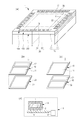
本実施形態の半導体装置の一例としての光電変換装置を、図1を用いて説明する。図1(a)は半導体装置の主要部である半導体デバイス1の斜視図である。図1(b)、(c)は半導体デバイス1の一例の分解斜視図である。図1(d)は半導体デバイス1を含む半導体装置3および電子機器5の模式図である。   A photoelectric conversion device as an example of the semiconductor device of this embodiment will be described with reference to FIG. FIG. 1A is a perspective view of a semiconductor device 1 which is a main part of the semiconductor device. FIGS. 1B and 1C are exploded perspective views of an example of the semiconductor device 1. FIG. 1D is a schematic diagram of the semiconductor device 3 including the semiconductor device 1 and the electronic apparatus 5.

図1(a)に示した半導体デバイス1においては、図1(b)または図1(c)に示したように、第1部分10と第2部分20が重なっている。本実施形態は、主に、第1部分10と第2部分20との電気的接続を得るための導電部材に関する。第1部分10は、第1素子部30と第1配線部31によりなる。第2部分20は第2素子部50と第2配線部51よりなる。第2配線部51が第1部分10と第2素子部50との間に位置する。本実施形態では、第1部分10の第1配線部31が第1素子部30と第2素子部との間に位置するが、第1部分10の第1素子部30が第1配線部31と第2素子部50との間に位置してもよい。   In the semiconductor device 1 shown in FIG. 1A, as shown in FIG. 1B or FIG. 1C, the first portion 10 and the second portion 20 overlap. The present embodiment mainly relates to a conductive member for obtaining an electrical connection between the first portion 10 and the second portion 20. The first portion 10 includes a first element unit 30 and a first wiring unit 31. The second portion 20 includes a second element unit 50 and a second wiring unit 51. The second wiring part 51 is located between the first part 10 and the second element part 50. In the present embodiment, the first wiring portion 31 of the first portion 10 is located between the first element portion 30 and the second element portion, but the first element portion 30 of the first portion 10 is the first wiring portion 31. And the second element unit 50 may be located.

本実施形態では、第1部分10は入射光に応じて信号電荷が発生する光電変換ユニット11を有する。光電変換ユニット11は光電変換素子を含む。光電変換ユニット11は光電変換素子で発生した信号電荷に基づく電気信号を生成する信号生成回路を含み得る。信号生成回路は、例えば、増幅トランジスタや転送トランジスタ、リセットトランジスタ、選択トランジスタを含む。他の例の光電変換ユニット11は、光電変換素子と信号電荷を転送するためのCCD(Charge Coupled Device:電荷結合素子)を含み得る。   In this embodiment, the 1st part 10 has the photoelectric conversion unit 11 which a signal charge generate | occur | produces according to incident light. The photoelectric conversion unit 11 includes a photoelectric conversion element. The photoelectric conversion unit 11 may include a signal generation circuit that generates an electric signal based on signal charges generated by the photoelectric conversion element. The signal generation circuit includes, for example, an amplification transistor, a transfer transistor, a reset transistor, and a selection transistor. The photoelectric conversion unit 11 of another example may include a CCD (Charge Coupled Device) for transferring signal charges with the photoelectric conversion element.

本実施形態では、第2部分20は、信号処理ユニット22を有する。信号処理ユニット22は、光電変換ユニット11で発生した信号電荷に基づく電気信号を処理する。信号処理ユニット22は、ノイズ除去回路、増幅回路、変換回路、画像処理回路を含むことができる。ノイズ除去回路は、例えばCDS(Correlated Double Sampling:相関二重サンプリング)回路である。増幅回路は、例えば列アンプ回路である。変換回路は、例えばコンパレータとカウンタで構成されたADC(Analog Digital Converter:アナログデジタル変換)回路である。画像信号処理回路は、例えばメモリとプロセッサを含み、アナログデジタル変換されたデジタル信号から画像データを生成したり、画像データに画像処理を施したりする。   In the present embodiment, the second portion 20 includes a signal processing unit 22. The signal processing unit 22 processes an electrical signal based on the signal charge generated by the photoelectric conversion unit 11. The signal processing unit 22 can include a noise removal circuit, an amplification circuit, a conversion circuit, and an image processing circuit. The noise removal circuit is, for example, a CDS (Correlated Double Sampling) circuit. The amplifier circuit is, for example, a column amplifier circuit. The conversion circuit is, for example, an ADC (Analog Digital Converter) circuit including a comparator and a counter. The image signal processing circuit includes, for example, a memory and a processor, and generates image data from a digital signal subjected to analog-digital conversion, and performs image processing on the image data.

図1(a)では、光電変換ユニット11の位置を一点鎖線で囲んで示し、信号処理ユニット22の位置を二点鎖線で囲んで示している。ここでは光電変換ユニット11の、第2部分20への正射影領域の一部に信号処理ユニット22の一部が位置している。しかし、光電変換ユニット11の第2部分20への正射影領域の全部に信号処理ユニット22の全部または一部が位置していてもよい。あるいは、第2部分20における光電変換ユニット11の正射影領域の一部に、信号処理ユニット22の全部または一部が位置していてもよい。なお、信号処理ユニット22の一部が第1部分10に設けられていてもよい。例えば、ノイズ除去回路や増幅回路などアナログ信号用の信号処理ユニットを第1部分10に設け、変換回路や画像処理回路などデジタル信号用の信号処理ユニットを第2部分20に設けることもできる。   In FIG. 1A, the position of the photoelectric conversion unit 11 is surrounded by a one-dot chain line, and the position of the signal processing unit 22 is surrounded by a two-dot chain line. Here, a part of the signal processing unit 22 is located in a part of the orthogonal projection area to the second part 20 of the photoelectric conversion unit 11. However, all or part of the signal processing unit 22 may be located in the entire orthogonal projection region onto the second portion 20 of the photoelectric conversion unit 11. Alternatively, all or part of the signal processing unit 22 may be located in a part of the orthogonal projection region of the photoelectric conversion unit 11 in the second portion 20. A part of the signal processing unit 22 may be provided in the first portion 10. For example, a signal processing unit for analog signals such as a noise removal circuit and an amplifier circuit may be provided in the first portion 10, and a signal processing unit for digital signals such as a conversion circuit and an image processing circuit may be provided in the second portion 20.

図1(b)、(c)に示す様に、半導体デバイス1は、光電変換ユニット11を制御する制御ユニット12、および/または、信号処理ユニット22を制御する制御ユニット21を更に備えることができる。これら制御ユニットは、第1部分10と第2部分20の少なくとも一方に設けることができる。図1(b)に示した例では制御ユニット12が第1部分10に設けられており、図1(c)に示した例では制御ユニット21が第2部分20に設けられている。光電変換ユニット11用の制御ユニットを第1部分10に、信号処理ユニット22用の制御ユニットを第2部分20に分けて設けることもできる。制御ユニット12は垂直走査線を介して画素回路に駆動信号を供給する垂直駆動回路や、電源回路を含み得る。制御ユニット21は信号処理ユニット22を駆動するためのタイミング発生回路や、変換回路へ参照信号を供給する参照信号供給回路、増幅回路あるいは変換回路から信号を順次読み出すための水平走査回路を含み得る。   As shown in FIGS. 1B and 1C, the semiconductor device 1 can further include a control unit 12 that controls the photoelectric conversion unit 11 and / or a control unit 21 that controls the signal processing unit 22. . These control units can be provided in at least one of the first portion 10 and the second portion 20. In the example shown in FIG. 1B, the control unit 12 is provided in the first portion 10, and in the example shown in FIG. 1C, the control unit 21 is provided in the second portion 20. The control unit for the photoelectric conversion unit 11 can be provided in the first part 10 and the control unit for the signal processing unit 22 can be provided in the second part 20 separately. The control unit 12 may include a vertical driving circuit that supplies a driving signal to the pixel circuit via a vertical scanning line, and a power supply circuit. The control unit 21 may include a timing generation circuit for driving the signal processing unit 22, a reference signal supply circuit for supplying a reference signal to the conversion circuit, an amplifying circuit, or a horizontal scanning circuit for sequentially reading signals from the conversion circuit.

図1(d)に示す様に、半導体装置3は、半導体デバイス1の1次実装用の実装部材として、パッケージ2を含むことができる。半導体デバイス1はこのパッケージにダイボンドされ、収容されうる。パッケージ2はPGA(Pin Grid Arryay)やLGA(Land Grid Arryay)、BGA(Ball Grid Arryay)、リードフレーム等の外部端子を含み得る。図1(d)に示す様に、半導体装置3は、2次実装用の実装部材として、回路基板4を含むことができる。パッケージ2はこの回路基板4に実装されうる。回路基板4は、リジッド基板、フレキシブル基板あるいはリジッドフレキシブル基板等のプリント基板でありうる。光電変換装置としての半導体装置3は半導体デバイス1に光を導くための光学系を含みうる。   As shown in FIG. 1D, the semiconductor device 3 can include a package 2 as a mounting member for primary mounting of the semiconductor device 1. The semiconductor device 1 can be die-bonded and accommodated in this package. The package 2 may include external terminals such as PGA (Pin Grid Array), LGA (Land Grid Array), BGA (Ball Grid Array), and lead frame. As shown in FIG. 1D, the semiconductor device 3 can include a circuit board 4 as a mounting member for secondary mounting. The package 2 can be mounted on the circuit board 4. The circuit board 4 may be a printed board such as a rigid board, a flexible board, or a rigid flexible board. The semiconductor device 3 as a photoelectric conversion device can include an optical system for guiding light to the semiconductor device 1.

半導体装置3は、種々の電子機器に搭載が可能である。電子機器5は半導体装置3に加えて、演算装置、記憶装置、記録装置、通信装置あるいは表示装置などの周辺装置6を備える。これら周辺装置は、半導体装置3と接続されて、直接的にあるいは間接的に信号のやり取りをおこなう。電子機器5としては、携帯電話やパーソナルコンピュータなどの情報端末、カメラやディスプレイなどの映像機器などが挙げられる。勿論、カメラ付きの情報端末なども含まれる。   The semiconductor device 3 can be mounted on various electronic devices. In addition to the semiconductor device 3, the electronic device 5 includes a peripheral device 6 such as an arithmetic device, a storage device, a recording device, a communication device, or a display device. These peripheral devices are connected to the semiconductor device 3 and exchange signals directly or indirectly. Examples of the electronic device 5 include information terminals such as mobile phones and personal computers, and video devices such as cameras and displays. Of course, an information terminal with a camera is also included.

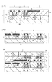
半導体デバイス1の一例の詳細を、図2を用いて説明する。図2は、図1(a)に示した点Pと点Qを含む面における半導体デバイス1の断面図である。なお、図2は図1(b)の様に、制御ユニット12を有する例である。   Details of an example of the semiconductor device 1 will be described with reference to FIG. FIG. 2 is a cross-sectional view of the semiconductor device 1 in a plane including the points P and Q shown in FIG. 2 is an example having a control unit 12 as shown in FIG.

以下の説明において、導電体層は半導体層よりも導電率の高い材料からなるものとし、絶縁体層は半導体層よりも導電率の低い材料からなるものとする。   In the following description, it is assumed that the conductor layer is made of a material having higher conductivity than the semiconductor layer, and the insulator layer is made of a material having lower conductivity than the semiconductor layer.

また、以下の半導体化合物や金属化合物の説明において、炭化窒化物および酸化窒化物は窒化物に含める。窒化炭化物および酸化炭化物は炭化物に含める。   In the following description of semiconductor compounds and metal compounds, carbonitrides and oxynitrides are included in nitrides. Nitride carbide and oxycarbide are included in the carbide.

まず、第1部分10について、第1素子部30と第1配線部31のそれぞれの構成を説明する。   First, regarding the first portion 10, the configurations of the first element unit 30 and the first wiring unit 31 will be described.

第1素子部30は第1半導体層303を含む。第1半導体層303は例えばシリコン層である。第1素子部30は、図1(b)における光電変換ユニット11を構成する半導体素子(光電変換素子)として第1半導体層303に設けられたフォトダイオードPDを有する。フォトダイオードPDは、第1半導体層303のp型半導体領域32とn型半導体領域34とp型半導体領域35を含む。光電変換素子はフォトゲートでもよい。光電変換ユニット11は光電変換素子で発生した信号電荷に基づく電気信号を生成する信号生成回路を含み得る。信号生成回路は、MOSトランジスタ等の半導体素子で構成することができる。図2には、第1部分10の光電変換ユニット11の転送トランジスタTr1と、リセットトランジスタTr2とを示している。また、図1(b)における第1部分10の制御ユニット12の半導体素子として、トランジスタTr3、Tr4とを示している。   The first element unit 30 includes a first semiconductor layer 303. The first semiconductor layer 303 is, for example, a silicon layer. The first element unit 30 includes a photodiode PD provided in the first semiconductor layer 303 as a semiconductor element (photoelectric conversion element) constituting the photoelectric conversion unit 11 in FIG. The photodiode PD includes a p-type semiconductor region 32, an n-type semiconductor region 34, and a p-type semiconductor region 35 of the first semiconductor layer 303. The photoelectric conversion element may be a photogate. The photoelectric conversion unit 11 may include a signal generation circuit that generates an electric signal based on signal charges generated by the photoelectric conversion element. The signal generation circuit can be composed of a semiconductor element such as a MOS transistor. FIG. 2 shows the transfer transistor Tr1 and the reset transistor Tr2 of the photoelectric conversion unit 11 of the first portion 10. Further, transistors Tr3 and Tr4 are shown as semiconductor elements of the control unit 12 of the first portion 10 in FIG.

本例では、第1素子部30を構成する第1半導体層303の表面103の一部はMOSトランジスタTr1、Tr2、Tr3、Tr4のゲート絶縁膜と界面を成している。第1素子部30にはSTI(Shallow Trench Isolation)やLOCOS(LOCal Oxidation of Silicon)などの素子分離38が設けられている。第1半導体層303の上には、第1半導体層303の表面103を保護する、窒化シリコンや酸化シリコンなどの絶縁体層からなる第1保護膜(不図示)が設けられている。このように、第1素子部30は第1半導体層303に加えて、素子分離38やゲート絶縁膜、ゲート電極、第1保護膜を含み得る。   In this example, a part of the surface 103 of the first semiconductor layer 303 constituting the first element unit 30 forms an interface with the gate insulating films of the MOS transistors Tr1, Tr2, Tr3, Tr4. The first element unit 30 is provided with an element isolation 38 such as STI (Shallow Trench Isolation) or LOCOS (LOCal Oxidation of Silicon). A first protective film (not shown) made of an insulating layer such as silicon nitride or silicon oxide is provided on the first semiconductor layer 303 to protect the surface 103 of the first semiconductor layer 303. As described above, the first element unit 30 may include the element isolation 38, the gate insulating film, the gate electrode, and the first protective film in addition to the first semiconductor layer 303.

第1配線部31は、導電体層および絶縁体層を含む。第1配線部31は複数の配線レベルを有しうる。1つの配線レベルは、配線パターンとプラグを有しうる。典型的な導電体層は配線パターンを構成する。さらに典型的な導電体層は配線パターンの内で電流密度の大きい主導電層を構成するが、導電体層は配線パターンの内で主導電層よりも電流密度の小さい副導電層を構成する場合もある。導電体層は下の配線レベルとの導通を得るためのビアプラグ、あるいは第1素子部30との導通を得るためのコンタクトプラグを構成する場合もある。   The first wiring part 31 includes a conductor layer and an insulator layer. The first wiring unit 31 can have a plurality of wiring levels. One wiring level can have a wiring pattern and a plug. A typical conductor layer constitutes a wiring pattern. Furthermore, a typical conductor layer constitutes a main conductive layer having a high current density in the wiring pattern, but the conductor layer constitutes a sub conductive layer having a current density smaller than that of the main conductive layer in the wiring pattern. There is also. The conductor layer may constitute a via plug for obtaining conduction with the lower wiring level or a contact plug for obtaining conduction with the first element unit 30.

ビアプラグやコンタクトプラグもまた、主導電層と副導電層で構成され得る。これら副導電層は典型的にはバリアメタルでありうる。バリアメタルのバリア機能としては、主導電層と絶縁体層との間での拡散に対するバリア、或いは主導電層と絶縁体層との間の反応に対するバリアが挙げられる。しかし、「バリアメタル」は、副導電層に与えられる便宜的な呼称であって何らかのバリア機能を有しているとは限らない。バリアメタルは、これらのバリア機能を必要としない場合であっても、単に主導電層を形成する際の下地としてや、エレクトロマイグレーションやストレスマイグレーションの緩和などを目的として用いられうる。   Via plugs and contact plugs can also be composed of a main conductive layer and a sub conductive layer. These sub-conductive layers can typically be barrier metals. The barrier function of the barrier metal includes a barrier against diffusion between the main conductive layer and the insulator layer, or a barrier against reaction between the main conductive layer and the insulator layer. However, “barrier metal” is a convenient name given to the sub-conductive layer and does not necessarily have any barrier function. Even when these barrier functions are not required, the barrier metal can be used simply as a base for forming the main conductive layer or for the purpose of mitigating electromigration or stress migration.

絶縁体層は同じ配線レベルの配線パターン同士を絶縁する配線間絶縁層および/または異なる配線レベルの配線パターン同士を絶縁する層間絶縁層として機能し得る。第1配線部31は1層以上の導電体層で構成された、多数の電気経路(配線)を有する。一つの配線は、コンタクトプラグ、ビアプラグおよび配線パターンで構成されうる。   The insulator layer can function as an inter-wiring insulating layer that insulates wiring patterns at the same wiring level and / or an interlayer insulating layer that insulates wiring patterns at different wiring levels. The first wiring part 31 has a large number of electrical paths (wirings) composed of one or more conductor layers. One wiring can be composed of a contact plug, a via plug, and a wiring pattern.

第1配線部31の詳細な構成を説明する。第1配線部31には、コンタクトプラグ44と、配線パターン40a、40b、40cおよびビアプラグが設けられている。導電体層で構成されたこれらコンタクトプラグ、配線パターン、ビアプラグが多数の電気経路を構成する。コンタクトプラグ44は主にタングステン層からなり、タングステン層に加えて、チタン層および/または窒化チタン層を含むバリアメタルを有する。配線パターン40a、40b、40cおよびビアプラグは主に銅層からなり、銅層に加えて、窒化タンタル層および/またはタンタル層を含むバリアメタルを有する。配線パターン40aは1つの銅層で構成され、配線パターン40bとビアプラグ、および配線パターン40cとビアプラグは、それぞれ1つの銅層で一体的に構成される。本例の第1配線311は、配線パターン40cを含んでおり、半導体素子とは、不図示の部分で、コンタクトプラグ44と、配線パターン40a、40bおよびビアプラグを介して接続されている。   A detailed configuration of the first wiring unit 31 will be described. The first wiring part 31 is provided with contact plugs 44, wiring patterns 40a, 40b, 40c and via plugs. These contact plugs, wiring patterns, and via plugs formed of a conductor layer constitute a large number of electrical paths. The contact plug 44 is mainly made of a tungsten layer, and has a barrier metal including a titanium layer and / or a titanium nitride layer in addition to the tungsten layer. The wiring patterns 40a, 40b, 40c and the via plug are mainly made of a copper layer, and have a barrier metal including a tantalum nitride layer and / or a tantalum layer in addition to the copper layer. The wiring pattern 40a is composed of one copper layer, and the wiring pattern 40b and the via plug, and the wiring pattern 40c and via plug are each integrally composed of one copper layer. The first wiring 311 of this example includes a wiring pattern 40c, and is connected to a semiconductor element through a contact plug 44, wiring patterns 40a and 40b, and a via plug at a portion not shown.

第1配線部31には、層間絶縁層あるいは配線間絶縁層としての、主に酸化シリコンからなる絶縁体層を含む絶縁体膜39が設けられている。典型的な絶縁体膜39は複数の絶縁体層を有する多層膜である。第1配線部31の絶縁体膜39は、窒化シリコン、炭化シリコンなどからなる不図示の絶縁体層を、配線パターン40a、40b、40cに含有される銅の拡散防止層としてさらに有することができる。これらは、層間絶縁層と配線パターンの間に配され得る。   The first wiring portion 31 is provided with an insulator film 39 including an insulator layer mainly made of silicon oxide as an interlayer insulating layer or an inter-wiring insulating layer. A typical insulator film 39 is a multilayer film having a plurality of insulator layers. The insulator film 39 of the first wiring part 31 can further have an insulator layer (not shown) made of silicon nitride, silicon carbide or the like as a copper diffusion prevention layer contained in the wiring patterns 40a, 40b, and 40c. . These can be arranged between the interlayer insulating layer and the wiring pattern.

次に、第2部分20について、第2素子部50と第2配線部51のそれぞれの構成を説明する。   Next, regarding the second portion 20, the configurations of the second element unit 50 and the second wiring unit 51 will be described.

第2素子部50は第2半導体層505を含み、信号処理ユニット22を構成する半導体素子としてのMOSトランジスタTr5、Tr6、Tr7、Tr8を有する。本例では、第2半導体層505の表面203の一部は、MOSトランジスタTr5、Tr6、Tr7、Tr8のゲート絶縁膜と界面を成している。第2素子部50にはSTIやLOCOSなどの素子分離58が設けられている。第2半導体層505の上には、第2半導体層505の表面203を保護する窒化シリコンや酸化シリコンなどの絶縁体からなる第2保護膜(不図示)が設けられている。第2素子部50は第2半導体層505に加えて、素子分離58やゲート絶縁膜、ゲート電極、第2保護膜を含み得る。   The second element unit 50 includes a second semiconductor layer 505 and includes MOS transistors Tr5, Tr6, Tr7, Tr8 as semiconductor elements constituting the signal processing unit 22. In this example, a part of the surface 203 of the second semiconductor layer 505 forms an interface with the gate insulating films of the MOS transistors Tr5, Tr6, Tr7, Tr8. The second element unit 50 is provided with an element isolation 58 such as STI or LOCOS. A second protective film (not shown) made of an insulator such as silicon nitride or silicon oxide that protects the surface 203 of the second semiconductor layer 505 is provided on the second semiconductor layer 505. In addition to the second semiconductor layer 505, the second element unit 50 may include an element isolation 58, a gate insulating film, a gate electrode, and a second protective film.

第2配線部51は、導電体層および絶縁体層を含む。第2配線部51の導電体層および絶縁体層も、第1配線部31の導電体層および絶縁体層と同様の機能を有する。   The second wiring part 51 includes a conductor layer and an insulator layer. The conductor layer and the insulator layer of the second wiring part 51 also have the same functions as the conductor layer and the insulator layer of the first wiring part 31.

第2配線部51の詳細な構成を説明する。第2配線部51には、コンタクトプラグ54aと、複数の配線パターン53a、53b、53cおよびビアプラグ54b、54cが設けられている。導電体層で構成されたこれらコンタクトプラグ、配線パターン、ビアプラグが多数の電気経路を構成する。コンタクトプラグ54aとビアプラグ54cは主にタングステン層からなり、タングステン層に加えて、チタン層および/または窒化チタン層を含むバリアメタルを有する。配線パターン53a、53bおよびビアプラグ54bは主に銅層からなり、銅層に加えて、窒化タンタル層および/またはタンタル層を含むバリアメタルを有する。配線パターン53aは1つの銅層を含み構成される。配線パターン53bとビアプラグ54bは、1つの銅層で一体的に構成される。配線パターン53cは主にアルミニウム層からなり、アルニミウム層に加えて、チタン層および/または窒化チタン層を含むバリアメタルを有する。本例の第2配線512は、配線パターン53cを含んでおり、半導体素子とは、不図示のコンタクトプラグ54aと、配線パターン53a、53bおよびビアプラグ54b、54cを介して接続されている。   A detailed configuration of the second wiring unit 51 will be described. The second wiring portion 51 is provided with a contact plug 54a, a plurality of wiring patterns 53a, 53b, 53c and via plugs 54b, 54c. These contact plugs, wiring patterns, and via plugs formed of a conductor layer constitute a large number of electrical paths. The contact plug 54a and the via plug 54c are mainly made of a tungsten layer, and have a barrier metal including a titanium layer and / or a titanium nitride layer in addition to the tungsten layer. The wiring patterns 53a and 53b and the via plug 54b are mainly made of a copper layer, and have a barrier metal including a tantalum nitride layer and / or a tantalum layer in addition to the copper layer. The wiring pattern 53a includes one copper layer. The wiring pattern 53b and the via plug 54b are integrally formed of one copper layer. The wiring pattern 53c is mainly made of an aluminum layer, and has a barrier metal including a titanium layer and / or a titanium nitride layer in addition to the aluminum layer. The second wiring 512 of this example includes a wiring pattern 53c, and is connected to a semiconductor element via a contact plug 54a (not shown), wiring patterns 53a and 53b, and via plugs 54b and 54c.

第2配線部51には、層間絶縁層あるいは配線間絶縁層として、主に酸化シリコンからなる絶縁体層を含む絶縁体膜49が設けられている。典型的な絶縁体膜49は複数の絶縁体層を有する多層膜である。第2配線部51の絶縁体膜49は窒化シリコンや炭化シリコンからなる不図示の絶縁体層を、配線パターン53a、53bに含有される銅の拡散防止層としてさらに有することができる。これらは、層間絶縁層と配線パターンの間に配され得る。   The second wiring portion 51 is provided with an insulator film 49 including an insulator layer mainly made of silicon oxide as an interlayer insulating layer or an inter-wiring insulating layer. A typical insulator film 49 is a multilayer film having a plurality of insulator layers. The insulating film 49 of the second wiring portion 51 can further include an insulating layer (not shown) made of silicon nitride or silicon carbide as a copper diffusion preventing layer contained in the wiring patterns 53a and 53b. These can be arranged between the interlayer insulating layer and the wiring pattern.

第1配線部31と第2配線部51の配線パターン40a、40b、40c、53a、53bやプラグにおいて、銅層やタングステン層、アルミニウム層は、配線における導電率の高い主導電層として機能する。主導電層は、バリアメタルに用いられるタンタル層や窒化タンタル層、チタン層、窒化チタン層などの副導電層よりも導電率の高い材料からなり、また、電流が流れる方向における断面積が小さく、低抵抗である。   In the wiring patterns 40a, 40b, 40c, 53a, 53b and the plugs of the first wiring part 31 and the second wiring part 51, the copper layer, the tungsten layer, and the aluminum layer function as a main conductive layer having high conductivity in the wiring. The main conductive layer is made of a material having higher conductivity than the sub-conductive layer such as a tantalum layer, a tantalum nitride layer, a titanium layer, or a titanium nitride layer used for the barrier metal, and has a small cross-sectional area in the direction in which the current flows. Low resistance.

配線パターン40a、40b、40c、53a、53bが主に銅層からなる例を示したが、これらには、配線パターン53cの様に、主にアルミニウム層からなる配線パターンを採用することもできる。なお、銅層やアルミニウム層は単体の銅のみならず、他の金属が添加された合金であってもよい。例えば、銅層は銅よりも少ないアルミニウムやシリコンなどを添加物として含み得るし、アルミニウム層はアルミニウムより少ない銅やシリコンなどを添加物として含み得る。絶縁体膜39の主たる絶縁体層が酸化シリコンからなる例を挙げたが、BSGやPSG、BPSGなどのケイ酸塩ガラスを用いることもできる。また、酸化シリコンよりも低誘電率の低い材料(low−k材料)を用いることもできる。   Although the wiring pattern 40a, 40b, 40c, 53a, 53b has shown the example which mainly consists of a copper layer, the wiring pattern which mainly consists of an aluminum layer like the wiring pattern 53c can also be employ | adopted for these. The copper layer and the aluminum layer may be not only single copper but also an alloy to which other metals are added. For example, the copper layer may contain less aluminum, silicon, or the like than copper, and the aluminum layer may contain less copper, silicon, or the like than aluminum. Although the example in which the main insulator layer of the insulator film 39 is made of silicon oxide has been given, silicate glass such as BSG, PSG, or BPSG can also be used. Alternatively, a material having a lower dielectric constant than silicon oxide (low-k material) can be used.

第1配線部31の配線パターンを配線パターン40a、40b、40cの3レベル、第2配線部51の配線パターンは53a、53b、53cの3レベルとする例を示した。しかし、配線パターンのレベル数は適宜設定可能であり、第1配線部31と第2配線部51とで異なっていてもよい。例えば、第2配線部51の配線パターンのレベル数を第1配線部31の配線パターンのレベル数よりも多くしてもよい。   The example in which the wiring pattern of the first wiring part 31 is three levels of wiring patterns 40a, 40b, and 40c and the wiring pattern of the second wiring part 51 is three levels of 53a, 53b, and 53c is shown. However, the number of levels of the wiring pattern can be set as appropriate, and may be different between the first wiring part 31 and the second wiring part 51. For example, the number of levels of the wiring pattern of the second wiring unit 51 may be larger than the number of levels of the wiring pattern of the first wiring unit 31.

続いて、電子デバイス1の他の構造について説明する。   Subsequently, another structure of the electronic device 1 will be described.

第1部分10と第2部分20は、第1配線部31と第2配線部51とで接合されている。第1配線部31の絶縁体膜39と第2配線部51の絶縁体膜49が、接合面60を介して接合されている。   The first portion 10 and the second portion 20 are joined by the first wiring portion 31 and the second wiring portion 51. The insulator film 39 of the first wiring part 31 and the insulator film 49 of the second wiring part 51 are joined via the joint surface 60.

本例の半導体デバイス1は、第1半導体層303のトランジスタTr1〜4が設けられた面(表面103)とは反対側の面(裏面104)が受光面となる裏面照射型の光電変換装置を構成する。裏面照射型の光電変換装置において、第1部分10の第1半導体層303の厚みは10μm未満であり、例えば2〜5μmである。第2半導体層505の厚みは第1半導体層303よりも厚く、第2半導体層505は第1半導体層303の支持体として機能する。第2半導体層505の厚みは10μm以上であり、例えば20〜500μmである。   The semiconductor device 1 of this example is a back-illuminated photoelectric conversion device in which a surface (back surface 104) opposite to the surface (front surface 103) on which the transistors Tr1 to Tr4 of the first semiconductor layer 303 are provided is a light receiving surface. Configure. In the back-illuminated photoelectric conversion device, the thickness of the first semiconductor layer 303 of the first portion 10 is less than 10 μm, for example, 2 to 5 μm. The thickness of the second semiconductor layer 505 is thicker than that of the first semiconductor layer 303, and the second semiconductor layer 505 functions as a support for the first semiconductor layer 303. The thickness of the second semiconductor layer 505 is 10 μm or more, for example, 20 to 500 μm.

第1半導体層303の裏面104側には、光学部材41が設けられている。   An optical member 41 is provided on the back surface 104 side of the first semiconductor layer 303.

光学部材41は、反射防止層61、絶縁体層62、遮光層63、絶縁体層69、平坦化層71、カラーフィルタアレイ73およびマイクロレンズアレイ74を含みうる。光学部材41は第1素子部30の受光面(裏面104)を構成するp型半導体領域32に接触している。光学部材41は第1素子部30側とは反対側に光入射面401を有する。本例では光入射面401はマイクロレンズアレイ74で構成されている。   The optical member 41 can include an antireflection layer 61, an insulator layer 62, a light shielding layer 63, an insulator layer 69, a planarizing layer 71, a color filter array 73, and a microlens array 74. The optical member 41 is in contact with the p-type semiconductor region 32 constituting the light receiving surface (back surface 104) of the first element unit 30. The optical member 41 has a light incident surface 401 on the side opposite to the first element unit 30 side. In this example, the light incident surface 401 is constituted by a microlens array 74.

電極パッド78は配線パターン53cと同レベルの層に配されている。電極パッド78の上には、複数の絶縁体層、第1半導体層303、光学部材41を貫通する開口77が設けられている。開口77には、電極パッド78に接続するボンディングワイヤ79が設けられている。ワイヤボンディングはパッケージの内部端子に接続される。なお、半導体デバイス1とパッケージの接続には、ワイヤボンディング接続に限らず、フリップチップ接続を用いることもできる。   The electrode pads 78 are arranged on the same level as the wiring pattern 53c. On the electrode pad 78, an opening 77 that penetrates the plurality of insulator layers, the first semiconductor layer 303, and the optical member 41 is provided. A bonding wire 79 connected to the electrode pad 78 is provided in the opening 77. Wire bonding is connected to the internal terminals of the package. Note that the connection between the semiconductor device 1 and the package is not limited to wire bonding, and flip-chip connection can also be used.

半導体デバイス1には、第1配線311と第2配線512を相互に接続する導電部材68が設けられている。導電部材68を構成する導電材料は、金、銀、銅、アルミニウム、タングステン、タンタル、チタン、マンガン、或いはこれらの窒化物や炭化物などの化合物である。   The semiconductor device 1 is provided with a conductive member 68 that connects the first wiring 311 and the second wiring 512 to each other. The conductive material constituting the conductive member 68 is gold, silver, copper, aluminum, tungsten, tantalum, titanium, manganese, or a compound such as nitride or carbide thereof.

導電部材68は、第1素子部30の第1半導体層303を貫通して第1配線部31の第1配線311に接続し、さらに、第1配線部31を貫通して第2配線部51の第2配線512に接続する。本例では、導電部材68は第1配線311の配線パターン40cに接触し、第2配線512の配線パターン53cに接触する。本実施形態では、導電部材68は第1配線311の配線パターン40cの複数の部分の間に位置しうる。換言すれば、配線パターン40cの複数の部分が導電部材68を挟む。配線パターン40cの導電部材68を挟む複数の部分は、導電部材68に対向する部分(対向部分)である。導電部材68の配線パターン40cの複数の部分の間に位置する部分は、第1配線部31を貫通する部分である。導電部材68を挟む、配線パターン40cの複数の部分(対向部分)は、第2配線512の配線パターン53cに重なっていることが好ましいが、重なっていなくてもよい。2つの配線パターン40c、53cの重なり合う部分は、一方の配線パターンの、他方の配線パターンに重なる部分である。ここで、配線パターンが重なり合うことは、第1半導体層303から第2半導体層505に向かう方向(第1半導体層303と第2半導体層505の法線方向)において、複数の配線パターンが位置することを意味する。   The conductive member 68 passes through the first semiconductor layer 303 of the first element unit 30 and is connected to the first wiring 311 of the first wiring unit 31, and further penetrates the first wiring unit 31 to form the second wiring unit 51. The second wiring 512 is connected. In this example, the conductive member 68 contacts the wiring pattern 40 c of the first wiring 311 and contacts the wiring pattern 53 c of the second wiring 512. In the present embodiment, the conductive member 68 can be positioned between a plurality of portions of the wiring pattern 40 c of the first wiring 311. In other words, the plurality of portions of the wiring pattern 40 c sandwich the conductive member 68. A plurality of portions sandwiching the conductive member 68 of the wiring pattern 40 c are portions (opposed portions) facing the conductive member 68. A portion located between the plurality of portions of the wiring pattern 40 c of the conductive member 68 is a portion that penetrates the first wiring portion 31. A plurality of portions (opposing portions) of the wiring pattern 40c sandwiching the conductive member 68 preferably overlap with the wiring pattern 53c of the second wiring 512, but may not overlap. The overlapping part of the two wiring patterns 40c and 53c is a part of one wiring pattern that overlaps the other wiring pattern. Here, the overlapping of the wiring patterns means that a plurality of wiring patterns are located in the direction from the first semiconductor layer 303 toward the second semiconductor layer 505 (the normal direction of the first semiconductor layer 303 and the second semiconductor layer 505). Means that.

図2(b−1)は導電部材68が第1配線311に囲まれている場合の平面図であり、図2(c−1)はその斜視図である。配線パターン40cは、部分3111、3112、3113、3114を有している。導電部材68は、部分3111と部分3113の間に位置し、部分3112と部分3114との間に位置する。また、導電部材68は、部分3111と部分3112の間に位置し、部分3113と部分3114との間に位置する。これらの部分3111、3112、3113、3114は、第2配線512を構成する配線パターン53cに重なっていることが望ましいが、重なっていなくてもよい。また、これらの部分3111、3112、3113、3114は、導電部材68に接触している。本例では、導電部材68は第1配線311の側面に接触している。この側面は、部分3111、3112、3113、3114で構成される。ここでは、導電部材68は第1配線311の側面に接触している例を挙げたが、導電部材68が第1配線311の側面ではなく第1配線311の上面に接触していてもよい。導電部材68が第1配線311の側面および上面に接していてもよい。   FIG. 2B-1 is a plan view when the conductive member 68 is surrounded by the first wiring 311, and FIG. 2C-1 is a perspective view thereof. The wiring pattern 40 c has portions 3111, 3112, 3113, 3114. The conductive member 68 is located between the portion 3111 and the portion 3113, and is located between the portion 3112 and the portion 3114. The conductive member 68 is located between the portions 3111 and 3112 and is located between the portions 3113 and 3114. These portions 3111, 3112, 3113, and 3114 desirably overlap with the wiring pattern 53 c constituting the second wiring 512, but do not need to overlap. Further, these portions 3111, 3112, 3113, 3114 are in contact with the conductive member 68. In this example, the conductive member 68 is in contact with the side surface of the first wiring 311. This side surface is constituted by portions 3111, 3112, 3113, 3114. Here, the conductive member 68 is in contact with the side surface of the first wiring 311, but the conductive member 68 may be in contact with the upper surface of the first wiring 311 instead of the side surface of the first wiring 311. The conductive member 68 may be in contact with the side surface and the upper surface of the first wiring 311.

図2(b−2)は導電部材68が第1配線311に挟まれている場合の平面図であり、図2(c−2)はその斜視図である。配線パターン40cは、部分3115、3116、3117を有している。導電部材68は、部分3115と部分3117の間に位置する。また、導電部材68は第1配線311の部分3115と部分3116との間に位置し、部分3116と部分3117との間に位置している。図2(b−2)の例では、導電部材68は、第1配線311の連続な3つの部分3115、3116、3117の側面に面している。そして、3つの部分のうちの2組の2部分(部分3115と部分3115、部分3116と部分3117)の側面が成す角度が90°である。また、3つの部分のうちの1組の2部分(部分3115と部分3117)の側面が成す角度が0°(平行)である。図2(b−1)の例と同様に、部分3115、3116、3117は第2配線512を構成する配線パターン53cに重なっている。   FIG. 2B-2 is a plan view when the conductive member 68 is sandwiched between the first wirings 311, and FIG. 2C-2 is a perspective view thereof. The wiring pattern 40 c has portions 3115, 3116, and 3117. The conductive member 68 is located between the portion 3115 and the portion 3117. In addition, the conductive member 68 is located between the portion 3115 and the portion 3116 of the first wiring 311, and is located between the portion 3116 and the portion 3117. In the example of FIG. 2B-2, the conductive member 68 faces the side surfaces of the three continuous portions 3115, 3116, and 3117 of the first wiring 311. Then, the angle formed by the side surfaces of two sets of two portions (portion 3115 and portion 3115, portion 3116 and portion 3117) of the three portions is 90 °. In addition, the angle formed by the side surfaces of a pair of two parts (part 3115 and part 3117) of the three parts is 0 ° (parallel). As in the example of FIG. 2B-1, the portions 3115, 3116, and 3117 overlap with the wiring pattern 53 c constituting the second wiring 512.

図2(b−3)は導電部材68が第1配線311に挟まれている場合の平面図であり、図2(c−3)はその斜視図である。配線パターン40cは、部分3118、3119を有している。2つの部分3118、3119は第1配線311の配線パターン40cの不連続な部分である。図2(b−3)の例では、部分3118、3119は第2配線512の配線パターン53cに重なっている。導電部材68は部分3118、3119の側面に挟まれている。図2(b−3)の例では、導電部材68は、そして、2つの部分3118と部分3119の成す角度が0°(平行)である。図2(b−3)、(c−3)において、導電部材68を挟む第1配線311の2つの部分3114、3115の双方は、仮に導電部材68を絶縁部材に置き換えたとしても、第1配線311の一部であり得る。ここでは、2つの部分3118、3119が配線パターン40c内で電気的に連続している例を示している。しかし、配線パターン40b、40aなど、他の配線レベルを介して2つの部分が電気的に連続して一つの電気経路たる第1配線311を構成していてもよい。   FIG. 2B-3 is a plan view when the conductive member 68 is sandwiched between the first wirings 311. FIG. 2C-3 is a perspective view thereof. The wiring pattern 40 c has portions 3118 and 3119. The two portions 3118 and 3119 are discontinuous portions of the wiring pattern 40 c of the first wiring 311. In the example of FIG. 2B-3, the portions 3118 and 3119 overlap the wiring pattern 53c of the second wiring 512. The conductive member 68 is sandwiched between the side surfaces of the portions 3118 and 3119. In the example of FIG. 2B-3, the conductive member 68 has an angle formed by two portions 3118 and 3119 of 0 ° (parallel). 2B and 2C-3, both of the two portions 3114 and 3115 of the first wiring 311 sandwiching the conductive member 68 are the same even if the conductive member 68 is replaced with an insulating member. It may be a part of the wiring 311. Here, an example is shown in which the two portions 3118 and 3119 are electrically continuous in the wiring pattern 40c. However, two portions such as the wiring patterns 40b and 40a may be electrically connected to each other to form the first wiring 311 as one electric path.

導電部材68が第1配線311の配線パターンの複数の部分の間に位置することは、複数の部分の、導電部材68に向かう面(対向面)同士が成す、導電部材68側の角度が180°未満であることを意味する。つまり、対向面が1つの平面のみで構成されていなければよい。ここでは、複数の平面を組み合わせて対向面を構成した例を示したが、滑らかな曲面等、明確な境界の無い側面に導電部材68が面していてもよい。複数の部分の、導電部材68に向かう面(対向面)が成す、導電部材68側の角度は、90°以下であることが好ましい。例えば、導電部材68が円柱形状で、配線パターン40cの側面が平面視して円弧状であれば、この円弧の中心角が90°以上であることが好ましい。円弧の一端における接線と他端における接線の成す角が90°以上になるためである。   When the conductive member 68 is positioned between the plurality of portions of the wiring pattern of the first wiring 311, the angle on the conductive member 68 side formed by the surfaces (opposing surfaces) facing the conductive member 68 of the plurality of portions is 180. Means less than °. That is, it is only necessary that the opposing surface is composed of only one plane. Here, an example in which the opposing surface is configured by combining a plurality of planes is shown, but the conductive member 68 may face a side surface without a clear boundary such as a smooth curved surface. The angle on the conductive member 68 side formed by a surface (opposing surface) of the plurality of portions facing the conductive member 68 is preferably 90 ° or less. For example, if the conductive member 68 has a cylindrical shape and the side surface of the wiring pattern 40c has an arc shape in plan view, the center angle of the arc is preferably 90 ° or more. This is because the angle formed by the tangent at one end of the arc and the tangent at the other end is 90 ° or more.

導電部材68は配線パターン40a、40b、40cの何れか、もしくは複数に接触しても良く、導電部材68は配線パターン53a、53b、53cの何れか1つ、もしくは複数に接触しても良い。また、導電部材68は、配線パターンの主導電層に接触する場合もあるし、配線パターンのバリアメタルなどの副導電層に接触する場合もある。また、配線パターンのバリアメタルの副導電層を貫通して、主導電層に接触する場合もある。本例では、配線パターン40cの主導電層42であるアルミニウム層の側面、副導電層41a、41bである窒化チタン層(およびチタン層)の側面に接触している。そして、導電部材68は主導電層42の側面に囲まれているか挟まれている。また、配線パターン53cの主導電層56であるアルミニウム層の上面、副導電層55a、55bである窒化チタン層(およびチタン層)の側面に接触している。   The conductive member 68 may be in contact with any one or a plurality of wiring patterns 40a, 40b, and 40c, and the conductive member 68 may be in contact with any one or a plurality of wiring patterns 53a, 53b, and 53c. In addition, the conductive member 68 may be in contact with the main conductive layer of the wiring pattern, or may be in contact with a sub conductive layer such as a barrier metal of the wiring pattern. In some cases, the secondary conductive layer of the barrier metal of the wiring pattern penetrates the main conductive layer. In this example, the side surface of the aluminum layer that is the main conductive layer 42 of the wiring pattern 40c and the side surface of the titanium nitride layer (and titanium layer) that are the sub conductive layers 41a and 41b are in contact. The conductive member 68 is surrounded or sandwiched between the side surfaces of the main conductive layer 42. Further, the upper surface of the aluminum layer which is the main conductive layer 56 of the wiring pattern 53c and the side surface of the titanium nitride layer (and titanium layer) which are the sub conductive layers 55a and 55b are in contact.

本実施形態では、第1配線311と第2配線512の電気経路が第1配線部31と第2配線部51の外を経由することなく、第1配線部31および第2配線部51内に形成されている。これにより、第1配線311と第2配線512との間の配線容量および/または配線抵抗の増大を抑制し、半導体装置を高速に動作させることが可能となる。   In the present embodiment, the electrical paths of the first wiring 311 and the second wiring 512 do not pass through the outside of the first wiring part 31 and the second wiring part 51, and the inside of the first wiring part 31 and the second wiring part 51. Is formed. Thereby, an increase in wiring capacitance and / or wiring resistance between the first wiring 311 and the second wiring 512 can be suppressed, and the semiconductor device can be operated at high speed.

また、第1配線311と導電部材68との電気的接続を、導電部材68の両側に位置する複数の部分で確保することが可能である。そのため、第1配線311と導電部材68との接続不良が生じにくい構造が得られる。接続不良の一因は、使用時の熱サイクルに起因するクラックや、導電部材68や配線パターン40cの腐食や拡散などの化学変化でありうる。また、接続不良の一因は、後述する製造時のアライメントずれでありうる。   In addition, electrical connection between the first wiring 311 and the conductive member 68 can be ensured at a plurality of portions located on both sides of the conductive member 68. As a result, a structure in which poor connection between the first wiring 311 and the conductive member 68 does not occur is obtained. One cause of the connection failure may be a chemical change such as a crack caused by a thermal cycle during use or corrosion or diffusion of the conductive member 68 or the wiring pattern 40c. In addition, a cause of connection failure may be misalignment during manufacturing, which will be described later.

導電部材68は第1半導体層303に設けられた絶縁領域45に囲まれている。本例の絶縁領域45は固体の領域であるが、気体あるいは真空の領域であってもよい。導電部材68により、光電変換ユニット11と信号処理ユニット22、光電変換ユニット11と制御ユニット21あるいは制御ユニット12と信号処理ユニット22とが電気的に接続されている。あるいは、第1部分10に設けられた信号処理ユニットの一部と第2部分20に設けられた信号処理ユニットの一部とが電気的に接続されている。   The conductive member 68 is surrounded by an insulating region 45 provided in the first semiconductor layer 303. The insulating region 45 in this example is a solid region, but may be a gas or vacuum region. The photoelectric conversion unit 11 and the signal processing unit 22, the photoelectric conversion unit 11 and the control unit 21, or the control unit 12 and the signal processing unit 22 are electrically connected by the conductive member 68. Alternatively, a part of the signal processing unit provided in the first part 10 and a part of the signal processing unit provided in the second part 20 are electrically connected.

図2に示したブロック90は部分間の接続に関わる導電部材68、第1配線311、第2配線512、絶縁領域42を含む領域を示している。このブロック90は、複数個が並列に配されることが好ましい。ブロック90が複数に並列に配されることにより、光電変換ユニット11の列毎または行毎の信号を信号処理ユニット22に受け渡し、信号処理ユニット22は光電変換ユニット11で発生した信号電荷に基づく電気信号を処理することが可能となる。またブロック90は縦列に配されてもよいし、縦列と並列を併用してもよい。   A block 90 shown in FIG. 2 shows a region including the conductive member 68, the first wiring 311, the second wiring 512, and the insulating region 42 related to the connection between the parts. A plurality of the blocks 90 are preferably arranged in parallel. By arranging a plurality of blocks 90 in parallel, a signal for each column or row of the photoelectric conversion unit 11 is transferred to the signal processing unit 22, and the signal processing unit 22 is based on signal charges generated by the photoelectric conversion unit 11. The signal can be processed. Further, the blocks 90 may be arranged in columns, or the columns and parallel may be used in combination.

以上が、半導体デバイス1の構成の一例である。これらの構成は、適宜変更することができる。   The above is an example of the configuration of the semiconductor device 1. These configurations can be changed as appropriate.

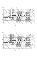
次に、図3、図4を参照しながら本実施形態の半導体装置の製造方法を説明する。図3、図4は、図2と同様の部分(図1の点Pと点Qを含む面)を示す断面図である。   Next, a method for manufacturing the semiconductor device of this embodiment will be described with reference to FIGS. 3 and 4 are cross-sectional views showing the same part (plane including points P and Q in FIG. 1) as in FIG.

図3(a−1)を参照して説明する。第1半導体基板303aを準備する。第1半導体基板303aは例えばシリコン基板である。第1半導体基板303aの第1面(表面)103にSTIなどの素子分離38を形成する。次いで第1半導体基板303aにフォトダイオードPDおよびトランジスタTr1、Tr2、Tr3、Tr4を形成する。このようにして、第1素子部30を形成する。   This will be described with reference to FIG. A first semiconductor substrate 303a is prepared. The first semiconductor substrate 303a is, for example, a silicon substrate. An element isolation 38 such as STI is formed on the first surface (front surface) 103 of the first semiconductor substrate 303a. Next, the photodiode PD and transistors Tr1, Tr2, Tr3, Tr4 are formed on the first semiconductor substrate 303a. In this way, the first element unit 30 is formed.

次いで、第1素子部30の上に層間絶縁層を形成し、層間絶縁層にコンタクトプラグ44を形成する。コンタクトプラグ44に接続するように、シングルダマシン法を用いて配線パターン40aを形成する。さらに層間絶縁層を形成した後、デュアルダマシン法を用いて配線パターン40bおよびビアプラグ、配線パターン40cおよびビアプラグを形成する。その後、配線パターン40cの上に絶縁体膜39の表層となる絶縁体層を形成し、これを平坦化する。このようにして、第1配線部31を形成する。第1配線部31には第1配線311が形成されている。   Next, an interlayer insulating layer is formed on the first element unit 30, and a contact plug 44 is formed in the interlayer insulating layer. A wiring pattern 40 a is formed using a single damascene method so as to be connected to the contact plug 44. Further, after forming an interlayer insulating layer, a wiring pattern 40b and a via plug, a wiring pattern 40c and a via plug are formed by using a dual damascene method. Thereafter, an insulating layer which is a surface layer of the insulating film 39 is formed on the wiring pattern 40c, and is planarized. In this way, the first wiring part 31 is formed. A first wiring 311 is formed in the first wiring portion 31.

以上の様にして、第1部分10となる第1部品10aを作成する。   As described above, the first component 10a to be the first portion 10 is created.

図3(a−2)を参照して説明する。第2半導体基板505aを準備する。第2半導体基板505aは例えばシリコン基板である。第2半導体基板505aの第1面(表面)203にSTIなどの素子分離38を形成する。次いで第2半導体基板505aにTr5、Tr6、Tr7、Tr8を形成する。このようにして、第2素子部50を形成する。   This will be described with reference to FIG. A second semiconductor substrate 505a is prepared. The second semiconductor substrate 505a is, for example, a silicon substrate. An element isolation 38 such as STI is formed on the first surface (front surface) 203 of the second semiconductor substrate 505a. Next, Tr5, Tr6, Tr7, Tr8 are formed on the second semiconductor substrate 505a. In this way, the second element unit 50 is formed.

次いで、第2素子部50の上に層間絶縁層を形成し、層間絶縁層にコンタクトプラグ54aを形成する。コンタクトプラグ54aに接続するように、シングルダマシン法を用いて配線パターン53aを形成する。さらに層間絶縁層を形成した後、デュアルダマシン法を用いて配線パターン53bおよびビアプラグ54b、配線パターン53cおよびビアプラグ54cを形成する。その後、絶縁体膜49の表層となる絶縁体層を形成し、これを平坦化する。このようにして、第2配線部51を形成する。第2配線部51には第2配線512が形成されている。   Next, an interlayer insulating layer is formed on the second element unit 50, and a contact plug 54a is formed in the interlayer insulating layer. A wiring pattern 53a is formed using a single damascene method so as to be connected to the contact plug 54a. Further, after forming the interlayer insulating layer, the wiring pattern 53b and the via plug 54b, the wiring pattern 53c and the via plug 54c are formed by using a dual damascene method. Thereafter, an insulating layer that is a surface layer of the insulating film 49 is formed and planarized. In this way, the second wiring part 51 is formed. A second wiring 512 is formed in the second wiring portion 51.

以上の様にして、第2部分20となる第2部品20aを作成する。   As described above, the second component 20a to be the second portion 20 is created.

図3(b)を参照して説明する。上述のようにして第1部品10aと第2部品20aを用意し、第1部品10aと第2部品20aとを、第1部品10aと第2部品20aとを、第1素子部30と第2素子部50との間に第1配線部31および第2配線部51が位置するように接合する。この接合は、平坦化された絶縁体膜39の表層および絶縁体膜49の表層とのプラズマ接合の他、第1配線部31と第2配線部51の各々の表面に露出した金属層同士の金属接合、或いは接着剤層を介した接着で実現できる。この時、第1配線311の配線パターン40cと第2配線512の配線パターン53cとが重なり合うように接合することが好ましい。第1部品10aと第2部品20aの作製時点で、第1配線311と第2配線512の位置関係を設定しておく。第1配線311の配線パターン40cと第2配線512の配線パターン53cの一方の全部が、他方に重なっていてもよいし、一方の一部が他方に重なっていてもよい。第1配線311の配線パターン40cと第2配線512の配線パターン53cとの間には、平坦化された絶縁体膜39の表層を成す絶縁体層と平坦化された絶縁体膜49の表層を成す絶縁体層とが位置することになる。なお、第1配線部31と第2配線部51の絶縁体膜の少なくとも一方の表層をなす絶縁体層を省略してもよく、配線部の表面に配線パターンが露出していてもよい。   This will be described with reference to FIG. The first component 10a and the second component 20a are prepared as described above, the first component 10a and the second component 20a, the first component 10a and the second component 20a, the first element unit 30 and the second component. It joins so that the 1st wiring part 31 and the 2nd wiring part 51 may be located between the element parts 50. FIG. In addition to the plasma bonding between the planarized surface of the insulator film 39 and the surface layer of the insulator film 49, the bonding is performed between the metal layers exposed on the surfaces of the first wiring portion 31 and the second wiring portion 51. It can be realized by metal bonding or bonding via an adhesive layer. At this time, it is preferable to join the wiring pattern 40c of the first wiring 311 and the wiring pattern 53c of the second wiring 512 so as to overlap each other. At the time of manufacturing the first component 10a and the second component 20a, the positional relationship between the first wiring 311 and the second wiring 512 is set. Either one of the wiring pattern 40c of the first wiring 311 and the wiring pattern 53c of the second wiring 512 may overlap the other, or a part of one may overlap the other. Between the wiring pattern 40c of the first wiring 311 and the wiring pattern 53c of the second wiring 512, an insulating layer that forms a surface layer of the planarized insulating film 39 and a surface layer of the planarized insulating film 49 are provided. The insulator layer to be formed is located. Note that the insulating layer forming at least one surface layer of the insulating film of the first wiring portion 31 and the second wiring portion 51 may be omitted, and the wiring pattern may be exposed on the surface of the wiring portion.

次いで、第1半導体基板303aを、第1素子部30の第1配線部31側とは反対側(裏面側)から、位置104まで薄化することにより、第1半導体層303を得る。この薄化は、CMPなどの研磨やグラインドなどの研削、エッチングなどの周知の方法で行われる。この薄化は、当初の第1半導体基板303aが700μm以上の厚みを有するのに対して、第1半導体基板303aの薄化後における第1半導体層303の厚みが500μm以下、さらには10μm以下となるように行うことが出来る。この時点で、第1半導体層303の厚みは第2半導体層505の厚みよりも小さくされうる。フリップチップ接続を用いる場合などには第2半導体基板505aは薄化することが好ましいが、そのまま第2半導体層505として用いることも可能である。   Next, the first semiconductor layer 303 is obtained by thinning the first semiconductor substrate 303a from the opposite side (back side) of the first element part 30 to the first wiring part 31 side to the position 104. This thinning is performed by a known method such as polishing such as CMP, grinding such as grinding, or etching. In this thinning, the initial first semiconductor substrate 303a has a thickness of 700 μm or more, whereas the thickness of the first semiconductor layer 303 after the thinning of the first semiconductor substrate 303a is 500 μm or less, further 10 μm or less. Can be done. At this point, the thickness of the first semiconductor layer 303 can be made smaller than the thickness of the second semiconductor layer 505. When the flip chip connection is used, the second semiconductor substrate 505a is preferably thinned, but can be used as the second semiconductor layer 505 as it is.

このようにして接合工程が行われ、積層体が得られる。次に、積層体に導電部材を形成することにより、第1配線311と第2配線512とを接続する接続工程が行われる。接続工程は複数の段階を経て行われる。   Thus, a joining process is performed and a laminated body is obtained. Next, a connection step for connecting the first wiring 311 and the second wiring 512 is performed by forming a conductive member in the laminate. The connection process is performed through a plurality of stages.

図4(c)を参照して説明する。第1段階として、絶縁領域45の内側に、第1半導体層303側から接続孔を形成する。この接続孔は、第1半導体層303を貫通し、配線パターン40cに達する直前の深さまで開口する。この接続孔の形成は、絶縁体膜39の絶縁体層の内、配線パターン40cと第1半導体層303との間に位置する絶縁体層のエッチングによって行われる。上述のように第1半導体基板303aを薄化することで、接続孔のアスペクト比を小さくすることが可能となり、微細化が可能である。次に、接続孔の側壁及び底部を含む領域に、例えば酸化シリコンなどの絶縁膜を成膜する。この絶縁膜をエッチバックすることにより、接続孔の側壁のみに絶縁領域59を残す。   This will be described with reference to FIG. As a first step, a connection hole is formed inside the insulating region 45 from the first semiconductor layer 303 side. This connection hole penetrates the first semiconductor layer 303 and opens to a depth just before reaching the wiring pattern 40c. The connection hole is formed by etching an insulator layer located between the wiring pattern 40 c and the first semiconductor layer 303 in the insulator layer of the insulator film 39. By reducing the thickness of the first semiconductor substrate 303a as described above, the aspect ratio of the connection hole can be reduced and miniaturization can be achieved. Next, an insulating film such as silicon oxide is formed in a region including the side wall and the bottom of the connection hole. By etching back the insulating film, the insulating region 59 is left only on the side wall of the connection hole.

さらに接続孔と配線パターン40cの間に位置する残りの絶縁体層をエッチングして接続孔を深くする。接続孔が配線パターン40cに達し、さらに配線パターン40cの一部を、エッチングなどを用いて除去する。詳細には、副導電層41a、主導電層42、副導電層41bの順でエッチングする。配線パターン40cのエッチング条件は、絶縁体層のエッチング条件と異なるものを採用することができる。ここで、配線パターン40cの除去される一部とは、第1配線311を構成する配線パターン40cの、第2配線512の配線パターン53cに重なる部分の一部または全部でありうる。本例では、配線パターン40cの配線パターン53cに重なる部分の一部を除去しており、除去後には、配線パターン53cに重なる部分の残りの一部が残留している。   Further, the remaining insulator layer located between the connection hole and the wiring pattern 40c is etched to deepen the connection hole. The connection hole reaches the wiring pattern 40c, and a part of the wiring pattern 40c is removed by etching or the like. Specifically, the sub conductive layer 41a, the main conductive layer 42, and the sub conductive layer 41b are etched in this order. The etching conditions for the wiring pattern 40c may be different from the etching conditions for the insulator layer. Here, the part of the wiring pattern 40c to be removed may be a part or all of the part of the wiring pattern 40c that constitutes the first wiring 311 that overlaps the wiring pattern 53c of the second wiring 512. In this example, a part of the portion of the wiring pattern 40c that overlaps the wiring pattern 53c is removed, and after the removal, the remaining portion of the portion that overlaps the wiring pattern 53c remains.

さらに絶縁体膜39をエッチングすることにより、接続孔が第1配線部31と第2配線部51の接合面60を通過して、第1部品10aを貫通する。さらに、第2配線部51に形成された配線パターン53cに達するまで絶縁体膜49をエッチングする。この接続孔の形成は、絶縁体膜39の絶縁体層および絶縁体膜49の絶縁体層の内、配線パターン40cと配線パターン53cとの間に位置する絶縁体層のエッチングによって行われる。これらの絶縁体層には絶縁体膜39や絶縁体膜49の表層の絶縁体層が含まれうる。このようにして、第2配線512の配線パターン53cに達する貫通孔67を形成する。これにより、貫通孔67には配線パターン40cの側面が露出し、配線パターン53cの上面が露出する。そして、配線パターン40cの複数の部分の間に貫通孔67が位置する。換言すれば、配線パターン40cの複数の部分は、貫通孔67を介して向かい合う。配線パターン53cの露出される部分とは、接合工程の後の時点で、第2配線512を構成する配線パターン53cの、第1配線311の配線パターン40cに重なっていた部分の一部または全部でありうる。貫通孔67の形成位置を配線パターン40cの輪郭よりも内側に設定することができる。これにより、第1部品10aと第2部品20aとの接合工程あるいは貫通孔67の形成時にアライメントズレが生じていたとしても、配線パターン40cと配線パターン53cの一方に貫通孔67が達しないリスクが軽減される。次いで、薬液によるウェットエッチングにより、露出した配線パターン40c上の堆積物を除去する。ウェットエッチングとしたが、デポ物を除去できる手段であれば、ドライエッチングも可能である。   Further, by etching the insulator film 39, the connection hole passes through the joint surface 60 of the first wiring part 31 and the second wiring part 51 and penetrates the first component 10a. Further, the insulator film 49 is etched until the wiring pattern 53c formed in the second wiring portion 51 is reached. The connection hole is formed by etching the insulating layer located between the wiring pattern 40c and the wiring pattern 53c, among the insulating layer of the insulating film 39 and the insulating layer of the insulating film 49. These insulator layers may include an insulator layer on the surface of the insulator film 39 or the insulator film 49. In this way, the through hole 67 reaching the wiring pattern 53c of the second wiring 512 is formed. Thereby, the side surface of the wiring pattern 40c is exposed in the through hole 67, and the upper surface of the wiring pattern 53c is exposed. And the through-hole 67 is located between several parts of the wiring pattern 40c. In other words, the plurality of portions of the wiring pattern 40 c face each other through the through hole 67. The exposed part of the wiring pattern 53c is a part or all of the part of the wiring pattern 53c constituting the second wiring 512 that overlaps the wiring pattern 40c of the first wiring 311 at the time after the bonding process. It is possible. The formation position of the through hole 67 can be set inside the outline of the wiring pattern 40c. As a result, there is a risk that the through-hole 67 does not reach one of the wiring pattern 40c and the wiring pattern 53c even if an alignment shift occurs during the joining process of the first component 10a and the second component 20a or when the through-hole 67 is formed. It is reduced. Next, deposits on the exposed wiring pattern 40c are removed by wet etching with a chemical solution. Although wet etching is used, dry etching is also possible as long as it can remove deposits.

図4(d)を参照して説明する。第2段階として、貫通孔67に、例えば、銅などの導電材料を埋め込むことにより、導電部材68が形成される。本例では、配線パターン40cの側面と、配線パターン53cの上面とに導電部材68が接触する。なお、貫通孔67の側面および底面に沿って導電材料を薄く堆積して、導電部材68を導電膜としても第1配線311と第2配線512の導通を取ることも可能である。導電部材68と第1半導体層303との間には絶縁領域59が形成されている。このため、導電部材68と第1半導体層303とが電気的に接続されることがない。また、第1半導体層303に形成された絶縁領域45の内側に形成されるので、これによっても、導電部材68と第1素子部30の半導体素子が電気的に接続されることが防止される。なお、絶縁領域59及び絶縁領域45の一方を省略することもできる。絶縁領域45を形成しない場合には、導電部材68の配置密度を高めたり、ブロック90の占有面積を低減したりすることが可能となる。本例では、貫通孔67に埋め込まれる導電材料として銅を挙げたが、アルミニムやタングステンであってもよい。   This will be described with reference to FIG. As a second step, the conductive member 68 is formed by embedding a conductive material such as copper in the through hole 67. In this example, the conductive member 68 contacts the side surface of the wiring pattern 40c and the upper surface of the wiring pattern 53c. Note that the first wiring 311 and the second wiring 512 can be electrically connected even if a conductive material is thinly deposited along the side surface and the bottom surface of the through hole 67 and the conductive member 68 is used as a conductive film. An insulating region 59 is formed between the conductive member 68 and the first semiconductor layer 303. For this reason, the conductive member 68 and the first semiconductor layer 303 are not electrically connected. In addition, since it is formed inside the insulating region 45 formed in the first semiconductor layer 303, this also prevents the conductive member 68 and the semiconductor element of the first element unit 30 from being electrically connected. . Note that one of the insulating region 59 and the insulating region 45 may be omitted. When the insulating region 45 is not formed, it is possible to increase the arrangement density of the conductive members 68 and reduce the occupied area of the block 90. In this example, copper is used as the conductive material embedded in the through-hole 67, but aluminum or tungsten may be used.

第1素子部30の第1配線部31とは反対側に光学部材41を形成する。まず、第1半導体層303の裏面104の上に反射防止層61、絶縁体層62を形成する。その後、遮光層63を形成する。反射防止層61はシリコンと酸化シリコンとの間の屈折率を有する材料、例えば窒化シリコンや酸化ハフニウム等で形成することが好ましい。反射防止層61は複数の膜を積層する構成でも良い。絶縁体層62は例えば酸化シリコン層である。遮光層63はアルミニウムやタングステンを堆積し、パターニングすることで形成できる。遮光層63は各画素間、オプティカルブラック画素上、および光の入射による影響を受ける素子の上に配するのが好ましい。遮光層63を堆積する前に反射防止層61、絶縁体層62をパターニングしてから、遮光層63を堆積することで遮光層63と第1半導体層303とを接続させることも可能である。   An optical member 41 is formed on the opposite side of the first element part 30 from the first wiring part 31. First, the antireflection layer 61 and the insulator layer 62 are formed on the back surface 104 of the first semiconductor layer 303. Thereafter, the light shielding layer 63 is formed. The antireflection layer 61 is preferably formed of a material having a refractive index between silicon and silicon oxide, such as silicon nitride or hafnium oxide. The antireflection layer 61 may be configured by laminating a plurality of films. The insulator layer 62 is, for example, a silicon oxide layer. The light shielding layer 63 can be formed by depositing and patterning aluminum or tungsten. The light shielding layer 63 is preferably disposed between the pixels, on the optical black pixel, and on the element affected by the incidence of light. It is also possible to connect the light shielding layer 63 and the first semiconductor layer 303 by depositing the light shielding layer 63 after patterning the antireflection layer 61 and the insulator layer 62 before depositing the light shielding layer 63.

さらに、遮光層63の上に平坦化層71を形成する。平坦化層71は無機絶縁体膜や有機絶縁体膜であり、複数の層で構成することも可能である。また平坦化層71は適宜CMPなどで平坦化することも可能である。平坦化層71の上に樹脂からなるカラーフィルタアレイ73、マイクロレンズアレイ74をこの順で適宜形成する。この時、樹脂材料はスピンコートなどの塗布法を用いて成膜されるが、先に貫通孔67が導電材料で埋め込まれているため、樹脂膜の成膜時にストリエーション等の膜ムラが生じることを抑制することができる。   Further, a planarization layer 71 is formed on the light shielding layer 63. The planarization layer 71 is an inorganic insulator film or an organic insulator film, and can be composed of a plurality of layers. Further, the planarization layer 71 can be planarized as appropriate by CMP or the like. A color filter array 73 and a microlens array 74 made of resin are appropriately formed on the planarizing layer 71 in this order. At this time, the resin material is formed by using a coating method such as spin coating. However, since the through hole 67 is filled with the conductive material first, film unevenness such as striation occurs when the resin film is formed. This can be suppressed.

その後電極パッド78に開口77を形成する。これにより図2に示す構成が得られる。本実施形態では開口77の形成工程はカラーフィルタ73、オンチップレンズ74の形成の後とした例を示したが、カラーフィルタ73、オンチップレンズ74の形成前に行うことも可能である。カラーフィルタ73、オンチップレンズ74を形成した後では、樹脂であるカラーフィルタ73、オンチップレンズ74の保護のため、高温(400℃程度)の熱処理はできない。開口77の処理により半導体デバイス1にダメージが入ると、ダメージ回復のための熱処理が必要になる場合があり、工程順は適宜変更可能である。   Thereafter, an opening 77 is formed in the electrode pad 78. Thereby, the configuration shown in FIG. 2 is obtained. In the present embodiment, the example in which the formation process of the opening 77 is performed after the formation of the color filter 73 and the on-chip lens 74 is shown. After the color filter 73 and the on-chip lens 74 are formed, heat treatment at a high temperature (about 400 ° C.) cannot be performed to protect the color filter 73 and the on-chip lens 74 that are resins. When the semiconductor device 1 is damaged by the processing of the opening 77, a heat treatment for recovering the damage may be required, and the order of the steps can be changed as appropriate.

その後、半導体デバイス1をパッケージにダイボンドを用いて接着する。そして、開口77に、電極パッド78に接続するボンディングワイヤ79を形成する。パッケージを透明板で封止する。パッケージの外部端子であるLGA(Land Grid Array)をリフローはんだ付けにより、回路基板に固着する。以上の様にして、半導体装置3を製造することができる。   Thereafter, the semiconductor device 1 is bonded to the package using a die bond. Then, a bonding wire 79 connected to the electrode pad 78 is formed in the opening 77. The package is sealed with a transparent plate. An LGA (Land Grid Array) which is an external terminal of the package is fixed to the circuit board by reflow soldering. The semiconductor device 3 can be manufactured as described above.

図5(a)〜図5(d)を参照して半導体装置の製造方法の他の例を説明する。   Another example of the method for manufacturing a semiconductor device will be described with reference to FIGS.

図5(a)は第1部品10aと第2部品20aとを接合した後の状態である。第1部品10aの配線パターン40cは、貫通孔67が設けられる位置に開口67cを有する。この開口67cは接合工程の前に、第1部品10aに予め設けられている。開口67cは配線パターン40cのパターニング時に形成できる。   FIG. 5A shows a state after the first component 10a and the second component 20a are joined. The wiring pattern 40c of the first component 10a has an opening 67c at a position where the through hole 67 is provided. The opening 67c is provided in advance in the first component 10a before the joining step. The opening 67c can be formed when the wiring pattern 40c is patterned.

図5(b)を参照して説明する。第1半導体層303の裏面104側からパターニングを行い、大口径の接続孔67aを形成する。接続孔67aは配線パターン40cに達するように形成される。接続孔67aが配線パターン40cの上面である副導電層41aを露出させている。接続孔67aの形成に当たっては、副導電層41aが絶縁体膜39のエッチングストッパとなるようなエッチング条件を採用することにより、配線パターン40cの損傷を抑制できる。   This will be described with reference to FIG. Patterning is performed from the back surface 104 side of the first semiconductor layer 303 to form a large-diameter connection hole 67a. The connection hole 67a is formed to reach the wiring pattern 40c. The connection hole 67a exposes the sub conductive layer 41a that is the upper surface of the wiring pattern 40c. In forming the connection hole 67a, the wiring pattern 40c can be prevented from being damaged by employing an etching condition in which the sub conductive layer 41a serves as an etching stopper for the insulator film 39.

図5(c)を参照して説明する。続いて、接続孔67aよりも径(幅)の小さい小口径の接続孔67bを形成する。接続孔67bは配線パターン53cに達するように形成される。接続孔67bが配線パターン53cの上面である副導電層55bを露出させている。また、本例では接続孔67bに配線パターン40c(主導電層42)の側面が露出している。しかし、接続孔67aに配線パターン40cの上面が露出していれば、接続孔67bに配線パターン40c(主導電層42)の側面が露出する必要はない。   This will be described with reference to FIG. Subsequently, a connection hole 67b having a small diameter (width) smaller than that of the connection hole 67a is formed. The connection hole 67b is formed so as to reach the wiring pattern 53c. The connection hole 67b exposes the sub conductive layer 55b which is the upper surface of the wiring pattern 53c. In this example, the side surface of the wiring pattern 40c (main conductive layer 42) is exposed in the connection hole 67b. However, if the upper surface of the wiring pattern 40c is exposed in the connection hole 67a, the side surface of the wiring pattern 40c (main conductive layer 42) does not need to be exposed in the connection hole 67b.

接続孔67bの形成に当たっては、副導電層55bが絶縁体膜49のエッチングストッパとなるようなエッチング条件を採用することにより、配線パターン53cの損傷を抑制できる。   In forming the connection hole 67b, damage to the wiring pattern 53c can be suppressed by adopting etching conditions in which the sub conductive layer 55b serves as an etching stopper for the insulator film 49.

接続孔67bの一部は予め配線パターン40cに形成された開口67cに形成されるため、接続孔67bの形成に伴って配線パターン40cの損傷を最小限に抑えるか、無くすことが可能となる。本例では、配線パターン40cの主導電層42はアルミニウム層であるが、主導電層42が銅層である場合には、予め開口67cを設けておくことは特に効果的である。銅はドライエッチングが難しいため、予め開口67cを設けておくことで、接続孔67bの開口を銅層のエッチングを伴わずに行うことが可能となる。なお、本例の様に、大口径の接続孔67aと小口径の接続孔67bを形成する形態においては、予め開口67cを設けておかずに、アルミニウム層などの主導電層42のエッチングを行うことにより接続孔67bを形成してもよい。   Since a part of the connection hole 67b is formed in the opening 67c previously formed in the wiring pattern 40c, it is possible to minimize or eliminate the damage to the wiring pattern 40c with the formation of the connection hole 67b. In this example, the main conductive layer 42 of the wiring pattern 40c is an aluminum layer. However, when the main conductive layer 42 is a copper layer, it is particularly effective to provide the opening 67c in advance. Since copper is difficult to dry etch, by providing the opening 67c in advance, the connection hole 67b can be opened without etching the copper layer. In the embodiment in which the large-diameter connection hole 67a and the small-diameter connection hole 67b are formed as in this example, the main conductive layer 42 such as an aluminum layer is etched without providing the opening 67c in advance. The connection hole 67b may be formed by the above.

また、小口径の接続孔67bの形成においては、配線パターン40cと絶縁体膜39との選択比の大きいエッチング方法を採用することで、配線パターン40cをエッチングマスクとして、セルフアラインで、接続孔67aより小さな径の接続孔67bを形成することができる。つまり、同じマスクパターンを用いることが出来る。なお、接続孔67bの幅は開口67cの幅より大きくてもよいし、開口67cの幅より小さくてもよい。接続孔67bの幅が開口67の幅より大きい場合には、接続孔67bの形成には配線パターン40cの除去が伴い、配線パターン40cの側面が露出しうる。接続孔67bの幅が開口67cの幅より小さい場合には、接続孔67bの形成には配線パターン40cの除去が生じず、配線パターン40cの側面が露出しないことが考えられる。   Further, in the formation of the small-diameter connection hole 67b, an etching method having a large selection ratio between the wiring pattern 40c and the insulator film 39 is adopted, so that the connection hole 67a is self-aligned using the wiring pattern 40c as an etching mask. A connection hole 67b having a smaller diameter can be formed. That is, the same mask pattern can be used. Note that the width of the connection hole 67b may be larger than the width of the opening 67c or may be smaller than the width of the opening 67c. When the width of the connection hole 67b is larger than the width of the opening 67, the formation of the connection hole 67b is accompanied by the removal of the wiring pattern 40c, and the side surface of the wiring pattern 40c can be exposed. When the width of the connection hole 67b is smaller than the width of the opening 67c, it is considered that the formation of the connection hole 67b does not cause the removal of the wiring pattern 40c and the side surface of the wiring pattern 40c is not exposed.

図5(d)を参照して説明する。次いで、接続孔67a、67bの底部にあたる、配線パターン40cの副導電層41a及び、配線パターン53cの副導電層55bをエッチングにより除去する。これにより、貫通孔67に、第1配線311の主導電層42と第2配線512の主導電層56が露出する。なお、副導電層41aおよび/または配線パターン53cの副導電層55bの露出部分の除去は必須ではなく副導電層55bが露出したままにしてもよい。   This will be described with reference to FIG. Next, the sub conductive layer 41a of the wiring pattern 40c and the sub conductive layer 55b of the wiring pattern 53c corresponding to the bottoms of the connection holes 67a and 67b are removed by etching. As a result, the main conductive layer 42 of the first wiring 311 and the main conductive layer 56 of the second wiring 512 are exposed in the through hole 67. It is not essential to remove the exposed portion of the sub conductive layer 41a and / or the sub conductive layer 55b of the wiring pattern 53c, and the sub conductive layer 55b may be left exposed.

その後は、導電材料を貫通孔67に埋め込む。導電材料に銅を用いる場合には、アルミニウム層である主導電層42、56の露出面から銅が拡散する場合があり、この銅の拡散が第1配線311と第2配線512の接続の信頼性を低下させる可能性がある。特にアルミニウム層の主導電層42、56の側面や上面が露出面となると、アルミニウム層の側面から銅が拡散する可能性がある。そこで、導電材料(銅)の埋め込みに先立って貫通孔67の内面に沿って拡散防止膜69を形成することが好ましい。この拡散防止膜69の貫通孔67からはみ出した部分は、導電材料を埋め込んだ後のCMPによる平坦化時、導電材料と合せて除去が可能である。拡散防止膜69の材料としては、チタン、窒化チタン、炭化チタン、タンタル、窒化タンタル、炭化タンタルなどの金属、金属化合物が利用可能である。拡散防止膜69は、チタン層、チタン化合物層、タンタル層およびタンタル化合物層の単層、または、これらから選ばれた2つ以上の層を含む複層膜であってもよい。これにより、導電部材68は、導電材料(銅)からなる埋め込み層と、配線パターンへの埋め込み材料の拡散に対する拡散防止層と、を有する構造となる。   Thereafter, a conductive material is embedded in the through hole 67. When copper is used as the conductive material, copper may diffuse from the exposed surfaces of the main conductive layers 42 and 56, which are aluminum layers. This copper diffusion is a reliable connection between the first wiring 311 and the second wiring 512. May be reduced. In particular, when the side surfaces and the upper surfaces of the main conductive layers 42 and 56 of the aluminum layer become exposed surfaces, copper may diffuse from the side surfaces of the aluminum layer. Therefore, it is preferable to form the diffusion prevention film 69 along the inner surface of the through hole 67 prior to embedding the conductive material (copper). The portion of the diffusion prevention film 69 that protrudes from the through hole 67 can be removed together with the conductive material when planarized by CMP after the conductive material is buried. As the material of the diffusion preventing film 69, metals such as titanium, titanium nitride, titanium carbide, tantalum, tantalum nitride, and tantalum carbide, and metal compounds can be used. The diffusion prevention film 69 may be a titanium layer, a titanium compound layer, a single layer of a tantalum layer and a tantalum compound layer, or a multilayer film including two or more layers selected from these. Thus, the conductive member 68 has a structure having a buried layer made of a conductive material (copper) and a diffusion prevention layer against diffusion of the buried material into the wiring pattern.

図6を参照しながら貫通孔67と第1配線311と第2配線512の位置関係について説明する。図6は図2の貫通孔67形成時の状態を模式的に示す平面図である。   The positional relationship among the through hole 67, the first wiring 311 and the second wiring 512 will be described with reference to FIG. FIG. 6 is a plan view schematically showing a state when the through hole 67 of FIG. 2 is formed.

図6(a−1)、(a−2)、(a−3)を参照して説明する。貫通孔67の一部が第2配線に接しているところを上面から示した模式図である。ここで貫通孔67の幅をaとする。   This will be described with reference to FIGS. 6 (a-1), (a-2), and (a-3). It is the schematic diagram which showed the place where a part of through-hole 67 is in contact with 2nd wiring from the upper surface. Here, the width of the through hole 67 is a.

図6(a−2)は、フォトマスクの設計通りに貫通孔67が形成された場合を示している。図6(a−1)は、図6(a−2)の状態に対して、貫通孔67が左方向に距離bだけシフトした状態である。図6(a−3)は、図6(a−2)の状態に対して、貫通孔67が右方向に距離bだけシフトした状態である。右方向を正として左方向へのシフト量を負で示している。図6(a−1)と図6(a−3)の状態では、貫通孔67に導電材料を埋め込んでも、導電部材68は第2配線512と第1配線311の一方のみに接触するため、配線間接続が行えない。   FIG. 6A-2 shows a case where the through hole 67 is formed as designed in the photomask. FIG. 6A-1 shows a state where the through hole 67 is shifted leftward by a distance b with respect to the state of FIG. 6A-2. FIG. 6A-3 shows a state in which the through hole 67 is shifted rightward by a distance b with respect to the state of FIG. 6A-2. The rightward direction is positive, and the leftward shift amount is negative. In the state of FIG. 6A-1 and FIG. 6A-3, the conductive member 68 contacts only one of the second wiring 512 and the first wiring 311 even if a conductive material is embedded in the through hole 67. Connection between wiring is not possible.

図6(b−2)は、図6(a−2)で説明したフォトマスクとは別のフォトマスクの設計通りに貫通孔67が形成された場合を示している。図6(b−1)は、図6(b−2)の状態に対して、貫通孔67が左方向に距離bだけシフトした状態である。図6(b−3)は、図6(b−2)の状態に対して、貫通孔67が右方向に距離bだけシフトした状態である。右方向を正として左方向へのシフト量を負で示している。図6(b−1)と図6(b−2)と図6(b−3)のいずれの状態でも、貫通孔67に導電材料を埋め込むことで、導電部材68は第2配線512と第1配線311の両方に接触するため、配線間接続を行うことが出来る。   FIG. 6B-2 shows a case where the through hole 67 is formed as designed in a photomask different from the photomask described in FIG. 6A-2. FIG. 6B-1 shows a state in which the through hole 67 is shifted leftward by a distance b with respect to the state of FIG. 6B-2. FIG. 6B-3 shows a state in which the through hole 67 is shifted to the right by the distance b with respect to the state of FIG. 6B-2. The rightward direction is positive, and the leftward shift amount is negative. In any of the states shown in FIGS. 6B-1, 6B-2, and 6B-3, the conductive member 68 can be connected to the second wiring 512 by connecting the conductive material into the through hole 67. Since both the 1 wiring 311 contacts, wiring connection can be performed.

このためには、仮に距離bのアライメントズレが生じたとしても、接合工程において第1配線311と第2配線512とが重なる領域(以下、接続領域と呼ぶ)から貫通孔67がはみ出さないように、貫通孔67を形成するためのフォトマスクを設計すればよい。つまり、貫通孔67の理想的な形成位置を意味するフォトマスク上のマスクパターンにおいて、接続領域の端部から貫通孔67の形成位置を距離cだけ離しておく。つまり、接続領域の幅を貫通孔の幅aよりも大きくしておけばよい。距離cは想定されるアライメントズレの距離b以上とすると良い。距離bは貫通孔67の形成のためのフォトレジストのパターニングに用いる露光装置の性能に依存するが、例えば1μm未満でありうる。したがって距離cを1μm以上とすると良い。貫通孔67の径との関連では、距離bはa/10未満である。したがって、距離cをa/10以上とすると良い。当然、接続領域の輪郭は、少なくとも第1配線311の輪郭で決定されるため、第1配線311の端部から距離c以上はなして、貫通孔67を形成するように、フォトマスクを設計すると良い。なお、理想的な形成位置を意味するフォトマスク上のマスクパターンを用いて貫通孔を形成する限りにおいては、貫通孔がマスクパターン通りの位置に形成されなくてもよい。例えば、マスクパターン上で貫通孔が第1配線311に囲まれるように設計されていることは、このマスクを用いる限り、貫通孔が第1配線311に囲まれるように形成することと実質的に同じである。   For this purpose, even if an alignment deviation of distance b occurs, the through hole 67 does not protrude from a region where the first wiring 311 and the second wiring 512 overlap (hereinafter referred to as a connection region) in the bonding process. In addition, a photomask for forming the through hole 67 may be designed. That is, in the mask pattern on the photomask, which means an ideal formation position of the through hole 67, the formation position of the through hole 67 is separated from the end of the connection region by the distance c. That is, the width of the connection region may be made larger than the width a of the through hole. The distance c is preferably set to be equal to or longer than the assumed alignment displacement distance b. The distance b depends on the performance of the exposure apparatus used for patterning the photoresist for forming the through hole 67, but may be less than 1 μm, for example. Therefore, the distance c is preferably 1 μm or more. In relation to the diameter of the through hole 67, the distance b is less than a / 10. Therefore, the distance c is preferably a / 10 or more. Naturally, since the outline of the connection region is determined by at least the outline of the first wiring 311, it is preferable to design the photomask so that the through hole 67 is formed at a distance c or more from the end of the first wiring 311. . In addition, as long as a through-hole is formed using the mask pattern on a photomask which means an ideal formation position, a through-hole does not need to be formed in the position according to a mask pattern. For example, the design that the through hole is surrounded by the first wiring 311 on the mask pattern is substantially equivalent to the formation of the through hole surrounded by the first wiring 311 as long as this mask is used. The same.

本実施形態で説明した接合工程と接続工程とを備える半導体装置の製造方法をまとめる。   A method for manufacturing a semiconductor device including the bonding process and the connection process described in this embodiment will be summarized.

接続工程では、第1部品10aと第2部品20aとを接合する。第1部品10aは、第1半導体層303を含む第1素子部30と、第1素子部30に電気的に接続された第1配線311を含む第1配線部31と、を有する。第2部品20aは、第2半導体層505を含む第2素子部50と、第2素子部50に電気的に接続された第2配線512を含む第2配線部51と、を有する。   In the connecting step, the first component 10a and the second component 20a are joined. The first component 10 a includes a first element unit 30 including a first semiconductor layer 303 and a first wiring unit 31 including a first wiring 311 electrically connected to the first element unit 30. The second component 20 a includes a second element unit 50 including a second semiconductor layer 505 and a second wiring unit 51 including a second wiring 512 electrically connected to the second element unit 50.

接合工程は、第1素子部30と第2素子部50との間に第1配線部31および第2配線部51が位置するように行われる。接合工程では、配線パターン40c配線パターン53cが重なり合うように行うことが出来る。   The joining process is performed so that the first wiring part 31 and the second wiring part 51 are located between the first element part 30 and the second element part 50. In the bonding step, the wiring pattern 40c and the wiring pattern 53c can be overlapped.

接続工程では、第1配線311を構成する配線パターン40cおよび第2配線512を構成する配線パターン53cの両方に接触する導電部材68を形成して第1配線311と第2配線512とを電気的に接続する。   In the connecting step, a conductive member 68 that contacts both the wiring pattern 40c constituting the first wiring 311 and the wiring pattern 53c constituting the second wiring 512 is formed to electrically connect the first wiring 311 and the second wiring 512 to each other. Connect to.

接続工程は、第1部品10aを貫通し、配線パターン53cを露出する貫通孔67を形成する第1段階を有する。また、この貫通孔67は、接合工程の時点で配線パターン53cの配線パターン40cに重なる部分を、露出しうる。この貫通孔67は、貫通孔67が配線パターン40cを露出するように形成されうる。この貫通孔67は、配線パターン40cの複数の部分の間に位置するように形成されうる。また、この貫通孔67は、接合工程の時点で配線パターン40cの配線パターン53に重なる部分を、除去することで形成されうる。また、接続工程は、貫通孔67に露出した配線パターン40cおよび配線パターン53cの両方に接触する導電部材68を貫通孔67内に形成する第2段階と、を有する。   The connecting step includes a first step of forming a through hole 67 that penetrates the first component 10a and exposes the wiring pattern 53c. Further, the through hole 67 can expose a portion of the wiring pattern 53c that overlaps the wiring pattern 40c at the time of the bonding process. The through hole 67 can be formed such that the through hole 67 exposes the wiring pattern 40c. The through hole 67 can be formed so as to be positioned between a plurality of portions of the wiring pattern 40c. Further, the through hole 67 can be formed by removing a portion of the wiring pattern 40c that overlaps the wiring pattern 53 at the time of the bonding process. Further, the connecting step includes a second stage in which the conductive member 68 that contacts both the wiring pattern 40 c and the wiring pattern 53 c exposed in the through hole 67 is formed in the through hole 67.

このようにすることで、導電部材68による第1配線311と第2配線512の電気的接続の性能および信頼性が高い半導体装置を提供することができる。   By doing so, a semiconductor device with high performance and reliability of electrical connection between the first wiring 311 and the second wiring 512 by the conductive member 68 can be provided.

303 第1半導体層
30 第1素子部
40c 配線パターン
31 第1配線部
311 第1配線
505 第2半導体層
50 第2素子部
53c 配線パターン
51 第2配線部
512 第2配線
67 貫通孔
68 導電部材
303 1st semiconductor layer 30 1st element part 40c wiring pattern 31 1st wiring part 311 1st wiring 505 2nd semiconductor layer 50 2nd element part 53c wiring pattern 51 2nd wiring part 512 2nd wiring 67 through-hole 68 conductive member

Claims (18)

光電変換素子が設けられた第1半導体層を含む第1素子部と、前記第1素子部に電気的に接続された第1配線を含む第1配線部と、を有する第1部品と、
第2半導体層を含む第2素子部と、前記第2素子部に電気的に接続された第2配線を含む第2配線部と、を有する第2部品とを、
前記第1素子部と前記第2素子部との間に前記第1配線部および前記第2配線部が位置するように接合する接合工程と、
前記第1配線を構成する第1配線パターンおよび前記第2配線を構成する第2配線パターンの両方に接触する導電部材を形成して前記第1配線と前記第2配線とを電気的に接続する接続工程と、
前記接続工程の後に、前記第1素子部に対して前記第1配線部側とは反対側に光学部材を形成する工程と、を備え、
前記接続工程は、前記第1部品を貫通し、前記第2配線パターンを露出する貫通孔を、前記貫通孔が前記第1配線パターンを露出し、かつ、前記貫通孔が前記第1配線パターンの複数の部分の間に位置するように形成する第1段階と、前記貫通孔に露出した前記第1配線パターンおよび前記第2配線パターンの両方に接触する前記導電部材を前記貫通孔内に形成する第2段階と、を有し、
前記第2段階では、前記貫通孔の内面にチタン層、チタン化合物層、タンタル層およびタンタル化合物層の少なくともいずれかを形成した後に、銅を前記貫通孔に埋め込むことを特徴とする半導体装置の製造方法。
A first component including a first element portion including a first semiconductor layer provided with a photoelectric conversion element ; and a first wiring portion including a first wiring electrically connected to the first element portion;
A second component having a second element portion including a second semiconductor layer and a second wiring portion including a second wiring electrically connected to the second element portion;
A bonding step of bonding so that the first wiring portion and the second wiring portion are positioned between the first element portion and the second element portion;
A conductive member that contacts both the first wiring pattern constituting the first wiring and the second wiring pattern constituting the second wiring is formed to electrically connect the first wiring and the second wiring. Connection process;
And after the connecting step, forming an optical member on the side opposite to the first wiring portion side with respect to the first element portion ,
The connecting step includes a through hole that penetrates the first component and exposes the second wiring pattern, the through hole exposes the first wiring pattern, and the through hole is formed of the first wiring pattern. A first stage formed so as to be positioned between a plurality of portions, and the conductive member contacting both the first wiring pattern and the second wiring pattern exposed in the through hole are formed in the through hole. and the second stage, the possess,
In the second step, after forming at least one of a titanium layer, a titanium compound layer, a tantalum layer, and a tantalum compound layer on the inner surface of the through hole, copper is embedded in the through hole. Method.
光電変換素子が設けられた第1半導体層を含む第1素子部と、前記第1素子部に電気的に接続された第1配線を含む第1配線部と、を有する第1部品と、
第2半導体層を含む第2素子部と、前記第2素子部に電気的に接続された第2配線を含む第2配線部と、を有する第2部品とを、
前記第1素子部と前記第2素子部との間に前記第1配線部および前記第2配線部が位置するように接合する接合工程と、
前記第1配線を構成する第1配線パターンおよび前記第2配線を構成する第2配線パターンの両方に接触する導電部材を形成して前記第1配線と前記第2配線とを電気的に接続する接続工程と、
前記接続工程の後に、前記第1素子部に対して前記第1配線部側とは反対側に光学部材を形成する工程と、を備え、
前記接合工程は、前記第1配線パターンと前記第2配線パターンが重なり合うように行われ、
前記接続工程は、前記第1部品を貫通し、前記接合工程において前記第2配線パターンの前記第1配線パターンに重なる部分を露出する貫通孔を、前記貫通孔が前記第1配線パターンを露出し、かつ、前記接合工程において前記第1配線パターンの前記第2配線パターンに重なる部分を除去するように形成する第1段階と、前記貫通孔に露出した前記第1配線パターンおよび前記第2配線パターンの両方に接触する前記導電部材を前記貫通孔内に形成する第2段階と、を有し、
前記第2段階では、前記貫通孔の内面にチタン層、チタン化合物層、タンタル層およびタンタル化合物層の少なくともいずれかを形成した後に、銅を前記貫通孔に埋め込むことを特徴とする半導体装置の製造方法。
A first component including a first element portion including a first semiconductor layer provided with a photoelectric conversion element ; and a first wiring portion including a first wiring electrically connected to the first element portion;
A second component having a second element portion including a second semiconductor layer and a second wiring portion including a second wiring electrically connected to the second element portion;
A bonding step of bonding so that the first wiring portion and the second wiring portion are positioned between the first element portion and the second element portion;
A conductive member that contacts both the first wiring pattern constituting the first wiring and the second wiring pattern constituting the second wiring is formed to electrically connect the first wiring and the second wiring. Connection process;
And after the connecting step, forming an optical member on the side opposite to the first wiring portion side with respect to the first element portion ,
The joining step is performed such that the first wiring pattern and the second wiring pattern overlap each other,
The connecting step penetrates the first component and exposes a portion of the second wiring pattern that overlaps the first wiring pattern in the joining step, and the through hole exposes the first wiring pattern. And the 1st step formed so that the part which overlaps with the 2nd wiring pattern of the 1st wiring pattern in the joining process may be removed, and the 1st wiring pattern and the 2nd wiring pattern exposed to the through-hole said conductive member in contact with the both have a, a second step of forming in the through-hole,
In the second step, after forming at least one of a titanium layer, a titanium compound layer, a tantalum layer, and a tantalum compound layer on the inner surface of the through hole, copper is embedded in the through hole. Method.
前記貫通孔の幅は、前記接合工程において前記第1配線パターンの前記第2配線パターンに重なる前記部分の幅よりも小さい請求項2に記載の半導体装置の製造方法。   3. The method of manufacturing a semiconductor device according to claim 2, wherein a width of the through hole is smaller than a width of the portion overlapping the second wiring pattern of the first wiring pattern in the bonding step. 前記貫通孔は前記第1配線パターンに囲まれるように形成される請求項1乃至3のいずれか1項に記載の半導体装置の製造方法。   4. The method of manufacturing a semiconductor device according to claim 1, wherein the through hole is formed so as to be surrounded by the first wiring pattern. 5. 前記貫通孔は、前記第1配線パターンと前記第1半導体層との間に位置する第1絶縁体層を貫通し、前記第1配線パターンと前記第2配線パターンとの間に位置する第2絶縁体層を貫通し、
前記貫通孔の前記第1絶縁体層を貫通する部分の幅が、前記貫通孔の前記第2絶縁体層を貫通する部分の幅よりも大きい請求項1乃至4のいずれか1項に記載の半導体装置の製造方法。
The through hole penetrates through a first insulator layer located between the first wiring pattern and the first semiconductor layer, and is located between the first wiring pattern and the second wiring pattern. Penetrates the insulator layer,
The width | variety of the part which penetrates the said 1st insulator layer of the said through-hole is larger than the width | variety of the part which penetrates the said 2nd insulator layer of the said through-hole. A method for manufacturing a semiconductor device.
前記第1段階では、前記第1配線パターンと前記第1半導体層との間に位置する第1絶縁体層のエッチングと、前記第1配線パターンと前記第2配線パターンとの間に位置する第2絶縁体層のエッチングを行い、前記第1絶縁体層のエッチングと前記第2絶縁体層のエッチングとで、同じマスクパターンを用いる請求項1乃至5のいずれか1項に記載の半導体装置の製造方法。   In the first stage, etching of the first insulator layer located between the first wiring pattern and the first semiconductor layer, and first etching located between the first wiring pattern and the second wiring pattern are performed. 6. The semiconductor device according to claim 1, wherein two insulator layers are etched, and the same mask pattern is used for etching the first insulator layer and etching the second insulator layer. 7. Production method. 前記貫通孔を設ける前に、前記第1配線パターンは前記貫通孔が設けられる位置に開口を有する請求項1乃至6のいずれか1項に記載の半導体装置の製造方法。   The method for manufacturing a semiconductor device according to claim 1, wherein the first wiring pattern has an opening at a position where the through hole is provided before the through hole is provided. 前記導電部材は、前記第1配線パターンの側面および前記第1配線パターンの前記第1半導体層側の面に接触する請求項1乃至7のいずれか1項に記載の半導体装置の製造方法。 The method of manufacturing a semiconductor device according to claim 1, wherein the conductive member is in contact with a side surface of the first wiring pattern and a surface of the first wiring pattern on the first semiconductor layer side . 前記第1段階では、前記第1配線パターンのエッチングを行う請求項1乃至8のいずれか1項に記載の半導体装置の製造方法。   The method for manufacturing a semiconductor device according to claim 1, wherein the first wiring pattern is etched in the first stage. 前記第1配線パターンは銅層、タングステン層またはアルミニウム層である第1導電層と、タンタル層、窒化タンタル層、チタン層または窒化チタン層である第2導電層と、を有し、前記導電部材は前記第2導電層に接触する請求項1乃至9のいずれか1項に記載の半導体装置の製造方法。 The first wiring pattern of copper layer, a first conductive layer is a tungsten layer or an aluminum layer, a tantalum layer, a tantalum nitride layer, possess a second conductive layer is a titanium layer or a titanium nitride layer, wherein the conductive member The method for manufacturing a semiconductor device according to claim 1 , wherein is in contact with the second conductive layer . 光電変換素子が設けられた第1半導体層を含む第1素子部と、
前記第1素子部に電気的に接続された第1配線を含む第1配線部と、
第2半導体層を含む第2素子部と、
前記第2素子部に電気的に接続された第2配線を含む第2配線部と、
前記第1素子部に対して前記第1配線部側とは反対側に配された光学部材と、を備える半導体装置であって、
前記第1素子部と前記第2素子部との間に前記第1配線部および前記第2配線部が位置し、前記第1素子部と前記第2配線部との間に前記第1配線部が位置し、
前記第1素子部および前記第1配線部を貫通し、前記第1配線の第1配線パターンと前記第2配線の第2配線パターンに接触する導電部材が設けられており、
前記導電部材の前記第1配線部を貫通する部分は、前記第1配線パターンの複数の部分の間に位置し、
前記導電部材は、銅層と前記銅層と前記第1配線パターンの前記複数の部分との間に位置し、チタン層、チタン化合物層、タンタル層およびタンタル化合物層の少なくともいずれかを含む膜と、を有することを特徴とする半導体装置。
A first element portion including a first semiconductor layer provided with a photoelectric conversion element ;
A first wiring portion including a first wiring electrically connected to the first element portion;
A second element portion including a second semiconductor layer;
A second wiring portion including a second wiring electrically connected to the second element portion;
An optical member disposed on a side opposite to the first wiring portion side with respect to the first element portion, and a semiconductor device comprising:
The first wiring portion and the second wiring portion are located between the first element portion and the second element portion, and the first wiring portion is located between the first element portion and the second wiring portion. Is located,
There is provided a conductive member that penetrates the first element part and the first wiring part and contacts the first wiring pattern of the first wiring and the second wiring pattern of the second wiring,
The portion of the conductive member that penetrates the first wiring portion is located between the plurality of portions of the first wiring pattern ,
The conductive member is positioned between a copper layer, the copper layer, and the plurality of portions of the first wiring pattern, and includes a film including at least one of a titanium layer, a titanium compound layer, a tantalum layer, and a tantalum compound layer. , wherein a is have a.
前記導電部材は前記第1配線パターンに囲まれる請求項11に記載の半導体装置。The semiconductor device according to claim 11, wherein the conductive member is surrounded by the first wiring pattern. 前記導電部材は、前記第1配線パターンと前記第1半導体層との間に位置する第1絶縁体層を貫通し、前記第1配線パターンと前記第2配線パターンとの間に位置する第2絶縁体層を貫通し、The conductive member penetrates through a first insulator layer located between the first wiring pattern and the first semiconductor layer, and is located between the first wiring pattern and the second wiring pattern. Penetrates the insulator layer,
前記導電部材の前記第1絶縁体層を貫通する部分の幅が、前記導電部材の前記第2絶縁体層を貫通する部分の幅よりも大きい請求項11または12に記載の半導体装置。13. The semiconductor device according to claim 11, wherein a width of a portion of the conductive member that penetrates the first insulator layer is larger than a width of a portion of the conductive member that penetrates the second insulator layer.
前記第1配線パターンは銅層、タングステン層またはアルミニウム層である第1導電層と、タンタル層、窒化タンタル層、チタン層または窒化チタン層である第2導電層と、を有し、前記導電部材は前記第2導電層に接触する請求項11乃至13のいずれか1項に記載の半導体装置。The first wiring pattern includes a first conductive layer that is a copper layer, a tungsten layer, or an aluminum layer, and a second conductive layer that is a tantalum layer, a tantalum nitride layer, a titanium layer, or a titanium nitride layer, and the conductive member The semiconductor device according to claim 11, wherein is in contact with the second conductive layer. 前記複数の部分は、前記第2配線パターンに重なる請求項11乃至14のいずれか1項に記載の半導体装置。 Wherein the plurality of portions, the semiconductor device according to any one of claims 11 to 14 overlapping the second wiring pattern. 前記導電部材は、前記第1配線パターンの側面および前記第1配線パターンの前記第1半導体層側の面に接触する請求項11乃至15のいずれか1項に記載の半導体装置。 The conductive member is a semiconductor equipment according to any one of claims 11 to 15 in contact with a surface of the first semiconductor layer side surface and the first wiring pattern of the first wiring pattern. 前記光学部材に含まれる層が前記導電部材を覆う請求項11乃至16のいずれか1項に記載の半導体装置。The semiconductor device according to claim 11, wherein a layer included in the optical member covers the conductive member. 端子を有するパッケージを更に備え、A package having terminals;
前記第1半導体層には前記端子との接続のための開口が設けられている請求項11乃至17のいずれか1項に記載の半導体装置。The semiconductor device according to claim 11, wherein the first semiconductor layer is provided with an opening for connection to the terminal.
JP2012215971A 2012-09-28 2012-09-28 Semiconductor device and manufacturing method thereof Active JP6140965B2 (en)

Priority Applications (1)

Application Number Priority Date Filing Date Title
JP2012215971A JP6140965B2 (en) 2012-09-28 2012-09-28 Semiconductor device and manufacturing method thereof

Applications Claiming Priority (1)

Application Number Priority Date Filing Date Title
JP2012215971A JP6140965B2 (en) 2012-09-28 2012-09-28 Semiconductor device and manufacturing method thereof

Related Child Applications (1)

Application Number Title Priority Date Filing Date
JP2017087520A Division JP6385515B2 (en) 2017-04-26 2017-04-26 Semiconductor device and manufacturing method thereof

Publications (2)

Publication Number Publication Date
JP2014072297A JP2014072297A (en) 2014-04-21
JP6140965B2 true JP6140965B2 (en) 2017-06-07

Family

ID=50747269

Family Applications (1)

Application Number Title Priority Date Filing Date
JP2012215971A Active JP6140965B2 (en) 2012-09-28 2012-09-28 Semiconductor device and manufacturing method thereof

Country Status (1)

Country Link
JP (1) JP6140965B2 (en)

Families Citing this family (11)

* Cited by examiner, † Cited by third party
Publication number Priority date Publication date Assignee Title
WO2016034983A1 (en) * 2014-09-02 2016-03-10 Semiconductor Energy Laboratory Co., Ltd. Imaging device and electronic device
KR102481037B1 (en) 2014-10-01 2022-12-27 가부시키가이샤 한도오따이 에네루기 켄큐쇼 Wiring layer and manufacturing method therefor
JP2016082107A (en) 2014-10-17 2016-05-16 株式会社東芝 Storage device and manufacturing method thereof
US10389961B2 (en) * 2015-04-09 2019-08-20 Semiconductor Energy Laboratory Co., Ltd. Imaging device and electronic device
CN108370423B (en) * 2016-01-18 2021-04-20 索尼公司 Solid-state image pickup element and electronic apparatus
JP7020783B2 (en) * 2016-02-03 2022-02-16 株式会社半導体エネルギー研究所 Imaging device
FR3050570A1 (en) * 2016-04-21 2017-10-27 Commissariat Energie Atomique MULTI-LEVEL ELECTRICAL INTERCONNECTION STRUCTURE WITH OPTIMIZED CURRENT DENSITY DISTRIBUTION
CA3088034A1 (en) * 2018-01-23 2019-08-01 Lumiense Photonics Inc. Method of manufacturing of advanced three-dimensional semiconductor structures and structures produced therefrom
JP7353121B2 (en) 2019-10-08 2023-09-29 キヤノン株式会社 Semiconductor devices and equipment
JP2020074484A (en) * 2020-02-10 2020-05-14 株式会社ニコン Semiconductor device
JP2020102656A (en) * 2020-04-06 2020-07-02 キヤノン株式会社 Semiconductor device and semiconductor device manufacturing method

Family Cites Families (3)

* Cited by examiner, † Cited by third party
Publication number Priority date Publication date Assignee Title
US7485968B2 (en) * 2005-08-11 2009-02-03 Ziptronix, Inc. 3D IC method and device
JP5442394B2 (en) * 2009-10-29 2014-03-12 ソニー株式会社 SOLID-STATE IMAGING DEVICE, ITS MANUFACTURING METHOD, AND ELECTRONIC DEVICE
JP6094583B2 (en) * 2012-06-29 2017-03-15 ソニー株式会社 SEMICONDUCTOR DEVICE, SEMICONDUCTOR DEVICE MANUFACTURING METHOD, AND ELECTRONIC DEVICE

Also Published As

Publication number Publication date
JP2014072297A (en) 2014-04-21

Similar Documents

Publication Publication Date Title
US10998368B2 (en) Semiconductor apparatus
JP6140965B2 (en) Semiconductor device and manufacturing method thereof
US10431546B2 (en) Manufacturing method for semiconductor device and semiconductor device
US9082820B2 (en) Manufacturing method of semiconductor apparatus
JP5451547B2 (en) Solid-state imaging device
JP5517800B2 (en) Member for solid-state imaging device and method for manufacturing solid-state imaging device
JP5553693B2 (en) Solid-state imaging device and imaging system
JP2012033878A (en) Solid-state image pickup device and method of manufacturing the same
JP2014072294A (en) Method for manufacturing photoelectric conversion device and semiconductor device
JP2011204915A (en) Semiconductor apparatus, method of manufacturing semiconductor apparatus, method of designing semiconductor apparatus, and electronic apparatus
JP2013182941A (en) Solid state image pickup device and method of manufacturing the same
TW202017137A (en) Pad structure for enhanced bondability
JP7140718B2 (en) Solid-state imaging device and method for manufacturing solid-state imaging device
JP6385515B2 (en) Semiconductor device and manufacturing method thereof
JP6905040B2 (en) Semiconductor device manufacturing method
JP6632670B2 (en) Semiconductor device and method of manufacturing the same
JP6433532B2 (en) Semiconductor device
JP6701149B2 (en) Imaging device and camera
JP2020129688A (en) Imaging apparatus
JP2019036749A (en) Semiconductor device
JP2017126783A (en) Solid state image pickup device and method of manufacturing the same

Legal Events

Date Code Title Description
A621 Written request for application examination

Free format text: JAPANESE INTERMEDIATE CODE: A621

Effective date: 20150928

A977 Report on retrieval

Free format text: JAPANESE INTERMEDIATE CODE: A971007

Effective date: 20160812

A131 Notification of reasons for refusal

Free format text: JAPANESE INTERMEDIATE CODE: A131

Effective date: 20161004

A521 Request for written amendment filed

Free format text: JAPANESE INTERMEDIATE CODE: A523

Effective date: 20161201

A131 Notification of reasons for refusal

Free format text: JAPANESE INTERMEDIATE CODE: A131

Effective date: 20170117

A521 Request for written amendment filed

Free format text: JAPANESE INTERMEDIATE CODE: A523

Effective date: 20170316

TRDD Decision of grant or rejection written
A01 Written decision to grant a patent or to grant a registration (utility model)

Free format text: JAPANESE INTERMEDIATE CODE: A01

Effective date: 20170404

A61 First payment of annual fees (during grant procedure)

Free format text: JAPANESE INTERMEDIATE CODE: A61

Effective date: 20170502

R151 Written notification of patent or utility model registration

Ref document number: 6140965

Country of ref document: JP

Free format text: JAPANESE INTERMEDIATE CODE: R151