EP1657758A2 - Light emitting diode with molded lens and method of manufacturing the same - Google Patents
Light emitting diode with molded lens and method of manufacturing the same Download PDFInfo
- Publication number
- EP1657758A2 EP1657758A2 EP05110719A EP05110719A EP1657758A2 EP 1657758 A2 EP1657758 A2 EP 1657758A2 EP 05110719 A EP05110719 A EP 05110719A EP 05110719 A EP05110719 A EP 05110719A EP 1657758 A2 EP1657758 A2 EP 1657758A2
- Authority
- EP
- European Patent Office
- Prior art keywords
- lens
- led
- support structure
- optical element
- mold
- Prior art date
- Legal status (The legal status is an assumption and is not a legal conclusion. Google has not performed a legal analysis and makes no representation as to the accuracy of the status listed.)
- Granted
Links
Images





Classifications
-
- G—PHYSICS
- G02—OPTICS
- G02B—OPTICAL ELEMENTS, SYSTEMS OR APPARATUS
- G02B19/00—Condensers, e.g. light collectors or similar non-imaging optics
- G02B19/0033—Condensers, e.g. light collectors or similar non-imaging optics characterised by the use
- G02B19/0047—Condensers, e.g. light collectors or similar non-imaging optics characterised by the use for use with a light source
- G02B19/0061—Condensers, e.g. light collectors or similar non-imaging optics characterised by the use for use with a light source the light source comprising a LED
- G02B19/0066—Condensers, e.g. light collectors or similar non-imaging optics characterised by the use for use with a light source the light source comprising a LED in the form of an LED array
-
- G—PHYSICS
- G02—OPTICS
- G02B—OPTICAL ELEMENTS, SYSTEMS OR APPARATUS
- G02B19/00—Condensers, e.g. light collectors or similar non-imaging optics
- G02B19/0004—Condensers, e.g. light collectors or similar non-imaging optics characterised by the optical means employed
- G02B19/0028—Condensers, e.g. light collectors or similar non-imaging optics characterised by the optical means employed refractive and reflective surfaces, e.g. non-imaging catadioptric systems
-
- G—PHYSICS
- G02—OPTICS
- G02B—OPTICAL ELEMENTS, SYSTEMS OR APPARATUS
- G02B19/00—Condensers, e.g. light collectors or similar non-imaging optics
- G02B19/0033—Condensers, e.g. light collectors or similar non-imaging optics characterised by the use
- G02B19/0047—Condensers, e.g. light collectors or similar non-imaging optics characterised by the use for use with a light source
- G02B19/0071—Condensers, e.g. light collectors or similar non-imaging optics characterised by the use for use with a light source adapted to illuminate a complete hemisphere or a plane extending 360 degrees around the source
-
- H—ELECTRICITY
- H05—ELECTRIC TECHNIQUES NOT OTHERWISE PROVIDED FOR
- H05K—PRINTED CIRCUITS; CASINGS OR CONSTRUCTIONAL DETAILS OF ELECTRIC APPARATUS; MANUFACTURE OF ASSEMBLAGES OF ELECTRICAL COMPONENTS
- H05K3/00—Apparatus or processes for manufacturing printed circuits
- H05K3/22—Secondary treatment of printed circuits
- H05K3/28—Applying non-metallic protective coatings
- H05K3/284—Applying non-metallic protective coatings for encapsulating mounted components
-
- H—ELECTRICITY
- H10—SEMICONDUCTOR DEVICES; ELECTRIC SOLID-STATE DEVICES NOT OTHERWISE PROVIDED FOR
- H10H—INORGANIC LIGHT-EMITTING SEMICONDUCTOR DEVICES HAVING POTENTIAL BARRIERS
- H10H20/00—Individual inorganic light-emitting semiconductor devices having potential barriers, e.g. light-emitting diodes [LED]
- H10H20/80—Constructional details
- H10H20/85—Packages
- H10H20/852—Encapsulations
- H10H20/853—Encapsulations characterised by their shape
-
- H—ELECTRICITY
- H05—ELECTRIC TECHNIQUES NOT OTHERWISE PROVIDED FOR
- H05K—PRINTED CIRCUITS; CASINGS OR CONSTRUCTIONAL DETAILS OF ELECTRIC APPARATUS; MANUFACTURE OF ASSEMBLAGES OF ELECTRICAL COMPONENTS
- H05K2201/00—Indexing scheme relating to printed circuits covered by H05K1/00
- H05K2201/10—Details of components or other objects attached to or integrated in a printed circuit board
- H05K2201/10007—Types of components
- H05K2201/10106—Light emitting diode [LED]
-
- H—ELECTRICITY
- H10—SEMICONDUCTOR DEVICES; ELECTRIC SOLID-STATE DEVICES NOT OTHERWISE PROVIDED FOR
- H10H—INORGANIC LIGHT-EMITTING SEMICONDUCTOR DEVICES HAVING POTENTIAL BARRIERS
- H10H20/00—Individual inorganic light-emitting semiconductor devices having potential barriers, e.g. light-emitting diodes [LED]
- H10H20/80—Constructional details
- H10H20/84—Coatings, e.g. passivation layers or antireflective coatings
- H10H20/841—Reflective coatings, e.g. dielectric Bragg reflectors
-
- H—ELECTRICITY
- H10—SEMICONDUCTOR DEVICES; ELECTRIC SOLID-STATE DEVICES NOT OTHERWISE PROVIDED FOR
- H10H—INORGANIC LIGHT-EMITTING SEMICONDUCTOR DEVICES HAVING POTENTIAL BARRIERS
- H10H20/00—Individual inorganic light-emitting semiconductor devices having potential barriers, e.g. light-emitting diodes [LED]
- H10H20/80—Constructional details
- H10H20/85—Packages
- H10H20/851—Wavelength conversion means
- H10H20/8515—Wavelength conversion means not being in contact with the bodies
-
- H—ELECTRICITY
- H10—SEMICONDUCTOR DEVICES; ELECTRIC SOLID-STATE DEVICES NOT OTHERWISE PROVIDED FOR
- H10H—INORGANIC LIGHT-EMITTING SEMICONDUCTOR DEVICES HAVING POTENTIAL BARRIERS
- H10H20/00—Individual inorganic light-emitting semiconductor devices having potential barriers, e.g. light-emitting diodes [LED]
- H10H20/80—Constructional details
- H10H20/85—Packages
- H10H20/855—Optical field-shaping means, e.g. lenses
-
- H—ELECTRICITY
- H10—SEMICONDUCTOR DEVICES; ELECTRIC SOLID-STATE DEVICES NOT OTHERWISE PROVIDED FOR
- H10W—GENERIC PACKAGES, INTERCONNECTIONS, CONNECTORS OR OTHER CONSTRUCTIONAL DETAILS OF DEVICES COVERED BY CLASS H10
- H10W72/00—Interconnections or connectors in packages
- H10W72/01—Manufacture or treatment
- H10W72/0198—Manufacture or treatment batch processes
-
- H—ELECTRICITY
- H10—SEMICONDUCTOR DEVICES; ELECTRIC SOLID-STATE DEVICES NOT OTHERWISE PROVIDED FOR
- H10W—GENERIC PACKAGES, INTERCONNECTIONS, CONNECTORS OR OTHER CONSTRUCTIONAL DETAILS OF DEVICES COVERED BY CLASS H10
- H10W72/00—Interconnections or connectors in packages
- H10W72/851—Dispositions of multiple connectors or interconnections
- H10W72/874—On different surfaces
- H10W72/884—Die-attach connectors and bond wires
-
- H—ELECTRICITY
- H10—SEMICONDUCTOR DEVICES; ELECTRIC SOLID-STATE DEVICES NOT OTHERWISE PROVIDED FOR
- H10W—GENERIC PACKAGES, INTERCONNECTIONS, CONNECTORS OR OTHER CONSTRUCTIONAL DETAILS OF DEVICES COVERED BY CLASS H10
- H10W72/00—Interconnections or connectors in packages
- H10W72/90—Bond pads, in general
-
- H—ELECTRICITY
- H10—SEMICONDUCTOR DEVICES; ELECTRIC SOLID-STATE DEVICES NOT OTHERWISE PROVIDED FOR
- H10W—GENERIC PACKAGES, INTERCONNECTIONS, CONNECTORS OR OTHER CONSTRUCTIONAL DETAILS OF DEVICES COVERED BY CLASS H10
- H10W72/00—Interconnections or connectors in packages
- H10W72/90—Bond pads, in general
- H10W72/921—Structures or relative sizes of bond pads
- H10W72/923—Bond pads having multiple stacked layers
-
- H—ELECTRICITY
- H10—SEMICONDUCTOR DEVICES; ELECTRIC SOLID-STATE DEVICES NOT OTHERWISE PROVIDED FOR
- H10W—GENERIC PACKAGES, INTERCONNECTIONS, CONNECTORS OR OTHER CONSTRUCTIONAL DETAILS OF DEVICES COVERED BY CLASS H10
- H10W72/00—Interconnections or connectors in packages
- H10W72/90—Bond pads, in general
- H10W72/941—Dispositions of bond pads
- H10W72/9415—Dispositions of bond pads relative to the surface, e.g. recessed, protruding
-
- H—ELECTRICITY
- H10—SEMICONDUCTOR DEVICES; ELECTRIC SOLID-STATE DEVICES NOT OTHERWISE PROVIDED FOR
- H10W—GENERIC PACKAGES, INTERCONNECTIONS, CONNECTORS OR OTHER CONSTRUCTIONAL DETAILS OF DEVICES COVERED BY CLASS H10
- H10W72/00—Interconnections or connectors in packages
- H10W72/90—Bond pads, in general
- H10W72/951—Materials of bond pads
- H10W72/952—Materials of bond pads comprising metals or metalloids, e.g. PbSn, Ag or Cu
-
- H—ELECTRICITY
- H10—SEMICONDUCTOR DEVICES; ELECTRIC SOLID-STATE DEVICES NOT OTHERWISE PROVIDED FOR
- H10W—GENERIC PACKAGES, INTERCONNECTIONS, CONNECTORS OR OTHER CONSTRUCTIONAL DETAILS OF DEVICES COVERED BY CLASS H10
- H10W74/00—Encapsulations, e.g. protective coatings
- H10W74/10—Encapsulations, e.g. protective coatings characterised by their shape or disposition
-
- H—ELECTRICITY
- H10—SEMICONDUCTOR DEVICES; ELECTRIC SOLID-STATE DEVICES NOT OTHERWISE PROVIDED FOR
- H10W—GENERIC PACKAGES, INTERCONNECTIONS, CONNECTORS OR OTHER CONSTRUCTIONAL DETAILS OF DEVICES COVERED BY CLASS H10
- H10W90/00—Package configurations
- H10W90/701—Package configurations characterised by the relative positions of pads or connectors relative to package parts
- H10W90/721—Package configurations characterised by the relative positions of pads or connectors relative to package parts of bump connectors
- H10W90/724—Package configurations characterised by the relative positions of pads or connectors relative to package parts of bump connectors between a chip and a stacked insulating package substrate, interposer or RDL
-
- H—ELECTRICITY
- H10—SEMICONDUCTOR DEVICES; ELECTRIC SOLID-STATE DEVICES NOT OTHERWISE PROVIDED FOR
- H10W—GENERIC PACKAGES, INTERCONNECTIONS, CONNECTORS OR OTHER CONSTRUCTIONAL DETAILS OF DEVICES COVERED BY CLASS H10
- H10W90/00—Package configurations
- H10W90/701—Package configurations characterised by the relative positions of pads or connectors relative to package parts
- H10W90/731—Package configurations characterised by the relative positions of pads or connectors relative to package parts of die-attach connectors
- H10W90/734—Package configurations characterised by the relative positions of pads or connectors relative to package parts of die-attach connectors between a chip and a stacked insulating package substrate, interposer or RDL
-
- H—ELECTRICITY
- H10—SEMICONDUCTOR DEVICES; ELECTRIC SOLID-STATE DEVICES NOT OTHERWISE PROVIDED FOR
- H10W—GENERIC PACKAGES, INTERCONNECTIONS, CONNECTORS OR OTHER CONSTRUCTIONAL DETAILS OF DEVICES COVERED BY CLASS H10
- H10W90/00—Package configurations
- H10W90/701—Package configurations characterised by the relative positions of pads or connectors relative to package parts
- H10W90/751—Package configurations characterised by the relative positions of pads or connectors relative to package parts of bond wires
- H10W90/754—Package configurations characterised by the relative positions of pads or connectors relative to package parts of bond wires between a chip and a stacked insulating package substrate, interposer or RDL
Definitions
- This invention relates to light emitting diodes (LEDs) and, in particular, to a technique for forming a lens over an LED die.
- LEDs light emitting diodes
- LED dies typically emit light in a lambertian pattern. It is common to use a lens over the LED die to narrow the beam or to make a side-emission pattern.
- a common type of lens for a surface mounted LED is preformed molded plastic, which is bonded to a package in which the LED die is mounted.
- One such lens is shown in U.S. Patent No. 6,274,924, assigned to Lumileds Lighting and incorporated herein by reference.
- a technique for forming a lens for surface mounted LEDs is described herein.
- the support structure may be a ceramic substrate, a silicon substrate, or other type of support structure with the LED dice electrically connected to metal pads on the support structure.
- the support structure may be a submount, which is mounted on a circuit board or a heat sink in a package.
- a mold has indentations in it corresponding to the positions of the LED dice on the support structure.
- the indentations are filled with a liquid, optically transparent material, such as silicone, which when cured forms a hardened lens material.
- the shape of the indentations will be the shape of the lens.
- the mold is then heated to cure (harden) the lens material.
- the mold and the support structure are then separated, leaving a complete lens over each LED die. This general process will be referred to as over molding.
- the over molding process may be repeated with different molds to create concentric or overlapping shells of lenses.
- Each lens may have a different property, such as containing a phosphor, being a different material, providing a different radiation pattern, having a different hardness value, having a different index of refraction, or curable by a different technique (e.g., UV vs. heat).
- a conventional LED is formed on a growth substrate.
- the LED is a GaN-based LED, such as an AlInGaN LED, for producing blue or UV light.
- a relatively thick n-type GaN layer is grown on a sapphire growth substrate using conventional techniques.
- the relatively thick GaN layer typically includes a low temperature nucleation layer and one or more additional layers so as to provide a low-defect lattice structure for the n-type cladding layer and active layer.
- One or more n-type cladding layers are then formed over the thick n-type layer, followed by an active layer, one or more p-type cladding layers, and a p-type contact layer (for metallization).
- n-layers Various techniques are used to gain electrical access to the n-layers.
- portions of the p-layers and active layer are etched away to expose an n-layer for metallization.
- the p contact and n contact are on the same side of the chip and can be directly electrically attached to the package (or submount) contact pads.
- Current from the n-metal contact initially flows laterally through the n-layer.
- an n-contact is formed on one side of the chip, and a p-contact is formed on the other side of the chip.
- Electrical contact to one of the p or n-contacts is typically made with a wire or a metal bridge, and the other contact is directly bonded to a package (or submount) contact pad.
- a flip-chip LED is used in the examples of Figs. 1-3 for simplicity.
- a conductive substrate is bonded to the LED layers (typically to the p-layers) and the sapphire substrate is removed.
- One or more LED dice may be bonded to a submount, with the conductive substrate directly bonded to the submount, to be described in greater detail with respect to Figs. 5 and 6.
- One or more submounts may be bonded to a printed circuit board, which contains metal leads for connection to other LEDs or to a power supply.
- the circuit board may interconnect various LEDs in series and/or parallel.
- Fig. 1 is a side view of four LED dice 10 mounted on a support structure 12.
- the support structure may be a submount (e.g., ceramic or silicon with metal leads), a metal heat sink, a printed circuit board, or any other structure.
- the support structure 12 is a ceramic submount with metal pads/leads.
- a mold 14 has indentations 16 corresponding to the desired shape of a lens over each LED die 10.
- Mold 14 is preferably formed of a metal.
- a very thin non-stick film 18, having the general shape of mold 14, is placed over mold 14.
- Film 18 is of a well-known conventional material that prevents the sticking of silicone to metal.
- Film 18 is not needed if the lens material does not stick to the mold. This may be accomplished by using a non-stick mold coating, using a non-stick mold material, or using a mold process that results in a non-stick interface. Such processes may involve selecting certain process temperatures to obtain the minimum stick. By not using film 18, more complex lenses can be formed.
- the mold indentions 16 have been filled with a heat-curable liquid lens material 20.
- the lens material 20 may be any suitable optically transparent material such as silicone, an epoxy, or a hybrid silicone/epoxy.
- a hybrid may be used to achieve a matching coefficient of thermal expansion (CTE).
- Silicone and epoxy have a sufficiently high index of refraction (greater than 1.4) to greatly improve the light extraction from an AlInGaN or AIInGaP LED as well as act as a lens.
- One type of silicone has an index of refraction of 1.76.
- a vacuum seal is created between the periphery of the support structure 12 and mold 14, and the two pieces are pressed against each other so that each LED die 10 is inserted into the liquid lens material 20 and the lens material 20 is under compression.
- the mold is then heated to about 150 degrees centigrade (or other suitable temperature) for a time to harden the lens material 20.
- the support structure 12 is then separated from mold 14.
- Film 18 causes the resulting hardened lens to be easily released from mold 14.
- Film 18 is then removed.
- the LED dice 10 in Fig. 1 may be first covered with a material, such as silicone or phosphor particles in a binder.
- the mold indentations 16 are filled with another material.
- the mold material is shaped over the covering material.
- Fig. 3 illustrates the resulting structure with a molded lens 22 over each LED die 10.
- the molded lens is between Imm and 5mm in diameter.
- the lens 22 may be any size or shape.
- Fig. 4 is a perspective view of a resulting structure where the support structure 12 supports an array of LED dice, each having a molded lens 22.
- the mold used would have a corresponding array of indentations.
- each LED with its underlying submount portion
- the support structure 12 may be separated/diced to support subgroups of LEDs or may be used without being separated/diced.
- the lens 22 not only improves the light extraction from the LED die and refracts the light to create a desired emission pattern, but the lens also encapsulates the LED die to protect the die from contaminants, add mechanical strength, and protect any wire bonds.
- Fig. 5 is a simplified close-up view of one embodiment of a single flip-chip LED die 10 on a submount 24 formed of any suitable material, such as a ceramic or silicon.
- submount 24 acted as the support structure 12 in Figs. 1-4, and the die/submount of Fig. 5 was separated from the structure of Fig. 4 by sawing.
- the LED die 10 of Fig. 5 has a bottom p-contact layer 26, a p-metal contact 27, p-type layers 28, and a light emitting active layer 30, n-type layers 32, and an n-metal contact 31 contacting the n-type layers 32.
- Metal pads on submount 24 are directly metal-bonded to contacts 27 and 31.
- the metal leads 40 and 44 are connected to other LEDs or to a power supply.
- Circuit board 45 may be a metal plate (e.g., aluminum) with the metal leads 40 and 44 overlying an insulating layer.
- the LED die 10 in Fig. 5 may also be a non-flip-chip die, with a wire connecting the top n-layers 32 to a metal pad on the submount 24.
- the lens 22 may encapsulate the wire.
- the circuit board 45 themselves may be the support structure 12 of Figs. 1-3.
- Fig. 6 is a simplified close-up view of a non-flip-chip LED die 10 having a top n-metal contact 34 connected to a metal lead 40 on circuit board 45 by a wire 38.
- the LED die 10 is mounted on a submount 36, which in the example of Fig. 6 is a metal slab.
- a wire 42 electrically connects the p-layers 26/28 to a metal lead 44 on circuit board 45.
- the lens 22 is shown completely encapsulating the wires and submount 36; however, in other embodiments the entire submount or the entire wire need not be encapsulated.
- a common prior art encapsulation method is to spin on a protective coating. However, that encapsulation process is inappropriate for adding a phosphor coating to the LED die since the thickness of the encapsulant over the LED die is uneven. Also, such encapsulation methods do not form a lens.
- a common technique for providing a phosphor over the LED die is to fill a reflective cup surrounding the LED die with a silicone/phosphor composition. However, that technique forms a phosphor layer with varying thick nesses and does not form a suitable lens. If a lens is desired, additional processes still have to create a plastic molded lens and affix it over the LED die.
- Figs. 7-11 illustrate various lenses that may be formed using the above-described techniques.
- Fig. 7 illustrates an LED die 10 that has been coated with a phosphor 60 using any suitable method.
- One such method is by electrophoresis, described in U.S. Patent No. 6,576,488, assigned to Lumileds Lighting and incorporated herein by reference. Suitable phosphors are well known.
- a lens 22 is formed using the techniques described above.
- the phosphor 60 is energized by the LED emission (e.g., blue or UV light) and emits light of a different wavelength, such as green, yellow, or red.
- the phosphor emission alone or in conjunction with the LED emission may produce white light.
- the phosphor powder may be mixed with the liquid silicone so as to become embedded in the lens 62, shown in Fig. 8.
- an inner lens 64 is formed using the above-described techniques, and a separate molding step (using a mold with deeper and wider indentations) is used to form an outer phosphor/silicone shell 66 of any thickness directly over the inner lens 64.
- Fig. 10 illustrates an outer lens 68 that may be formed over the phosphor/silicone shell 66 using another mold to further shape the beam.
- Fig. 11 illustrates shells 70, 72, and 74 of red, green, and blue-emission phosphors, respectively, overlying clear silicone shells 76, 78, and 80.
- LED die 10 emits UV light, and the combination of the red, green, and blue emissions produces a white light. All shells are produced with the above-described methods.
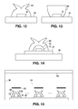
- Fig. 12 is a cross-sectional view of LED 10, submount 24, and a molded side-emitting lens 84.
- lens 84 is formed of a very flexible material, such as silicone, which flexes as it is removed from the mold. When the lens is not a simple shape, the release film 18 (Fig. 1) will typically not be used.
- Fig. 13 is a cross-sectional view of LED 10, submount 24, and a molded collimating lens 86.
- the lens 86 can be produced using a deformable mold or by using a soft lens material that compresses when being pulled from the mold and expands to its molded shape after being released from the mold.
- Fig. 14 illustrates how a preformed lens 88 can be affixed over a molded lambertian lens 22.
- lens 22 is formed in the previously described manner.
- Lens 22 serves to encapsulate and protect LED 10 from contaminants.
- a preformed side-emitting lens 88 is then affixed over lens 22 using a UV curable adhesive or a mechanical clamp.
- This lens-forming technique has advantages over conventional techniques.
- a preformed lens e.g., a side emitting lens
- the conventional process is difficult to perform due to, among other reasons, carefully positioning the separated die/submount for the lens placement and gap-filling steps.
- a large array of LEDs (Fig. 4) can be encapsulated simultaneously by forming a molded lens over each. Then, a preformed lens 88 can be affixed over each molded lens 22 while the LEDs are still in the array (Fig. 4) or after being separated.
- the molded lens can be made very small (e.g., 1-2mm diameter), unlike a conventional lens.
- a very small, fully encapsulated LED can be formed.
- Such LEDs can be made to have a very low profile, which is beneficial for certain applications.
- Fig. 14 also shows a circuit board 45 on which submount 24 is mounted.
- This circuit board 45 may have mounted on it an array of LEDs/submounts 24.
- Fig. 15 is a cross-sectional view of a backlight for a liquid crystal display (LCD) or other display that uses a backlight.
- LCD liquid crystal display
- the LEDs may be red, green, and blue to create white light.
- the LEDs form a two-dimensional array. In the example shown, each LED structure is that shown in Fig. 14, but any suitable lens may be used.
- the bottom and sidewalls 90 of the backlight box are preferably coated with a white reflectively diffusing material. Directly above each LED is a white diffuser dot 92 to prevent spots of light from being emitted by the backlight directly above each LED.
- the dots 92 are supported by a transparent or diffusing PMMA sheet 94.
- the light emitted by the side-emitting lenses 88 is mixed in the lower portion of the backlight, then further mixed in the upper portion of the backlight before exiting the upper diffuser 96.
- Linear arrays of LEDs may be mounted on narrow circuits boards 45.
- Fig. 16 illustrates an LED 10 with a molded lens 22 being used as a flash in a camera.
- the camera in Fig. 16 is part of a cellular telephone 98.
- the cellular telephone 98 includes a color screen 100 (which may have a backlight using the LEDs described herein) and a keypad 102.
- an outer lens may be formed over the inner shell to further shape the beam.
- Different shell materials may be used, depending on the requirements of the various shells.
- Figs. 17-30 illustrate examples of various lenses and materials that may be used in conjunction with the over molding process.
- Figs. 17 and 18 illustrate two shapes of molded lenses for an inner shell formed using the molding techniques described above.
- Many LEDs 10 may be mounted on the same support structure 12.
- the support structure 12 may be a ceramic or silicon submount with metal traces and contact pads, as previously described. Any number of LEDs may be mounted on the same support structure 12, and all LEDs on the same support structure 12 would typically be processed in an identical manner, although not necessarily. For example, if the support structure were large and the light pattern for the entire LED array were specified, each LED lens may differ to provide the specified overall light pattern.
- An under fill material may be injected to fill any gap between the bottom of the LED die 10 and the support substrate 12 to prevent any air gaps under the LED and to improve heat conduction, among other things.
- Fig. 17 has been described above with respect to Figs. 3-6, where the inner molded lens 22 is generally hemispherical for a lambertian radiation pattern.
- the inner molded lens 106 in Fig. 18 is generally rectangular with rounded edges.
- one of the inner molded lenses 22 or 106 may be more suitable.
- Other shapes of inner molded lenses may also be suitable.
- the top down view of each lens will generally be circular.
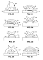
- Fig. 19 illustrates the structure of Fig. 18 with the lens outer surface having a pattern that refracts light to achieve a desired radiation pattern.
- the outer surface pattern may be directly formed in the inner molded lens (by the mold itself), or the outer surface pattern may be formed in an outer lens that is over molded onto the inner molded lens or is affixed to it by an adhesive (e.g., silicone, epoxy, etc.).
- Pattern 108 is a diffraction grating, while pattern 110 uses binary steps to refract the light.
- the pattern forms a generally side-emitting lens with the radiation pattern shown in Fig. 20.
- the peak intensity occurs within 50-80 degrees and is significantly greater than the intensity at 0 degrees.
- the requirements for the inner lens are generally different from the requirements for the outer lens.
- the inner lens should have good adhesion to the support structure, not yellow or become more opaque over time, have a high index of refraction (greater than 1.4), not break or stress any wires to the LED, withstand the high LED temperatures, and have a compatible thermal coefficient.
- the inner lens should be non-rigid (e.g., silicone) to not provide stress on the LED or any wires.
- the outer lens material generally only needs to be able to be patterned with the desired pattern and adhere to the inner lens.
- the outer lens may over molded or may be preformed and adhesively affixed to the inner lens.
- the material for the outer lens may be UV curable, while the material for the inner lens may be thermally cured. Thermal curing takes longer than UV curing.
- the range of hardness for the inner lens material is Shore 00 5-90, while the range of hardness for the outer shell(s) is Shore A 30 or more.
- Fig. 21 illustrates a Fresnel lens pattern 112 formed on the outer surface of the lens for creating a generally side-emitting light pattern similar to that of Fig. 20.
- the outer surface may be the outer surface of the inner molded lens or the outer surface of an outer shell, as described with respect to Fig. 19. This applies to all patterns described herein.
- Fig. 22 illustrates pyramid 114 or cone shaped 116 patterns on the outer lens surface to create a collimating light pattern or another light pattern.
- Fig. 23 illustrates a high dome outer lens 118 for creating a collimating pattern.
- the surface patterns of Figs. 19 and 21-23 may be configured (e.g., by changing the surface angles) to create any light pattern. Holographic structures, TIR, and other patterns may be formed. Collimating light patterns are typically used for rear projection TVs, while side-emitting light patterns are typically used for backlighting LCD screens.
- Fig. 24 illustrates the use of a soft (e.g., Shore XX) material, such as a silicone gel, as the inner molded lens 124 so as to not stress the wire 126 bonded to the LED 10.
- the gel is typically UV cured.
- the outer lens 128 may be molded or preformed and affixed with an adhesive. The outer lens 128 will typically be much harder for durability, resistance to particles, etc.
- the outer lens 128 may be silicone, epoxy-silicone, epoxy, silicone elastomers, hard rubber, other polymers, or other material.
- the outer lens may be UV or thermally cured.
- Fig. 25 is similar to Fig. 24 but with a different shaped inner molded lens 129 (like Fig. 18) for a different emission pattern or a lower profile.
- Lens 129 may be a soft silicone gel.
- the outer lens 130 will further shape the emission pattern and protect the soft inner lens 129.
- the LEDs in all figures may be flip-chips or wire-bonded types.
- Fig. 26 illustrates an LED structure with a soft inner molded lens 132, having the properties needed for the inner lens, a hard intermediate shell 134 to act as an interface layer and for structural stability, and an outer lens 136 for creating a side-emitting light pattern.
- the outer lens 136 may be soft to facilitate the molding process.
- the outer lens 136 may be preformed and adhesively affixed to the intermediate shell 134.
- the use of the intermediate shell 134 makes the choice of the outer lens material essentially independent of the inner lens material.
- Fig. 27 illustrates how the outer lens 138 may be formed on any portion of the intermediate shell 134 or inner lens 132.
- Fig. 28 illustrates the formation of the outer lens 142 directly on the inner lens 144 material.
- Fig. 29 illustrates another shape of side-emitting lens 145 molded over an inner lens 132.
- Lens 145 may be directly molded over LED die 10 without any inner lens.
- Fig. 30 illustrates an LED where each shell 146, 147, and 148 contains a different phosphor material, such as a red-emitting phosphor, a green-emitting phosphor, and a blue-emitting phosphor.
- the LED die 10 may emit UV.
- the gaps between phosphor particles allow the UV to pass through an inner shell to energize the phosphor in an outer shell.
- red and green phosphor shells are used, and the LED die 10 emits blue light.
- the combination of red, green, and blue light create white light.
- the thickness of the shells, the density of the phosphor particles, and the order of the phosphor colors, among other things, can be adjusted to obtain the desired light. Any shape of lenses may be used.
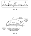
- Fig. 31 illustrates the use of a mold pattern 149 on the support structure 12 itself.
- a high index material e.g., a polymer
- a reflective material e.g., aluminum or silver
- the mold pattern 149 is then used as a mold for another material forming a lens 150.
- the lens 150 material is a liquid (e.g., silicone) that is deposited in the mold formed on the support structure 12, then cured. The surface may then be planarized. The resulting lens collimates the light by reflecting/refracting the light impinging on the walls like a reflector cup.
- Fig. 32 illustrates a molded lens 22 with metal 151 sputtered around its side to reflect light emitted by the LED 10. The reflected light will be scattered by the LED 10 and be eventually emitted through the top opening.
- the metal 151 may be any reflective material such as aluminum or silver. The metal may instead be sputtered on the top of the lens 22 to create a side-emission pattern.
- the lens 22 may be made any shape to create the desired light emission pattern.
- Fig. 33 is a side view of a liquid crystal display (LCD) 152 with an LCD screen 154, having controllable RGB pixels, a diffuser 156, and a backlight 158 for mixing light from red, green, and blue LEDs 160 to create white light.
- the backlight 158 is a diffusively reflective box.
- the LEDs 160 have side-emitting lenses made using any of the above-described techniques.
- Fig. 34 is a side view of a rear projection television 162 with a front lens 164 for brightening the image within a specified viewing angle, a set of red, green, and blue LEDs 166, modulator/optics 170 for modulating and focusing the RGB light to produce a color TV image, and a reflector 172.
- the modulator may be an array of controllable mirrors, an LCD panel, or any other suitable device.
- the LEDs 166 have collimating lenses made using any of the above-described techniques.
Landscapes
- Physics & Mathematics (AREA)
- General Physics & Mathematics (AREA)
- Optics & Photonics (AREA)
- Engineering & Computer Science (AREA)
- Manufacturing & Machinery (AREA)
- Microelectronics & Electronic Packaging (AREA)
- Led Device Packages (AREA)
- Casting Or Compression Moulding Of Plastics Or The Like (AREA)
- Liquid Crystal (AREA)
- Diffracting Gratings Or Hologram Optical Elements (AREA)
- Moulds For Moulding Plastics Or The Like (AREA)
Abstract
Description
- This is a continuation -in part of U.S. Application Serial No. 10/990,208, filed November 15, 2004, by Grigoriy Basin et al., entitled "Molded Lens Over LED Die."
- This invention relates to light emitting diodes (LEDs) and, in particular, to a technique for forming a lens over an LED die.
- LED dies typically emit light in a lambertian pattern. It is common to use a lens over the LED die to narrow the beam or to make a side-emission pattern. A common type of lens for a surface mounted LED is preformed molded plastic, which is bonded to a package in which the LED die is mounted. One such lens is shown in U.S. Patent No. 6,274,924, assigned to Lumileds Lighting and incorporated herein by reference.
- A technique for forming a lens for surface mounted LEDs is described herein.
- One or more LED dice are mounted on a support structure. The support structure may be a ceramic substrate, a silicon substrate, or other type of support structure with the LED dice electrically connected to metal pads on the support structure. The support structure may be a submount, which is mounted on a circuit board or a heat sink in a package.
- A mold has indentations in it corresponding to the positions of the LED dice on the support structure. The indentations are filled with a liquid, optically transparent material, such as silicone, which when cured forms a hardened lens material. The shape of the indentations will be the shape of the lens. The mold and the LED dice/support structure are brought together so that each LED die resides within the liquid lens material in an associated indentation.
- The mold is then heated to cure (harden) the lens material. The mold and the support structure are then separated, leaving a complete lens over each LED die. This general process will be referred to as over molding.
- The over molding process may be repeated with different molds to create concentric or overlapping shells of lenses. Each lens may have a different property, such as containing a phosphor, being a different material, providing a different radiation pattern, having a different hardness value, having a different index of refraction, or curable by a different technique (e.g., UV vs. heat).
-
- Fig. 1 is a side view of four LED dice mounted on a support structure, such as a submount, and a mold for forming a lens around each LED die.
- Fig. 2 is a side view of the LED dice being inserted into indentations in the mold filled with a liquid lens material.
- Fig. 3 is a side view of the LED dice removed from the mold after the liquid has been cured, resulting in a lens encapsulating each LED die.
- Fig. 4 is a perspective view of an array of LED dice on a submount or circuit board with a molded lens formed over each LED die.
- Fig. 5 is a close-up side view of a flip-chip LED die mounted on a submount, which is, in turn, mounted on a circuit board, and where a molded lens is formed over the LED die.
- Fig. 6 is a close-up side view of a non-flip-chip LED die mounted on a submount, which is, in turn, mounted on a circuit board, where wires electrically connect n and p metal on the LED die to leads on the circuit board, and where a molded lens is formed over the LED die.
- Figs. 7, 8, 9, 10, and 11 are cross-sectional views of an LED die with different lenses formed over it.
- Fig. 12 is a cross-sectional view of a side-emitting lens molded onto the LED die using the inventive techniques.
- Fig. 13 is a cross-sectional view of a collimating lens molded onto the LED die using the inventive techniques.
- Fig. 14 is a cross-sectional view of a preformed side-emitting lens affixed over a lambertian lens that has been molded onto the LED die using the inventive techniques.
- Fig. 15 is a cross-sectional view of a backlight for a liquid crystal display or other type of display using the LED and side-emitting lens of Fig. 14.
- Fig. 16 is a perspective view of a cell phone with a camera that uses as a flash an LED with a molded lens.
- Figs. 17 and 18 are cross-sectional views of two types of molded lenses. All lenses shown are symmetrical about the center axis, although the invention may apply to non-symmetrical lenses as well.
- Figs. 19-22 illustrate surface features on an inner lens or an outer shell lens for obtaining a desired emission pattern.
- Fig. 23 illustrates the use of a high domed lens for a collimated emission pattern.
- Figs. 24 and 25 illustrate the use of a hard outer lens and a soft inner lens to limit the stress on a wire bond.
- Figs. 26-28 illustrate the use of an outer lens formed on various types of inner or intermediate lenses for a side-emitting pattern.
- Fig. 29 illustrates another side-emitting molded lens.
- Fig. 30 illustrates the use of molded shells, each containing a different phosphor.
- Fig. 31 illustrates forming a mold portion on the support substrate for forming a molded lens.
- Fig. 32 illustrates depositing a metal reflector over a portion of the lens for achieving a desired emission pattern.
- Fig. 33 is a side view of a liquid crystal display using LEDs with side-emitting lenses in a backlight.
- Fig. 34 is a side view of a rear projection TV using LEDs with collimating lenses as a RGB light source.
- As a preliminary matter, a conventional LED is formed on a growth substrate. In the example used, the LED is a GaN-based LED, such as an AlInGaN LED, for producing blue or UV light. Typically, a relatively thick n-type GaN layer is grown on a sapphire growth substrate using conventional techniques. The relatively thick GaN layer typically includes a low temperature nucleation layer and one or more additional layers so as to provide a low-defect lattice structure for the n-type cladding layer and active layer. One or more n-type cladding layers are then formed over the thick n-type layer, followed by an active layer, one or more p-type cladding layers, and a p-type contact layer (for metallization).
- Various techniques are used to gain electrical access to the n-layers. In a flip-chip example, portions of the p-layers and active layer are etched away to expose an n-layer for metallization. In this way the p contact and n contact are on the same side of the chip and can be directly electrically attached to the package (or submount) contact pads. Current from the n-metal contact initially flows laterally through the n-layer. In contrast, in a vertical injection (non-flip-chip) LED, an n-contact is formed on one side of the chip, and a p-contact is formed on the other side of the chip. Electrical contact to one of the p or n-contacts is typically made with a wire or a metal bridge, and the other contact is directly bonded to a package (or submount) contact pad. A flip-chip LED is used in the examples of Figs. 1-3 for simplicity.
- Examples of forming LEDs are described in U.S. Patent Nos. 6,649,440 and 6,274,399, both assigned to Lumileds Lighting and incorporated by reference.
- Optionally, a conductive substrate is bonded to the LED layers (typically to the p-layers) and the sapphire substrate is removed. One or more LED dice may be bonded to a submount, with the conductive substrate directly bonded to the submount, to be described in greater detail with respect to Figs. 5 and 6. One or more submounts may be bonded to a printed circuit board, which contains metal leads for connection to other LEDs or to a power supply. The circuit board may interconnect various LEDs in series and/or parallel.
- The particular LEDs formed and whether or not they are mounted on a submount is not important for purposes of understanding the invention.
- Fig. 1 is a side view of four
LED dice 10 mounted on asupport structure 12. The support structure may be a submount (e.g., ceramic or silicon with metal leads), a metal heat sink, a printed circuit board, or any other structure. In the present example, thesupport structure 12 is a ceramic submount with metal pads/leads. - A
mold 14 hasindentations 16 corresponding to the desired shape of a lens over each LED die 10.Mold 14 is preferably formed of a metal. A very thinnon-stick film 18, having the general shape ofmold 14, is placed overmold 14.Film 18 is of a well-known conventional material that prevents the sticking of silicone to metal. -
Film 18 is not needed if the lens material does not stick to the mold. This may be accomplished by using a non-stick mold coating, using a non-stick mold material, or using a mold process that results in a non-stick interface. Such processes may involve selecting certain process temperatures to obtain the minimum stick. By not usingfilm 18, more complex lenses can be formed. - In Fig. 2, the
mold indentions 16 have been filled with a heat-curableliquid lens material 20. Thelens material 20 may be any suitable optically transparent material such as silicone, an epoxy, or a hybrid silicone/epoxy. A hybrid may be used to achieve a matching coefficient of thermal expansion (CTE). Silicone and epoxy have a sufficiently high index of refraction (greater than 1.4) to greatly improve the light extraction from an AlInGaN or AIInGaP LED as well as act as a lens. One type of silicone has an index of refraction of 1.76. - A vacuum seal is created between the periphery of the
support structure 12 andmold 14, and the two pieces are pressed against each other so that each LED die 10 is inserted into theliquid lens material 20 and thelens material 20 is under compression. - The mold is then heated to about 150 degrees centigrade (or other suitable temperature) for a time to harden the
lens material 20. - The
support structure 12 is then separated frommold 14.Film 18 causes the resulting hardened lens to be easily released frommold 14.Film 18 is then removed. - In another embodiment, the
LED dice 10 in Fig. 1 may be first covered with a material, such as silicone or phosphor particles in a binder. The mold indentations 16 are filled with another material. When the dice are then placed in the mold, the mold material is shaped over the covering material. - Fig. 3 illustrates the resulting structure with a molded
lens 22 over each LED die 10. In one embodiment, the molded lens is between Imm and 5mm in diameter. Thelens 22 may be any size or shape. - Fig. 4 is a perspective view of a resulting structure where the
support structure 12 supports an array of LED dice, each having a moldedlens 22. The mold used would have a corresponding array of indentations. If thesupport structure 12 were a ceramic or silicon submount, each LED (with its underlying submount portion) can be separated by sawing or breaking thesubmount 12 to form individual LED dice. Alternatively, thesupport structure 12 may be separated/diced to support subgroups of LEDs or may be used without being separated/diced. - The
lens 22 not only improves the light extraction from the LED die and refracts the light to create a desired emission pattern, but the lens also encapsulates the LED die to protect the die from contaminants, add mechanical strength, and protect any wire bonds. - Fig. 5 is a simplified close-up view of one embodiment of a single flip-chip LED die 10 on a
submount 24 formed of any suitable material, such as a ceramic or silicon. In one embodiment, submount 24 acted as thesupport structure 12 in Figs. 1-4, and the die/submount of Fig. 5 was separated from the structure of Fig. 4 by sawing. The LED die 10 of Fig. 5 has a bottom p-contact layer 26, a p-metal contact 27, p-type layers 28, and a light emittingactive layer 30, n-type layers 32, and an n-metal contact 31 contacting the n-type layers 32. Metal pads onsubmount 24 are directly metal-bonded tocontacts submount 24 terminate in metal pads on the bottom surface ofsubmount 24, which are bonded to the metal leads 40 and 44 on acircuit board 45. The metal leads 40 and 44 are connected to other LEDs or to a power supply.Circuit board 45 may be a metal plate (e.g., aluminum) with the metal leads 40 and 44 overlying an insulating layer. The moldedlens 22, formed using the technique of Figs. 1-3, encapsulates the LED die 10. - The LED die 10 in Fig. 5 may also be a non-flip-chip die, with a wire connecting the top n-
layers 32 to a metal pad on thesubmount 24. Thelens 22 may encapsulate the wire. - In one embodiment, the
circuit board 45 themselves may be thesupport structure 12 of Figs. 1-3. Such an embodiment is shown in Fig. 6. Fig. 6 is a simplified close-up view of a non-flip-chip LED die 10 having a top n-metal contact 34 connected to ametal lead 40 oncircuit board 45 by awire 38. The LED die 10 is mounted on asubmount 36, which in the example of Fig. 6 is a metal slab. Awire 42 electrically connects the p-layers 26/28 to ametal lead 44 oncircuit board 45. Thelens 22 is shown completely encapsulating the wires andsubmount 36; however, in other embodiments the entire submount or the entire wire need not be encapsulated. - A common prior art encapsulation method is to spin on a protective coating. However, that encapsulation process is inappropriate for adding a phosphor coating to the LED die since the thickness of the encapsulant over the LED die is uneven. Also, such encapsulation methods do not form a lens. A common technique for providing a phosphor over the LED die is to fill a reflective cup surrounding the LED die with a silicone/phosphor composition. However, that technique forms a phosphor layer with varying thick nesses and does not form a suitable lens. If a lens is desired, additional processes still have to create a plastic molded lens and affix it over the LED die.
- Figs. 7-11 illustrate various lenses that may be formed using the above-described techniques.
- Fig. 7 illustrates an LED die 10 that has been coated with a
phosphor 60 using any suitable method. One such method is by electrophoresis, described in U.S. Patent No. 6,576,488, assigned to Lumileds Lighting and incorporated herein by reference. Suitable phosphors are well known. Alens 22 is formed using the techniques described above. Thephosphor 60 is energized by the LED emission (e.g., blue or UV light) and emits light of a different wavelength, such as green, yellow, or red. The phosphor emission alone or in conjunction with the LED emission may produce white light. - Processes for coating an LED with a phosphor are time-consuming. To eliminate the process for coating the LED die with a phosphor, the phosphor powder may be mixed with the liquid silicone so as to become embedded in the
lens 62, shown in Fig. 8. - As shown in Fig. 9, to provide a carefully controlled thickness of phosphor material over the LED die, an
inner lens 64 is formed using the above-described techniques, and a separate molding step (using a mold with deeper and wider indentations) is used to form an outer phosphor/silicone shell 66 of any thickness directly over theinner lens 64. - Fig. 10 illustrates an
outer lens 68 that may be formed over the phosphor/silicone shell 66 using another mold to further shape the beam. - Fig. 11 illustrates
shells clear silicone shells - Many other shapes of lenses can be formed using the molding technique described above. Fig. 12 is a cross-sectional view of
LED 10,submount 24, and a molded side-emittinglens 84. In one embodiment,lens 84 is formed of a very flexible material, such as silicone, which flexes as it is removed from the mold. When the lens is not a simple shape, the release film 18 (Fig. 1) will typically not be used. - Fig. 13 is a cross-sectional view of
LED 10,submount 24, and a moldedcollimating lens 86. Thelens 86 can be produced using a deformable mold or by using a soft lens material that compresses when being pulled from the mold and expands to its molded shape after being released from the mold. - Fig. 14 illustrates how a preformed
lens 88 can be affixed over a moldedlambertian lens 22. In the example of Fig. 14,lens 22 is formed in the previously described manner.Lens 22 serves to encapsulate and protectLED 10 from contaminants. A preformed side-emittinglens 88 is then affixed overlens 22 using a UV curable adhesive or a mechanical clamp. This lens-forming technique has advantages over conventional techniques. In a conventional technique, a preformed lens (e.g., a side emitting lens) is adhesively affixed over the LED die, and any gaps are filled in by injecting silicone. The conventional process is difficult to perform due to, among other reasons, carefully positioning the separated die/submount for the lens placement and gap-filling steps. Using the inventive technique of Fig. 14, a large array of LEDs (Fig. 4) can be encapsulated simultaneously by forming a molded lens over each. Then, a preformedlens 88 can be affixed over each moldedlens 22 while the LEDs are still in the array (Fig. 4) or after being separated. - Additionally, the molded lens can be made very small (e.g., 1-2mm diameter), unlike a conventional lens. Thus, a very small, fully encapsulated LED can be formed. Such LEDs can be made to have a very low profile, which is beneficial for certain applications.
- Fig. 14 also shows a
circuit board 45 on which submount 24 is mounted. Thiscircuit board 45 may have mounted on it an array of LEDs/submounts 24. - Fig. 15 is a cross-sectional view of a backlight for a liquid crystal display (LCD) or other display that uses a backlight. Common uses are for televisions, monitors, cellular phones, etc. The LEDs may be red, green, and blue to create white light. The LEDs form a two-dimensional array. In the example shown, each LED structure is that shown in Fig. 14, but any suitable lens may be used. The bottom and sidewalls 90 of the backlight box are preferably coated with a white reflectively diffusing material. Directly above each LED is a
white diffuser dot 92 to prevent spots of light from being emitted by the backlight directly above each LED. Thedots 92 are supported by a transparent or diffusingPMMA sheet 94. The light emitted by the side-emittinglenses 88 is mixed in the lower portion of the backlight, then further mixed in the upper portion of the backlight before exiting theupper diffuser 96. Linear arrays of LEDs may be mounted onnarrow circuits boards 45. - Fig. 16 illustrates an
LED 10 with a moldedlens 22 being used as a flash in a camera. The camera in Fig. 16 is part of acellular telephone 98. Thecellular telephone 98 includes a color screen 100 (which may have a backlight using the LEDs described herein) and akeypad 102. - As discussed with respect to Fig. 10, an outer lens may be formed over the inner shell to further shape the beam. Different shell materials may be used, depending on the requirements of the various shells. Figs. 17-30 illustrate examples of various lenses and materials that may be used in conjunction with the over molding process.
- Figs. 17 and 18 illustrate two shapes of molded lenses for an inner shell formed using the molding techniques described above.
Many LEDs 10 may be mounted on thesame support structure 12. Thesupport structure 12 may be a ceramic or silicon submount with metal traces and contact pads, as previously described. Any number of LEDs may be mounted on thesame support structure 12, and all LEDs on thesame support structure 12 would typically be processed in an identical manner, although not necessarily. For example, if the support structure were large and the light pattern for the entire LED array were specified, each LED lens may differ to provide the specified overall light pattern. An under fill material may be injected to fill any gap between the bottom of the LED die 10 and thesupport substrate 12 to prevent any air gaps under the LED and to improve heat conduction, among other things. - Fig. 17 has been described above with respect to Figs. 3-6, where the inner molded
lens 22 is generally hemispherical for a lambertian radiation pattern. The inner moldedlens 106 in Fig. 18 is generally rectangular with rounded edges. Depending on the radiation pattern to be provided by an outer lens, one of the inner moldedlenses - Fig. 19 illustrates the structure of Fig. 18 with the lens outer surface having a pattern that refracts light to achieve a desired radiation pattern. The outer surface pattern may be directly formed in the inner molded lens (by the mold itself), or the outer surface pattern may be formed in an outer lens that is over molded onto the inner molded lens or is affixed to it by an adhesive (e.g., silicone, epoxy, etc.).
Pattern 108 is a diffraction grating, whilepattern 110 uses binary steps to refract the light. In the examples, the pattern forms a generally side-emitting lens with the radiation pattern shown in Fig. 20. In Fig. 20, the peak intensity occurs within 50-80 degrees and is significantly greater than the intensity at 0 degrees. - The requirements for the inner lens are generally different from the requirements for the outer lens. For example, the inner lens should have good adhesion to the support structure, not yellow or become more opaque over time, have a high index of refraction (greater than 1.4), not break or stress any wires to the LED, withstand the high LED temperatures, and have a compatible thermal coefficient. The inner lens should be non-rigid (e.g., silicone) to not provide stress on the LED or any wires. In contrast, the outer lens material generally only needs to be able to be patterned with the desired pattern and adhere to the inner lens. The outer lens may over molded or may be preformed and adhesively affixed to the inner lens. The material for the outer lens may be UV curable, while the material for the inner lens may be thermally cured. Thermal curing takes longer than UV curing.
- Generally, the range of hardness for the inner lens material is Shore 00 5-90, while the range of hardness for the outer shell(s) is
Shore A 30 or more. - Fig. 21 illustrates a
Fresnel lens pattern 112 formed on the outer surface of the lens for creating a generally side-emitting light pattern similar to that of Fig. 20. The outer surface may be the outer surface of the inner molded lens or the outer surface of an outer shell, as described with respect to Fig. 19. This applies to all patterns described herein. - Fig. 22 illustrates
pyramid 114 or cone shaped 116 patterns on the outer lens surface to create a collimating light pattern or another light pattern. - Fig. 23 illustrates a high dome
outer lens 118 for creating a collimating pattern. - The surface patterns of Figs. 19 and 21-23 may be configured (e.g., by changing the surface angles) to create any light pattern. Holographic structures, TIR, and other patterns may be formed. Collimating light patterns are typically used for rear projection TVs, while side-emitting light patterns are typically used for backlighting LCD screens.
- Fig. 24 illustrates the use of a soft (e.g., Shore XX) material, such as a silicone gel, as the inner molded
lens 124 so as to not stress thewire 126 bonded to theLED 10. The gel is typically UV cured. Theouter lens 128 may be molded or preformed and affixed with an adhesive. Theouter lens 128 will typically be much harder for durability, resistance to particles, etc. Theouter lens 128 may be silicone, epoxy-silicone, epoxy, silicone elastomers, hard rubber, other polymers, or other material. The outer lens may be UV or thermally cured. - Fig. 25 is similar to Fig. 24 but with a different shaped inner molded lens 129 (like Fig. 18) for a different emission pattern or a lower profile.
Lens 129 may be a soft silicone gel. Theouter lens 130 will further shape the emission pattern and protect the softinner lens 129. - The LEDs in all figures may be flip-chips or wire-bonded types.
- Fig. 26 illustrates an LED structure with a soft inner molded
lens 132, having the properties needed for the inner lens, a hardintermediate shell 134 to act as an interface layer and for structural stability, and anouter lens 136 for creating a side-emitting light pattern. Theouter lens 136 may be soft to facilitate the molding process. Alternatively, theouter lens 136 may be preformed and adhesively affixed to theintermediate shell 134. The use of theintermediate shell 134 makes the choice of the outer lens material essentially independent of the inner lens material. - Fig. 27 illustrates how the
outer lens 138 may be formed on any portion of theintermediate shell 134 orinner lens 132. - Fig. 28 illustrates the formation of the
outer lens 142 directly on theinner lens 144 material. - Fig. 29 illustrates another shape of side-emitting
lens 145 molded over aninner lens 132.Lens 145 may be directly molded over LED die 10 without any inner lens. - Fig. 30 illustrates an LED where each
shell - Fig. 31 illustrates the use of a
mold pattern 149 on thesupport structure 12 itself. A high index material (e.g., a polymer) or a reflective material (e.g., aluminum or silver) is formed by either molding the pattern on thesupport structure 12, using a method similar to the method shown in Fig. 1, or using a metallization process, or using another suitable process. Themold pattern 149 is then used as a mold for another material forming alens 150. In one embodiment, thelens 150 material is a liquid (e.g., silicone) that is deposited in the mold formed on thesupport structure 12, then cured. The surface may then be planarized. The resulting lens collimates the light by reflecting/refracting the light impinging on the walls like a reflector cup. - Fig. 32 illustrates a molded
lens 22 withmetal 151 sputtered around its side to reflect light emitted by theLED 10. The reflected light will be scattered by theLED 10 and be eventually emitted through the top opening. Themetal 151 may be any reflective material such as aluminum or silver. The metal may instead be sputtered on the top of thelens 22 to create a side-emission pattern. Thelens 22 may be made any shape to create the desired light emission pattern. - Fig. 33 is a side view of a liquid crystal display (LCD) 152 with an
LCD screen 154, having controllable RGB pixels, a diffuser 156, and abacklight 158 for mixing light from red, green, andblue LEDs 160 to create white light. Thebacklight 158 is a diffusively reflective box. TheLEDs 160 have side-emitting lenses made using any of the above-described techniques. - Fig. 34 is a side view of a
rear projection television 162 with afront lens 164 for brightening the image within a specified viewing angle, a set of red, green, andblue LEDs 166, modulator/optics 170 for modulating and focusing the RGB light to produce a color TV image, and areflector 172. The modulator may be an array of controllable mirrors, an LCD panel, or any other suitable device. TheLEDs 166 have collimating lenses made using any of the above-described techniques. - While particular embodiments of the present invention have been shown and described, it will be obvious to those skilled in the art that changes and modifications may be made without departing from this invention in its broader aspects and, therefore, the appended claims are to encompass within their scope all such changes and modifications as fall within the true spirit and scope of this invention.
Claims (36)
- A method for forming a lens over a light emitting diode (LED) die comprising:providing an LED die attached to a support structure; andmolding a first lens of a first material over the die while attached to the support structure.
- The method of Claim 1 wherein molding the first lens further comprises curing the first material using a thermal or UV cure.
- The method of Claim 1 wherein molding the first lens comprises:filling a first indentation in a first mold with a first lens material;bringing the first mold and the support structure together so that the LED die is within the first lens material;curing the liquid first lens material; andremoving the support structure from the first mold so that a first lens formed from the cured first lens material overlies the LED die.
- The method of Claim 1 wherein the support structure comprises a submount having metal leads in electrical contact with metal contacts on the LED die.
- The method of Claim 1 wherein the LED die is one of a plurality of LED dice affixed to the support structure.
- The method of Claim 1 wherein the first lens is formed in direct contact with the LED die.
- The method of Claim 1 wherein molding the first lens further comprises molding a pattern into a surface of the first lens for affecting an emitted light pattern.
- The method of 7 wherein the pattern comprises a Fresnel lens, a diffraction grating, a binary pattern, pyramids, or cones.
- The method of Claim 1 further comprising providing an optical element affixed to the first lens to obtain a desired light pattern.
- The method of Claim 9 wherein the optical element comprises a second lens of a second material different from the first material.
- The method of Claim 9 wherein the optical element comprises a second lens of a second material different from the first material, and wherein providing the optical element comprises:molding the second lens over the first lens; andcuring the second material.
- The method of Claim 9 wherein the optical element comprises a second lens of a second material different from the first material, and wherein providing the optical element comprises:molding the second lens over the first lens, the second lens having a surface pattern comprising a Fresnel lens, a diffraction gradient, a binary pattern, pyramids, or cones.
- The method of Claim 9 wherein the optical element comprises a second lens of a second material harder than the first material.
- The method of Claim 10 wherein a range of hardness of the first lens is Shore 00 5-90, and the hardness of the second lens is greater than Shore A 30.
- The method of Claim 9 wherein providing the optical element comprises depositing a reflective material on an outer surface of the first lens.
- The method of Claim 9 wherein the optical element is a collimating lens.
- The method of Claim 9 wherein the optical element is a side-emitting lens.
- The method of Claim 9 wherein the optical element comprises a second lens of a second material different from the first material, wherein the first material and the second material comprise silicone, epoxy, or a silicone/epoxy hybrid.
- The method of Claim 9 wherein providing the optical element comprises:providing a second mold having a second indentation filled with a second lens material;bringing together the second mold and the support structure, having attached to it the LED die having the first lens, so that the first lens is within the second lens material in the second indentation;curing the second lens material; andremoving the support structure from the second mold so that the second lens material forms a first shell over the first lens.
- The method of Claim 9 wherein providing the optical element comprises providing an optical element directly on the first lens.
- The method of Claim 9 wherein the optical element comprises a second lens over the first lens, the first lens containing a first phosphor, and the second lens containing a second phosphor.
- The method of Claim 21 wherein a combination of the LED light and the light emitted by the phosphors creates white light.
- The method of Claim 9 wherein the optical element comprises a second lens over the first lens, the method further comprising molding a third lens over the second lens, the first lens containing a first phosphor, the second lens containing a second phosphor, and the third lens containing a third phosphor.
- A method for forming a lens over a light emitting diode (LED) die comprising:providing an LED die attached to a support structure;forming a mold on the support structure; andmolding a first lens of a first material over the die while attached to the support structure, using the mold on the support structure to define the shape of the first lens.
- The method of Claim 24 wherein molding the first lens comprises depositing a lens material in the mold on the support structure and then curing the lens material.
- A light emitting device comprising:a light emitting diode (LED) die attached to a support structure; anda first lens molded over the LED die and encapsulating the LED die.
- The device of Claim 26 further comprising an optical element affixed to the first lens to obtain a desired light pattern.
- The device of Claim 27 wherein the optical element comprises a second lens of a second material different from the first material.
- The device of Claim 28 wherein the second lens is molded over the first lens.
- The device of Claim 28 wherein the second lens has a pattern molded into its surface for affecting an emitted light pattern.
- The device of Claim 30 wherein the pattern comprises a Fresnel lens, a diffraction grating, a binary pattern, pyramids, or cones.
- The device of Claim 26 wherein the first lens has a pattern molded into its surface for affecting an emitted light pattern.
- The device of Claim 32 wherein the pattern comprises a Fresnel lens, a diffraction grating, a binary pattern, pyramids, or cones.
- The device of Claim 26 wherein the LED die is one of a plurality of LED dice affixed to the support structure.
- The device of Claim 26 further comprising a backlight for a liquid crystal display, the backlight incorporating the LED and first lens.
- The device of Claim 26 further comprising a rear projection television, the television incorporating the LED and first lens.
Priority Applications (2)
| Application Number | Priority Date | Filing Date | Title |
|---|---|---|---|
| EP12152678.4A EP2448022A3 (en) | 2004-11-15 | 2005-11-14 | Molding a lens over a LED die |
| EP12152659.4A EP2448021A3 (en) | 2004-11-15 | 2005-11-14 | Molding a lens over a LED die |
Applications Claiming Priority (2)
| Application Number | Priority Date | Filing Date | Title |
|---|---|---|---|
| US10/990,208 US7452737B2 (en) | 2004-11-15 | 2004-11-15 | Molded lens over LED die |
| US11/069,418 US7344902B2 (en) | 2004-11-15 | 2005-02-28 | Overmolded lens over LED die |
Related Child Applications (2)
| Application Number | Title | Priority Date | Filing Date |
|---|---|---|---|
| EP12152659.4A Division-Into EP2448021A3 (en) | 2004-11-15 | 2005-11-14 | Molding a lens over a LED die |
| EP12152678.4A Division-Into EP2448022A3 (en) | 2004-11-15 | 2005-11-14 | Molding a lens over a LED die |
Publications (3)
| Publication Number | Publication Date |
|---|---|
| EP1657758A2 true EP1657758A2 (en) | 2006-05-17 |
| EP1657758A3 EP1657758A3 (en) | 2011-03-23 |
| EP1657758B1 EP1657758B1 (en) | 2015-03-25 |
Family
ID=35709271
Family Applications (3)
| Application Number | Title | Priority Date | Filing Date |
|---|---|---|---|
| EP12152659.4A Withdrawn EP2448021A3 (en) | 2004-11-15 | 2005-11-14 | Molding a lens over a LED die |
| EP12152678.4A Withdrawn EP2448022A3 (en) | 2004-11-15 | 2005-11-14 | Molding a lens over a LED die |
| EP05110719.1A Expired - Lifetime EP1657758B1 (en) | 2004-11-15 | 2005-11-14 | Method of manufacturing a light emitting diode with molded lens |
Family Applications Before (2)
| Application Number | Title | Priority Date | Filing Date |
|---|---|---|---|
| EP12152659.4A Withdrawn EP2448021A3 (en) | 2004-11-15 | 2005-11-14 | Molding a lens over a LED die |
| EP12152678.4A Withdrawn EP2448022A3 (en) | 2004-11-15 | 2005-11-14 | Molding a lens over a LED die |
Country Status (4)
| Country | Link |
|---|---|
| US (2) | US7344902B2 (en) |
| EP (3) | EP2448021A3 (en) |
| JP (4) | JP5646799B2 (en) |
| TW (1) | TWI408835B (en) |
Cited By (48)
| Publication number | Priority date | Publication date | Assignee | Title |
|---|---|---|---|---|
| WO2007072268A1 (en) * | 2005-12-19 | 2007-06-28 | Koninklijke Philips Electronics N.V. | Side emitting light -emitting device |
| WO2008011377A3 (en) * | 2006-07-17 | 2008-03-13 | 3M Innovative Properties Co | Led package with converging extractor |
| WO2008040298A1 (en) * | 2006-09-29 | 2008-04-10 | Osram Opto Semiconductors Gmbh | Optoelectronic component |
| DE102006050880A1 (en) * | 2006-06-30 | 2008-04-17 | Osram Opto Semiconductors Gmbh | Opto-electronic component and illumination device |
| WO2008120134A1 (en) * | 2007-03-29 | 2008-10-09 | Koninklijke Philips Electronics N.V. | Light-emitting device comprising an elastomeric layer |
| DE102007025749A1 (en) * | 2007-06-01 | 2008-12-11 | Wacker Chemie Ag | Illuminant-silicone mold part |
| WO2008152610A3 (en) * | 2007-06-14 | 2009-02-05 | Philips Lumileds Lighting Co | Thin flash or video recording light using low profile side emitting led |
| EP2040316A1 (en) | 2007-09-20 | 2009-03-25 | OSRAM Opto Semiconductors GmbH | Method for manufacturing an opto-electronic component and opto-electronic component |
| WO2009066099A1 (en) * | 2007-11-19 | 2009-05-28 | Wang Nang Wang | Led chip thermal management and fabrication methods |
| WO2009103285A1 (en) * | 2008-02-22 | 2009-08-27 | Osram Opto Semiconductors Gmbh | Optoelectronic component |
| DE102008009808A1 (en) * | 2008-02-19 | 2009-08-27 | Lighting Innovation Group Ag | LED-light strip, has casting compound presented as contoured casting compound, where process of electromagnetic shaft is determined by contoured casting compound, and LED air-tightly locked by compound compared to substrate or plate |
| WO2009143796A3 (en) * | 2008-05-28 | 2010-03-11 | Osram Opto Semiconductors Gmbh | Optoelectronic semiconductor component and printed circuit board |
| WO2010052621A1 (en) * | 2008-11-05 | 2010-05-14 | Philips Lumileds Lighting Company, Llc | Overmolded phosphor lens for an led |
| EP2232592A4 (en) * | 2007-12-12 | 2011-03-02 | Innotec Corp | OVERMOLDED CIRCUIT BOARD AND METHOD |
| EP2345078A1 (en) * | 2008-10-24 | 2011-07-20 | Cree, Inc. | Lighting device using solid state light emitting devices having a transparent heat sink |
| US8039856B2 (en) | 2006-07-24 | 2011-10-18 | Samsung Led Co., Ltd. | Light emitting diode module for line light source |
| DE102010044471A1 (en) | 2010-09-06 | 2012-03-08 | Heraeus Noblelight Gmbh | Method for coating optoelectronic chip-on-board module for, e.g. high-power UV LED lamp, involves immersing optoelectronic component in carrier into silicone material, and curing and thermally cross-linking silicone material with carrier |
| WO2012031703A1 (en) | 2010-09-06 | 2012-03-15 | Heraeus Noblelight Gmbh | Coating method for an optoelectronic chip-on-board module |
| WO2012034812A3 (en) * | 2010-09-14 | 2012-06-21 | Osram Opto Semiconductors Gmbh | Radiation emitting component |
| WO2012084516A1 (en) * | 2010-12-21 | 2012-06-28 | Osram Opto Semiconductors Gmbh | Method for producing an optoelectronic component, and optoelectronic component |
| EP2429009A3 (en) * | 2007-09-20 | 2012-11-21 | OSRAM Opto Semiconductors GmbH | Method for manufacturing an opto-electronic component and opto-electronic component |
| DE102011107892A1 (en) | 2011-07-18 | 2013-01-24 | Heraeus Noblelight Gmbh | Method for coating e.g. chip-on-board UV-LED module utilized in solar cell, involves curing and cross-linking liquid silicone with optoelectronic components and carriers, and removing carrier with hardened silicone coating from mold |
| CN102954388A (en) * | 2012-12-12 | 2013-03-06 | 陕西烽火佰鸿光电科技有限公司 | Improved LED (light emitting diode) lamp and film coating method thereof |
| US8408773B2 (en) | 2007-03-19 | 2013-04-02 | Innotec Corporation | Light for vehicles |
| WO2013061228A1 (en) * | 2011-10-28 | 2013-05-02 | Koninklijke Philips Electronics N.V. | Light emitting device with integral shaped reflector |
| US8624289B2 (en) | 2007-09-28 | 2014-01-07 | Osram Opto Semiconductors Gmbh | Optoelectronic component |
| EP2031666A3 (en) * | 2007-09-03 | 2014-04-16 | Nitto Denko Corporation | Process for producing optical semiconductor device |
| US8746923B2 (en) | 2011-12-05 | 2014-06-10 | Cooledge Lighting Inc. | Control of luminous intensity distribution from an array of point light sources |
| US8764240B2 (en) | 2006-08-21 | 2014-07-01 | Innotec Corp. | Electrical device having boardless electrical component mounting arrangement |
| EP2068377A4 (en) * | 2006-09-27 | 2015-01-28 | Toshiba Kk | SEMICONDUCTOR LIGHT EMITTING DEVICE, BACKLIGHT DEVICE MADE WITH SEMICONDUCTOR LIGHT EMITTING DEVICE, AND DISPLAY DEVICE |
| US9081167B2 (en) | 2004-11-15 | 2015-07-14 | Koninklijke Philips N.V. | Lens compression molded over LED die |
| DE102015103747A1 (en) | 2015-03-13 | 2016-09-15 | Hella Kgaa Hueck & Co. | light module |
| EP3070401A1 (en) | 2015-03-13 | 2016-09-21 | Hella KGaA Hueck & Co. | Illumination device |
| EP3070396A1 (en) | 2015-03-13 | 2016-09-21 | Hella KGaA Hueck & Co. | Light module |
| WO2016156670A1 (en) * | 2015-04-02 | 2016-10-06 | Tacto Tek Oy | Multi-material structure with embedded electronics |
| EP2971944A4 (en) * | 2013-03-15 | 2016-11-16 | Cree Inc | MULTI-LENS MONOBLOC OPTICAL ELEMENT AND METHOD OF MANUFACTURE |
| EP3188261A1 (en) * | 2015-12-30 | 2017-07-05 | Maven Optronics Co., Ltd. | Chip scale packaging light emitting device and manufacturing method of the same |
| KR20170080528A (en) * | 2015-12-30 | 2017-07-10 | 마븐 옵트로닉스 씨오., 엘티디. | Chip scale packaging light emitting device and manufacturing method of the same |
| EP2472610B1 (en) * | 2010-12-31 | 2018-02-14 | InterLight Optotech Corporation | Light emitting diode package and method for manufacturing same |
| EP2406833B1 (en) * | 2008-11-13 | 2018-05-02 | Maven Optronics International Limited | Phosphor-converted light emitting device |
| US9989243B2 (en) | 2013-08-21 | 2018-06-05 | Philips Lighting Holding B.V. | Textile optics—solution for robust flexible light treatment pads |
| CN105895594B (en) * | 2015-02-13 | 2019-01-04 | 台医光电科技股份有限公司 | Optical sensing module, optical sensing accessory and optical sensing device |
| US10207440B2 (en) | 2014-10-07 | 2019-02-19 | Cree, Inc. | Apparatus and method for formation of multi-region articles |
| US10400984B2 (en) | 2013-03-15 | 2019-09-03 | Cree, Inc. | LED light fixture and unitary optic member therefor |
| EP3674143A1 (en) * | 2018-12-28 | 2020-07-01 | Seat, S.A. | Illuminated emblem for a vehicle |
| EP3123531B1 (en) * | 2014-03-27 | 2022-01-05 | Tridonic GmbH & Co. KG | Led module having an integrated secondary optical unit |
| CN115377271A (en) * | 2022-09-02 | 2022-11-22 | 盐城东山精密制造有限公司 | Novel Mini-COB packaging structure and method |
| US11695093B2 (en) | 2018-11-21 | 2023-07-04 | Analog Devices, Inc. | Superlattice photodetector/light emitting diode |
Families Citing this family (318)
| Publication number | Priority date | Publication date | Assignee | Title |
|---|---|---|---|---|
| EP1620903B1 (en) * | 2003-04-30 | 2017-08-16 | Cree, Inc. | High-power solid state light emitter package |
| US7005679B2 (en) | 2003-05-01 | 2006-02-28 | Cree, Inc. | Multiple component solid state white light |
| KR100565810B1 (en) * | 2004-06-16 | 2006-03-29 | 삼성전자주식회사 | Color signal processing device and method |
| US7534633B2 (en) * | 2004-07-02 | 2009-05-19 | Cree, Inc. | LED with substrate modifications for enhanced light extraction and method of making same |
| EP1803146A2 (en) * | 2004-09-04 | 2007-07-04 | Applied Materials, Inc. | Substrate carrier having reduced height |
| US8134292B2 (en) * | 2004-10-29 | 2012-03-13 | Ledengin, Inc. | Light emitting device with a thermal insulating and refractive index matching material |
| US9929326B2 (en) | 2004-10-29 | 2018-03-27 | Ledengin, Inc. | LED package having mushroom-shaped lens with volume diffuser |
| US8816369B2 (en) | 2004-10-29 | 2014-08-26 | Led Engin, Inc. | LED packages with mushroom shaped lenses and methods of manufacturing LED light-emitting devices |
| US8324641B2 (en) | 2007-06-29 | 2012-12-04 | Ledengin, Inc. | Matrix material including an embedded dispersion of beads for a light-emitting device |
| US7858408B2 (en) * | 2004-11-15 | 2010-12-28 | Koninklijke Philips Electronics N.V. | LED with phosphor tile and overmolded phosphor in lens |
| US7352011B2 (en) * | 2004-11-15 | 2008-04-01 | Philips Lumileds Lighting Company, Llc | Wide emitting lens for LED useful for backlighting |
| US20060124941A1 (en) * | 2004-12-13 | 2006-06-15 | Lee Jae S | Thin gallium nitride light emitting diode device |
| US9070850B2 (en) * | 2007-10-31 | 2015-06-30 | Cree, Inc. | Light emitting diode package and method for fabricating same |
| US20070000849A1 (en) * | 2005-01-25 | 2007-01-04 | Daktronics, Inc. | Modular display system |
| US20080296589A1 (en) * | 2005-03-24 | 2008-12-04 | Ingo Speier | Solid-State Lighting Device Package |
| WO2006105638A1 (en) * | 2005-04-05 | 2006-10-12 | Tir Systems Ltd. | Electronic device package with an integrated evaporator |
| CN101163748B (en) * | 2005-05-26 | 2011-04-13 | 陶氏康宁公司 | Process and silicone encapsulant composition for molding small shapes |
| US9412926B2 (en) | 2005-06-10 | 2016-08-09 | Cree, Inc. | High power solid-state lamp |
| KR101133572B1 (en) * | 2005-06-21 | 2012-04-05 | 삼성전자주식회사 | A color reproduction apparatus having a plurality of color reproduction ranges and a method for processing the color signals |
| US20070039561A1 (en) * | 2005-08-12 | 2007-02-22 | Tarlton Peter B | Luminous Resilient Leash |
| KR100722590B1 (en) * | 2005-08-30 | 2007-05-28 | 삼성전기주식회사 | LED lens for backlight |
| DE102006020529A1 (en) * | 2005-08-30 | 2007-03-01 | Osram Opto Semiconductors Gmbh | Optoelectronic component has semiconductor body emitting electromagnetic radiation that passes through an optical element comprising wavelength conversion material |
| JP2007116131A (en) * | 2005-09-21 | 2007-05-10 | Sanyo Electric Co Ltd | LED light emitting device |
| KR20070033801A (en) * | 2005-09-22 | 2007-03-27 | 삼성전기주식회사 | Light emitting diode package and manufacturing method thereof |
| US7595515B2 (en) * | 2005-10-24 | 2009-09-29 | 3M Innovative Properties Company | Method of making light emitting device having a molded encapsulant |
| WO2007050484A1 (en) * | 2005-10-24 | 2007-05-03 | 3M Innovative Properties Company | Method of making light emitting device having a molded encapsulant |
| US8172097B2 (en) * | 2005-11-10 | 2012-05-08 | Daktronics, Inc. | LED display module |
| US8130175B1 (en) | 2007-04-12 | 2012-03-06 | Daktronics, Inc. | Pixel interleaving configurations for use in high definition electronic sign displays |
| US7907133B2 (en) | 2006-04-13 | 2011-03-15 | Daktronics, Inc. | Pixel interleaving configurations for use in high definition electronic sign displays |
| US7943946B2 (en) * | 2005-11-21 | 2011-05-17 | Sharp Kabushiki Kaisha | Light emitting device |
| US20070120138A1 (en) * | 2005-11-28 | 2007-05-31 | Visteon Global Technologies, Inc. | Multi-layer light emitting device with integrated thermoelectric chip |
| EP1969633B1 (en) | 2005-12-22 | 2018-08-29 | Cree, Inc. | Lighting device |
| WO2007081719A2 (en) | 2006-01-05 | 2007-07-19 | Illumitex, Inc. | Separate optical device for directing light from an led |
| KR101325792B1 (en) * | 2006-01-17 | 2013-11-04 | 다우 코닝 코포레이션 | Thermally stable transparent silicone resin compositions and methods for their preparation and use |
| KR100764148B1 (en) * | 2006-01-17 | 2007-10-05 | 루시미아 주식회사 | Sheet-like phosphor, manufacturing method thereof and light emitting device using same |
| CN101336383B (en) * | 2006-02-01 | 2012-05-09 | 陶氏康宁公司 | Impact resistant optical waveguide and method of making same |
| KR100867519B1 (en) * | 2006-02-02 | 2008-11-07 | 삼성전기주식회사 | Light emitting diode module |
| WO2007100445A2 (en) * | 2006-02-24 | 2007-09-07 | Dow Corning Corporation | Light emitting device encapsulated with silicones and curable silicone compositions for preparing the silicones |
| EP2011164B1 (en) * | 2006-04-24 | 2018-08-29 | Cree, Inc. | Side-view surface mount white led |
| KR100731678B1 (en) * | 2006-05-08 | 2007-06-22 | 서울반도체 주식회사 | Chip type light emitting diode package and light emitting device having the same |
| US7655486B2 (en) * | 2006-05-17 | 2010-02-02 | 3M Innovative Properties Company | Method of making light emitting device with multilayer silicon-containing encapsulant |
| US20070269586A1 (en) * | 2006-05-17 | 2007-11-22 | 3M Innovative Properties Company | Method of making light emitting device with silicon-containing composition |
| EP2027602A4 (en) * | 2006-05-23 | 2012-11-28 | Cree Inc | LIGHTING DEVICE AND MANUFACTURING METHOD |
| KR100789951B1 (en) * | 2006-06-09 | 2008-01-03 | 엘지전자 주식회사 | Light emitting unit manufacturing apparatus and method |
| US7906794B2 (en) | 2006-07-05 | 2011-03-15 | Koninklijke Philips Electronics N.V. | Light emitting device package with frame and optically transmissive element |
| KR20090031446A (en) * | 2006-07-06 | 2009-03-25 | 티아이알 테크놀로지 엘피 | Lighting device package |
| JP4937845B2 (en) * | 2006-08-03 | 2012-05-23 | 日立マクセル株式会社 | Illumination device and display device |
| JP2008060542A (en) * | 2006-08-03 | 2008-03-13 | Toyoda Gosei Co Ltd | LIGHT EMITTING DEVICE, LIGHT EMITTING DEVICE MANUFACTURING METHOD, AND LIGHT SOURCE DEVICE HAVING THE SAME |
| US8092735B2 (en) * | 2006-08-17 | 2012-01-10 | 3M Innovative Properties Company | Method of making a light emitting device having a molded encapsulant |
| US7763478B2 (en) | 2006-08-21 | 2010-07-27 | Cree, Inc. | Methods of forming semiconductor light emitting device packages by liquid injection molding |
| MY147460A (en) | 2006-08-28 | 2012-12-14 | Dow Corning | Optical devices and silicone compositions and process fabricating the optical devices |
| WO2008026717A1 (en) * | 2006-08-29 | 2008-03-06 | Panasonic Corporation | Electroluminescent phos phor- converted light source and method for manufacturing the same |
| KR100790741B1 (en) * | 2006-09-07 | 2008-01-02 | 삼성전기주식회사 | How to make lens for LED package |
| US20100224890A1 (en) * | 2006-09-18 | 2010-09-09 | Cree, Inc. | Light emitting diode chip with electrical insulation element |
| KR100755612B1 (en) * | 2006-09-21 | 2007-09-06 | 삼성전기주식회사 | Manufacturing method of LED package and manufacturing method of white light source module |
| US8087960B2 (en) | 2006-10-02 | 2012-01-03 | Illumitex, Inc. | LED system and method |
| KR101271225B1 (en) * | 2006-10-31 | 2013-06-03 | 삼성디스플레이 주식회사 | Method for manufacturing light emitting diode chip and light emitting diode light source module |
| CN101536179B (en) * | 2006-10-31 | 2011-05-25 | 皇家飞利浦电子股份有限公司 | Lighting device package |
| WO2008073400A1 (en) | 2006-12-11 | 2008-06-19 | The Regents Of The University Of California | Transparent light emitting diodes |
| JP5028562B2 (en) * | 2006-12-11 | 2012-09-19 | 株式会社ジャパンディスプレイイースト | LIGHTING DEVICE AND DISPLAY DEVICE USING THE LIGHTING DEVICE |
| JP2008166782A (en) * | 2006-12-26 | 2008-07-17 | Seoul Semiconductor Co Ltd | Light emitting element |
| KR101297405B1 (en) | 2006-12-26 | 2013-08-19 | 서울반도체 주식회사 | Light emitting device employing dielectric multilayer reflecting mirror |
| KR101253183B1 (en) * | 2007-01-26 | 2013-04-10 | 엘지전자 주식회사 | Printed circuit board, light emitting apparatus having the same and method for manufacturing thereof |
| SG144777A1 (en) * | 2007-01-31 | 2008-08-28 | Advanced Systems Automation | Direct molding system and process |
| US7709853B2 (en) * | 2007-02-12 | 2010-05-04 | Cree, Inc. | Packaged semiconductor light emitting devices having multiple optical elements |
| US9711703B2 (en) | 2007-02-12 | 2017-07-18 | Cree Huizhou Opto Limited | Apparatus, system and method for use in mounting electronic elements |
| US9061450B2 (en) * | 2007-02-12 | 2015-06-23 | Cree, Inc. | Methods of forming packaged semiconductor light emitting devices having front contacts by compression molding |
| US20080197369A1 (en) * | 2007-02-20 | 2008-08-21 | Cree, Inc. | Double flip semiconductor device and method for fabrication |
| US7446385B2 (en) * | 2007-03-02 | 2008-11-04 | Micron Technology, Inc. | Methods of fabricating optical packages, systems comprising the same, and their uses |
| JP2008227119A (en) * | 2007-03-13 | 2008-09-25 | Shin Etsu Chem Co Ltd | Integrated structure of light-emitting diode chip and lens and method for manufacturing the same |
| JP5149529B2 (en) * | 2007-03-30 | 2013-02-20 | 株式会社朝日ラバー | Optical component for illumination and lighting apparatus using the same |
| DE102007017855A1 (en) * | 2007-04-16 | 2008-10-23 | Osram Opto Semiconductors Gmbh | Method for producing an optoelectronic component and optoelectronic component |
| US7964888B2 (en) * | 2007-04-18 | 2011-06-21 | Cree, Inc. | Semiconductor light emitting device packages and methods |
| US7976194B2 (en) * | 2007-05-04 | 2011-07-12 | Ruud Lighting, Inc. | Sealing and thermal accommodation arrangement in LED package/secondary lens structure |
| JP5006102B2 (en) | 2007-05-18 | 2012-08-22 | 株式会社東芝 | Light emitting device and manufacturing method thereof |
| US20090008662A1 (en) * | 2007-07-05 | 2009-01-08 | Ian Ashdown | Lighting device package |
| US8350788B1 (en) | 2007-07-06 | 2013-01-08 | Daktronics, Inc. | Louver panel for an electronic sign |
| US8791631B2 (en) | 2007-07-19 | 2014-07-29 | Quarkstar Llc | Light emitting device |
| US7863635B2 (en) * | 2007-08-07 | 2011-01-04 | Cree, Inc. | Semiconductor light emitting devices with applied wavelength conversion materials |
| US20090039375A1 (en) * | 2007-08-07 | 2009-02-12 | Cree, Inc. | Semiconductor light emitting devices with separated wavelength conversion materials and methods of forming the same |
| CN101373223B (en) * | 2007-08-20 | 2012-09-26 | 香港应用科技研究院有限公司 | Optical element and backlight module including same |
| JP2009051107A (en) * | 2007-08-28 | 2009-03-12 | Towa Corp | Optical element resin sealing molding method and apparatus |
| JP5044329B2 (en) * | 2007-08-31 | 2012-10-10 | 株式会社東芝 | Light emitting device |
| TW200910648A (en) | 2007-08-31 | 2009-03-01 | Isotech Products Inc | Forming process of resin lens of an LED component |
| US20090065792A1 (en) * | 2007-09-07 | 2009-03-12 | 3M Innovative Properties Company | Method of making an led device having a dome lens |
| TW200915599A (en) * | 2007-09-17 | 2009-04-01 | Helio Optoelectronics Corp | Manufacturing method of LED having multi-layered optical lens, and structure thereof |
| WO2009039680A1 (en) * | 2007-09-27 | 2009-04-02 | Helio Optoelectronics Corporation | Manufacturing method of led having multi-layer lenses and the structure thereof |
| JP2009094199A (en) * | 2007-10-05 | 2009-04-30 | Sharp Corp | Light emitting device, surface light source, display device, and manufacturing method thereof |
| JP5262054B2 (en) * | 2007-10-10 | 2013-08-14 | 日亜化学工業株式会社 | Method for manufacturing light emitting device |
| KR101525274B1 (en) * | 2007-10-26 | 2015-06-02 | 크리, 인코포레이티드 | Illumination device having one or more lumiphors, and methods of fabricating same |
| US10256385B2 (en) | 2007-10-31 | 2019-04-09 | Cree, Inc. | Light emitting die (LED) packages and related methods |
| US9666762B2 (en) * | 2007-10-31 | 2017-05-30 | Cree, Inc. | Multi-chip light emitter packages and related methods |
| US9431589B2 (en) * | 2007-12-14 | 2016-08-30 | Cree, Inc. | Textured encapsulant surface in LED packages |
| US10008637B2 (en) | 2011-12-06 | 2018-06-26 | Cree, Inc. | Light emitter devices and methods with reduced dimensions and improved light output |
| JP2011512037A (en) | 2008-02-08 | 2011-04-14 | イルミテックス, インコーポレイテッド | System and method for emitter layer shaping |
| US20090230409A1 (en) * | 2008-03-17 | 2009-09-17 | Philips Lumileds Lighting Company, Llc | Underfill process for flip-chip leds |
| JP2009252781A (en) * | 2008-04-01 | 2009-10-29 | Shin Etsu Chem Co Ltd | Method of manufacturing resin sealed light emitting diode |
| US7841734B2 (en) * | 2008-05-27 | 2010-11-30 | Ruud Lighting, Inc. | LED lighting fixture |
| JP5427174B2 (en) * | 2008-06-23 | 2014-02-26 | パナソニック株式会社 | Light emitting device, surface light emitting device, and display device |
| US8105853B2 (en) * | 2008-06-27 | 2012-01-31 | Bridgelux, Inc. | Surface-textured encapsulations for use with light emitting diodes |
| TWI357164B (en) * | 2008-06-30 | 2012-01-21 | E Pin Optical Industry Co Ltd | Aspherical led angular lens for narrow distributio |
| TW201000602A (en) * | 2008-06-30 | 2010-01-01 | Paragon Technologies Co Ltd | Organic membrane for transmitting optical spectrum and LED chip package module |
| TWI361261B (en) * | 2008-06-30 | 2012-04-01 | E Pin Optical Industry Co Ltd | Aspherical led angular lens for wide distribution patterns and led assembly using the same |
| TWI395908B (en) * | 2008-06-30 | 2013-05-11 | E Pin Optical Industry Co Ltd | Aspherical positive-angle light-emitting diode optical lens and light-emitting diode assembly thereof |
| JP2010027974A (en) * | 2008-07-23 | 2010-02-04 | Sharp Corp | Method of manufacturing light-emitting device |
| WO2010021346A1 (en) * | 2008-08-20 | 2010-02-25 | 三菱化学株式会社 | Semiconductor light emitting device and method for manufacturing the same |
| KR100993317B1 (en) * | 2008-08-26 | 2010-11-09 | 삼성전기주식회사 | Lens manufacturing method of light emitting diode package |
| US8403538B2 (en) * | 2008-09-30 | 2013-03-26 | Tyco Electronics Corporation | Color homogenizing optical assembly |
| GB2464102A (en) * | 2008-10-01 | 2010-04-07 | Optovate Ltd | Illumination apparatus comprising multiple monolithic subarrays |
| US8944626B2 (en) | 2008-10-09 | 2015-02-03 | Surefire, Llc | Lighting device with switchable light sources |
| US8182109B2 (en) * | 2008-10-09 | 2012-05-22 | Surefire, Llc | Lighting device with switchable light sources |
| US8147089B2 (en) * | 2008-10-09 | 2012-04-03 | Surefire, Llc | Switchable light sources |
| US8534890B2 (en) * | 2008-10-09 | 2013-09-17 | Tyco Electronics Canada Ulc | Light pipe assembly having optical concentrator |
| US8075165B2 (en) | 2008-10-14 | 2011-12-13 | Ledengin, Inc. | Total internal reflection lens and mechanical retention and locating device |
| JP2010103522A (en) * | 2008-10-21 | 2010-05-06 | Seoul Opto Devices Co Ltd | Ac drive type light-emitting element with delay phosphor and light-emitting element module |
| DE102008057140A1 (en) * | 2008-11-13 | 2010-05-20 | Osram Opto Semiconductors Gmbh | Optoelectronic component |
| KR101018153B1 (en) * | 2008-11-27 | 2011-02-28 | 삼성엘이디 주식회사 | LED Package |
| US7841747B2 (en) * | 2008-12-11 | 2010-11-30 | Avago Technologies Ecbu Ip (Singapore) Pte. Ltd. | Light emitting device |
| TW201034256A (en) | 2008-12-11 | 2010-09-16 | Illumitex Inc | Systems and methods for packaging light-emitting diode devices |
| US8507300B2 (en) * | 2008-12-24 | 2013-08-13 | Ledengin, Inc. | Light-emitting diode with light-conversion layer |
| US8368112B2 (en) | 2009-01-14 | 2013-02-05 | Cree Huizhou Opto Limited | Aligned multiple emitter package |
| DE102009005907A1 (en) * | 2009-01-23 | 2010-07-29 | Osram Opto Semiconductors Gmbh | Optoelectronic semiconductor device |
| JP5428358B2 (en) * | 2009-01-30 | 2014-02-26 | ソニー株式会社 | Method for manufacturing optical element package |
| JP5327042B2 (en) * | 2009-03-26 | 2013-10-30 | 豊田合成株式会社 | LED lamp manufacturing method |
| US8382347B2 (en) * | 2009-04-02 | 2013-02-26 | Abl Ip Holding Llc | Light fixture |
| US8212263B2 (en) | 2009-04-03 | 2012-07-03 | Koninklijke Philips Electronics N.V. | Backlight including semiconductior light emitting devices |
| JP2010245477A (en) | 2009-04-10 | 2010-10-28 | Dow Corning Toray Co Ltd | Optical device and manufacturing method thereof |
| US20120086035A1 (en) * | 2009-05-11 | 2012-04-12 | SemiLEDs Optoelectronics Co., Ltd. | LED Device With A Light Extracting Rough Structure And Manufacturing Methods Thereof |
| US8434883B2 (en) | 2009-05-11 | 2013-05-07 | SemiOptoelectronics Co., Ltd. | LLB bulb having light extracting rough surface pattern (LERSP) and method of fabrication |
| RU2538100C2 (en) * | 2009-05-28 | 2015-01-10 | Конинклейке Филипс Электроникс Н.В. | Lighting device with housing enclosing light source |
| US20120065343A1 (en) | 2009-05-29 | 2012-03-15 | Maneesh Bahadur | Silicone Composition for Producing Transparent Silicone Materials and Optical Devices |
| US8921876B2 (en) | 2009-06-02 | 2014-12-30 | Cree, Inc. | Lighting devices with discrete lumiphor-bearing regions within or on a surface of remote elements |
| US8168998B2 (en) * | 2009-06-09 | 2012-05-01 | Koninklijke Philips Electronics N.V. | LED with remote phosphor layer and reflective submount |
| US8384114B2 (en) | 2009-06-27 | 2013-02-26 | Cooledge Lighting Inc. | High efficiency LEDs and LED lamps |
| JP5380182B2 (en) * | 2009-07-03 | 2014-01-08 | パナソニック株式会社 | Light emitting device, surface light source, and liquid crystal display device |
| US8431423B2 (en) * | 2009-07-16 | 2013-04-30 | Koninklijke Philips Electronics N.V. | Reflective substrate for LEDS |
| US8097894B2 (en) * | 2009-07-23 | 2012-01-17 | Koninklijke Philips Electronics N.V. | LED with molded reflective sidewall coating |
| US8449128B2 (en) | 2009-08-20 | 2013-05-28 | Illumitex, Inc. | System and method for a lens and phosphor layer |
| US8585253B2 (en) | 2009-08-20 | 2013-11-19 | Illumitex, Inc. | System and method for color mixing lens array |
| US20110051413A1 (en) * | 2009-08-25 | 2011-03-03 | Abl Ip Holding Llc | Optic shielding |
| US20110049545A1 (en) * | 2009-09-02 | 2011-03-03 | Koninklijke Philips Electronics N.V. | Led package with phosphor plate and reflective substrate |
| EP2481976B1 (en) * | 2009-09-25 | 2015-04-08 | Luxintec, S.L. | Optical illumination device |
| US9453994B2 (en) * | 2009-09-25 | 2016-09-27 | Osram Opto Semiconductors Gmbh | Luminaire |
| US20110089447A1 (en) * | 2009-10-19 | 2011-04-21 | Wu-Cheng Kuo | Light-emiting device chip with micro-lenses and method for fabricating the same |
| JP5637675B2 (en) * | 2009-10-29 | 2014-12-10 | 株式会社朝日ラバー | Hybrid lens |
| US8203161B2 (en) | 2009-11-23 | 2012-06-19 | Koninklijke Philips Electronics N.V. | Wavelength converted semiconductor light emitting device |
| US8465172B2 (en) * | 2009-12-17 | 2013-06-18 | Phoseon Technology, Inc. | Lighting module with diffractive optical element |
| KR101186648B1 (en) * | 2009-12-21 | 2012-09-28 | 서울반도체 주식회사 | Light emitting diode package and method for fabricating the same diode |
| US9480133B2 (en) | 2010-01-04 | 2016-10-25 | Cooledge Lighting Inc. | Light-emitting element repair in array-based lighting devices |
| US8653539B2 (en) | 2010-01-04 | 2014-02-18 | Cooledge Lighting, Inc. | Failure mitigation in arrays of light-emitting devices |
| KR20110087579A (en) * | 2010-01-26 | 2011-08-03 | 삼성엘이디 주식회사 | LED module and backlight unit having the same |
| JP5010693B2 (en) * | 2010-01-29 | 2012-08-29 | 株式会社東芝 | LED package |
| JP5623092B2 (en) * | 2010-02-04 | 2014-11-12 | 信越化学工業株式会社 | Manufacturing method of integrated structure of light emitting diode chip and lens |
| US8783915B2 (en) | 2010-02-11 | 2014-07-22 | Bridgelux, Inc. | Surface-textured encapsulations for use with light emitting diodes |
| US8771577B2 (en) * | 2010-02-16 | 2014-07-08 | Koninklijke Philips N.V. | Light emitting device with molded wavelength converting layer |
| US9500325B2 (en) | 2010-03-03 | 2016-11-22 | Cree, Inc. | LED lamp incorporating remote phosphor with heat dissipation features |
| US10359151B2 (en) | 2010-03-03 | 2019-07-23 | Ideal Industries Lighting Llc | Solid state lamp with thermal spreading elements and light directing optics |
| US9275979B2 (en) | 2010-03-03 | 2016-03-01 | Cree, Inc. | Enhanced color rendering index emitter through phosphor separation |
| US9310030B2 (en) | 2010-03-03 | 2016-04-12 | Cree, Inc. | Non-uniform diffuser to scatter light into uniform emission pattern |
| US8562161B2 (en) | 2010-03-03 | 2013-10-22 | Cree, Inc. | LED based pedestal-type lighting structure |
| US9316361B2 (en) | 2010-03-03 | 2016-04-19 | Cree, Inc. | LED lamp with remote phosphor and diffuser configuration |
| US8931933B2 (en) | 2010-03-03 | 2015-01-13 | Cree, Inc. | LED lamp with active cooling element |
| US9062830B2 (en) | 2010-03-03 | 2015-06-23 | Cree, Inc. | High efficiency solid state lamp and bulb |
| US9057511B2 (en) | 2010-03-03 | 2015-06-16 | Cree, Inc. | High efficiency solid state lamp and bulb |
| US9625105B2 (en) | 2010-03-03 | 2017-04-18 | Cree, Inc. | LED lamp with active cooling element |
| US8632196B2 (en) | 2010-03-03 | 2014-01-21 | Cree, Inc. | LED lamp incorporating remote phosphor and diffuser with heat dissipation features |
| US9024517B2 (en) | 2010-03-03 | 2015-05-05 | Cree, Inc. | LED lamp with remote phosphor and diffuser configuration utilizing red emitters |
| TWI476959B (en) * | 2010-04-11 | 2015-03-11 | 邱羅利士公司 | Method for transferring uniform fluorescent layer to an object and light structure obtained thereby |
| US8431942B2 (en) * | 2010-05-07 | 2013-04-30 | Koninklijke Philips Electronics N.V. | LED package with a rounded square lens |
| GB2507223B (en) * | 2010-06-17 | 2015-01-14 | Achrolux Inc | Light-emitting structure |
| CN102959708B (en) | 2010-06-29 | 2016-05-04 | 柯立芝照明有限公司 | Electronic device with flexible substrate |
| TW201201409A (en) * | 2010-06-29 | 2012-01-01 | Semileds Optoelectronics Co | Chip-type light emitting device having precisely coated wavelength-converting layer and packaged structure thereof |
| US8835199B2 (en) * | 2010-07-28 | 2014-09-16 | GE Lighting Solutions, LLC | Phosphor suspended in silicone, molded/formed and used in a remote phosphor configuration |
| US10451251B2 (en) | 2010-08-02 | 2019-10-22 | Ideal Industries Lighting, LLC | Solid state lamp with light directing optics and diffuser |
| TW201207324A (en) * | 2010-08-13 | 2012-02-16 | Foxsemicon Integrated Tech Inc | Lightening structure of LED light source |
| US20120056228A1 (en) * | 2010-09-07 | 2012-03-08 | Phostek, Inc. | Led chip modules, method for packaging the led chip modules, and moving fixture thereof |
| JP2012069589A (en) * | 2010-09-21 | 2012-04-05 | Toshiba Corp | Light-emitting device |
| JP5767062B2 (en) * | 2010-09-30 | 2015-08-19 | 日東電工株式会社 | Light emitting diode sealing material and method for manufacturing light emitting diode device |
| CN102447042A (en) * | 2010-10-15 | 2012-05-09 | 展晶科技(深圳)有限公司 | LED (Light Emitting Diode) package structure and process |
| TWI478400B (en) * | 2010-10-22 | 2015-03-21 | Advanced Optoelectronic Tech | Encapsulation, light-emitting diode package and method for manufacturing encapsulation |
| US8455895B2 (en) | 2010-11-08 | 2013-06-04 | Bridgelux, Inc. | LED-based light source utilizing asymmetric conductors |
| US9478719B2 (en) | 2010-11-08 | 2016-10-25 | Bridgelux, Inc. | LED-based light source utilizing asymmetric conductors |
| KR101725220B1 (en) | 2010-12-22 | 2017-04-10 | 삼성전자 주식회사 | Method of depositing phosphor on semiconductor light emitting device and an apparatus for depositing phosphor on semiconductor light emitting device |
| US8652860B2 (en) | 2011-01-09 | 2014-02-18 | Bridgelux, Inc. | Packaging photon building blocks having only top side connections in a molded interconnect structure |
| US8354684B2 (en) | 2011-01-09 | 2013-01-15 | Bridgelux, Inc. | Packaging photon building blocks having only top side connections in an interconnect structure |
| US8536605B2 (en) * | 2011-11-28 | 2013-09-17 | Bridgelux, Inc. | Micro-bead blasting process for removing a silicone flash layer |
| KR101923588B1 (en) | 2011-01-21 | 2018-11-29 | 스탠리 일렉트릭 컴퍼니, 리미티드 | Light-Emitting Device, Method for Producing The Same, and Illuminating Device |
| US9234655B2 (en) | 2011-02-07 | 2016-01-12 | Cree, Inc. | Lamp with remote LED light source and heat dissipating elements |
| US9068701B2 (en) | 2012-01-26 | 2015-06-30 | Cree, Inc. | Lamp structure with remote LED light source |
| US11251164B2 (en) | 2011-02-16 | 2022-02-15 | Creeled, Inc. | Multi-layer conversion material for down conversion in solid state lighting |
| TW201238099A (en) * | 2011-03-02 | 2012-09-16 | E Pin Optical Industry Co Ltd | LED with primary optical lens packing method and LED assembly thereof |
| KR101367378B1 (en) | 2011-03-31 | 2014-02-26 | 서울반도체 주식회사 | Light emitting device employing dielectric multilayer reflecting mirror |
| US9029887B2 (en) | 2011-04-22 | 2015-05-12 | Micron Technology, Inc. | Solid state lighting devices having improved color uniformity and associated methods |
| US9074357B2 (en) | 2011-04-25 | 2015-07-07 | Delta Faucet Company | Mounting bracket for electronic kitchen faucet |
| US8257988B1 (en) | 2011-05-17 | 2012-09-04 | Rohm And Haas Electronic Materials Llc | Method of making light emitting diodes |
| US8497519B2 (en) | 2011-05-24 | 2013-07-30 | Tsmc Solid State Lighting Ltd. | Batwing LED with remote phosphor configuration |
| USD673126S1 (en) * | 2011-07-08 | 2012-12-25 | Cree, Inc. | LED chip |
| USD691973S1 (en) | 2011-07-08 | 2013-10-22 | Cree, Inc. | Lamp packages |
| KR20140038553A (en) | 2011-07-21 | 2014-03-28 | 크리,인코포레이티드 | Light emitter device packages, components, and mehtods for improved chemical resistance and related methods |
| US10211380B2 (en) | 2011-07-21 | 2019-02-19 | Cree, Inc. | Light emitting devices and components having improved chemical resistance and related methods |
| US10686107B2 (en) | 2011-07-21 | 2020-06-16 | Cree, Inc. | Light emitter devices and components with improved chemical resistance and related methods |
| US9845943B2 (en) | 2011-07-22 | 2017-12-19 | Guardian Glass, LLC | Heat management subsystems for LED lighting systems, LED lighting systems including heat management subsystems, and/or methods of making the same |
| US20130037931A1 (en) * | 2011-08-08 | 2013-02-14 | Leo M. Higgins, III | Semiconductor package with a heat spreader and method of making |
| CN103733362B (en) | 2011-08-16 | 2017-03-29 | 三星电子株式会社 | LED component with the luminous efficacy for improving |
| US8450445B2 (en) | 2011-08-17 | 2013-05-28 | Rohm And Haas Electronic Materials Llc | Light emitting diode manufacturing method |
| US20130056749A1 (en) * | 2011-09-07 | 2013-03-07 | Michael Tischler | Broad-area lighting systems |
| US8579451B2 (en) * | 2011-09-15 | 2013-11-12 | Osram Sylvania Inc. | LED lamp |
| US8957440B2 (en) * | 2011-10-04 | 2015-02-17 | Cree, Inc. | Light emitting devices with low packaging factor |
| US9057184B2 (en) | 2011-10-19 | 2015-06-16 | Delta Faucet Company | Insulator base for electronic faucet |
| EP2587560A1 (en) * | 2011-10-26 | 2013-05-01 | Forschungsverbund Berlin e.V. | Light emitting diode |
| EP2783398B1 (en) | 2011-11-23 | 2017-10-04 | Quarkstar LLC | Light-emitting devices providing asymmetrical propagation of light |
| WO2013082537A1 (en) * | 2011-12-01 | 2013-06-06 | Quarkstar Llc | Solid-state lighting device and method of manufacturing same |
| US9496466B2 (en) | 2011-12-06 | 2016-11-15 | Cree, Inc. | Light emitter devices and methods, utilizing light emitting diodes (LEDs), for improved light extraction |
| US8907362B2 (en) | 2012-01-24 | 2014-12-09 | Cooledge Lighting Inc. | Light-emitting dies incorporating wavelength-conversion materials and related methods |
| WO2013112435A1 (en) | 2012-01-24 | 2013-08-01 | Cooledge Lighting Inc. | Light - emitting devices having discrete phosphor chips and fabrication methods |
| US8896010B2 (en) | 2012-01-24 | 2014-11-25 | Cooledge Lighting Inc. | Wafer-level flip chip device packages and related methods |
| RU2617880C2 (en) * | 2012-02-10 | 2017-04-28 | Конинклейке Филипс Н.В. | Moulded lens forming led-module of integrated circuit scale and manufacturing method thereof |
| US9240530B2 (en) * | 2012-02-13 | 2016-01-19 | Cree, Inc. | Light emitter devices having improved chemical and physical resistance and related methods |
| US9343441B2 (en) | 2012-02-13 | 2016-05-17 | Cree, Inc. | Light emitter devices having improved light output and related methods |
| EP2823515A4 (en) * | 2012-03-06 | 2015-08-19 | Soraa Inc | LIGHT EMITTING DIODE WITH LOW REFRACTIVE INDEX TO REDUCE LIGHT GUIDING EFFECTS |
| US9488359B2 (en) | 2012-03-26 | 2016-11-08 | Cree, Inc. | Passive phase change radiators for LED lamps and fixtures |
| US9897284B2 (en) | 2012-03-28 | 2018-02-20 | Ledengin, Inc. | LED-based MR16 replacement lamp |
| WO2013154602A1 (en) * | 2012-04-12 | 2013-10-17 | Saint-Gobain Performance Plastics Corporation | Method of manufacturing light emitting device |
| JP2013230618A (en) | 2012-04-27 | 2013-11-14 | Dow Corning Toray Co Ltd | Release film, compression molding method, and compression molding apparatus |
| JP5677371B2 (en) * | 2012-06-04 | 2015-02-25 | 株式会社東芝 | Light emitting device |
| US10145026B2 (en) | 2012-06-04 | 2018-12-04 | Slt Technologies, Inc. | Process for large-scale ammonothermal manufacturing of semipolar gallium nitride boules |
| US8877561B2 (en) | 2012-06-07 | 2014-11-04 | Cooledge Lighting Inc. | Methods of fabricating wafer-level flip chip device packages |
| DE112013002944T5 (en) | 2012-06-13 | 2015-02-19 | Innotec, Corp. | Flexible hollow fiber optic cable |
| USD703348S1 (en) | 2012-07-09 | 2014-04-22 | Cree, Inc. | Lamp package |
| JP6348491B2 (en) | 2012-07-20 | 2018-06-27 | コーニンクレッカ フィリップス エヌ ヴェKoninklijke Philips N.V. | LED with ceramic green phosphor and protected red phosphor layer |
| US8974077B2 (en) | 2012-07-30 | 2015-03-10 | Ultravision Technologies, Llc | Heat sink for LED light source |
| DE102012107290A1 (en) * | 2012-08-08 | 2014-02-13 | Osram Opto Semiconductors Gmbh | Optoelectronic semiconductor device, conversion agent platelets and method of making a conversion agent platelet |
| JP2014049625A (en) * | 2012-08-31 | 2014-03-17 | Panasonic Corp | Led module |
| WO2014043410A1 (en) | 2012-09-13 | 2014-03-20 | Quarkstar Llc | Light-emitting devices with reflective elements |
| EP2896079B1 (en) | 2012-09-13 | 2018-02-28 | Quarkstar LLC | Light-emitting device with remote scattering element and total internal reflection extractor element |
| US9299687B2 (en) * | 2012-10-05 | 2016-03-29 | Bridgelux, Inc. | Light-emitting assemblies comprising an array of light-emitting diodes having an optimized lens configuration |
| US9022607B2 (en) | 2012-10-18 | 2015-05-05 | Avago Technologies General Ip (Singapore) Pte. Ltd. | Leadframe-based surface mount technology segmented display design and method of manufacture |
| KR101979825B1 (en) * | 2012-11-19 | 2019-05-17 | 서울반도체 주식회사 | Light emitting device and electronic appratus comprising the same |
| WO2014080398A1 (en) * | 2012-11-26 | 2014-05-30 | Magic Lighting Optics | Outdoor lighting device |
| US8727567B1 (en) * | 2012-12-18 | 2014-05-20 | Jds Uniphase Corporation | Semiconductor light source having a reflector |
| US9761763B2 (en) | 2012-12-21 | 2017-09-12 | Soraa, Inc. | Dense-luminescent-materials-coated violet LEDs |
| TW201430400A (en) * | 2013-01-31 | 2014-08-01 | 鴻海精密工業股份有限公司 | Diffusion lens, light module, and light source |
| US9267661B1 (en) * | 2013-03-01 | 2016-02-23 | Soraa, Inc. | Apportioning optical projection paths in an LED lamp |
| US9752757B2 (en) | 2013-03-07 | 2017-09-05 | Quarkstar Llc | Light-emitting device with light guide for two way illumination |
| US9683710B2 (en) | 2013-03-07 | 2017-06-20 | Quarkstar Llc | Illumination device with multi-color light-emitting elements |
| US9470395B2 (en) | 2013-03-15 | 2016-10-18 | Abl Ip Holding Llc | Optic for a light source |
| WO2014144706A2 (en) | 2013-03-15 | 2014-09-18 | Quarkstar Llc | Color tuning of light-emitting devices |
| US9333698B2 (en) | 2013-03-15 | 2016-05-10 | Delta Faucet Company | Faucet base ring |
| US9920901B2 (en) | 2013-03-15 | 2018-03-20 | Cree, Inc. | LED lensing arrangement |
| US10807329B2 (en) | 2013-05-10 | 2020-10-20 | Abl Ip Holding Llc | Silicone optics |
| US20140338237A1 (en) * | 2013-05-20 | 2014-11-20 | Yun-Ping Chu | Vehicle sign display employing semiconductor lighting elements |
| CN104241262B (en) | 2013-06-14 | 2020-11-06 | 惠州科锐半导体照明有限公司 | Light emitting device and display device |
| WO2015008243A1 (en) * | 2013-07-19 | 2015-01-22 | Koninklijke Philips N.V. | Pc led with optical element and without substrate carrier |
| US20150028365A1 (en) * | 2013-07-24 | 2015-01-29 | Juanita N. Kurtin | Highly refractive, transparent thermal conductors for better heat dissipation and light extraction in white leds |
| JP6318495B2 (en) | 2013-08-07 | 2018-05-09 | 日亜化学工業株式会社 | Light emitting device |
| TW201506456A (en) * | 2013-08-15 | 2015-02-16 | 鴻海精密工業股份有限公司 | Lens group and light source device using the same |
| KR102299238B1 (en) * | 2014-01-08 | 2021-09-07 | 루미리즈 홀딩 비.브이. | Wavelength converted semiconductor light emitting device |
| US9343443B2 (en) | 2014-02-05 | 2016-05-17 | Cooledge Lighting, Inc. | Light-emitting dies incorporating wavelength-conversion materials and related methods |
| US9360188B2 (en) | 2014-02-20 | 2016-06-07 | Cree, Inc. | Remote phosphor element filled with transparent material and method for forming multisection optical elements |
| CN103887406B (en) * | 2014-03-14 | 2016-06-15 | 苏州晶品光电科技有限公司 | Multi-level multimedium LED encapsulating structure |
| EP3146263B1 (en) * | 2014-05-21 | 2019-09-25 | Lumileds Holding B.V. | Method of attaching a lens to a led module with high alignment accuracy |
| CN104090423B (en) * | 2014-06-23 | 2017-08-01 | 京东方科技集团股份有限公司 | Transparent display |
| US9601670B2 (en) | 2014-07-11 | 2017-03-21 | Cree, Inc. | Method to form primary optic with variable shapes and/or geometries without a substrate |
| JP2014199958A (en) * | 2014-08-01 | 2014-10-23 | 信越化学工業株式会社 | Integrated structure of light-emitting diode chip and lens, and manufacturing method thereof |
| WO2016027186A1 (en) * | 2014-08-19 | 2016-02-25 | Koninklijke Philips N.V. | Sapphire collector for reducing mechanical damage during die level laser lift-off |
| US10622522B2 (en) | 2014-09-05 | 2020-04-14 | Theodore Lowes | LED packages with chips having insulated surfaces |
| US10249599B2 (en) * | 2016-06-29 | 2019-04-02 | eLux, Inc. | Laminated printed color conversion phosphor sheets |
| US10032969B2 (en) | 2014-12-26 | 2018-07-24 | Nichia Corporation | Light emitting device |
| KR102346157B1 (en) * | 2015-03-23 | 2021-12-31 | 쑤저우 레킨 세미컨덕터 컴퍼니 리미티드 | Light emitting device package |
| JP2016200979A (en) * | 2015-04-10 | 2016-12-01 | ホーチキ株式会社 | smoke detector |
| JP6807334B2 (en) * | 2015-05-13 | 2021-01-06 | ルミレッズ ホールディング ベーフェー | Sapphire collector to reduce mechanical damage during die-level lift-off |
| KR20170003182A (en) | 2015-06-30 | 2017-01-09 | 서울반도체 주식회사 | Light emitting diode |
| US20170338387A1 (en) * | 2015-06-30 | 2017-11-23 | Seoul Semiconductor Co., Ltd. | Light emitting diode |
| JP2017098414A (en) * | 2015-11-24 | 2017-06-01 | 三星電子株式会社Samsung Electronics Co.,Ltd. | Light emitting device |
| CN106848031A (en) | 2015-12-04 | 2017-06-13 | 财团法人工业技术研究院 | Packaging structure of ultraviolet light emitting diode |
| KR20170075897A (en) | 2015-12-23 | 2017-07-04 | 삼성전자주식회사 | Light emitting diode package |
| US10403802B2 (en) | 2016-01-19 | 2019-09-03 | Mitsubishi Electric Corporation | Method for manufacturing LED display panel |
| TWI780041B (en) | 2016-02-04 | 2022-10-11 | 晶元光電股份有限公司 | Light-emitting element and the manufacturing method thereof |
| KR102407777B1 (en) * | 2016-02-04 | 2022-06-10 | 에피스타 코포레이션 | Light-emitting element and the manufacturing method thereof |
| ITUB20161150A1 (en) * | 2016-02-29 | 2017-08-29 | Osram Gmbh | PROCEDURE FOR REALIZING LIGHTING AND CORRESPONDENT DEVICES |
| EP3491679B1 (en) | 2016-07-26 | 2023-02-22 | CreeLED, Inc. | Light emitting diodes, components and related methods |
| US10230027B2 (en) * | 2016-08-05 | 2019-03-12 | Maven Optronics Co., Ltd. | Moisture-resistant chip scale packaging light-emitting device |
| CN106252495A (en) * | 2016-09-05 | 2016-12-21 | 清华大学深圳研究生院 | A kind of LED encapsulation and fluorescent material housing thereof |
| US10393363B2 (en) | 2017-04-25 | 2019-08-27 | Delta Faucet Company | Illumination device for a fluid delivery apparatus |
| KR102424005B1 (en) * | 2017-10-26 | 2022-07-25 | 에피스타 코포레이션 | Light-emitting device |
| CN107833948A (en) * | 2017-11-28 | 2018-03-23 | 西安科锐盛创新科技有限公司 | LED encapsulation structure and its method |
| CN107833947B (en) * | 2017-11-28 | 2020-12-18 | 浙江清华柔性电子技术研究院 | A kind of LED packaging method |
| CN107863440A (en) * | 2017-11-28 | 2018-03-30 | 西安科锐盛创新科技有限公司 | High luminous efficiency led |
| JP7268315B2 (en) * | 2017-12-12 | 2023-05-08 | 日本電気硝子株式会社 | WAVELENGTH CONVERSION MEMBER, MANUFACTURING METHOD THEREOF, AND LIGHT EMITTING DEVICE |
| US20190237629A1 (en) | 2018-01-26 | 2019-08-01 | Lumileds Llc | Optically transparent adhesion layer to connect noble metals to oxides |
| CN111758168B (en) * | 2018-02-19 | 2024-05-17 | 昕诺飞控股有限公司 | Sealed device with light engine |
| US11024785B2 (en) * | 2018-05-25 | 2021-06-01 | Creeled, Inc. | Light-emitting diode packages |
| USD902448S1 (en) | 2018-08-31 | 2020-11-17 | Cree, Inc. | Light emitting diode package |
| US11233183B2 (en) | 2018-08-31 | 2022-01-25 | Creeled, Inc. | Light-emitting diodes, light-emitting diode arrays and related devices |
| US11335833B2 (en) | 2018-08-31 | 2022-05-17 | Creeled, Inc. | Light-emitting diodes, light-emitting diode arrays and related devices |
| US11333320B2 (en) * | 2018-10-22 | 2022-05-17 | American Sterilizer Company | Retroreflector LED spectrum enhancement method and apparatus |
| TWI703743B (en) * | 2018-10-31 | 2020-09-01 | 億光電子工業股份有限公司 | Lighting device and lighting module |
| JP7042735B2 (en) * | 2018-12-24 | 2022-03-28 | 三菱電機株式会社 | lens |
| CN110021698B (en) * | 2019-04-25 | 2020-05-29 | 吴宇嘉 | Packaging technology of LED display screen with double-layer sealing structure |
| US11101411B2 (en) | 2019-06-26 | 2021-08-24 | Creeled, Inc. | Solid-state light emitting devices including light emitting diodes in package structures |
| JP6787515B1 (en) * | 2019-08-02 | 2020-11-18 | 日亜化学工業株式会社 | Light emitting device and surface emitting light source |
| KR20210115236A (en) * | 2020-03-12 | 2021-09-27 | 엘지이노텍 주식회사 | LED Light source module |
| US11032976B1 (en) * | 2020-03-16 | 2021-06-15 | Hgci, Inc. | Light fixture for indoor grow application and components thereof |
| KR102341319B1 (en) * | 2020-03-16 | 2021-12-21 | (주) 헥사이노힐 | Manufacture of all-in-one chip-on-board type light emitting device for low level laser therapy(LLLT) and medical light emitting device using it |
| USD933872S1 (en) | 2020-03-16 | 2021-10-19 | Hgci, Inc. | Light fixture |
| JP2023528128A (en) * | 2020-03-16 | 2023-07-04 | エイチジーシーアイ・インコーポレイテッド | Lighting equipment for indoor cultivation and its components |
| USD933881S1 (en) | 2020-03-16 | 2021-10-19 | Hgci, Inc. | Light fixture having heat sink |
| US10962700B1 (en) | 2020-03-18 | 2021-03-30 | Ideal Industries Lighting Llc | Field-reconfigurable luminaire |
| US11592166B2 (en) | 2020-05-12 | 2023-02-28 | Feit Electric Company, Inc. | Light emitting device having improved illumination and manufacturing flexibility |
| DE102020114368A1 (en) | 2020-05-28 | 2021-12-02 | OSRAM Opto Semiconductors Gesellschaft mit beschränkter Haftung | OPTOELECTRONIC SEMICONDUCTOR COMPONENTS AND METHOD FOR MANUFACTURING OPTOELECTRONIC SEMICONDUCTOR COMPONENTS |
| KR20220000710A (en) | 2020-06-26 | 2022-01-04 | 삼성전자주식회사 | Display appartus and manufacturing method of the same |
| US11876042B2 (en) | 2020-08-03 | 2024-01-16 | Feit Electric Company, Inc. | Omnidirectional flexible light emitting device |
| CN114284420A (en) * | 2021-12-27 | 2022-04-05 | 深圳市聚飞光电股份有限公司 | Light-emitting unit, method for making the same, and light-emitting assembly |
| WO2025000641A1 (en) * | 2023-06-26 | 2025-01-02 | 瑞仪(广州)光电子器件有限公司 | Direct-lit backlight module capable of improving peripheral brightness, and display apparatus |
| US20250194307A1 (en) * | 2023-12-07 | 2025-06-12 | Creeled, Inc. | Lenses formed by additive manufacturing for light-emitting diode packages |
| US20250237812A1 (en) * | 2024-01-19 | 2025-07-24 | Taiwan Semiconductor Manufacturing Company, Ltd. | Semiconductor devices with double silicon lens |
| CN118472152B (en) * | 2024-07-12 | 2024-09-17 | 诺视科技(浙江)有限公司 | Micro display device integrated with reflective dome and method of manufacturing the same |
| US20260064166A1 (en) * | 2024-08-30 | 2026-03-05 | Oura Health Oy | Techniques for equalizing dome heights for wearable devices |
Citations (6)
| Publication number | Priority date | Publication date | Assignee | Title |
|---|---|---|---|---|
| JPS611067A (en) | 1984-06-13 | 1986-01-07 | Stanley Electric Co Ltd | Molding method of led chip mounted on printed board |
| US6274924B1 (en) | 1998-11-05 | 2001-08-14 | Lumileds Lighting, U.S. Llc | Surface mountable LED package |
| US6274399B1 (en) | 1998-06-05 | 2001-08-14 | Lumileds Lighting, U.S. Llc | Method of strain engineering and impurity control in III-V nitride semiconductor films and optoelectronic devices |
| US6576488B2 (en) | 2001-06-11 | 2003-06-10 | Lumileds Lighting U.S., Llc | Using electrophoresis to produce a conformally coated phosphor-converted light emitting semiconductor |
| US6649440B1 (en) | 1999-06-08 | 2003-11-18 | Lumileds Lighting U.S., Llc | Aluminum indium gallium nitride-based LED having thick epitaxial layer for improved light extraction |
| EP1460738A2 (en) | 2003-03-21 | 2004-09-22 | Avalon Photonics AG | Wafer-scale replication-technique for opto-mechanical structures on opto-electronic devices |
Family Cites Families (74)
| Publication number | Priority date | Publication date | Assignee | Title |
|---|---|---|---|---|
| US1796468A (en) | 1927-07-26 | 1931-03-17 | Main Georges | Incandescent electric lamp |
| JPS5419660A (en) * | 1977-07-15 | 1979-02-14 | Stanley Electric Co Ltd | Method of packaging optical semiconductor resin mold |
| JPS594655U (en) * | 1982-06-30 | 1984-01-12 | サンケン電気株式会社 | Area lighting device using light emitting diodes |
| JPS594657U (en) * | 1982-08-07 | 1984-01-12 | サンケン電気株式会社 | light emitting diode |
| JPS624380A (en) * | 1985-06-29 | 1987-01-10 | Toshiba Corp | Light emitting diode device |
| JPS62269376A (en) | 1986-05-19 | 1987-11-21 | Canon Inc | semiconductor equipment |
| GB2252746B (en) | 1991-01-17 | 1995-07-12 | Towa Corp | A method of molding resin to seal an electronic part on a lead frame and apparatus therefor |
| JP2900000B2 (en) | 1991-07-12 | 1999-06-02 | タキロン株式会社 | Light emitting display and method of manufacturing the same |
| JP2859992B2 (en) | 1991-08-06 | 1999-02-24 | シャープ株式会社 | Magnetic recording / reproducing device |
| JPH05167102A (en) * | 1991-12-17 | 1993-07-02 | Victor Co Of Japan Ltd | Light emitting device and manufacture thereof |
| JPH05198845A (en) | 1992-01-10 | 1993-08-06 | Nippon Kayaku Co Ltd | Sealing method for light emitting diode element |
| JPH0685325A (en) * | 1992-08-28 | 1994-03-25 | Stanley Electric Co Ltd | LED manufacturing method |
| JP2524955B2 (en) | 1993-04-22 | 1996-08-14 | トーワ株式会社 | Method and apparatus for resin sealing molding of electronic parts |
| EP0632511A3 (en) * | 1993-06-29 | 1996-11-27 | Mitsubishi Cable Ind Ltd | Light emitting diode module and method for its manufacture. |
| JPH07193282A (en) * | 1993-12-27 | 1995-07-28 | Mitsubishi Materials Corp | Infrared-visible conversion light emitting diode with low directivity |
| JP3423766B2 (en) | 1994-03-11 | 2003-07-07 | Towa株式会社 | Resin encapsulation molding method and mold device for electronic components |
| JPH08335720A (en) * | 1995-06-08 | 1996-12-17 | Nichia Chem Ind Ltd | Nitride semiconductor light emitting diode |
| JPH09153646A (en) * | 1995-09-27 | 1997-06-10 | Toshiba Corp | Optical semiconductor device and method for manufacturing the same |
| JP3234905B2 (en) * | 1995-10-06 | 2001-12-04 | シャープ株式会社 | LED display device, mold for manufacturing the same, and method of manufacturing LED display device |
| EP0856202A2 (en) | 1996-06-11 | 1998-08-05 | Koninklijke Philips Electronics N.V. | Visible light emitting devices including uv-light emitting diode and uv-excitable, visible light emitting phosphor, and method of producing such devices |
| JP3752760B2 (en) * | 1997-01-14 | 2006-03-08 | 豊田合成株式会社 | Light emitting diode device |
| US6274890B1 (en) | 1997-01-15 | 2001-08-14 | Kabushiki Kaisha Toshiba | Semiconductor light emitting device and its manufacturing method |
| JPH10284757A (en) * | 1997-04-04 | 1998-10-23 | Toyoda Gosei Co Ltd | Light emitting diode device |
| US5847507A (en) | 1997-07-14 | 1998-12-08 | Hewlett-Packard Company | Fluorescent dye added to epoxy of light emitting diode lens |
| JP3486345B2 (en) | 1998-07-14 | 2004-01-13 | 東芝電子エンジニアリング株式会社 | Semiconductor light emitting device |
| US5959316A (en) | 1998-09-01 | 1999-09-28 | Hewlett-Packard Company | Multiple encapsulation of phosphor-LED devices |
| US6670207B1 (en) * | 1999-03-15 | 2003-12-30 | Gentex Corporation | Radiation emitter device having an integral micro-groove lens |
| JP2000216443A (en) * | 1999-01-25 | 2000-08-04 | Citizen Electronics Co Ltd | Surface mount type light emitting diode and method of manufacturing the same |
| US6521916B2 (en) * | 1999-03-15 | 2003-02-18 | Gentex Corporation | Radiation emitter device having an encapsulant with different zones of thermal conductivity |
| WO2000079605A1 (en) | 1999-06-23 | 2000-12-28 | Citizen Electronics Co., Ltd. | Light emitting diode |
| JP3492945B2 (en) | 1999-07-19 | 2004-02-03 | 株式会社シチズン電子 | Light emitting diode |
| JP2001148514A (en) * | 1999-11-18 | 2001-05-29 | Matsushita Electric Works Ltd | Illumination light source |
| JP2001228809A (en) | 1999-12-09 | 2001-08-24 | Fuji Photo Film Co Ltd | Display device |
| US6717348B2 (en) | 1999-12-09 | 2004-04-06 | Fuji Photo Film Co., Ltd. | Display apparatus |
| JP3685018B2 (en) * | 2000-05-09 | 2005-08-17 | 日亜化学工業株式会社 | Light emitting device and manufacturing method thereof |
| JP4239439B2 (en) | 2000-07-06 | 2009-03-18 | セイコーエプソン株式会社 | OPTICAL DEVICE, ITS MANUFACTURING METHOD, AND OPTICAL TRANSMISSION DEVICE |
| US20020085390A1 (en) * | 2000-07-14 | 2002-07-04 | Hironobu Kiyomoto | Optical device and apparatus employing the same |
| JP2002133925A (en) * | 2000-10-25 | 2002-05-10 | Sanken Electric Co Ltd | Fluorescent cover and semiconductor light emitting device |
| JP3791323B2 (en) | 2000-10-26 | 2006-06-28 | オムロン株式会社 | Optical device for optical elements |
| JP2002176201A (en) * | 2000-12-05 | 2002-06-21 | Okaya Electric Ind Co Ltd | Semiconductor light emitting device |
| JP3614776B2 (en) * | 2000-12-19 | 2005-01-26 | シャープ株式会社 | Chip component type LED and its manufacturing method |
| TW588084B (en) | 2000-12-27 | 2004-05-21 | Kanegafuchi Chemical Ind | Curing agents, curable compositions, compositions for optical materials, optical materials, optical materials, their production, and liquid crystal displays and LEDs made by using the materials |
| JP4066229B2 (en) * | 2001-02-14 | 2008-03-26 | 株式会社カネカ | Curing agent, curable composition, composition for optical material, optical material, method for producing the same, and liquid crystal display device and LED using the same |
| US6987613B2 (en) * | 2001-03-30 | 2006-01-17 | Lumileds Lighting U.S., Llc | Forming an optical element on the surface of a light emitting device for improved light extraction |
| JP2002299699A (en) | 2001-03-30 | 2002-10-11 | Sumitomo Electric Ind Ltd | Light emitting device and method of manufacturing the same |
| DE10120703A1 (en) | 2001-04-27 | 2002-10-31 | Osram Opto Semiconductors Gmbh | Semiconductor chip for optoelectronics |
| JP2002343123A (en) * | 2001-05-14 | 2002-11-29 | Stanley Electric Co Ltd | LED for light guide plate |
| JP2002344027A (en) * | 2001-05-15 | 2002-11-29 | Stanley Electric Co Ltd | Surface mount LED |
| DE10129785B4 (en) * | 2001-06-20 | 2010-03-18 | Osram Opto Semiconductors Gmbh | Optoelectronic component and method for its production |
| JP2003080537A (en) * | 2001-09-14 | 2003-03-19 | Citizen Electronics Co Ltd | Plastic mold and molding method |
| US6610598B2 (en) * | 2001-11-14 | 2003-08-26 | Solidlite Corporation | Surface-mounted devices of light-emitting diodes with small lens |
| US6734465B1 (en) * | 2001-11-19 | 2004-05-11 | Nanocrystals Technology Lp | Nanocrystalline based phosphors and photonic structures for solid state lighting |
| JP2003188421A (en) * | 2001-12-20 | 2003-07-04 | Alps Electric Co Ltd | Light emitting device |
| JP2003229604A (en) * | 2002-02-04 | 2003-08-15 | Sanyo Electric Co Ltd | Light emitting device |
| US6791116B2 (en) * | 2002-04-30 | 2004-09-14 | Toyoda Gosei Co., Ltd. | Light emitting diode |
| US6679621B2 (en) * | 2002-06-24 | 2004-01-20 | Lumileds Lighting U.S., Llc | Side emitting LED and lens |
| US7224000B2 (en) | 2002-08-30 | 2007-05-29 | Lumination, Llc | Light emitting diode component |
| JP4268389B2 (en) | 2002-09-06 | 2009-05-27 | Towa株式会社 | Resin sealing molding method and apparatus for electronic parts |
| US6682331B1 (en) * | 2002-09-20 | 2004-01-27 | Agilent Technologies, Inc. | Molding apparatus for molding light emitting diode lamps |
| DE10245946C1 (en) * | 2002-09-30 | 2003-10-23 | Osram Opto Semiconductors Gmbh | Production of a light source module comprises arranging light emitting diodes in a recess of a casting frame, casting the recesses and removing the casting frame |
| JP3717480B2 (en) * | 2003-01-27 | 2005-11-16 | ローム株式会社 | Semiconductor light emitting device |
| CN1759492B (en) * | 2003-03-10 | 2010-04-28 | 丰田合成株式会社 | Method for manufacturing solid state device |
| DE50304462D1 (en) | 2003-03-21 | 2006-09-14 | Grundfos As | pump unit |
| JP2004319591A (en) * | 2003-04-11 | 2004-11-11 | Sharp Corp | Semiconductor light emitting device and method of manufacturing the same |
| EP1620903B1 (en) * | 2003-04-30 | 2017-08-16 | Cree, Inc. | High-power solid state light emitter package |
| US7329029B2 (en) | 2003-05-13 | 2008-02-12 | Light Prescriptions Innovators, Llc | Optical device for LED-based lamp |
| WO2005012952A2 (en) * | 2003-07-29 | 2005-02-10 | Light Prescriptions Innovators, Llc | Circumferentially emitting luminaires and lens elements formed by transverse-axis profile-sweeps |
| US7868343B2 (en) | 2004-04-06 | 2011-01-11 | Cree, Inc. | Light-emitting devices having multiple encapsulation layers with at least one of the encapsulation layers including nanoparticles and methods of forming the same |
| JP5004410B2 (en) | 2004-04-26 | 2012-08-22 | Towa株式会社 | Optical element resin sealing molding method and resin sealing molding apparatus |
| WO2006005062A2 (en) | 2004-06-30 | 2006-01-12 | Cree, Inc. | Chip-scale methods for packaging light emitting devices and chip-scale packaged light emitting devices |
| JP5128047B2 (en) | 2004-10-07 | 2013-01-23 | Towa株式会社 | Optical device and optical device production method |
| JP4432724B2 (en) | 2004-10-22 | 2010-03-17 | パナソニック電工株式会社 | Illumination light source manufacturing method and illumination light source |
| US20060091418A1 (en) | 2004-11-04 | 2006-05-04 | Chew Tong F | Side emitting LED device and method of fabrication |
| US7344902B2 (en) | 2004-11-15 | 2008-03-18 | Philips Lumileds Lighting Company, Llc | Overmolded lens over LED die |
-
2005
- 2005-02-28 US US11/069,418 patent/US7344902B2/en not_active Expired - Lifetime
- 2005-11-14 EP EP12152659.4A patent/EP2448021A3/en not_active Withdrawn
- 2005-11-14 EP EP12152678.4A patent/EP2448022A3/en not_active Withdrawn
- 2005-11-14 EP EP05110719.1A patent/EP1657758B1/en not_active Expired - Lifetime
- 2005-11-15 JP JP2005359570A patent/JP5646799B2/en not_active Expired - Lifetime
- 2005-11-15 TW TW094140113A patent/TWI408835B/en not_active IP Right Cessation
-
2008
- 2008-03-14 US US12/049,239 patent/US9081167B2/en not_active Expired - Lifetime
-
2011
- 2011-12-27 JP JP2011285860A patent/JP5632824B2/en not_active Expired - Lifetime
-
2014
- 2014-07-10 JP JP2014142003A patent/JP2014197708A/en active Pending
- 2014-08-05 JP JP2014159714A patent/JP2014209665A/en active Pending
Patent Citations (6)
| Publication number | Priority date | Publication date | Assignee | Title |
|---|---|---|---|---|
| JPS611067A (en) | 1984-06-13 | 1986-01-07 | Stanley Electric Co Ltd | Molding method of led chip mounted on printed board |
| US6274399B1 (en) | 1998-06-05 | 2001-08-14 | Lumileds Lighting, U.S. Llc | Method of strain engineering and impurity control in III-V nitride semiconductor films and optoelectronic devices |
| US6274924B1 (en) | 1998-11-05 | 2001-08-14 | Lumileds Lighting, U.S. Llc | Surface mountable LED package |
| US6649440B1 (en) | 1999-06-08 | 2003-11-18 | Lumileds Lighting U.S., Llc | Aluminum indium gallium nitride-based LED having thick epitaxial layer for improved light extraction |
| US6576488B2 (en) | 2001-06-11 | 2003-06-10 | Lumileds Lighting U.S., Llc | Using electrophoresis to produce a conformally coated phosphor-converted light emitting semiconductor |
| EP1460738A2 (en) | 2003-03-21 | 2004-09-22 | Avalon Photonics AG | Wafer-scale replication-technique for opto-mechanical structures on opto-electronic devices |
Cited By (78)
| Publication number | Priority date | Publication date | Assignee | Title |
|---|---|---|---|---|
| US9081167B2 (en) | 2004-11-15 | 2015-07-14 | Koninklijke Philips N.V. | Lens compression molded over LED die |
| WO2007072268A1 (en) * | 2005-12-19 | 2007-06-28 | Koninklijke Philips Electronics N.V. | Side emitting light -emitting device |
| DE102006050880A1 (en) * | 2006-06-30 | 2008-04-17 | Osram Opto Semiconductors Gmbh | Opto-electronic component and illumination device |
| US8172433B2 (en) | 2006-06-30 | 2012-05-08 | Osram Opto Semiconductors Gmbh | Optoelectronic component and illumination device |
| US8672500B2 (en) | 2006-06-30 | 2014-03-18 | Osram Opto Semiconductors Gmbh | Optoelectronic component and illumination device |
| WO2008011377A3 (en) * | 2006-07-17 | 2008-03-13 | 3M Innovative Properties Co | Led package with converging extractor |
| US8410509B2 (en) | 2006-07-24 | 2013-04-02 | Samsung Electronics Co., Ltd. | Light emitting diode module for line light source |
| US8039856B2 (en) | 2006-07-24 | 2011-10-18 | Samsung Led Co., Ltd. | Light emitting diode module for line light source |
| US8764240B2 (en) | 2006-08-21 | 2014-07-01 | Innotec Corp. | Electrical device having boardless electrical component mounting arrangement |
| EP2068377A4 (en) * | 2006-09-27 | 2015-01-28 | Toshiba Kk | SEMICONDUCTOR LIGHT EMITTING DEVICE, BACKLIGHT DEVICE MADE WITH SEMICONDUCTOR LIGHT EMITTING DEVICE, AND DISPLAY DEVICE |
| WO2008040298A1 (en) * | 2006-09-29 | 2008-04-10 | Osram Opto Semiconductors Gmbh | Optoelectronic component |
| US8129737B2 (en) | 2006-09-29 | 2012-03-06 | Osram Opto Semiconductors Gmbh | Optoelectronic component |
| US8408773B2 (en) | 2007-03-19 | 2013-04-02 | Innotec Corporation | Light for vehicles |
| WO2008120134A1 (en) * | 2007-03-29 | 2008-10-09 | Koninklijke Philips Electronics N.V. | Light-emitting device comprising an elastomeric layer |
| DE102007025749A1 (en) * | 2007-06-01 | 2008-12-11 | Wacker Chemie Ag | Illuminant-silicone mold part |
| CN101680639B (en) * | 2007-06-01 | 2012-03-21 | 瓦克化学股份公司 | Silicon moldings containing illuminants |
| US9046634B2 (en) | 2007-06-14 | 2015-06-02 | Philips Lumileds Lighting Company, Llc | Thin flash or video recording light using low profile side emitting LED |
| CN101743646B (en) * | 2007-06-14 | 2012-07-18 | 皇家飞利浦电子股份有限公司 | Thin flash or video recording light using low profile side emitting led |
| WO2008152610A3 (en) * | 2007-06-14 | 2009-02-05 | Philips Lumileds Lighting Co | Thin flash or video recording light using low profile side emitting led |
| EP2031666A3 (en) * | 2007-09-03 | 2014-04-16 | Nitto Denko Corporation | Process for producing optical semiconductor device |
| EP2040316A1 (en) | 2007-09-20 | 2009-03-25 | OSRAM Opto Semiconductors GmbH | Method for manufacturing an opto-electronic component and opto-electronic component |
| EP2040316B1 (en) * | 2007-09-20 | 2014-08-06 | OSRAM Opto Semiconductors GmbH | Method for manufacturing an opto-electronic component and opto-electronic component |
| EP2429009A3 (en) * | 2007-09-20 | 2012-11-21 | OSRAM Opto Semiconductors GmbH | Method for manufacturing an opto-electronic component and opto-electronic component |
| US8624289B2 (en) | 2007-09-28 | 2014-01-07 | Osram Opto Semiconductors Gmbh | Optoelectronic component |
| WO2009066099A1 (en) * | 2007-11-19 | 2009-05-28 | Wang Nang Wang | Led chip thermal management and fabrication methods |
| EP2232592A4 (en) * | 2007-12-12 | 2011-03-02 | Innotec Corp | OVERMOLDED CIRCUIT BOARD AND METHOD |
| US8230575B2 (en) | 2007-12-12 | 2012-07-31 | Innotec Corporation | Overmolded circuit board and method |
| DE102008009808A1 (en) * | 2008-02-19 | 2009-08-27 | Lighting Innovation Group Ag | LED-light strip, has casting compound presented as contoured casting compound, where process of electromagnetic shaft is determined by contoured casting compound, and LED air-tightly locked by compound compared to substrate or plate |
| WO2009103285A1 (en) * | 2008-02-22 | 2009-08-27 | Osram Opto Semiconductors Gmbh | Optoelectronic component |
| DE102008026841A1 (en) * | 2008-02-22 | 2009-08-27 | Osram Opto Semiconductors Gmbh | Optoelectronic component |
| CN101971375B (en) * | 2008-05-28 | 2013-02-20 | 欧司朗光电半导体有限公司 | Optoelectronic semiconductor devices and circuit boards |
| US9397271B2 (en) | 2008-05-28 | 2016-07-19 | Osram Opto Semiconductors Gmbh | UV- and heat-resistant optoelectronic semiconductor component |
| WO2009143796A3 (en) * | 2008-05-28 | 2010-03-11 | Osram Opto Semiconductors Gmbh | Optoelectronic semiconductor component and printed circuit board |
| EP2345078A1 (en) * | 2008-10-24 | 2011-07-20 | Cree, Inc. | Lighting device using solid state light emitting devices having a transparent heat sink |
| WO2010052621A1 (en) * | 2008-11-05 | 2010-05-14 | Philips Lumileds Lighting Company, Llc | Overmolded phosphor lens for an led |
| EP2406833B1 (en) * | 2008-11-13 | 2018-05-02 | Maven Optronics International Limited | Phosphor-converted light emitting device |
| US10038123B2 (en) | 2008-11-13 | 2018-07-31 | Maven Optronics International, Ltd. | Phosphor-coated light extraction structures for phosphor-converted light emitting devices |
| US10422503B2 (en) | 2009-10-30 | 2019-09-24 | Ideal Industries Lighting Llc | One-piece multi-lens optical member and method of manufacture |
| DE102010044471A1 (en) | 2010-09-06 | 2012-03-08 | Heraeus Noblelight Gmbh | Method for coating optoelectronic chip-on-board module for, e.g. high-power UV LED lamp, involves immersing optoelectronic component in carrier into silicone material, and curing and thermally cross-linking silicone material with carrier |
| US9269836B2 (en) | 2010-09-06 | 2016-02-23 | Heraeus Noblelight Gmbh | Optoelectronic chip-on-board module |
| WO2012031703A1 (en) | 2010-09-06 | 2012-03-15 | Heraeus Noblelight Gmbh | Coating method for an optoelectronic chip-on-board module |
| US8956922B2 (en) | 2010-09-06 | 2015-02-17 | Heraeus Noblelight Gmbh | Coating method for an optoelectronic chip-on-board module |
| US8937330B2 (en) | 2010-09-14 | 2015-01-20 | Osram Opto Semiconductors Gmbh | Radiation-emitting component |
| WO2012034812A3 (en) * | 2010-09-14 | 2012-06-21 | Osram Opto Semiconductors Gmbh | Radiation emitting component |
| CN103299440A (en) * | 2010-12-21 | 2013-09-11 | 奥斯兰姆奥普托半导体有限责任公司 | Method for producing an optoelectronic component, and optoelectronic component |
| WO2012084516A1 (en) * | 2010-12-21 | 2012-06-28 | Osram Opto Semiconductors Gmbh | Method for producing an optoelectronic component, and optoelectronic component |
| US9281453B2 (en) | 2010-12-21 | 2016-03-08 | Osram Opto Semiconductors Gmbh | Method for producing an optoelectronic component, and optoelectronic component |
| DE102010063760B4 (en) | 2010-12-21 | 2022-12-29 | OSRAM Opto Semiconductors Gesellschaft mit beschränkter Haftung | Method for producing an optoelectronic component and optoelectronic component |
| EP2472610B1 (en) * | 2010-12-31 | 2018-02-14 | InterLight Optotech Corporation | Light emitting diode package and method for manufacturing same |
| DE102011107892A1 (en) | 2011-07-18 | 2013-01-24 | Heraeus Noblelight Gmbh | Method for coating e.g. chip-on-board UV-LED module utilized in solar cell, involves curing and cross-linking liquid silicone with optoelectronic components and carriers, and removing carrier with hardened silicone coating from mold |
| WO2013061228A1 (en) * | 2011-10-28 | 2013-05-02 | Koninklijke Philips Electronics N.V. | Light emitting device with integral shaped reflector |
| US8746923B2 (en) | 2011-12-05 | 2014-06-10 | Cooledge Lighting Inc. | Control of luminous intensity distribution from an array of point light sources |
| CN102954388A (en) * | 2012-12-12 | 2013-03-06 | 陕西烽火佰鸿光电科技有限公司 | Improved LED (light emitting diode) lamp and film coating method thereof |
| US10400984B2 (en) | 2013-03-15 | 2019-09-03 | Cree, Inc. | LED light fixture and unitary optic member therefor |
| EP2971944A4 (en) * | 2013-03-15 | 2016-11-16 | Cree Inc | MULTI-LENS MONOBLOC OPTICAL ELEMENT AND METHOD OF MANUFACTURE |
| US11112083B2 (en) | 2013-03-15 | 2021-09-07 | Ideal Industries Lighting Llc | Optic member for an LED light fixture |
| US9989243B2 (en) | 2013-08-21 | 2018-06-05 | Philips Lighting Holding B.V. | Textile optics—solution for robust flexible light treatment pads |
| EP3123531B1 (en) * | 2014-03-27 | 2022-01-05 | Tridonic GmbH & Co. KG | Led module having an integrated secondary optical unit |
| US10207440B2 (en) | 2014-10-07 | 2019-02-19 | Cree, Inc. | Apparatus and method for formation of multi-region articles |
| EP3057140B1 (en) * | 2015-02-13 | 2019-02-27 | Taiwan Biophotonic Corporation | Reflective optical sensor module |
| CN105895594B (en) * | 2015-02-13 | 2019-01-04 | 台医光电科技股份有限公司 | Optical sensing module, optical sensing accessory and optical sensing device |
| DE102015103747A1 (en) | 2015-03-13 | 2016-09-15 | Hella Kgaa Hueck & Co. | light module |
| WO2016146408A1 (en) | 2015-03-13 | 2016-09-22 | Hella Kgaa Hueck & Co. | Light module |
| EP3070401A1 (en) | 2015-03-13 | 2016-09-21 | Hella KGaA Hueck & Co. | Illumination device |
| EP3070396A1 (en) | 2015-03-13 | 2016-09-21 | Hella KGaA Hueck & Co. | Light module |
| WO2016146389A1 (en) | 2015-03-13 | 2016-09-22 | Hella Kgaa Hueck & Co. | Lighting device |
| WO2016146407A1 (en) | 2015-03-13 | 2016-09-22 | Hella Kgaa Hueck & Co. | Light module |
| WO2016156670A1 (en) * | 2015-04-02 | 2016-10-06 | Tacto Tek Oy | Multi-material structure with embedded electronics |
| US10251278B2 (en) | 2015-04-02 | 2019-04-02 | Tactotek Oy | Multi-material structure with embedded electronics |
| CN107432094A (en) * | 2015-04-02 | 2017-12-01 | 塔科图特科有限责任公司 | Multi-material structures with embedded electronics |
| CN107432094B (en) * | 2015-04-02 | 2020-06-05 | 塔科图特科有限责任公司 | Multi-material structure with embedded electronics |
| US10091887B2 (en) | 2015-04-02 | 2018-10-02 | Tactotek Oy | Multi-material structure with embedded electronics |
| US10693046B2 (en) | 2015-12-30 | 2020-06-23 | Maven Optronics Co., Ltd. | Chip scale packaging light emitting device and manufacturing method of the same |
| EP3188261A1 (en) * | 2015-12-30 | 2017-07-05 | Maven Optronics Co., Ltd. | Chip scale packaging light emitting device and manufacturing method of the same |
| KR20170080528A (en) * | 2015-12-30 | 2017-07-10 | 마븐 옵트로닉스 씨오., 엘티디. | Chip scale packaging light emitting device and manufacturing method of the same |
| US11695093B2 (en) | 2018-11-21 | 2023-07-04 | Analog Devices, Inc. | Superlattice photodetector/light emitting diode |
| EP3674143A1 (en) * | 2018-12-28 | 2020-07-01 | Seat, S.A. | Illuminated emblem for a vehicle |
| CN115377271A (en) * | 2022-09-02 | 2022-11-22 | 盐城东山精密制造有限公司 | Novel Mini-COB packaging structure and method |
Also Published As
| Publication number | Publication date |
|---|---|
| JP5646799B2 (en) | 2014-12-24 |
| EP2448022A2 (en) | 2012-05-02 |
| JP2012134505A (en) | 2012-07-12 |
| US20080157114A1 (en) | 2008-07-03 |
| EP2448021A3 (en) | 2013-08-21 |
| EP2448022A3 (en) | 2013-08-21 |
| EP2448021A2 (en) | 2012-05-02 |
| US7344902B2 (en) | 2008-03-18 |
| EP1657758B1 (en) | 2015-03-25 |
| JP2006148147A (en) | 2006-06-08 |
| JP5632824B2 (en) | 2014-11-26 |
| JP2014209665A (en) | 2014-11-06 |
| EP1657758A3 (en) | 2011-03-23 |
| US20060105485A1 (en) | 2006-05-18 |
| TW200633264A (en) | 2006-09-16 |
| JP2014197708A (en) | 2014-10-16 |
| TWI408835B (en) | 2013-09-11 |
| US9081167B2 (en) | 2015-07-14 |
Similar Documents
| Publication | Publication Date | Title |
|---|---|---|
| US7344902B2 (en) | Overmolded lens over LED die | |
| EP1866975B1 (en) | LED structure with wide emitting lens useful for backlighting, and method of manufacture. | |
| US7452737B2 (en) | Molded lens over LED die | |
| US7858408B2 (en) | LED with phosphor tile and overmolded phosphor in lens | |
| US20100109025A1 (en) | Over the mold phosphor lens for an led | |
| EP1922767B1 (en) | Color converted light emitting diode | |
| US8735190B2 (en) | Batwing LED with remote phosphor configuration | |
| US20090032827A1 (en) | Concave Wide Emitting Lens for LED Useful for Backlighting | |
| KR101575366B1 (en) | Light emitting device package |
Legal Events
| Date | Code | Title | Description |
|---|---|---|---|
| PUAI | Public reference made under article 153(3) epc to a published international application that has entered the european phase |
Free format text: ORIGINAL CODE: 0009012 |
|
| AK | Designated contracting states |
Kind code of ref document: A2 Designated state(s): AT BE BG CH CY CZ DE DK EE ES FI FR GB GR HU IE IS IT LI LT LU LV MC NL PL PT RO SE SI SK TR |
|
| AX | Request for extension of the european patent |
Extension state: AL BA HR MK YU |
|
| RAP1 | Party data changed (applicant data changed or rights of an application transferred) |
Owner name: PHILIPS LUMILEDS LIGHTING COMPANY LLC |
|
| RIC1 | Information provided on ipc code assigned before grant |
Ipc: H01L 33/54 20100101AFI20100816BHEP |
|
| PUAL | Search report despatched |
Free format text: ORIGINAL CODE: 0009013 |
|
| AK | Designated contracting states |
Kind code of ref document: A3 Designated state(s): AT BE BG CH CY CZ DE DK EE ES FI FR GB GR HU IE IS IT LI LT LU LV MC NL PL PT RO SE SI SK TR |
|
| AX | Request for extension of the european patent |
Extension state: AL BA HR MK YU |
|
| 17P | Request for examination filed |
Effective date: 20110923 |
|
| 17Q | First examination report despatched |
Effective date: 20111014 |
|
| AKX | Designation fees paid |
Designated state(s): AT BE BG CH CY CZ DE DK EE ES FI FR GB GR HU IE IS IT LI LT LU LV MC NL PL PT RO SE SI SK TR |
|
| RIC1 | Information provided on ipc code assigned before grant |
Ipc: H01L 33/54 20100101AFI20140819BHEP |
|
| RIC1 | Information provided on ipc code assigned before grant |
Ipc: H01L 33/54 20100101AFI20140903BHEP Ipc: H01L 23/00 20060101ALI20140903BHEP Ipc: G02B 19/00 20060101ALI20140903BHEP Ipc: H01L 33/58 20100101ALN20140903BHEP Ipc: H01L 33/50 20100101ALN20140903BHEP Ipc: H05K 3/28 20060101ALI20140903BHEP |
|
| GRAP | Despatch of communication of intention to grant a patent |
Free format text: ORIGINAL CODE: EPIDOSNIGR1 |
|
| INTG | Intention to grant announced |
Effective date: 20141023 |
|
| GRAS | Grant fee paid |
Free format text: ORIGINAL CODE: EPIDOSNIGR3 |
|
| GRAA | (expected) grant |
Free format text: ORIGINAL CODE: 0009210 |
|
| AK | Designated contracting states |
Kind code of ref document: B1 Designated state(s): AT BE BG CH CY CZ DE DK EE ES FI FR GB GR HU IE IS IT LI LT LU LV MC NL PL PT RO SE SI SK TR |
|
| REG | Reference to a national code |
Ref country code: GB Ref legal event code: FG4D |
|
| REG | Reference to a national code |
Ref country code: DE Ref legal event code: R081 Ref document number: 602005046120 Country of ref document: DE Owner name: LUMILEDS HOLDING B.V., NL Free format text: FORMER OWNER: LUMILEDS LIGHTING, U.S., LLC, SAN JOSE, CALIF., US |
|
| REG | Reference to a national code |
Ref country code: CH Ref legal event code: EP |
|
| REG | Reference to a national code |
Ref country code: IE Ref legal event code: FG4D |
|
| REG | Reference to a national code |
Ref country code: DE Ref legal event code: R096 Ref document number: 602005046120 Country of ref document: DE Effective date: 20150507 |
|
| REG | Reference to a national code |
Ref country code: AT Ref legal event code: REF Ref document number: 718320 Country of ref document: AT Kind code of ref document: T Effective date: 20150515 |
|
| PG25 | Lapsed in a contracting state [announced via postgrant information from national office to epo] |
Ref country code: SE Free format text: LAPSE BECAUSE OF FAILURE TO SUBMIT A TRANSLATION OF THE DESCRIPTION OR TO PAY THE FEE WITHIN THE PRESCRIBED TIME-LIMIT Effective date: 20150325 Ref country code: FI Free format text: LAPSE BECAUSE OF FAILURE TO SUBMIT A TRANSLATION OF THE DESCRIPTION OR TO PAY THE FEE WITHIN THE PRESCRIBED TIME-LIMIT Effective date: 20150325 Ref country code: LT Free format text: LAPSE BECAUSE OF FAILURE TO SUBMIT A TRANSLATION OF THE DESCRIPTION OR TO PAY THE FEE WITHIN THE PRESCRIBED TIME-LIMIT Effective date: 20150325 |
|
| REG | Reference to a national code |
Ref country code: AT Ref legal event code: MK05 Ref document number: 718320 Country of ref document: AT Kind code of ref document: T Effective date: 20150325 |
|
| REG | Reference to a national code |
Ref country code: LT Ref legal event code: MG4D |
|
| PG25 | Lapsed in a contracting state [announced via postgrant information from national office to epo] |
Ref country code: GR Free format text: LAPSE BECAUSE OF FAILURE TO SUBMIT A TRANSLATION OF THE DESCRIPTION OR TO PAY THE FEE WITHIN THE PRESCRIBED TIME-LIMIT Effective date: 20150626 Ref country code: LV Free format text: LAPSE BECAUSE OF FAILURE TO SUBMIT A TRANSLATION OF THE DESCRIPTION OR TO PAY THE FEE WITHIN THE PRESCRIBED TIME-LIMIT Effective date: 20150325 |
|
| PG25 | Lapsed in a contracting state [announced via postgrant information from national office to epo] |
Ref country code: NL Free format text: LAPSE BECAUSE OF FAILURE TO SUBMIT A TRANSLATION OF THE DESCRIPTION OR TO PAY THE FEE WITHIN THE PRESCRIBED TIME-LIMIT Effective date: 20150325 |
|
| PG25 | Lapsed in a contracting state [announced via postgrant information from national office to epo] |
Ref country code: ES Free format text: LAPSE BECAUSE OF FAILURE TO SUBMIT A TRANSLATION OF THE DESCRIPTION OR TO PAY THE FEE WITHIN THE PRESCRIBED TIME-LIMIT Effective date: 20150325 Ref country code: EE Free format text: LAPSE BECAUSE OF FAILURE TO SUBMIT A TRANSLATION OF THE DESCRIPTION OR TO PAY THE FEE WITHIN THE PRESCRIBED TIME-LIMIT Effective date: 20150325 Ref country code: PT Free format text: LAPSE BECAUSE OF FAILURE TO SUBMIT A TRANSLATION OF THE DESCRIPTION OR TO PAY THE FEE WITHIN THE PRESCRIBED TIME-LIMIT Effective date: 20150727 Ref country code: CZ Free format text: LAPSE BECAUSE OF FAILURE TO SUBMIT A TRANSLATION OF THE DESCRIPTION OR TO PAY THE FEE WITHIN THE PRESCRIBED TIME-LIMIT Effective date: 20150325 Ref country code: RO Free format text: LAPSE BECAUSE OF FAILURE TO SUBMIT A TRANSLATION OF THE DESCRIPTION OR TO PAY THE FEE WITHIN THE PRESCRIBED TIME-LIMIT Effective date: 20150325 Ref country code: SK Free format text: LAPSE BECAUSE OF FAILURE TO SUBMIT A TRANSLATION OF THE DESCRIPTION OR TO PAY THE FEE WITHIN THE PRESCRIBED TIME-LIMIT Effective date: 20150325 |
|
| PG25 | Lapsed in a contracting state [announced via postgrant information from national office to epo] |
Ref country code: AT Free format text: LAPSE BECAUSE OF FAILURE TO SUBMIT A TRANSLATION OF THE DESCRIPTION OR TO PAY THE FEE WITHIN THE PRESCRIBED TIME-LIMIT Effective date: 20150325 Ref country code: IS Free format text: LAPSE BECAUSE OF FAILURE TO SUBMIT A TRANSLATION OF THE DESCRIPTION OR TO PAY THE FEE WITHIN THE PRESCRIBED TIME-LIMIT Effective date: 20150725 Ref country code: PL Free format text: LAPSE BECAUSE OF FAILURE TO SUBMIT A TRANSLATION OF THE DESCRIPTION OR TO PAY THE FEE WITHIN THE PRESCRIBED TIME-LIMIT Effective date: 20150325 |
|
| REG | Reference to a national code |
Ref country code: FR Ref legal event code: PLFP Year of fee payment: 11 |
|
| REG | Reference to a national code |
Ref country code: DE Ref legal event code: R097 Ref document number: 602005046120 Country of ref document: DE |
|
| PG25 | Lapsed in a contracting state [announced via postgrant information from national office to epo] |
Ref country code: DK Free format text: LAPSE BECAUSE OF FAILURE TO SUBMIT A TRANSLATION OF THE DESCRIPTION OR TO PAY THE FEE WITHIN THE PRESCRIBED TIME-LIMIT Effective date: 20150325 |
|
| PLBE | No opposition filed within time limit |
Free format text: ORIGINAL CODE: 0009261 |
|
| STAA | Information on the status of an ep patent application or granted ep patent |
Free format text: STATUS: NO OPPOSITION FILED WITHIN TIME LIMIT |
|
| 26N | No opposition filed |
Effective date: 20160105 |
|
| PG25 | Lapsed in a contracting state [announced via postgrant information from national office to epo] |
Ref country code: IT Free format text: LAPSE BECAUSE OF FAILURE TO SUBMIT A TRANSLATION OF THE DESCRIPTION OR TO PAY THE FEE WITHIN THE PRESCRIBED TIME-LIMIT Effective date: 20150325 |
|
| PG25 | Lapsed in a contracting state [announced via postgrant information from national office to epo] |
Ref country code: SI Free format text: LAPSE BECAUSE OF FAILURE TO SUBMIT A TRANSLATION OF THE DESCRIPTION OR TO PAY THE FEE WITHIN THE PRESCRIBED TIME-LIMIT Effective date: 20150325 |
|
| PG25 | Lapsed in a contracting state [announced via postgrant information from national office to epo] |
Ref country code: MC Free format text: LAPSE BECAUSE OF FAILURE TO SUBMIT A TRANSLATION OF THE DESCRIPTION OR TO PAY THE FEE WITHIN THE PRESCRIBED TIME-LIMIT Effective date: 20150325 Ref country code: LU Free format text: LAPSE BECAUSE OF FAILURE TO SUBMIT A TRANSLATION OF THE DESCRIPTION OR TO PAY THE FEE WITHIN THE PRESCRIBED TIME-LIMIT Effective date: 20151114 |
|
| REG | Reference to a national code |
Ref country code: CH Ref legal event code: PL |
|
| PG25 | Lapsed in a contracting state [announced via postgrant information from national office to epo] |
Ref country code: CH Free format text: LAPSE BECAUSE OF NON-PAYMENT OF DUE FEES Effective date: 20151130 Ref country code: LI Free format text: LAPSE BECAUSE OF NON-PAYMENT OF DUE FEES Effective date: 20151130 |
|
| REG | Reference to a national code |
Ref country code: IE Ref legal event code: MM4A |
|
| PG25 | Lapsed in a contracting state [announced via postgrant information from national office to epo] |
Ref country code: BE Free format text: LAPSE BECAUSE OF FAILURE TO SUBMIT A TRANSLATION OF THE DESCRIPTION OR TO PAY THE FEE WITHIN THE PRESCRIBED TIME-LIMIT Effective date: 20150325 |
|
| PG25 | Lapsed in a contracting state [announced via postgrant information from national office to epo] |
Ref country code: IE Free format text: LAPSE BECAUSE OF NON-PAYMENT OF DUE FEES Effective date: 20151114 |
|
| REG | Reference to a national code |
Ref country code: FR Ref legal event code: PLFP Year of fee payment: 12 |
|
| PG25 | Lapsed in a contracting state [announced via postgrant information from national office to epo] |
Ref country code: HU Free format text: LAPSE BECAUSE OF FAILURE TO SUBMIT A TRANSLATION OF THE DESCRIPTION OR TO PAY THE FEE WITHIN THE PRESCRIBED TIME-LIMIT; INVALID AB INITIO Effective date: 20051114 Ref country code: BG Free format text: LAPSE BECAUSE OF FAILURE TO SUBMIT A TRANSLATION OF THE DESCRIPTION OR TO PAY THE FEE WITHIN THE PRESCRIBED TIME-LIMIT Effective date: 20150325 |
|
| PG25 | Lapsed in a contracting state [announced via postgrant information from national office to epo] |
Ref country code: CY Free format text: LAPSE BECAUSE OF FAILURE TO SUBMIT A TRANSLATION OF THE DESCRIPTION OR TO PAY THE FEE WITHIN THE PRESCRIBED TIME-LIMIT Effective date: 20150325 |
|
| PG25 | Lapsed in a contracting state [announced via postgrant information from national office to epo] |
Ref country code: TR Free format text: LAPSE BECAUSE OF FAILURE TO SUBMIT A TRANSLATION OF THE DESCRIPTION OR TO PAY THE FEE WITHIN THE PRESCRIBED TIME-LIMIT Effective date: 20150325 |
|
| REG | Reference to a national code |
Ref country code: FR Ref legal event code: PLFP Year of fee payment: 13 |
|
| REG | Reference to a national code |
Ref country code: DE Ref legal event code: R082 Ref document number: 602005046120 Country of ref document: DE Ref country code: DE Ref legal event code: R081 Ref document number: 602005046120 Country of ref document: DE Owner name: LUMILEDS HOLDING B.V., NL Free format text: FORMER OWNER: PHILIPS LUMILEDS LIGHTING CO., LLC, SAN JOSE, CALF., US |
|
| REG | Reference to a national code |
Ref country code: GB Ref legal event code: 732E Free format text: REGISTERED BETWEEN 20180920 AND 20180926 |
|
| P01 | Opt-out of the competence of the unified patent court (upc) registered |
Effective date: 20230530 |
|
| REG | Reference to a national code |
Ref country code: DE Ref legal event code: R079 Ref document number: 602005046120 Country of ref document: DE Free format text: PREVIOUS MAIN CLASS: H01L0033540000 Ipc: H10H0020853000 |
|
| PGFP | Annual fee paid to national office [announced via postgrant information from national office to epo] |
Ref country code: DE Payment date: 20241128 Year of fee payment: 20 |
|
| PGFP | Annual fee paid to national office [announced via postgrant information from national office to epo] |
Ref country code: GB Payment date: 20241126 Year of fee payment: 20 |
|
| PGFP | Annual fee paid to national office [announced via postgrant information from national office to epo] |
Ref country code: FR Payment date: 20241126 Year of fee payment: 20 |
|
| REG | Reference to a national code |
Ref country code: DE Ref legal event code: R071 Ref document number: 602005046120 Country of ref document: DE |
|
| REG | Reference to a national code |
Ref country code: GB Ref legal event code: PE20 Expiry date: 20251113 |