JP5004410B2 - Optical element resin sealing molding method and resin sealing molding apparatus - Google Patents
Optical element resin sealing molding method and resin sealing molding apparatus Download PDFInfo
- Publication number
- JP5004410B2 JP5004410B2 JP2004129395A JP2004129395A JP5004410B2 JP 5004410 B2 JP5004410 B2 JP 5004410B2 JP 2004129395 A JP2004129395 A JP 2004129395A JP 2004129395 A JP2004129395 A JP 2004129395A JP 5004410 B2 JP5004410 B2 JP 5004410B2
- Authority
- JP
- Japan
- Prior art keywords
- mold
- resin
- cavity
- release film
- lower mold
- Prior art date
- Legal status (The legal status is an assumption and is not a legal conclusion. Google has not performed a legal analysis and makes no representation as to the accuracy of the status listed.)
- Expired - Lifetime
Links
- 229920005989 resin Polymers 0.000 title claims abstract description 381
- 239000011347 resin Substances 0.000 title claims abstract description 381
- 238000000465 moulding Methods 0.000 title claims abstract description 192
- 238000007789 sealing Methods 0.000 title claims abstract description 184
- 230000003287 optical effect Effects 0.000 title claims abstract description 156
- 238000000034 method Methods 0.000 title claims abstract description 70
- 239000000758 substrate Substances 0.000 claims description 145
- 239000000463 material Substances 0.000 claims description 57
- 230000005693 optoelectronics Effects 0.000 claims description 43
- 230000007246 mechanism Effects 0.000 claims description 39
- 230000000903 blocking effect Effects 0.000 claims description 36
- 238000007664 blowing Methods 0.000 claims description 12
- 238000005520 cutting process Methods 0.000 claims description 8
- 238000010438 heat treatment Methods 0.000 claims description 6
- 239000007788 liquid Substances 0.000 claims description 6
- 238000002844 melting Methods 0.000 claims description 6
- 238000007598 dipping method Methods 0.000 claims description 5
- 230000008018 melting Effects 0.000 claims description 5
- 239000010419 fine particle Substances 0.000 claims 2
- 239000011797 cavity material Substances 0.000 description 234
- 230000002093 peripheral effect Effects 0.000 description 22
- 230000008569 process Effects 0.000 description 13
- 239000011248 coating agent Substances 0.000 description 9
- 238000000576 coating method Methods 0.000 description 9
- 238000001721 transfer moulding Methods 0.000 description 6
- 230000037303 wrinkles Effects 0.000 description 4
- 230000015572 biosynthetic process Effects 0.000 description 3
- 238000013265 extended release Methods 0.000 description 3
- 239000011159 matrix material Substances 0.000 description 3
- 238000003825 pressing Methods 0.000 description 3
- 238000000926 separation method Methods 0.000 description 3
- 238000007493 shaping process Methods 0.000 description 3
- 230000008901 benefit Effects 0.000 description 2
- 210000000078 claw Anatomy 0.000 description 2
- 230000007547 defect Effects 0.000 description 2
- 230000002950 deficient Effects 0.000 description 2
- 230000007613 environmental effect Effects 0.000 description 2
- 239000002184 metal Substances 0.000 description 2
- 229910052751 metal Inorganic materials 0.000 description 2
- 239000000843 powder Substances 0.000 description 2
- 230000001681 protective effect Effects 0.000 description 2
- 230000009471 action Effects 0.000 description 1
- 230000008859 change Effects 0.000 description 1
- 238000004140 cleaning Methods 0.000 description 1
- 238000004891 communication Methods 0.000 description 1
- 238000007599 discharging Methods 0.000 description 1
- 230000000694 effects Effects 0.000 description 1
- 239000003822 epoxy resin Substances 0.000 description 1
- -1 for example Substances 0.000 description 1
- PCHJSUWPFVWCPO-UHFFFAOYSA-N gold Chemical compound [Au] PCHJSUWPFVWCPO-UHFFFAOYSA-N 0.000 description 1
- 239000010931 gold Substances 0.000 description 1
- 229910052737 gold Inorganic materials 0.000 description 1
- 239000008187 granular material Substances 0.000 description 1
- 238000004519 manufacturing process Methods 0.000 description 1
- 230000004048 modification Effects 0.000 description 1
- 238000012986 modification Methods 0.000 description 1
- 239000002245 particle Substances 0.000 description 1
- 230000000149 penetrating effect Effects 0.000 description 1
- 229920000647 polyepoxide Polymers 0.000 description 1
- 230000009467 reduction Effects 0.000 description 1
- 229920002050 silicone resin Polymers 0.000 description 1
- 238000002791 soaking Methods 0.000 description 1
- 230000007704 transition Effects 0.000 description 1
- 230000007723 transport mechanism Effects 0.000 description 1
- 239000011800 void material Substances 0.000 description 1
- XLYOFNOQVPJJNP-UHFFFAOYSA-N water Substances O XLYOFNOQVPJJNP-UHFFFAOYSA-N 0.000 description 1
Images


Classifications
-
- B—PERFORMING OPERATIONS; TRANSPORTING
- B29—WORKING OF PLASTICS; WORKING OF SUBSTANCES IN A PLASTIC STATE IN GENERAL
- B29C—SHAPING OR JOINING OF PLASTICS; SHAPING OF MATERIAL IN A PLASTIC STATE, NOT OTHERWISE PROVIDED FOR; AFTER-TREATMENT OF THE SHAPED PRODUCTS, e.g. REPAIRING
- B29C43/00—Compression moulding, i.e. applying external pressure to flow the moulding material; Apparatus therefor
- B29C43/02—Compression moulding, i.e. applying external pressure to flow the moulding material; Apparatus therefor of articles of definite length, i.e. discrete articles
- B29C43/18—Compression moulding, i.e. applying external pressure to flow the moulding material; Apparatus therefor of articles of definite length, i.e. discrete articles incorporating preformed parts or layers, e.g. compression moulding around inserts or for coating articles
-
- B—PERFORMING OPERATIONS; TRANSPORTING
- B29—WORKING OF PLASTICS; WORKING OF SUBSTANCES IN A PLASTIC STATE IN GENERAL
- B29C—SHAPING OR JOINING OF PLASTICS; SHAPING OF MATERIAL IN A PLASTIC STATE, NOT OTHERWISE PROVIDED FOR; AFTER-TREATMENT OF THE SHAPED PRODUCTS, e.g. REPAIRING
- B29C33/00—Moulds or cores; Details thereof or accessories therefor
- B29C33/56—Coatings, e.g. enameled or galvanised; Releasing, lubricating or separating agents
- B29C33/68—Release sheets
-
- B—PERFORMING OPERATIONS; TRANSPORTING
- B29—WORKING OF PLASTICS; WORKING OF SUBSTANCES IN A PLASTIC STATE IN GENERAL
- B29C—SHAPING OR JOINING OF PLASTICS; SHAPING OF MATERIAL IN A PLASTIC STATE, NOT OTHERWISE PROVIDED FOR; AFTER-TREATMENT OF THE SHAPED PRODUCTS, e.g. REPAIRING
- B29C43/00—Compression moulding, i.e. applying external pressure to flow the moulding material; Apparatus therefor
- B29C43/02—Compression moulding, i.e. applying external pressure to flow the moulding material; Apparatus therefor of articles of definite length, i.e. discrete articles
- B29C43/021—Compression moulding, i.e. applying external pressure to flow the moulding material; Apparatus therefor of articles of definite length, i.e. discrete articles characterised by the shape of the surface
-
- B—PERFORMING OPERATIONS; TRANSPORTING
- B29—WORKING OF PLASTICS; WORKING OF SUBSTANCES IN A PLASTIC STATE IN GENERAL
- B29C—SHAPING OR JOINING OF PLASTICS; SHAPING OF MATERIAL IN A PLASTIC STATE, NOT OTHERWISE PROVIDED FOR; AFTER-TREATMENT OF THE SHAPED PRODUCTS, e.g. REPAIRING
- B29C43/00—Compression moulding, i.e. applying external pressure to flow the moulding material; Apparatus therefor
- B29C43/32—Component parts, details or accessories; Auxiliary operations
- B29C43/50—Removing moulded articles
-
- B—PERFORMING OPERATIONS; TRANSPORTING
- B29—WORKING OF PLASTICS; WORKING OF SUBSTANCES IN A PLASTIC STATE IN GENERAL
- B29D—PRODUCING PARTICULAR ARTICLES FROM PLASTICS OR FROM SUBSTANCES IN A PLASTIC STATE
- B29D11/00—Producing optical elements, e.g. lenses or prisms
-
- H—ELECTRICITY
- H01—ELECTRIC ELEMENTS
- H01L—SEMICONDUCTOR DEVICES NOT COVERED BY CLASS H10
- H01L21/00—Processes or apparatus adapted for the manufacture or treatment of semiconductor or solid state devices or of parts thereof
- H01L21/02—Manufacture or treatment of semiconductor devices or of parts thereof
- H01L21/04—Manufacture or treatment of semiconductor devices or of parts thereof the devices having at least one potential-jump barrier or surface barrier, e.g. PN junction, depletion layer or carrier concentration layer
- H01L21/50—Assembly of semiconductor devices using processes or apparatus not provided for in a single one of the subgroups H01L21/06 - H01L21/326, e.g. sealing of a cap to a base of a container
- H01L21/56—Encapsulations, e.g. encapsulation layers, coatings
- H01L21/565—Moulds
- H01L21/566—Release layers for moulds, e.g. release layers, layers against residue during moulding
-
- H—ELECTRICITY
- H01—ELECTRIC ELEMENTS
- H01L—SEMICONDUCTOR DEVICES NOT COVERED BY CLASS H10
- H01L24/00—Arrangements for connecting or disconnecting semiconductor or solid-state bodies; Methods or apparatus related thereto
- H01L24/93—Batch processes
- H01L24/95—Batch processes at chip-level, i.e. with connecting carried out on a plurality of singulated devices, i.e. on diced chips
- H01L24/97—Batch processes at chip-level, i.e. with connecting carried out on a plurality of singulated devices, i.e. on diced chips the devices being connected to a common substrate, e.g. interposer, said common substrate being separable into individual assemblies after connecting
-
- B—PERFORMING OPERATIONS; TRANSPORTING
- B29—WORKING OF PLASTICS; WORKING OF SUBSTANCES IN A PLASTIC STATE IN GENERAL
- B29C—SHAPING OR JOINING OF PLASTICS; SHAPING OF MATERIAL IN A PLASTIC STATE, NOT OTHERWISE PROVIDED FOR; AFTER-TREATMENT OF THE SHAPED PRODUCTS, e.g. REPAIRING
- B29C43/00—Compression moulding, i.e. applying external pressure to flow the moulding material; Apparatus therefor
- B29C43/32—Component parts, details or accessories; Auxiliary operations
- B29C43/50—Removing moulded articles
- B29C2043/5076—Removing moulded articles using belts
-
- B—PERFORMING OPERATIONS; TRANSPORTING
- B29—WORKING OF PLASTICS; WORKING OF SUBSTANCES IN A PLASTIC STATE IN GENERAL
- B29C—SHAPING OR JOINING OF PLASTICS; SHAPING OF MATERIAL IN A PLASTIC STATE, NOT OTHERWISE PROVIDED FOR; AFTER-TREATMENT OF THE SHAPED PRODUCTS, e.g. REPAIRING
- B29C45/00—Injection moulding, i.e. forcing the required volume of moulding material through a nozzle into a closed mould; Apparatus therefor
- B29C45/14—Injection moulding, i.e. forcing the required volume of moulding material through a nozzle into a closed mould; Apparatus therefor incorporating preformed parts or layers, e.g. injection moulding around inserts or for coating articles
-
- B—PERFORMING OPERATIONS; TRANSPORTING
- B29—WORKING OF PLASTICS; WORKING OF SUBSTANCES IN A PLASTIC STATE IN GENERAL
- B29L—INDEXING SCHEME ASSOCIATED WITH SUBCLASS B29C, RELATING TO PARTICULAR ARTICLES
- B29L2011/00—Optical elements, e.g. lenses, prisms
-
- B—PERFORMING OPERATIONS; TRANSPORTING
- B29—WORKING OF PLASTICS; WORKING OF SUBSTANCES IN A PLASTIC STATE IN GENERAL
- B29L—INDEXING SCHEME ASSOCIATED WITH SUBCLASS B29C, RELATING TO PARTICULAR ARTICLES
- B29L2011/00—Optical elements, e.g. lenses, prisms
- B29L2011/0016—Lenses
-
- B—PERFORMING OPERATIONS; TRANSPORTING
- B29—WORKING OF PLASTICS; WORKING OF SUBSTANCES IN A PLASTIC STATE IN GENERAL
- B29L—INDEXING SCHEME ASSOCIATED WITH SUBCLASS B29C, RELATING TO PARTICULAR ARTICLES
- B29L2031/00—Other particular articles
- B29L2031/747—Lightning equipment
-
- H—ELECTRICITY
- H01—ELECTRIC ELEMENTS
- H01L—SEMICONDUCTOR DEVICES NOT COVERED BY CLASS H10
- H01L2924/00—Indexing scheme for arrangements or methods for connecting or disconnecting semiconductor or solid-state bodies as covered by H01L24/00
- H01L2924/10—Details of semiconductor or other solid state devices to be connected
- H01L2924/11—Device type
- H01L2924/12—Passive devices, e.g. 2 terminal devices
- H01L2924/1204—Optical Diode
- H01L2924/12041—LED
-
- H—ELECTRICITY
- H01—ELECTRIC ELEMENTS
- H01L—SEMICONDUCTOR DEVICES NOT COVERED BY CLASS H10
- H01L2924/00—Indexing scheme for arrangements or methods for connecting or disconnecting semiconductor or solid-state bodies as covered by H01L24/00
- H01L2924/15—Details of package parts other than the semiconductor or other solid state devices to be connected
- H01L2924/181—Encapsulation
-
- H—ELECTRICITY
- H01—ELECTRIC ELEMENTS
- H01L—SEMICONDUCTOR DEVICES NOT COVERED BY CLASS H10
- H01L33/00—Semiconductor devices with at least one potential-jump barrier or surface barrier specially adapted for light emission; Processes or apparatus specially adapted for the manufacture or treatment thereof or of parts thereof; Details thereof
- H01L33/48—Semiconductor devices with at least one potential-jump barrier or surface barrier specially adapted for light emission; Processes or apparatus specially adapted for the manufacture or treatment thereof or of parts thereof; Details thereof characterised by the semiconductor body packages
- H01L33/52—Encapsulations
-
- Y—GENERAL TAGGING OF NEW TECHNOLOGICAL DEVELOPMENTS; GENERAL TAGGING OF CROSS-SECTIONAL TECHNOLOGIES SPANNING OVER SEVERAL SECTIONS OF THE IPC; TECHNICAL SUBJECTS COVERED BY FORMER USPC CROSS-REFERENCE ART COLLECTIONS [XRACs] AND DIGESTS
- Y10—TECHNICAL SUBJECTS COVERED BY FORMER USPC
- Y10T—TECHNICAL SUBJECTS COVERED BY FORMER US CLASSIFICATION
- Y10T428/00—Stock material or miscellaneous articles
- Y10T428/24—Structurally defined web or sheet [e.g., overall dimension, etc.]
- Y10T428/24479—Structurally defined web or sheet [e.g., overall dimension, etc.] including variation in thickness
Abstract
Description
本発明は、様々な基板に装着された光素子を、トランスファーレス成形用の樹脂封止成形用金型と離型フィルムとを使用して、透光性樹脂からなる樹脂材料を硬化させて封止成形することにより、光電子部品(成形品)を形成する光素子の樹脂封止成形方法および樹脂封止成形装置に関するものである。 The present invention seals optical elements mounted on various substrates by using a resin-sealing molding die for transferless molding and a release film, and curing a resin material made of a translucent resin. The present invention relates to an optical element resin sealing molding method and a resin sealing molding apparatus for forming an optoelectronic component (molded product) by stop molding.
従来から、上型と下型とから成るトランスファー成形用の二型構成の金型を使用して、基板に装着されたLEDチップ等からなる光素子を透光性樹脂からなる樹脂材料を硬化させて封止成形することによって、光電子部品(成形品)を形成することが行われている(例えば、特許文献1参照。)。そして、硬化した透光性樹脂からなる硬化樹脂は保護樹脂およびレンズとして機能する。ここで、透光性樹脂の特性によって、トランスファー成形用の金型を使用した場合には、以下のような樹脂成形上の問題が発生すると考えられる。
第一に、透光性樹脂からなる樹脂材料が金型全体によって加熱されることにより溶融して形成された溶融樹脂は非常に粘性が低いことから、金型に形成されたキャビティの外周囲に溶融樹脂が漏出しやすく樹脂漏れが発生しやすい。
第二に、樹脂封止後において、金型の型面から硬化樹脂を離型させることが困難であることに起因して発生する次の問題がある。樹脂封止する工程では、樹脂通路(例えば、カル・ランナ・ゲート・スプル等)を経由して、金型に設けられたキャビティに樹脂材料を注入して充填する。そして、樹脂封止後の光電子部品に含まれる領域と樹脂通路とにおいて、硬化樹脂が一体となって形成される。形成後の硬化樹脂は高温状態にあり、この高温状態における硬化樹脂は硬度が低い。このことから、硬化樹脂を金型から離型する際に、硬化樹脂が金型の型面に付着しやすいという問題がある。また、レンズとして機能する硬化樹脂のレンズ部分が略半球状となる特有の曲面形状を有している場合には、キャビティ面から硬化樹脂をうまく離型させることがより一層困難であると考えられる。更に、高温状態でレンズ部分の硬化樹脂を金型の型面から離型できたとしても、レンズ部分の表面において凹凸が発生しやすいので、鏡面状態を確保することが困難であると考えられる。
第三に、レンズ部分にボイド(気泡)が発生しやすいという問題がある。このレンズ部分は、光素子が放射する光が透過する重要な部位である。このことにより、レンズ内部にボイド(気泡)が少しでも含まれた状態で透光性樹脂によって樹脂封止されると、光素子から放射された光が不均一となって輝度ムラを発生させる。従って、光電子部品の品質劣化を招くことになる。
また、その他の構成を有するトランスファー成形用の金型を使用して、光素子を透光性樹脂にて封止成形した場合においても、依然として前述した樹脂成形上の問題を効率良く解決することが困難であると考えられる。
Conventionally, by using a two-mold mold for transfer molding composed of an upper mold and a lower mold, an optical element composed of an LED chip or the like mounted on a substrate is cured with a resin material composed of a translucent resin. An optoelectronic component (molded product) is formed by sealing and molding (see, for example, Patent Document 1). The cured resin made of the cured translucent resin functions as a protective resin and a lens. Here, due to the characteristics of the translucent resin, when a transfer molding die is used, the following problems in resin molding may occur.
First, since the molten resin formed by melting a resin material made of a translucent resin by being heated by the entire mold has a very low viscosity, it is placed around the cavity formed in the mold. Molten resin is likely to leak and resin leakage is likely to occur.
Second, after resin sealing, there is the following problem that occurs due to the difficulty in releasing the cured resin from the mold surface of the mold. In the resin sealing step, a resin material is injected and filled into a cavity provided in the mold via a resin passage (for example, cal, runner, gate, sprue, etc.). Then, the cured resin is integrally formed in the region included in the optoelectronic component after resin sealing and the resin passage. The cured resin after formation is in a high temperature state, and the cured resin in this high temperature state has low hardness. For this reason, there is a problem that when the cured resin is released from the mold, the cured resin tends to adhere to the mold surface of the mold. Further, when the lens portion of the cured resin that functions as a lens has a specific curved surface shape that is substantially hemispherical, it is considered more difficult to release the cured resin from the cavity surface. . Further, even if the cured resin of the lens portion can be released from the mold surface at a high temperature, it is considered difficult to ensure a mirror surface state because irregularities are likely to occur on the surface of the lens portion.
Third, there is a problem that voids (bubbles) are likely to be generated in the lens portion. This lens part is an important part through which light emitted from the optical element is transmitted. As a result, when the resin is sealed with a translucent resin in a state where even a small amount of voids (bubbles) are contained inside the lens, the light emitted from the optical element becomes non-uniform and uneven brightness occurs. Therefore, the quality of the optoelectronic component is deteriorated.
Moreover, even when the optical element is encapsulated with a translucent resin using a transfer molding die having another configuration, the above-described resin molding problems can still be efficiently solved. It is considered difficult.
その一方で、近年における基板の種類やボンディングの有無・方式のいかんを問わず、コストダウンのために基板について大型化の要請が強くなるという傾向が生じている。加えて、基板の厚みが薄型化すること、光素子の取れ数を一枚の基板で大量に確保できるように、光素子自体の極薄化、光素子間隔の狭小化という傾向が生じている。これらの傾向に起因して、従来の短冊状の基板に加えて、様々な大型化・薄型化した基板等のマップ型(マトリクス型)の基板、すなわち、マップ型(マトリクス型)基板に装着された表面実装タイプの大量の光素子を透光性樹脂にて効率良く封止成形することが強く求められてきている。 On the other hand, regardless of the type of substrate, the presence / absence of bonding, and the method in recent years, there has been a tendency that the demand for an increase in the size of the substrate becomes stronger for cost reduction. In addition, there is a tendency that the thickness of the substrate is reduced and that the optical element itself is extremely thin and the interval between the optical elements is narrowed so that a large number of optical elements can be secured with a single substrate. . Due to these trends, in addition to the conventional strip-shaped substrates, they are mounted on various map-type (matrix-type) substrates such as large and thin substrates, that is, map-type (matrix-type) substrates. In addition, there has been a strong demand to efficiently seal and mold a large amount of surface mount type optical elements with a translucent resin.
そこで、本出願に係る発明をなした発明者らは、トランスファー成形用の金型を使用せずに、トランスファーレス成形用の金型、すなわち、樹脂通路部分を全く形成せず、環境問題に十分に配慮して不要な樹脂を最小限に抑制させることができる金型を使用することを検討した。それに加えて、樹脂封止成形時には、金型と光電子部品(成形品)が有する硬化樹脂との間の離型性が格段に向上する離型フィルム成形と、様々な透光性樹脂を加熱溶融化する際に発生するボイド(気泡)を防止する真空引き成形とを併用して行うことにより、基板に装着された光素子を効率良く樹脂封止成形することができるかを、以下に示す金型構成を搭載した樹脂封止成形装置を使用して検証を行った。なお、対象とする基板は、表面実装タイプの大量の光素子が装着されたマップ型(マトリクス型)基板である。
その樹脂封止成形装置は、三型(上型・下型・中間プレート)構成を有する金型と離型フィルムとを備えた装置であって、離型フィルム成形と真空引き成形とを併用して行うものである。この装置は、下型と中間プレートとを型締めして、下型の外周囲に設けたフィルム挟持部材で離型フィルムを弾性支受し、更に、下型の傾斜部において中間プレートの下型側金型面と下型用金型面との間に離型フィルムを緊張して被覆させる構成を採用している。これにより、従来のトランスファーレス成形用の二型構成の金型では効率良く解決することができなかったフィルム皺の発生を、離型フィルムを緊張させることによって効率良く防止することができる(例えば、特許文献2参照。)。
Therefore, the inventors who have made the invention according to the present application do not use a transfer molding die, do not form a transferless molding die, that is, a resin passage portion at all, and are sufficient for environmental problems. In consideration of this, the use of a mold capable of minimizing unnecessary resin was studied. In addition, at the time of resin sealing molding, release film molding that remarkably improves the mold release between the mold and the cured resin of the optoelectronic component (molded product), and various light-transmitting resins are heated and melted. The following gold is used to show that an optical element mounted on a substrate can be efficiently resin-sealed by performing in combination with vacuum drawing to prevent voids (bubbles) that are generated when forming It verified using the resin sealing molding apparatus which mounted the type | mold structure. The target substrate is a map type (matrix type) substrate on which a large number of surface mount optical elements are mounted.
The resin sealing molding apparatus is an apparatus including a mold having a three-type (upper mold, lower mold, and intermediate plate) configuration and a release film, and uses both release film molding and vacuum drawing. To do. This device clamps the lower mold and the intermediate plate, elastically supports the release film with a film clamping member provided on the outer periphery of the lower mold, and further lowers the lower mold of the intermediate plate at the inclined portion of the lower mold. A configuration is adopted in which the release film is tensioned and covered between the side mold surface and the lower mold surface. Thereby, generation | occurrence | production of the film flaw which was not able to be solved efficiently with the metal mold | die of the 2 type | mold structure for the conventional transferless shaping | molding can be efficiently prevented by tensioning a release film (for example, (See Patent Document 2).
特許文献2に開示されている樹脂封止成形装置を使用して、レンズ部分を有する光電子部品を製造する場合について説明する。この樹脂封止成形装置は、下型と中間プレートとを型締めすることによって、下型の外周囲に設けられたフィルム挟持部材と中間プレートとの間、および、下型の傾斜部における中間プレートの下型側金型面と下型用金型面との間において、離型フィルムを挟持する。これにより、下型用金型面に離型フィルムを緊張して被覆させてキャビティ空間部を形成する。そして、キャビティ空間部に樹脂材料が供給された状態で、上型と中間プレートとを型締めすることによって、上型面に設けられたシール部材を介在させて外気遮断空間部を形成する。外気遮断空間部における空気・水分・ガス等を吸引排出孔より強制的に吸引排出した(真空引きした)状態で、上型と中間プレートとを徐々に型締めする。そして、キャビティ空間部における樹脂材料が溶融して形成された溶融樹脂に、基板固定手段によって上型面に固定された基板に装着された光素子を浸漬する。ここで、特許文献2には記載されていないが、下型金型面にはレンズ形状に相当する略半球状をした特有の曲面形状を有する凹部が形成され、凹部に離型フィルムが被覆されている。最終的に、キャビティ空間部における溶融樹脂が硬化樹脂となって、基板に装着された光素子が樹脂封止されることによって、光電子部品(成形品)が形成される。
しかしながら、前述した特許文献2に開示される三型構成の金型によれば、樹脂封止後に硬化樹脂を形成した光電子部品(成形品)を金型から離型させる際に、キャビティ空間部内の溶融樹脂が離型フィルムを介さずに、直接、溶融樹脂と接触する領域、すなわち、当該空間部の側面部分が存在する。このキャビティの側面部分の硬化樹脂を型面から離型させると、透光性樹脂における硬化樹脂は高温時の硬度が低いことから、キャビティ空間部の側面の型面に硬化樹脂が付着した状態で上型と中間プレートと下型とを型開きすることにより、成形品不良が発生することになる。更に、基板の大型化・薄型化に伴い、硬化樹脂と基板との密着性を強化して樹脂封止後の硬化樹脂が基板から剥離しないように、高密着性を有する樹脂材料が使用される場合が増えている。この場合には、キャビティ空間部の型面と硬化樹脂との密着性が強くなるので、硬化樹脂部分の成形品不良がより一層発生しやすくなる。加えて、溶融樹脂と接触する領域にあるキャビティ空間部の側面の型面から硬化樹脂を離型することさえできなくなるという致命的な成形品不良が発生する場合もある。
また、特許文献2に開示される金型によれば、下型用金型面が略平面からなる場合であればフィルム皺を発生させることなく効率良く離型フィルムを被覆できる。しかし、下型金型面に、レンズ形状に相当する略半球状をした特有の曲面形状を有する凹部が形成されている場合には、凹部の形状に沿って、緊張した状態の離型フィルムをうまく被覆させることができないと云う問題が発生するおそれがある。
However, according to the mold having the three-type structure disclosed in
Moreover, according to the metal mold | die disclosed by
本発明は、前述した従来のトランスファーレス成形用の樹脂封止成形用金型と離型フィルムとを使用して樹脂封止成形する際に、特有の曲面形状によって構成された型面に沿って離型フィルムがうまく被覆されないこと、キャビティにおける型面の全面に離型フィルムが被覆されていないこと等による樹脂成形上の問題を効率良く解決することができる光素子の樹脂封止成形方法および樹脂封止成形装置を提供することを目的とするものである。 In the present invention, when resin sealing molding is performed using the above-described conventional resin-sealing molding die for transferless molding and a release film, along the mold surface constituted by a specific curved surface shape. Resin sealing molding method and resin for optical element capable of efficiently solving problems in resin molding due to failure of coating of release film, and not of release film covering entire surface of mold surface in cavity An object of the present invention is to provide a sealing molding apparatus.
そこで、上述した技術的課題を解決するために、本発明に係る光素子の樹脂封止成形方法は、上型と該上型に対向して配置され複数の凹部を有するキャビティが設けられた下型と上型および下型の間に配置された中間型とのトランスファーレス成形用の三型を有する樹脂封止成形用金型、ならびに、キャビティの上方において張設された離型フィルムを準備する工程と、複数の凹部における型面を含む下型キャビティ面を離型フィルムによって被覆することによってキャビティ空間部を形成する工程と、複数の光素子が装着された基板を複数の光素子が下型キャビティ面に対向するようにして所定位置に位置合わせする工程と、流動性と透光性とを有する樹脂材料によってキャビティ空間部を充填された状態にする工程と、樹脂封止成形用金型を型締めすることによって複数の光素子を樹脂材料に浸漬する工程と、樹脂材料を硬化させて硬化樹脂を形成する工程と、樹脂封止成形用金型を型開きする工程と、基板と複数の光素子と硬化樹脂とを含む成形品を取り出す工程とを備える光素子の樹脂封止成形方法であって、上型と中間型との間にシール部材を介在させることによってキャビティ空間部を含む外気遮断空間部を形成する工程と、外気遮断空間部を真空引きする工程とを備えると共に、キャビティ空間部を形成する工程では下型キャビティ面に対して離型フィルムをフィットさせ、離型フィルムをフィットさせる際に、少なくとも下型キャビティ面に被覆させる離型フィルムにエアブローし、位置合わせする工程では複数の光素子の各々が、または、複数の光素子に含まれる複数の光素子からなる一群が複数集まって構成される複数群のうち一群の各々が、平面視した場合に複数の凹部の各々に重なるようにして基板を位置合わせし、浸漬する工程では下型キャビティ面を含むキャビティ全面に離型フィルムが被覆されており、かつ、中間型と下型との間において離型フィルムを挟持していることを特徴とする。 Therefore, in order to solve the technical problem described above, the resin-encapsulated molding method for an optical element according to the present invention includes an upper mold and a lower cavity provided with a plurality of concave portions disposed opposite to the upper mold. A mold for resin sealing molding having three molds for transferless molding of a mold and an intermediate mold disposed between an upper mold and a lower mold, and a release film stretched above the cavity are prepared. A step of forming a cavity space by covering a lower mold cavity surface including mold surfaces in a plurality of recesses with a release film, and a plurality of optical elements on a substrate on which a plurality of optical elements are mounted. A step of aligning at a predetermined position so as to face the cavity surface, a step of filling the cavity space with a resin material having fluidity and translucency, and a mold for resin sealing molding A step of immersing a plurality of optical elements in a resin material by clamping the mold, a step of curing the resin material to form a cured resin, a step of opening a mold for resin sealing molding, a substrate and a plurality of substrates A method for resin-sealing molding of an optical element comprising a step of taking out a molded product including the optical element and a cured resin, and including a cavity space portion by interposing a seal member between the upper mold and the intermediate mold A step of forming the outside air blocking space portion and a step of evacuating the outside air blocking space portion, and in the step of forming the cavity space portion, the release film is fitted to the lower mold cavity surface, and the release film is At the time of fitting, each of the plurality of optical elements or each of the plurality of optical elements is included in the step of air-blowing and aligning at least the release film that covers the lower mold cavity surface. In the process of aligning and immersing the substrate so that each of the groups out of a plurality of groups constituted by a group of a plurality of optical elements overlaps each of the plurality of recesses when viewed in plan, the lower mold The entire surface of the cavity including the cavity surface is covered with a release film, and the release film is sandwiched between the intermediate mold and the lower mold.
また、本発明に係る光素子の樹脂封止成形方法は、上型と該上型に対向して配置され複数の凹部を有するキャビティが設けられた下型と上型および下型の間に配置された中間型とのトランスファーレス成形用の三型を有する樹脂封止成形用金型、ならびに、キャビティの上方において張設された離型フィルムを準備する工程と、複数の凹部における型面を含む下型キャビティ面を離型フィルムによって被覆することによってキャビティ空間部を形成する工程と、複数の光素子が装着された基板を複数の光素子が下型キャビティ面に対向するようにして所定位置に位置合わせする工程と、流動性と透光性とを有する樹脂材料によってキャビティ空間部を充填された状態にする工程と、樹脂封止成形用金型を型締めすることによって複数の光素子を樹脂材料に浸漬する工程と、樹脂材料を硬化させて硬化樹脂を形成する工程と、樹脂封止成形用金型を型開きする工程と、基板と複数の光素子と硬化樹脂とを含む成形品を取り出す工程とを備える光素子の樹脂封止成形方法であって、上型と中間型との間にシール部材を介在させることによってキャビティ空間部を含む外気遮断空間部を形成する工程と、外気遮断空間部を真空引きする工程とを備え、キャビティ空間部を形成する工程の前に離型フィルムを挟持する工程を備えると共に、キャビティ空間部を形成する工程では、挟持された離型フィルムを下型キャビティ面に向かって吸引することまたはエアブローすることの少なくとも一方を実施することによって下型キャビティ面に離型フィルムをフィットさせ、位置合わせする工程では複数の光素子の各々が、または、複数の光素子に含まれる複数の光素子からなる一群が複数集まって構成される複数群のうち一群の各々が、平面視した場合に複数の凹部の各々に重なるようにして基板を位置合わせし、浸漬する工程では下型キャビティ面を含むキャビティ全面に離型フィルムが被覆されており、かつ、中間型と下型との間において離型フィルムを挟持していることを特徴とする。 In addition, the resin sealing molding method for an optical element according to the present invention is arranged between an upper die and an upper die and a lower die provided with a cavity having a plurality of concave portions arranged opposite to the upper die. A mold for resin sealing molding having three molds for transferless molding with the intermediate mold, a step of preparing a release film stretched above the cavity, and a mold surface in a plurality of recesses A step of forming a cavity space by covering the lower mold cavity surface with a release film and a substrate on which a plurality of optical elements are mounted at a predetermined position so that the plurality of optical elements face the lower mold cavity surface. A step of aligning, a step of filling the cavity space with a resin material having fluidity and translucency, and a plurality of optical elements by clamping a mold for resin sealing molding A molded article comprising a step of immersing in a resin material, a step of curing the resin material to form a cured resin, a step of opening a mold for resin sealing molding, a substrate, a plurality of optical elements, and a cured resin A step of forming an outside air blocking space portion including a cavity space portion by interposing a seal member between the upper die and the intermediate die, and an outside air A step of evacuating the blocking space, and a step of sandwiching the release film before the step of forming the cavity space. In the step of forming the cavity space, the sandwiched release film is lowered. In the process of fitting and aligning the release film to the lower mold cavity surface by performing at least one of suctioning or air blowing toward the mold cavity surface Each of the plurality of recesses when each of the plurality of optical elements or each of the plurality of groups configured by collecting a plurality of groups of optical elements included in the plurality of optical elements is viewed in plan view. In the process of aligning and soaking the substrate so that they overlap, the release film is coated over the entire cavity including the lower mold cavity surface, and the release film is sandwiched between the intermediate mold and the lower mold. It is characterized by.
また、本発明に係る光素子の樹脂封止成形方法は、上型と該上型に対向して配置され複数の凹部を有するキャビティが設けられた下型と上型および下型の間に配置された中間型とのトランスファーレス成形用の三型を有する樹脂封止成形用金型、ならびに、複数の凹部における型面を含む下型キャビティ面と中間型の下面との間に張設する離型フィルムを準備する工程と、離型フィルムを使用して少なくとも下型キャビティ面を被覆することによってキャビティ空間部を形成する工程と、流動性と透光性とを有する樹脂材料によってキャビティ空間部を充填された状態にする工程と、上型と中間型とを型締めする工程と、基板に装着された複数の光素子をキャビティ空間部に収容することによって複数の光素子を樹脂材料に浸漬する工程と、樹脂材料を硬化させて硬化樹脂を形成する工程とを備え、硬化樹脂によって複数の光素子を樹脂封止する光素子の樹脂封止成形方法であって、上型と中間型との間にシール部材を介在させることによってキャビティ空間部を含む外気遮断空間部を形成する工程と、外気遮断空間部を真空引きする工程とを備えると共に、キャビティ空間部を形成する工程では、下型キャビティ面に向かって離型フィルムをエアブローすることによって下型キャビティ面を含むキャビティ全面に沿って下型キャビティ面に離型フィルムをフィットさせ、浸漬する工程では下型キャビティ面を含むキャビティ全面に離型フィルムが被覆されており、かつ、中間型と下型との間において離型フィルムを挟持していることを特徴とする。 In addition, the resin sealing molding method for an optical element according to the present invention is arranged between an upper die and an upper die and a lower die provided with a cavity having a plurality of concave portions arranged opposite to the upper die. A mold for resin sealing molding having three molds for transferless molding with the intermediate mold formed, and a separation stretched between the lower mold cavity surface including the mold surface in the plurality of recesses and the lower surface of the intermediate mold A mold film, a step of forming a cavity space by coating at least a lower mold cavity surface using a release film, and a cavity material by a resin material having fluidity and translucency. The step of filling the substrate, the step of clamping the upper die and the intermediate die, and the step of immersing the plurality of optical elements in the resin material by accommodating the plurality of optical elements mounted on the substrate in the cavity space Process, A process for forming a cured resin by curing a fat material, and a resin-encapsulated molding method of an optical element in which a plurality of optical elements are resin-sealed with a cured resin, wherein a seal is provided between an upper mold and an intermediate mold A step of forming an outside air blocking space portion including the cavity space portion by interposing a member and a step of evacuating the outside air blocking space portion; and the step of forming the cavity space portion is directed toward the lower mold cavity surface By air blowing the release film, the release film is fitted to the lower mold cavity surface along the entire cavity surface including the lower mold cavity surface, and the release film covers the entire cavity including the lower mold cavity surface in the dipping process. And a release film is sandwiched between the intermediate mold and the lower mold.
また、本発明に係る光素子の樹脂封止成形方法は、上型と該上型に対向して配置され複数の凹部を有するキャビティが設けられた下型と上型および下型の間に配置された中間型とのトランスファーレス成形用の三型を有する樹脂封止成形用金型、ならびに、複数の凹部における型面を含む下型キャビティ面と中間型の下面との間に張設する離型フィルムを準備する工程と、離型フィルムを使用して少なくとも下型キャビティ面を被覆することによってキャビティ空間部を形成する工程と、流動性と透光性とを有する樹脂材料によってキャビティ空間部を充填された状態にする工程と、上型と中間型とを型締めする工程と、基板に装着された複数の光素子をキャビティ空間部に収容することによって複数の光素子を樹脂材料に浸漬する工程と、樹脂材料を硬化させて硬化樹脂を形成する工程とを備え、硬化樹脂によって複数の光素子を樹脂封止する光素子の樹脂封止成形方法であって、上型と中間型との間にシール部材を介在させることによってキャビティ空間部を含む外気遮断空間部を形成する工程と、外気遮断空間部を真空引きする工程とを備え、キャビティ空間部を形成する工程の前に、下型キャビティ面と中間型の下面との間において離型フィルムを挟持する工程を備えると共に、キャビティ空間部を形成する工程では、挟持された離型フィルムを下型キャビティ面に向かって吸引することまたはエアブローすることの少なくとも一方を実施することによって下型キャビティ面を含むキャビティ全面に沿って下型キャビティ面に離型フィルムをフィットさせ、浸漬する工程では下型キャビティ面を含むキャビティ全面に離型フィルムが被覆されており、かつ、中間型と下型との間において離型フィルムを挟持していることを特徴とする。 In addition, the resin sealing molding method for an optical element according to the present invention is arranged between an upper die and an upper die and a lower die provided with a cavity having a plurality of concave portions arranged opposite to the upper die. A mold for resin sealing molding having three molds for transferless molding with the intermediate mold formed, and a separation stretched between the lower mold cavity surface including the mold surface in the plurality of recesses and the lower surface of the intermediate mold A mold film, a step of forming a cavity space by coating at least a lower mold cavity surface using a release film, and a cavity material by a resin material having fluidity and translucency. The step of filling the substrate, the step of clamping the upper die and the intermediate die, and the step of immersing the plurality of optical elements in the resin material by accommodating the plurality of optical elements mounted on the substrate in the cavity space Process, A process for forming a cured resin by curing a fat material, and a resin-encapsulated molding method of an optical element in which a plurality of optical elements are resin-sealed with a cured resin, wherein a seal is provided between an upper mold and an intermediate mold A step of forming an outside air blocking space portion including the cavity space portion by interposing a member and a step of evacuating the outside air blocking space portion, and before the step of forming the cavity space portion, In addition to the step of sandwiching the release film between the lower surface of the intermediate mold and the step of forming the cavity space, the sandwiched release film is sucked or air blown toward the lower mold cavity surface. In the process of fitting and releasing the release film along the entire cavity surface including the lower mold cavity surface by performing at least one of them Are release film is coated on the cavity the entire surface including the lower die cavity surface, and wherein the sandwiching release film between the intermediate mold and the lower mold.
また、本発明に係る光素子の樹脂封止成形方法は、上述の樹脂封止成形方法において、キャビティ空間部を形成する工程では、樹脂封止成形用金型を使用して加熱することによって離型フィルムを柔軟にした状態において離型フィルムを吸引することまたはエアブローすることを特徴とする。 Further, the resin sealing molding method of the optical element according to the present invention is the above-described resin sealing molding method, wherein in the step of forming the cavity space, the resin sealing molding method is performed by heating using a resin sealing molding die. The release film is sucked or air blown in a state where the mold film is made flexible.
また、本発明に係る光素子の樹脂封止成形方法は、上述の樹脂封止成形方法において、離型フィルムを挟持する工程では、下型の側に設けられた挟持部材と中間型とによって離型フィルムを挟持するとともに、弾性部材を介して挟持部材を支持することを特徴とする。 Further, the resin sealing molding method of the optical element according to the present invention is the above-described resin sealing molding method, wherein in the step of sandwiching the release film, the separation is performed by the clamping member provided on the lower mold side and the intermediate mold. The mold film is sandwiched and the sandwiching member is supported via an elastic member.
また、本発明に係る光素子の樹脂封止成形方法は、上述の樹脂封止成形方法において、硬化樹脂を形成する工程では、複数の凹部の各々において硬化樹脂を形成すると共に複数の凹部の間においては硬化樹脂を形成しないことを特徴とする。 Moreover, the resin sealing molding method of the optical element according to the present invention is the above-described resin sealing molding method, wherein in the step of forming the cured resin, the cured resin is formed in each of the plurality of recesses and between the plurality of recesses. Is characterized in that no cured resin is formed.
また、本発明に係る光素子の樹脂封止成形方法は、上述の樹脂封止成形方法において、硬化樹脂を形成する工程では、複数の凹部の各々において硬化樹脂を形成すると共に複数の凹部の間において該複数の凹部を連通する硬化樹脂からなる部分を形成することを特徴とする。 Moreover, the resin sealing molding method of the optical element according to the present invention is the above-described resin sealing molding method, wherein in the step of forming the cured resin, the cured resin is formed in each of the plurality of recesses and between the plurality of recesses. A portion made of a cured resin that communicates with the plurality of concave portions is formed.
また、本発明に係る光素子の樹脂封止成形方法は、上述の樹脂封止成形方法において、樹脂材料は、粉末状樹脂、微粒状樹脂、顆粒状樹脂、もしくはシート状樹脂のいずれかを溶融させることによって生成した溶融樹脂、または、液状樹脂からなることを特徴とする。 Also, the resin sealing molding method for an optical element according to the present invention is the above-described resin sealing molding method, wherein the resin material is a powdered resin, a particulate resin, a granular resin, or a sheet-shaped resin. It consists of molten resin produced | generated by making it or liquid resin.
また、本発明に係る光素子の樹脂封止成形方法は、上述の樹脂封止成形方法において、成形品を切断分離することによって個々の光電子部品を製造し得ることを特徴とする。 Moreover, the resin-encapsulated molding method for an optical element according to the present invention is characterized in that in the above-described resin-encapsulated molding method, individual optoelectronic components can be manufactured by cutting and separating the molded product.
上述した課題を解決するために、本発明に係る光素子の樹脂封止成形装置は、上型と、該上型に対向配置され複数の凹部を有するキャビティが設けられた下型と、上型と下型との間に配置された中間型と、複数の凹部における型面を含む下型キャビティ面と中間型との間に離型フィルムを張設する張設機構と、離型フィルムによって下型キャビティ面を被覆することによりキャビティ空間部を形成する被覆機構とを備え、上型と下型と中間型とが型締めした状態においてキャビティ空間部に存在し流動性と透光性とを有する樹脂材料が硬化することによって硬化樹脂が形成され、上型に固定された基板に装着された複数の光素子を硬化樹脂によって一括して封止成形する際に使用される光素子の樹脂封止成形装置であって、樹脂封止成形装置はトランスファーレス成形用であり、上型と中間型との間に設けられたシール部材と、キャビティ空間部を含む外気遮断空間部を減圧する真空引き機構と、離型フィルムを下型キャビティ面に向かってエアブローするエアブロー機構とを備えると共に、離型フィルムが下型キャビティ面に向かってエアブローされることによって下型キャビティ面に離型フィルムがフィットし、上型と中間型との間にシール部材が介在することによって外気遮断空間部が形成され、上型と下型と中間型とが型締めした状態において、複数の光素子がキャビティ空間部に収容され、且つ、複数の光素子の各々が、または、複数の光素子に含まれる複数の光素子からなる一群が複数集まって構成される複数群のうち一群の各々が、平面視した場合に複数の凹部の各々に重なっており、下型キャビティ面を含むキャビティ全面に離型フィルムが被覆されておりキャビティ空間部に存在する樹脂材料に複数の光素子が浸漬された状態で、かつ、中間型と下型との間において離型フィルムが挟持されている状態で、樹脂材料が硬化することを特徴とする。 In order to solve the above-described problems, an optical element resin sealing molding apparatus according to the present invention includes an upper mold, a lower mold provided with a cavity having a plurality of recesses arranged opposite to the upper mold, and an upper mold. An intermediate mold disposed between the lower mold and the lower mold, a tension mechanism for tensioning the release film between the lower mold cavity surface including the mold surfaces in the plurality of recesses and the intermediate mold, and the release film And a coating mechanism that forms a cavity space by coating the cavity surface of the mold, and exists in the cavity space when the upper mold, the lower mold, and the intermediate mold are clamped, and has fluidity and translucency. The resin sealing of the optical element used when a plurality of optical elements mounted on the substrate fixed to the upper mold are collectively molded with the cured resin by forming a cured resin by curing the resin material. a molding apparatus, resin-seal-molding apparatus It is for transfer press forming, toward the lower die cavity surface and the vacuum unit, the release film and the sealing member provided, to depressurize the outside air blocking space portion including a cavity portion between the upper mold and the intermediate mold An air blow mechanism for air blowing, and the release film is blown toward the lower mold cavity surface so that the release film fits into the lower mold cavity surface, and a sealing member is provided between the upper mold and the intermediate mold. An outside air blocking space is formed by interposing, and in a state where the upper mold, the lower mold, and the intermediate mold are clamped, a plurality of optical elements are accommodated in the cavity space, and each of the plurality of optical elements is Alternatively, each of the plurality of recesses when each of the group of a plurality of groups configured by a plurality of groups of a plurality of optical elements included in the plurality of optical elements is viewed in plan The release film is coated over the entire cavity including the lower mold cavity surface, and a plurality of optical elements are immersed in the resin material existing in the cavity space, and the intermediate mold and the lower mold The resin material is cured in a state where the release film is sandwiched between the two.
上述した課題を解決するために、本発明に係る光素子の樹脂封止成形装置は、上型と、該上型に対向配置され複数の凹部を有するキャビティが設けられた下型と、上型と下型との間に配置された中間型と、複数の凹部における型面を含む下型キャビティ面と中間型との間に離型フィルムを張設する張設機構と、離型フィルムによって下型キャビティ面を被覆することによりキャビティ空間部を形成する被覆機構とを備え、上型と下型と中間型とが型締めした状態においてキャビティ空間部に存在し流動性と透光性とを有する樹脂材料が硬化することによって硬化樹脂が形成され、上型に固定された基板に装着された複数の光素子を硬化樹脂によって一括して封止成形する際に使用される光素子の樹脂封止成形装置であって、樹脂封止成形装置はトランスファーレス成形用であり、中間型との間において離型フィルムを挟持する挟持機構と、上型と中間型との間に設けられたシール部材と、キャビティ空間部を含む外気遮断空間部を減圧する真空引き機構と、挟持された離型フィルムを下型キャビティ面に向かって吸引する吸引機構またはエアブローするエアブロー機構の少なくとも一方とを備えると共に、挟持された離型フィルムが下型キャビティ面に向かって吸引されることまたはエアブローされることの少なくとも一方が実施されることによって下型キャビティ面に離型フィルムがフィットし、上型と中間型との間にシール部材が介在することによって外気遮断空間部が形成され、上型と下型と中間型とが型締めした状態において、複数の光素子がキャビティ空間部に収容され、且つ、複数の光素子の各々が、または、複数の光素子に含まれる複数の光素子からなる一群が複数集まって構成される複数群のうち一群の各々が、平面視した場合に複数の凹部の各々に重なっており、下型キャビティ面を含むキャビティ全面に離型フィルムが被覆されておりキャビティ空間部に存在する樹脂材料に複数の光素子が浸漬された状態で、かつ、中間型と下型との間において離型フィルムが挟持されている状態で、樹脂材料が硬化することを特徴とする。 In order to solve the above-described problems, an optical element resin sealing molding apparatus according to the present invention includes an upper mold, a lower mold provided with a cavity having a plurality of recesses arranged opposite to the upper mold, and an upper mold. An intermediate mold disposed between the lower mold and the lower mold, a tension mechanism for tensioning the release film between the lower mold cavity surface including the mold surfaces in the plurality of recesses and the intermediate mold, and the release film And a coating mechanism that forms a cavity space by coating the cavity surface of the mold, and exists in the cavity space when the upper mold, the lower mold, and the intermediate mold are clamped, and has fluidity and translucency. The resin sealing of the optical element used when a plurality of optical elements mounted on the substrate fixed to the upper mold are collectively molded with the cured resin by forming a cured resin by curing the resin material. a molding apparatus, resin-seal-molding apparatus Is for transfer press forming, and the clamping mechanism for holding the release film between the intermediate mold, and a seal member provided between the upper mold and the intermediate mold, the outside air blocking space portion including a cavity portion vacuo And a vacuum mechanism for sucking the sandwiched release film toward the lower mold cavity surface and at least one of an air blow mechanism for air blowing, and the sandwiched release film faces the lower mold cavity surface. The release film fits on the lower mold cavity surface by performing at least one of suctioning and air blowing, and the outside air blocking space is provided by the sealing member interposed between the upper mold and the intermediate mold A plurality of optical elements are accommodated in the cavity space when the upper mold, the lower mold, and the intermediate mold are clamped. Further, each of the plurality of optical elements or a plurality of concave portions when each of the groups among a plurality of groups configured by a plurality of groups of optical elements included in the plurality of optical elements is viewed in plan view. The release film is coated on the entire cavity including the lower mold cavity surface, and a plurality of optical elements are immersed in the resin material existing in the cavity space, and the intermediate mold and the lower mold are overlapped with each other. The resin material is cured in a state where the release film is sandwiched between the molds.
また、本発明に係る光素子の樹脂封止成形装置は、上述の樹脂封止成形装置において、挟持された離型フィルムが樹脂封止成形用金型を使用して加熱されることによって柔軟になった状態において下型キャビティ面に向かって吸引されることまたはエアブローされることを特徴とする。 Moreover, the resin sealing molding apparatus of the optical element according to the present invention is flexible by heating the sandwiched release film using a resin sealing molding die in the above-described resin sealing molding apparatus. In this state, it is sucked or air blown toward the lower mold cavity surface.
また、本発明に係る光素子の樹脂封止成形装置は、上述の樹脂封止成形装置において、挟持機構は、下型の側にそれぞれ設けられた挟持部材と弾性部材とを有し、挟持部材と中間型とによって離型フィルムが挟持されるとともに、弾性部材を介して挟持部材が支持されることを特徴とする。 Further, the optical element resin sealing molding apparatus according to the present invention is the above-described resin sealing molding apparatus, wherein the clamping mechanism includes a clamping member and an elastic member respectively provided on the lower mold side. And the intermediate mold sandwich the release film, and the sandwiching member is supported via the elastic member.
また、本発明に係る光素子の樹脂封止成形装置は、上述の樹脂封止成形装置において、複数の凹部の各々において形成された硬化樹脂からなる複数の凸部は互いに独立していることを特徴とする。 Moreover, the resin sealing molding apparatus for an optical element according to the present invention is such that, in the above-described resin sealing molding apparatus, the plurality of convex portions made of a cured resin formed in each of the plurality of concave portions are independent from each other. Features.
また、本発明に係る光素子の樹脂封止成形装置は、上述の樹脂封止成形装置において、複数の凹部の各々において形成された硬化樹脂からなる複数の凸部は互いに連通していることを特徴とする。 Moreover, the resin sealing molding apparatus for an optical element according to the present invention is such that, in the above-described resin sealing molding apparatus, the plurality of convex portions made of a cured resin formed in each of the plurality of concave portions are in communication with each other. Features.
また、本発明に係る光素子の樹脂封止成形装置は、上述の樹脂封止成形装置において、樹脂材料は、粉末状樹脂、微粒状樹脂、顆粒状樹脂、もしくはシート状樹脂のいずれかを溶融させることによって生成した溶融樹脂、または、液状樹脂からなることを特徴とする。 The optical element resin sealing molding apparatus according to the present invention is the above-described resin sealing molding apparatus, wherein the resin material is a powdered resin, a particulate resin, a granular resin, or a sheet-shaped resin. It consists of molten resin produced | generated by making it or liquid resin.
また、本発明に係る光素子の樹脂封止成形装置は、上述の樹脂封止成形装置において、成形品が切断分離されることによって個々の光電子部品が製造され得ることを特徴とする。 Further, the resin-encapsulated molding apparatus for optical elements according to the present invention is characterized in that in the above-described resin-sealed molding apparatus, individual optoelectronic components can be manufactured by cutting and separating molded products.
本発明によれば、基板15に装着された光素子16を、トランスファーレス成形用の上型2・下型3・中間型4からなる三型の構成を備えた樹脂封止成形用金型1と離型フィルム7とを使用して、離型フィルム成形と真空引き成形とを併用実施して樹脂封止成形する際に、離型フィルム7が、下型キャビティ面5・キャビティ面21を含むキャビティ全面の形状に沿って効率良く被覆される。そして、本発明は、樹脂封止成形して形成された光電子部品28、個々の光電子部品30の品質レベルを格段に向上させることができる、光素子16の樹脂封止成形方法および樹脂封止成形装置を提供すると云う優れた効果を奏するものである。
According to the present invention, the
また、本発明によれば、キャビティが設けられた下型を使用して光素子を樹脂封止成形する樹脂封止成形方法および樹脂封止成形装置が得られる。そして、その樹脂封止成形方法によればキャビティ空間部を真空引きし、その樹脂封止成形装置はキャビティ空間部を真空引きする真空引き機構を備える。これらにより、十分にボイド(気泡)を除去して樹脂封止成形することができる。 Moreover, according to this invention, the resin sealing molding method and resin sealing molding apparatus which resin-mold-mold an optical element using the lower mold | die in which the cavity was provided are obtained. According to the resin sealing molding method, the cavity space is evacuated, and the resin sealing molding apparatus includes a vacuuming mechanism that evacuates the cavity space. By these, voids (bubbles) can be sufficiently removed and resin sealing molding can be performed.
また、本発明によれば、光素子を樹脂封止成形する際に形成される成形品において、キャビティが有する複数の凹部の各々において形成された硬化樹脂からなる複数の凸部は、互いに独立しており、または、互いに連通している。 According to the invention, in the molded product formed when the optical element is resin-sealed, the plurality of convex portions made of the cured resin formed in each of the plurality of concave portions of the cavity are independent of each other. Or communicate with each other.
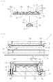
本発明に係る光素子の樹脂封止成形方法について、図面を参照して説明する。
図1(1)は、対象となる光素子を装着した基板の断面図および側面図を示す。
図1(2)は、本発明に係る樹脂封止成形方法を実施するために使用される樹脂封止成形用金型の断面図を示す。
図2乃至図5は、図1(2)に対応する金型要部の断面図であって、図1(1)に対応する基板を樹脂封止成形する実施方法を段階的に示す。
A resin sealing molding method for an optical element according to the present invention will be described with reference to the drawings.
FIG. 1A shows a cross-sectional view and a side view of a substrate on which a target optical element is mounted.
FIG. 1 (2) shows a cross-sectional view of a resin sealing molding die used for carrying out the resin sealing molding method according to the present invention.
2 to 5 are cross-sectional views of the main part of the mold corresponding to FIG. 1 (2), and show a step-by-step implementation method for resin sealing molding of the substrate corresponding to FIG. 1 (1).
例えば、図1(1)に示すように、対象となる基板15とは、円形状或いは多角形状である任意の形状で形成された基板15である。そして、基板15の一方の面に複数個のLEDチップ等の光素子16が装着された封止前基板24を使用する(図1(1)の左側部分)。封止前基板24は、透光性樹脂からなる樹脂材料17(図4参照)を加熱溶融化して生成した溶融樹脂18(図5(1)参照)によって少なくとも光素子16が封止される空間である封止成形部25を、一方の面に有する。また、封止前基板24は、一方の面における封止成形部25の外周囲において樹脂封止成形されない部分である基板外周部26と、基板15の他方の面の側に形成された非装着面27とを有する。樹脂封止後には、封止成形部25において溶融樹脂18が硬化して硬化樹脂19が形成されている。そして、樹脂封止後には、基板15の一方の面に硬化樹脂19が形成された光電子部品28(成形品)が完成する(図例の右側部分参照。)。この一括して形成された光電子部品28を、適宜な切断手段(図示なし)を使用して切断部位29(切断仮想線)に沿って切断分離する。これにより、個々の光電子部品30が完成する。
この封止成形部25において硬化した硬化樹脂19は、レンズ形状の略半球状を有する曲面部31と曲面部31の周囲における平面部32とによって構成される。図1(1)に示された基板15には、光素子16一個にそれぞれ対応する四個の曲面部31と、各曲面部31の間にある三個所の平面部32と、両側に形成された二個所の平面部32とが設けられている。
ところで、近年においては、次のような傾向が強まっている。それは、基板15の種類やボンディングの有無・方式のいかんを問わず、コストダウンのために基板15について大型化の要請が強くなっていることである。また、基板15の厚みが薄型化することである。また、光素子16自体が極薄化することである。また、一枚の基板15における光素子16の取れ数を大量に確保できるように、光素子16同士の間隔が狭小化することである。また、従来の短冊状の基板15に加えて、様々な大型化・薄型化した基板からなるマップ型(マトリクス型)の基板15、すなわち、マップ型(マトリクス型)基板15に装着された表面実装タイプの多数の光素子16を透光性樹脂17によって効率良く封止成形するという要請が強くなっていることである。
これらの傾向に応じて、例えば、光素子16一個に対して曲面部31一個が各別に形成される基板15ではなく、所定数の光素子16を一群として所要複数群に対して曲面部31が各別に且つ一括して形成される基板を使用してもよい。或いは、光電子部品28における平面部32が所定の厚みを有さないようにしてもよい。言い換えれば、全く平面部32が形成されずに曲面部31のみが形成される基板15であってもよい。更に、レンズ状の曲面部31からなる断面形状に代えて多角形の一部分からなる断面形状を有する封止成形部25であってもよい。
この透光性樹脂17からなる樹脂材料は、硬化した後に光素子16を保護する保護樹脂およびレンズとして機能する。樹脂材料としては、例えば、エポキシ樹脂またはシリコーン樹脂を使用する。また、樹脂材料として、顆粒状樹脂ではなく、液状樹脂、或いは、シート状樹脂を採用してもよい。
本発明によれば、従来のトランスファー成形用の金型を使用せずに、トランスファーレス成形用の樹脂封止成形用金型1を使用する。これにより、樹脂通路部分を全く設けないことによって、不要な樹脂部分を最小限に抑制させることができる。従って、環境問題に十分に配慮した樹脂封止成形装置が得られる。また、本発明によれば、様々な基板15、例えば、封止成形部25がレンズ形状の略半球状で構成された基板15に装着された光素子16に対して、以下に示す樹脂封止成形用金型1を使用して効率良く樹脂封止することができる。
For example, as shown in FIG. 1A, the
The cured
By the way, in recent years, the following tendencies have increased. That is, there is an increasing demand for an increase in the size of the
In accordance with these tendencies, for example, instead of the
The resin material made of the
According to the present invention, the resin-sealing molding die 1 for transferless molding is used without using the conventional transfer molding die. Thereby, an unnecessary resin part can be suppressed to the minimum by not providing the resin passage part at all. Therefore, a resin sealing molding apparatus with sufficient consideration for environmental problems can be obtained. In addition, according to the present invention, the following resin sealing is applied to the
この樹脂封止成形用金型1は、図1(2)に示すように、少なくとも、上型2と、上型2に相対向配置した下型3と、上型2と下型3との間に配置した中間型4との三型の構成を備える。また、下型3の側に設けたキャビティ面(下型キャビティ面5)と中間型4の下面(下型側金型面11)側との間に張設する離型フィルム7を使用する。図1(2)は、三型(上型2・下型3・中間型4)が型開きした状態を示す。固定された上型2は、上型面8を有する。上下動する下型3は、下型面9を有する。凸所33の天面は、下型キャビティ面5を構成する。上型2と下型3との間を上下動する中間型4は、上型側金型面10と下型側金型面11とを有する。
また、上型面8と上型側金型面10との間では、封止前基板24の供給と光電子部品28の取出とが行われる。下型側金型面11と下型面9(下型キャビティ面5)との間では、離型フィルム7の供給・送出が行われる。上型面8と下型キャビティ面5との間では、透光性樹脂17の供給が行われる。そして、離型フィルム7を介して下型3と中間型4とが上下方向に嵌装自在に型締め・型開きするように構成される。
なお、下型3・中間型4の型締め・型開き動作において使用される、油圧、水圧、空気圧、機械式等による適宜なプレス手段(図示なし)が設けられる。中間型4には、独立した別の適宜なプレス手段(図示なし)が設けられる。各プレス手段が、単動・連動して制御されることによって、樹脂封止成形用金型1を構成する上型2と下型3と中間型4とが図の上下方向に嵌装自在に型締め・型開きできるように構成される。
As shown in FIG. 1 (2), the resin sealing molding die 1 includes at least an
Further, between the
In addition, suitable press means (not shown) by hydraulic pressure, water pressure, air pressure, mechanical type, etc. used in the mold clamping and mold opening operations of the
樹脂封止成形用金型1のその他の構成要素としては、図1(2)に示すように、次のものがある。上型2には、基板装着固定手段34が設けられている。基板装着固定手段34は、上型2と中間型4との間に供給する基板15の封止成形部25の側を下方に向けて、上型面8の所定位置に基板15を装着固定する。また、上型面8には、外気遮断形成用のシール部材13が設けられている。シール部材13は、基板15を装着固定し、且つ、キャビティ全面に離型フィルム7を被覆して形成されたキャビティ空間部6内に透光性樹脂17(図例では顆粒状樹脂)を供給した状態で、少なくともキャビティ空間部6内を外気遮断状態にして外気遮断空間部14を形成する際に使用される。また、上型2には、吸引排出孔35が設けられている。吸引排出孔35は、上型2と中間型4との間にシール部材13を介在させることにより形成された外気遮断空間部14内の真空引きをする真空引き機構(図示なし)に連絡されている。
As other components of the resin sealing molding die 1, as shown in FIG. The
基板装着固定手段34は、例えば、従来の基板吸着固定方式に加えて、基板15を挟持する基板挟持固定方式を併用して、より一層確実に基板15を金型面(上型面8)に装着固定するように構成される。また、基板吸着固定方式としては、上型面8の所定位置に適宜な通気性部材(図示なし)を装設して非装着面27を吸引して吸着固定することができるように構成される。この場合には、光電子部品28(成形品)を樹脂封止した後に吸引と同様の経路を使用して、基板15の非装着面27を上型面8から離型するために圧送を併用できるようにも構成される。
また、基板挟持固定方式において使用される部材は、基板吸着固定方式において吸引する部分とシール部材13との間における基板外周部26に設けることが好ましい。また、基板15の基板外周部26が載置され、且つ、封止成形部25の全体に相当する部分に開口が設けられた適宜なチャック機構(図示なし)を使用してもよい。そして、例えば、大型化・薄型化した基板15であれば、基板外周部26全体をチャック機構で挟持固定する構成にしてもよい。また、従来から使用されている短冊状の基板15であれば、基板外周部26の所要複数箇所にチャック爪を備えた別のチャック機構(図示なし)を設けて、基板外周部26をチャック爪で挟持固定する構成でもよい。
従って、基板装着固定手段34において基板吸着固定方式と基板挟持固定方式とを組み合わせることによって、基板15(封止前基板24或いは光電子部品28)が、図示したとおり、確実に上型面8の所定位置に保持される。これにより、基板15自体が下方に向けて移動する基板15の反りを効率良く防止できて、基板15を効率良く装着固定することができる。
The substrate mounting / fixing means 34 uses, for example, a substrate clamping / fixing method for clamping the
Further, the member used in the substrate clamping and fixing method is preferably provided in the substrate outer
Therefore, by combining the substrate suction fixing method and the substrate clamping / fixing method in the substrate mounting / fixing means 34, the substrate 15 (the
吸引排出孔35は、基板装着固定手段34とシール部材13との間における上型面7側に開口して形成されている。また、吸引排出孔35は、外気遮断空間部14内から空気・ガス・水分等を強制的に吸引排出する真空引き機構に連絡する経路になるように所要複数個が設けられている。
真空引き成形を行う場合には、少なくともシール部材13、吸引排出孔35、真空引き機構を使用する。そして、中間型4が上動して上型側金型面10がシール部材13に当接して、上型2と中間型4とがシール部材13を介して接触することによって、外気遮断状態になった外気遮断空間部14を形成する。これと略同時に、外気遮断空間部14内を真空引きする真空引き機構に連絡する所要複数個の吸引排出孔35より、真空引きを行うことができる(図4(2)参照)。
従って、樹脂封止成形用金型1を使用して真空引き成形を行ったとしても、下型キャビティ面5を含む成形金型面に被覆されたキャビティ全面における離型フィルム7を上方に移動させることがないので、真空度を任意に調整できて、真空引き時間を削減し且つ十分にボイド(気泡)を除去して樹脂封止成形することができる。
The suction /
When vacuum drawing is performed, at least the
Accordingly, even if the vacuum molding is performed using the resin sealing molding die 1, the
中間型4には、図1(2)に示すように、金型貫通孔36が、図の上下方向に上型側金型面10から下型側金型面11まで中間型4を貫通して設けられる。また、この金型貫通孔36は、図3(1)に示すように、中間型4と下型3とを嵌装して型締めした状態において、キャビティ空間部6を含むことができるように構成される。
As shown in FIG. 1B, the intermediate mold 4 has a mold through
下型3には、挟持部材12やキャビティ部材20といった部材やその他の部材等が設けられている。それらの部材等を使用して、キャビティ空間部6を形成する方法、および、本発明の特徴部分である、特有の曲面形状を有する下型キャビティ面5を含む成形金型面、すなわちキャビティ全面の形状に沿って離型フィルム7を被覆する方法を、以下に説明する。
The
まず、図1(2)に示す三型(上型2・下型3・中間型4)の型開き状態から、中間型4が下動する。ここで、略中央部分においてキャビティ全面を含む貫通孔37を備えた離型フィルム用の挟持部材12が、中間型4に相対向して設けられている。そして、下型側金型面11側の金型貫通孔36の周縁部と離型フィルム用の挟持部材12の天面とによって離型フィルム7を挟持する。この挟持部材12に付設されるものとして、図の上下方向に沿って伸びる所要複数個の取付棒38と、挟持部材12・取付棒38を上下動に弾性的に摺動させるスプリング等からなる適宜な弾性部材39とが少なくとも設けられている。つまり、図1(2)に示す型開き状態では、下型3に設けた挟持部材12の天面が上方に突出した状態で、且つ、弾性部材39が復元した状態で待機する。そして、中間型4と下型3とを型締めすると、挟持部材12・取付棒38が一体となって下動すると同時に、弾性部材39が縮んだ状態になる。
First, the intermediate mold 4 moves down from the mold open state of the three molds (
次に、中間型4と下型3の挟持部材12とで離型フィルム7を挟持した状態で、更に中間型4と挟持部材12とを一体で下動させる。これにより、図2(1)に示すように、挟持部材12に挟持されない部分、すなわち貫通孔37に重なる部分の離型フィルム7が、キャビティ部材20の天面の基板当接部位40に当接する。このキャビティ部材20は、下型キャビティ面5を備えた凸所33の外周囲に嵌入される。また、キャビティ部材20には、凸所33を収容するように凸所33に重なる部分に開口が設けられている。
このキャビティ部材20の断面形状は、図例のとおり、L字形状をしている。キャビティ部材20におけるL字形状の垂直部分には、次の構成要素が設けられている。それらの構成要素は、主に、離型フィルム7を介して基板外周部26に当接する基板当接部位40である。また、下型キャビティ面5の外周囲に配置され、下型キャビティ面5と併せてキャビティの底面を形成するキャビティ外周面22である。また、基板当接部位40の面とキャビティ外周面22との間に設けられたキャビティ側面23である。そして、キャビティ部材20におけるL字形状の水平部分には、次の構成要素が設けられている。それらの構成要素は、挟持部材12が載置される上面と、キャビティ部材20が下動した場合に下型面9に当接する下面とである。また、キャビティ部材20を上下方向に弾性的に摺動させるスプリング等からなる適宜な弾性部材41である。弾性部材41は、下型面9よりも凹んだ部分に嵌装される。
つまり、図1(2)に示す型開き状態では、キャビティ部材20の基板当接部位40の面およびキャビティ面21(キャビティ外周面22・キャビティ側面23)が、下型キャビティ面5よりも上方に突出し且つ挟持部材12の天面よりも低い位置で待機する。また、弾性部材41が復元した状態で待機する。そして、中間型4と下型3とが嵌装して型締めする図5(2)に示す状態になると、キャビティ部材20における水平部分の上面と挟持部材12の底面とが、および、キャビティ部材20における水平部分の下面と下型面9とが当接して、弾性部材41が最も縮んだ状態になる。
ここで、キャビティ部材20のキャビティ面21(キャビティ外周面22とキャビティ側面23)と、凸所33の天面における下型キャビティ面5とが、キャビティ全面を構成している。
Next, in a state where the
The cross-sectional shape of the
That is, in the mold open state shown in FIG. 1 (2), the surface of the
Here, the cavity surface 21 (cavity outer
次に、中間型4と下型3の挟持部材12とで離型フィルム7を挟持した状態で、更に中間型4と挟持部材12とを一体で下動させる。これによって、図2(2)に示す状態を経て、図3(1)に示すように、中間型4と下型3とが嵌装された状態で型締めして、キャビティ空間部6が形成される。そして、挟持部材12の底面とキャビティ部材20の水平部分の上面とが当接する。このとき、キャビティ部材20の水平部分の下面と下型面9とは離間した状態であって、キャビティ部材20の弾性部材41も復元した状態である。
また、図3(1)に示すように、キャビティ全面に離型フィルム7を被覆し且つ下型キャビティ面5に離型フィルム7を確実にフィットさせる。これを実現するために、図2(1)に示すように、挟持部材12の天面と中間型4とが離型フィルム7を挟持した状態で中間型4を下動させる。このことにより、基板当接部位40の内側において挟持されていない状態にあって、且つ、樹脂封止成形用金型1により加熱されていることによって柔軟になっている離型フィルム7が、伸張する。これらによって、伸張した離型フィルム7がキャビティ全面の形状に沿って被覆する。したがって、光電子部品28が有するレンズ形状の曲面部31(図1(1)参照)に対応して少なくとも下型キャビティ面5に形成された特有の曲面形状にも、離型フィルム7を確実にフィットさせることができる。
従って、キャビティ全面の形状に沿って、離型フィルム7を効率良く被覆し且つ確実に下型キャビティ面5にフィットさせているので、高密着性を有する樹脂材料(透光性樹脂17)を使用した場合においても、硬化樹脂19が型面に付着することなく効率良く光電子部品28を離型することができる。
Next, in a state where the
Further, as shown in FIG. 3 (1), the
Accordingly, the
この離型フィルム7を下型キャビティ面5に確実にフィットさせるために、下型キャビティ面5が形成された凸所33に、および/または、キャビティ部材20のキャビティ面21を形成する部位に、離型フィルム7を強制的に吸引する適宜なフィルム吸着固定手段(図示なし)を設ける構成を採用することが好ましい。この場合においては、吸着固定する対象が基板15でなく離型フィルム7ではあるが、前述した基板装着固定手段34における基板吸着固定方式とほぼ同様の構成を採用してもよい。
このフィルム装着固定手段を使用して、少なくとも下型面9の所定位置(下型キャビティ面5)に離型フィルム7を強制的に吸引して吸着固定することができる。そして、図5(3)に示す状態、すなわち光電子部品28(成形品)を樹脂封止した後に中間型4と下型3とを型開きして下型3のみを下動する状態において、吸引排出作用と同様の経路を使用して、封止成形部25において硬化した部分(硬化樹脂19)を離型フィルム7を介して圧送する、下型面9から光電子部品28(成形品)を離型するための圧送機構も併用することができる。これによれば、基板15の大型化・薄型化が進んだとしても、従来のエジェクタピン等の突き出し部材を使用せずに、光電子部品28を圧送して離型することができる。したがって、硬化樹脂19をより一層損傷しないようにして、光電子部品28を効率良く離型することができる。また、硬化樹脂19は高温時の硬度が低いことから、樹脂封止成形用金型1から離型する際に型面に付着しやすくなる。この場合においても、下型キャビティ面5にフィットしたフィルム皺のない離型フィルム7によって、硬化樹脂19の部分を効率良く離型することができる。
また、下型キャビティ面5に離型フィルム7をフィットさせるために、好ましくは、キャビティ全面に被覆される離型フィルム7にエアブローする、特に、特有の曲面形状に対してエアブローするエアブロー機構42を設けてもよい(図2(2)参照。)。このエアブロー機構42によれば、より一層キャビティ全面(下型キャビティ面5・キャビティ面21)の形状に沿って、伸張した離型フィルム7を被覆させることができる。
また、離型フィルム7を確実にフィットさせるために、前述した方法を適宜に組み合わせることもできる。これらによって、基板15に装着された様々な光素子16に対応する様々な特有の曲面形状を含む任意の形状で形成されたキャビティを有する下型キャビティ面5に、離型フィルム7を効率良く被覆でき且つ確実にフィットさせることができる。
In order to securely fit the
By using this film mounting and fixing means, the
Further, in order to fit the
Moreover, in order to make the
ここで、図2(1)に示す状態から図3(1)に示すキャビティ空間部6を形成するまでの過程において、キャビティ全面の形状に沿って確実に被覆する離型フィルム7は、樹脂封止成形用金型1全体により加熱されていることによって柔軟になって伸張することに加えて、耐熱性、耐久性に優れている。そして、様々な形状、例えば、特有の曲面形状、その他の任意の形状を有するキャビティが設けられている下型キャビティ面5においても、離型フィルム7が上方に移動すること、および、キャビティに被覆された離型フィルム7にフィルム皺が発生することが防止される。特に、光電子部品28が有するレンズ形状の曲面部31(図1(1)参照)に対応する型面において、離型フィルム7の凹凸が効率良く防止される。これらによって、樹脂封止後の光電子部品28のレンズ面および個々の光電子部品30のレンズ面を鏡面状態に確保することができる。
Here, in the process from the state shown in FIG. 2 (1) to the formation of the
ここで、本発明に係る光素子16の樹脂封止成形方法について、図1乃至図5を参照して、以下に段階的に説明する。
Here, the resin sealing molding method of the
まず、図1(2)に示すように、上型2と下型3と中間型4(樹脂封止成形用金型1)が型開きした状態において、下型キャビティ面5と中間型4の下面(下型側金型面11)との間に離型フィルム7を張設する。
First, as shown in FIG. 1 (2), when the
次に、図2(1)に示すように、離型フィルム7が中間型4の下型側金型面11に当接した状態で、下型側金型面11と挟持部材12の天面とによって離型フィルム7を挟持する。そして、この状態で、中間型4と挟持部材12とを一体となって下動させる。これにより、図2(2)の状態を経て、挟持部材12の底面とキャビティ部材20の水平部分の上面とが当接する(図3(1)参照)。ここで、図2(2)に示されているように、エアブロー機構42を使用して、下型キャビティ面5に向かって離型フィルム7をエアブローする。これにより、中間型4の金型貫通孔36(挟持部材12の貫通孔37に対応)において挟持されていない伸張した状態の離型フィルム7を、少なくとも下型キャビティ面5とキャビティ面21(キャビティ外周面22・キャビティ側面23)とを含むキャビティ全面の形状に沿って確実に被覆させることができる。ここまでの工程により、キャビティ空間部6を形成する。
Next, as shown in FIG. 2 (1), with the
次に、図3(2)に示すように、一体型の搬送手段43を、樹脂封止成形用金型1の内部(上型2と中間型4及び下型3との間)に進入させる。この搬送手段43には、上型面8に対向する側には封止成形部25の部分を下方に向けた封止前基板24が固定され、下型キャビティ面5に対向する側には所要量の透光性樹脂17が収容されている。この一体型の搬送手段43に代えて、基板15と透光性樹脂17とを夫々の搬送手段で各別に供給してもよく、前述したエアブロー機構42を一体型の搬送手段43に備えてもよい。
Next, as shown in FIG. 3 (2), the integrated conveying
次に、図4(1)に示すように、封止前基板24の非装着面27を上型面8の所定位置に基板装着固定手段34にて確実に装着固定する。また、キャビティ空間部6に所要量の透光性樹脂17を供給する。そして、キャビティ空間部6に供給された所要量の透光性樹脂17を、好ましくは、透光性樹脂17が加熱溶融化するのに必要な所定の温度の近傍まで、樹脂封止成形用金型1全体を使用して加熱する。
ここまでの図1(2)乃至図4(1)に示す各工程において、封止前基板24の上型面8への装着固定、キャビティ空間部6の形成、樹脂封止成形用金型1全体の予備加熱、或いは、キャビティ空間部6への透光性樹脂17の供給等の実施順序については、後述する図4(2)に示す真空引き工程までに実施できれば、適宜に変更することができる。
Next, as shown in FIG. 4 (1), the
In each of the steps shown in FIGS. 1 (2) to 4 (1) up to this point, mounting and fixing to the
次に、図4(2)に示すように、キャビティ空間部6内に透光性樹脂17を供給した状態で、上型2と中間型4及び下型3とを嵌装させることによって中間型締め状態を実現する。この状態において、上型面8に設けられたシール部材13に上型側金型面10が当接することによってシール部材13がつぶれた状態となる。これによって、少なくとも、キャビティ空間部6を外気遮断状態にして外気遮断空間部14が形成される。これと略同時に、真空引き機構に連絡する吸引排出孔35を使用して、外気遮断空間部14における空気を強制的に吸引して排出する(図4(2)の破線矢印部分)。なお、キャビティ空間部6における透光性樹脂17は、図4(2)に示す状態で溶融化していなくても、図5(1)に示す状態までに溶融化していれば、強制的に吸引するタイミングを適宜に変更して実施できる。また、樹脂封止成形用金型1の真空引き工程を、中間型締め状態(図4(2)参照。)で実施するようにしている。これに限らず、中間型締め状態と完全型締め状態(図5(2)参照。)とにおいて真空引き工程を断続的に実施してもよい。また、樹脂封止成形用金型1の型締め動作を停止させることなく、前述した中間型締め状態の位置から完全型締め状態の位置に至るまでの間、型締めの速度(樹脂封止成形用金型1の型締め速度)を遅くしながら連続的に真空引き工程を行うように適宜に変更して実施できる。
Next, as shown in FIG. 4 (2), the
次に、図5(1)に示すように、上型2と中間型4及び下型3とを更に嵌装させて中間型4と下型3とを一体として上動することにより、キャビティ空間部6の基板当接部位40の面が、封止前基板24の基板外周部26に離型フィルム7を介して当接する。これにより、キャビティ空間部6の溶融樹脂18に光素子16が浸漬される。このとき、キャビティ空間部6に被覆した離型フィルム7は、溶融樹脂18によって、キャビティ部材20のキャビティ面21を構成するキャビティ外周面22とキャビティ側面23とにフィットする。そして、離型フィルム7は、フィルム皺を発生することなく、より一層、キャビティ面21の形状に沿って効率良く被覆され且つ確実にフィットする。また、離型フィルム7は、下型キャビティ面5においても、溶融樹脂18によって、より一層フィルム皺を発生することなく、凹凸を形成することなく、下型キャビティ面5の特有の曲面形状に沿って確実にフィットする。
また、キャビティ空間部6における突出した基板当接部位40の部分が、離型フィルム7を介して基板外周部26を確実に当接する。従って、図5(2)に示す完全型締め状態において、溶融樹脂18が封止成形部25(図1(1)参照)に完全に充填された状態になったとしても、基板外周部26上に溶融樹脂18が漏出することを効率良く防止することができる。
Next, as shown in FIG. 5 (1), the
Further, the protruding portion of the
次に、図5(2)に示すように、図5(1)に示す封止前基板24が基板当接部位40に当接した状態から、中間型4と下型3とが更に嵌装して下型3(凸所33の部分)のみを上動させる。これにより、下型キャビティ面5がキャビティ外周面22と略同一平面上となり、封止成形部25(図1(1)参照)に完全に溶融樹脂18が充填される。
この図5(2)に示す状態に至るまで、挟持部材12とキャビティ部材20とが当接状態のままで、一体となって下動する。これによって、キャビティ部材20の水平部分の下面と下型面9とが当接すると共に、下型2に設けた各弾性部材39・41が最も縮んだ状態となる。図5(2)に示された状態が、樹脂封止成形用金型1(上型2・下型3・中間型4)の完全型締め状態となる。
なお、樹脂封止成形用金型1の完全型締め状態については、キャビティ空間部6を形成する下型キャビティ面5における曲面以外の平面とキャビティ外周面22とを略同一平面上にして実施するように説明している。これに限らず、様々な基板15に対応して、キャビティ空間部6における樹脂量を調整することができるようにしてもよい。例えば、キャビティ外周面22よりも下型キャビティ面5を図の上下方向に高い位置、或いは、低い位置に適宜設定することで、封止成形部25の厚み、この場合、封止成形部25の平面部32の厚みを任意に変更する構成にしてもよい。
例えば、平面部32の厚みを完全になくすのであれば、キャビティ空間部6に透光性樹脂17を供給する際には、キャビティ空間部6の全体に透光性樹脂17を供給するのではなく、キャビティ空間部6において曲面形状を有する部分のみに、所要量の透光性樹脂17を供給することができる。
そして、樹脂成形圧力については、従来のトランスファー成形での樹脂成形圧力と同じか、或いは、低い樹脂成形圧力で、適宜に変更して実施できる。この場合、下型3の凸所33における天面である下型キャビティ面5に被覆された離型フィルム7を介して型締め圧力をモニタリングできるように圧力センサー等の測定機器(図示なし)を凸所33に埋設する構成にしてもよい。
また、真空引きを解除するタイミングは、中間型締め状態(図4(2)参照。)から完全型締め状態(図5(2)参照。)になるまでの間において、適宜に変更して実施することができる。この場合において、好ましくは、図5(2)に示す完全型締め状態まで真空引きを継続して、樹脂封止完了後に解除する。
従って、樹脂封止成形用金型1を弾性的に支受して水平状態を保持するので、樹脂封止成形用金型1を各プレス手段のみで上下動させる際に、上型面8、下型面9、上型側金型面10、及び下型側金型面11が突き当たる際の衝撃を和らげることができる。また、従来のトランスファーレス成形の三型構成の金型において、特有の曲面形状で形成されたキャビティの形状に沿って離型フィルム7がうまく被覆されないこと、キャビティ全面に離型フィルムが被覆されていないこと等による樹脂成形上の問題を効率良く解決することができる。
Next, as shown in FIG. 5 (2), the intermediate mold 4 and the
Until the state shown in FIG. 5 (2) is reached, the clamping
Note that the completely sealed state of the resin sealing molding die 1 is carried out with the plane other than the curved surface of the lower
For example, if the thickness of the
And about resin molding pressure, it can carry out by changing suitably at the same resin molding pressure in the conventional transfer molding, or low resin molding pressure. In this case, a measuring device (not shown) such as a pressure sensor is used so that the clamping pressure can be monitored through the
Further, the timing for releasing the vacuuming is appropriately changed between the intermediate clamping state (see FIG. 4 (2)) and the complete clamping state (see FIG. 5 (2)). can do. In this case, preferably, vacuuming is continued until the complete mold clamping state shown in FIG. 5 (2), and is released after the resin sealing is completed.
Accordingly, since the resin sealing molding die 1 is elastically supported and kept in a horizontal state, when the resin sealing molding die 1 is moved up and down only by each pressing means, the
次に、図示していないが、樹脂封止成形用金型1を図5(2)に示す完全型締め状態に保持しながら、封止成形部25における溶融樹脂18を硬化するための所要時間を経過させる。これにより、溶融樹脂18を硬化させて硬化樹脂19を形成して、最終的に、光電子部品28(成形品)を完成させる(図1(1)参照。)。
Next, although not shown, the time required for curing the
次に、樹脂封止成形された光電子部品28(成形品)を樹脂封止成形用金型1および離型フィルム7から離型するために、図5(2)に示す完全型締め状態から図5(1)の状態へ移行する。まず、図5(3)に示すように、中間型4と下型3とを型開きして下型3(凸所33の部分)のみを下動させる。これにより、下型キャビティ面5が下動して下型キャビティ面5の上面がキャビティ外周面22よりも低い位置に戻る。すると、硬化樹脂19の部分に被覆された離型フィルム7と下型キャビティ面5との間に隙間ができて、離型フィルムを7介して下型キャビティ面5から光電子部品28(成形品)を離型することができる。
Next, in order to release the resin-encapsulated optoelectronic component 28 (molded product) from the resin-encapsulating
次に、図示していないが、光電子部品28(成形品)が下型面19の所定位置(下型キャビティ面5)から離型した状態で、上型2と中間型4および下型3とを、更に型開きする。次に、上型面8の所定位置に装着固定された光電子部品28(成形品)を樹脂封止成形用金型1の外へ取り出すために、図3(2)に示された状態とほぼ同様にして、一体型の搬送手段43を上型2と中間型4及び下型3との間に進入させる。そして、上型面8の所定位置から光電子部品28(成形品)を取り出す。このとき、一体型の搬送手段43が樹脂封止成形用金型1の外に退出する際に、適宜なクリーニング機構(図示なし)にて使用済の離型フィルム7をクリーニングしてもよい。これにより、樹脂封止成形用金型1の内外をクリーンな状態に維持させて、光電子部品28(成形品)の品質レベルをより一層向上させることができる。なお、封止前基板24および透光性樹脂17の搬送と光電子部品28(成形品)の搬送とを、同一の搬送手段43、或いは、各別の搬送手段43であるメカチャック搬送機構やロボットアーム搬送機構等を使用して実施する。
Next, although not shown in the figure, the optoelectronic component 28 (molded product) is released from a predetermined position (the lower mold cavity surface 5) of the
以上のような一連の樹脂封止工程を経て、封止前基板24を光電子部品28(成形品)に樹脂封止成形することができる。当然のことながら、この一連の樹脂封止工程については、連続的、或いは、断続的に、稼動・停止させるように適宜に変更して実施できる。
Through the series of resin sealing steps as described above, the
以上説明したように、本発明に係る光素子16の樹脂封止成形方法によれば、様々な基板15に装着された光素子16を樹脂封止成形する際に、樹脂封止成形用金型1(上型2・下型3・中間型4)と透光性樹脂17(高密着性を有する樹脂材料も含む)からなる硬化樹脂19との離型性が格段に向上する。また、光電子部品28(成形品)と樹脂封止成形用金型1との離型性が格段に向上する。そして、これらの離型フィルム成形の長所、および、様々な透光性樹脂17を加熱溶融化する際に発生するボイド(気泡)を防止する真空引き成形の長所を生かすことができる。また、樹脂封止成形する際に、離型フィルム7を、キャビティ全面の形状に沿って効率良く被覆させることができ、且つ、下型キャビティ面5に確実にフィットさせることができる。これらによって、様々な基板15・透光性樹脂17を使用して、品質レベルを向上させて効率良く樹脂封止成形することができる。
As described above, according to the resin sealing molding method of the
なお、本実施形態においては、固定された上型2と上下方向に嵌装自在な中間型4と下型3とから成る樹脂封止成形用金型1について説明した。これに限らず、樹脂封止成形用金型1において可動させる部分を任意に変更させて実施することもできる。また、上型2ではシール部材13、基板装着固定手段34、吸引排出孔35を含む構成とし、中間型4では金型貫通孔36を含む構成とし、下型3では挟持部材12(取付棒38・弾性部材39を含む)、キャビティ部材20(弾性部材41を含む)を含む構成とした。そして、上型面8の所定位置に基板15を装着固定させ、且つ、キャビティ空間部6におけるキャビティ全面に離型フィルム7を被覆するようにした。これに限らず、基板15や離型フィルム7の装着固定を満足させるのであれば、適宜に各手段・各機構・各部材の形状・配置・数量等の構成要件を変更させて対応することも可能である。
また、樹脂材料として、顆粒状樹脂である透光性樹脂17を使用して封止成形する構成について説明した。これに代えて、顆粒状樹脂ではなく液状樹脂・粉末状樹脂、或いは、粉末よりも粒径が大きく顆粒よりも粒径の小さい微粒状樹脂を採用して実施することも適宜可能である。
また、前述の樹脂封止成形を、ワイヤで基板15と光素子16をワイヤボンディングするワイヤボンディング基板、ワイヤの無いバンプを介して光素子16と接続するフリップチップ基板、或いは、ウェーハ基板等においても適用することが可能である。
In the present embodiment, the resin sealing molding die 1 including the fixed
Moreover, the structure which seal-molds using the
In addition, the above-described resin sealing molding may be applied to a wire bonding substrate for wire-bonding the
1 樹脂封止成形用金型
2 上型
3 下型
4 中間型
5 下型キャビティ面
6 キャビティ空間部
7 離型フィルム
8 上型面
9 下型面
10 上型側金型面
11 下型側金型面
12 挟持部材
13 シール部材
14 外気遮断空間部
15 基板
16 光素子
17 透光性樹脂(樹脂材料)
18 溶融樹脂
19 硬化樹脂
20 キャビティ部材
21 キャビティ面
22 キャビティ外周面
23 キャビティ側面
24 封止前基板
25 封止成形部
26 基板外周部
27 非装着面
28 光電子部品(成形品)
29 切断部位
30 個々の光電子部品
31 曲面部
32 平面部
33 凸所
34 基板装着固定手段
35 吸引排出孔
36 金型貫通孔
37 貫通孔
38 取付棒
39・41 弾性部材
40 基板当接部位
42 エアブロー機構
43 搬送手段
DESCRIPTION OF
DESCRIPTION OF
DESCRIPTION OF
Claims (18)
前記上型と前記中間型との間にシール部材を介在させることによって前記キャビティ空間部を含む外気遮断空間部を形成する工程と、
前記外気遮断空間部を真空引きする工程とを備えると共に、
前記キャビティ空間部を形成する工程では前記下型キャビティ面に対して前記離型フィルムをフィットさせ、前記離型フィルムをフィットさせる際に、少なくとも前記下型キャビティ面に被覆させる前記離型フィルムにエアブローし、
前記位置合わせする工程では前記複数の光素子の各々が、または、前記複数の光素子に含まれる複数の光素子からなる一群が複数集まって構成される複数群のうち前記一群の各々が、平面視した場合に前記複数の凹部の各々に重なるようにして前記基板を位置合わせし、
前記浸漬する工程では前記下型キャビティ面を含むキャビティ全面に前記離型フィルムが被覆されており、かつ、前記中間型と前記下型との間において前記離型フィルムを挟持していることを特徴とする光素子の樹脂封止成形方法。 Three molds for transferless molding of an upper mold and a lower mold disposed opposite to the upper mold and provided with a cavity having a plurality of recesses, and an intermediate mold disposed between the upper mold and the lower mold A step of preparing a mold for resin sealing molding and a release film stretched above the cavity, and a lower mold cavity surface including mold surfaces in the plurality of recesses is covered with the release film Forming a cavity space thereby, aligning a substrate on which a plurality of optical elements are mounted at a predetermined position so that the plurality of optical elements face the lower mold cavity surface, and fluidity; The step of filling the cavity space with a resin material having translucency, and clamping the plurality of optical elements by clamping the mold for resin sealing molding A step of immersing in a fat material; a step of curing the resin material to form a cured resin; a step of opening the mold for resin sealing molding; the substrate; the plurality of optical elements; and the cured resin. A step of taking out a molded product including
Forming an outside air blocking space including the cavity space by interposing a seal member between the upper mold and the intermediate mold;
And evacuating the outside air blocking space part,
In the step of forming the cavity space, the release film is fitted to the lower mold cavity surface, and at the time of fitting the release film, at least air blow is applied to the release film that covers the lower mold cavity surface. And
In the aligning step, each of the plurality of optical elements or each of the one group out of a plurality of groups formed by a plurality of groups of optical elements included in the plurality of optical elements is a plane Aligning the substrate so as to overlap each of the plurality of recesses when viewed,
In the dipping step, the release film is coated on the entire cavity including the lower mold cavity surface, and the release film is sandwiched between the intermediate mold and the lower mold. A resin sealing molding method of an optical element.
前記上型と前記中間型との間にシール部材を介在させることによって前記キャビティ空間部を含む外気遮断空間部を形成する工程と、
前記外気遮断空間部を真空引きする工程とを備え、
前記キャビティ空間部を形成する工程の前に前記離型フィルムを挟持する工程を備えると共に、
前記キャビティ空間部を形成する工程では、挟持された前記離型フィルムを前記下型キャビティ面に向かって吸引することまたはエアブローすることの少なくとも一方を実施することによって前記下型キャビティ面に前記離型フィルムをフィットさせ、
前記位置合わせする工程では前記複数の光素子の各々が、または、前記複数の光素子に含まれる複数の光素子からなる一群が複数集まって構成される複数群のうち前記一群の各々が、平面視した場合に前記複数の凹部の各々に重なるようにして前記基板を位置合わせし、
前記浸漬する工程では前記下型キャビティ面を含むキャビティ全面に前記離型フィルムが被覆されており、かつ、前記中間型と前記下型との間において前記離型フィルムを挟持していることを特徴とする光素子の樹脂封止成形方法。 Three molds for transferless molding of an upper mold and a lower mold disposed opposite to the upper mold and provided with a cavity having a plurality of recesses, and an intermediate mold disposed between the upper mold and the lower mold A step of preparing a mold for resin sealing molding and a release film stretched above the cavity, and a lower mold cavity surface including mold surfaces in the plurality of recesses is covered with the release film Forming a cavity space thereby, aligning a substrate on which a plurality of optical elements are mounted at a predetermined position so that the plurality of optical elements face the lower mold cavity surface, and fluidity; The step of filling the cavity space with a resin material having translucency, and clamping the plurality of optical elements by clamping the mold for resin sealing molding A step of immersing in a fat material; a step of curing the resin material to form a cured resin; a step of opening the mold for resin sealing molding; the substrate; the plurality of optical elements; and the cured resin. A step of taking out a molded product including
Forming an outside air blocking space including the cavity space by interposing a seal member between the upper mold and the intermediate mold;
Vacuuming the outside air blocking space, and
Including a step of sandwiching the release film before the step of forming the cavity space,
In the step of forming the cavity space, the mold release is performed on the lower mold cavity surface by performing at least one of sucking or air blowing the sandwiched release film toward the lower mold cavity surface. Fit the film,
In the aligning step, each of the plurality of optical elements or each of the one group out of a plurality of groups formed by a plurality of groups of optical elements included in the plurality of optical elements is a plane Aligning the substrate so as to overlap each of the plurality of recesses when viewed,
In the dipping step, the release film is coated on the entire cavity including the lower mold cavity surface, and the release film is sandwiched between the intermediate mold and the lower mold. A resin sealing molding method of an optical element.
前記上型と前記中間型との間にシール部材を介在させることによって前記キャビティ空間部を含む外気遮断空間部を形成する工程と、
前記外気遮断空間部を真空引きする工程とを備えると共に、
前記キャビティ空間部を形成する工程では、前記下型キャビティ面に向かって前記離型フィルムをエアブローすることによって前記下型キャビティ面を含むキャビティ全面に沿って前記下型キャビティ面に前記離型フィルムをフィットさせ、
前記浸漬する工程では前記下型キャビティ面を含むキャビティ全面に前記離型フィルムが被覆されており、かつ、前記中間型と前記下型との間において前記離型フィルムを挟持していることを特徴とする光素子の樹脂封止成形方法。 Three molds for transferless molding of an upper mold and a lower mold disposed opposite to the upper mold and provided with a cavity having a plurality of recesses, and an intermediate mold disposed between the upper mold and the lower mold A mold for resin sealing molding, and a step of preparing a release film stretched between a lower mold cavity surface including a mold surface in the plurality of recesses and a lower surface of the intermediate mold, and the release film A step of forming a cavity space by covering at least the lower mold cavity surface using a resin, a step of filling the cavity space with a resin material having fluidity and translucency, and Clamping the upper mold and the intermediate mold, and immersing the plurality of optical elements in the resin material by accommodating the plurality of optical elements mounted on a substrate in the cavity space; Forming the cured resin by curing the resin material, and sealing the plurality of optical elements with the cured resin, thereby forming the molded article including the substrate, the plurality of optical elements, and the cured resin. A resin sealing molding method of an optical element for forming
Forming an outside air blocking space including the cavity space by interposing a seal member between the upper mold and the intermediate mold;
And evacuating the outside air blocking space part,
In the step of forming the cavity space, the release film is blown onto the lower mold cavity surface along the entire cavity including the lower mold cavity surface by air blowing the release film toward the lower mold cavity surface. Fit,
In the dipping step, the release film is coated on the entire cavity including the lower mold cavity surface, and the release film is sandwiched between the intermediate mold and the lower mold. A resin sealing molding method of an optical element.
前記上型と前記中間型との間にシール部材を介在させることによって前記キャビティ空間部を含む外気遮断空間部を形成する工程と、
前記外気遮断空間部を真空引きする工程とを備え、
前記キャビティ空間部を形成する工程の前に、前記下型キャビティ面と前記中間型の下面との間において前記離型フィルムを挟持する工程を備えると共に、
前記キャビティ空間部を形成する工程では、挟持された前記離型フィルムを前記下型キャビティ面に向かって吸引することまたはエアブローすることの少なくとも一方を実施することによって前記下型キャビティ面を含むキャビティ全面に沿って前記下型キャビティ面に前記離型フィルムをフィットさせ、
前記浸漬する工程では前記下型キャビティ面を含むキャビティ全面に前記離型フィルムが被覆されており、かつ、前記中間型と前記下型との間において前記離型フィルムを挟持していることを特徴とする光素子の樹脂封止成形方法。 Three molds for transferless molding of an upper mold and a lower mold disposed opposite to the upper mold and provided with a cavity having a plurality of recesses, and an intermediate mold disposed between the upper mold and the lower mold A mold for resin sealing molding, and a step of preparing a release film stretched between a lower mold cavity surface including a mold surface in the plurality of recesses and a lower surface of the intermediate mold, and the release film A step of forming a cavity space by covering at least the lower mold cavity surface using a resin, a step of filling the cavity space with a resin material having fluidity and translucency, and Clamping the upper mold and the intermediate mold, and immersing the plurality of optical elements in the resin material by accommodating the plurality of optical elements mounted on a substrate in the cavity space; Forming the cured resin by curing the resin material, and sealing the plurality of optical elements with the cured resin, thereby forming the molded article including the substrate, the plurality of optical elements, and the cured resin. A resin sealing molding method of an optical element for forming
Forming an outside air blocking space including the cavity space by interposing a seal member between the upper mold and the intermediate mold;
Vacuuming the outside air blocking space, and
Before the step of forming the cavity space, comprising the step of sandwiching the release film between the lower mold cavity surface and the lower surface of the intermediate mold,
In the step of forming the cavity space portion, the entire cavity including the lower mold cavity surface is performed by performing at least one of sucking or air blowing the sandwiched release film toward the lower mold cavity surface. Fit the release film to the lower cavity surface along
In the dipping step, the release film is coated on the entire cavity including the lower mold cavity surface, and the release film is sandwiched between the intermediate mold and the lower mold. A resin sealing molding method of an optical element.
前記樹脂封止成形装置はトランスファーレス成形用であり、
前記上型と前記中間型との間に設けられたシール部材と、
前記キャビティ空間部を含む外気遮断空間部を減圧する真空引き機構と、
前記離型フィルムを前記下型キャビティ面に向かってエアブローするエアブロー機構とを備えると共に、
前記離型フィルムが前記下型キャビティ面に向かってエアブローされることによって前記下型キャビティ面に前記離型フィルムがフィットし、
前記上型と前記中間型との間にシール部材が介在することによって前記外気遮断空間部が形成され、
前記上型と前記下型と前記中間型とが型締めした状態において、前記複数の光素子が前記キャビティ空間部に収容され、且つ、前記複数の光素子の各々が、または、前記複数の光素子に含まれる複数の光素子からなる一群が複数集まって構成される複数群のうち前記一群の各々が、平面視した場合に前記複数の凹部の各々に重なっており、
前記下型キャビティ面を含むキャビティ全面に前記離型フィルムが被覆されており前記キャビティ空間部に存在する前記樹脂材料に前記複数の光素子が浸漬された状態で、かつ、前記中間型と前記下型との間において前記離型フィルムが挟持されている状態で、前記樹脂材料が硬化することを特徴とする光素子の樹脂封止成形装置。 An upper mold, a lower mold provided with a cavity having a plurality of recesses disposed opposite to the upper mold, an intermediate mold disposed between the upper mold and the lower mold, and mold surfaces in the plurality of recesses A tensioning mechanism for tensioning a release film between a lower mold cavity surface including the intermediate mold and a covering mechanism for forming a cavity space by covering the lower mold cavity surface with the release film; A cured resin is formed by curing a resin material having fluidity and translucency that exists in the cavity space in a state where the upper mold, the lower mold, and the intermediate mold are clamped, A plurality of optical elements mounted on the substrate fixed to the upper mold are collectively encapsulated with the cured resin to form a molded product including the substrate, the plurality of optical elements, and the cured resin. Used when A resin sealing and molding apparatus that the optical device,
The resin sealing molding apparatus is for transferless molding,
A seal member provided between the upper mold and the intermediate mold;
A vacuum drawing mechanism for depressurizing the outside air blocking space including the cavity space;
An air blow mechanism for air blowing the release film toward the lower mold cavity surface;
The release film fits to the lower mold cavity surface by air blowing toward the lower mold cavity surface,
The outside air blocking space is formed by a seal member interposed between the upper mold and the intermediate mold,
In a state in which the upper mold, the lower mold, and the intermediate mold are clamped, the plurality of optical elements are accommodated in the cavity space, and each of the plurality of optical elements or the plurality of lights Each of the one group out of a plurality of groups configured by a plurality of groups of a plurality of optical elements included in the element overlaps each of the plurality of recesses when viewed in plan,
The release film is coated on the entire cavity surface including the lower mold cavity surface, and the plurality of optical elements are immersed in the resin material existing in the cavity space, and the intermediate mold and the lower mold A resin sealing molding apparatus for an optical element, wherein the resin material is cured in a state where the release film is sandwiched between molds.
前記樹脂封止成形装置はトランスファーレス成形用であり、
前記中間型との間において前記離型フィルムを挟持する挟持機構と、
前記上型と前記中間型との間に設けられたシール部材と、
前記キャビティ空間部を含む外気遮断空間部を減圧する真空引き機構と、
挟持された前記離型フィルムを前記下型キャビティ面に向かって吸引する吸引機構またはエアブローするエアブロー機構の少なくとも一方とを備えると共に、
挟持された前記離型フィルムが前記下型キャビティ面に向かって吸引されることまたはエアブローされることの少なくとも一方が実施されることによって前記下型キャビティ面に前記離型フィルムがフィットし、
前記上型と前記中間型との間にシール部材が介在することによって前記外気遮断空間部が形成され、
前記上型と前記下型と前記中間型とが型締めした状態において、前記複数の光素子が前記キャビティ空間部に収容され、且つ、前記複数の光素子の各々が、または、前記複数の光素子に含まれる複数の光素子からなる一群が複数集まって構成される複数群のうち前記一群の各々が、平面視した場合に前記複数の凹部の各々に重なっており、
前記下型キャビティ面を含むキャビティ全面に前記離型フィルムが被覆されており前記キャビティ空間部に存在する前記樹脂材料に前記複数の光素子が浸漬された状態で、かつ、前記中間型と前記挟持機構とによって前記離型フィルムが挟持されている状態で、前記樹脂材料が硬化することを特徴とする光素子の樹脂封止成形装置。 An upper mold, a lower mold provided with a cavity having a plurality of recesses disposed opposite to the upper mold, an intermediate mold disposed between the upper mold and the lower mold, and mold surfaces in the plurality of recesses A tensioning mechanism for tensioning a release film between a lower mold cavity surface including the intermediate mold and a covering mechanism for forming a cavity space by covering the lower mold cavity surface with the release film; A cured resin is formed by curing a resin material having fluidity and translucency that exists in the cavity space in a state where the upper mold, the lower mold, and the intermediate mold are clamped, A plurality of optical elements mounted on the substrate fixed to the upper mold are collectively encapsulated with the cured resin to form a molded product including the substrate, the plurality of optical elements, and the cured resin. Used when A resin sealing and molding apparatus that the optical device,
The resin sealing molding apparatus is for transferless molding,
A clamping mechanism for clamping the release film between the intermediate mold,
A seal member provided between the upper mold and the intermediate mold;
A vacuum drawing mechanism for depressurizing the outside air blocking space including the cavity space;
And including at least one of a suction mechanism for sucking the sandwiched release film toward the surface of the lower mold cavity and an air blow mechanism for air blowing,
The release film fits to the lower mold cavity surface by performing at least one of being sucked or air blown toward the lower mold cavity surface of the sandwiched release film,
The outside air blocking space is formed by a seal member interposed between the upper mold and the intermediate mold,
In a state in which the upper mold, the lower mold, and the intermediate mold are clamped, the plurality of optical elements are accommodated in the cavity space, and each of the plurality of optical elements or the plurality of lights Each of the one group out of a plurality of groups configured by a plurality of groups of a plurality of optical elements included in the element overlaps each of the plurality of recesses when viewed in plan,
The release film is coated on the entire cavity surface including the lower mold cavity surface, and the plurality of optical elements are immersed in the resin material existing in the cavity space, and the intermediate mold and the sandwiched A resin sealing molding apparatus for an optical element, wherein the resin material is cured in a state where the release film is sandwiched by a mechanism.
Priority Applications (4)
| Application Number | Priority Date | Filing Date | Title |
|---|---|---|---|
| JP2004129395A JP5004410B2 (en) | 2004-04-26 | 2004-04-26 | Optical element resin sealing molding method and resin sealing molding apparatus |
| US11/178,400 US7811491B2 (en) | 2004-04-26 | 2005-07-12 | Method for manufacturing optical electronic component |
| US11/702,638 US8696951B2 (en) | 2004-04-26 | 2007-02-06 | Manufacturing method of optical electronic components and optical electronic components manufactured using the same |
| US12/210,148 US8193558B2 (en) | 2004-04-26 | 2008-09-12 | Optical electronic component |
Applications Claiming Priority (1)
| Application Number | Priority Date | Filing Date | Title |
|---|---|---|---|
| JP2004129395A JP5004410B2 (en) | 2004-04-26 | 2004-04-26 | Optical element resin sealing molding method and resin sealing molding apparatus |
Related Child Applications (1)
| Application Number | Title | Priority Date | Filing Date |
|---|---|---|---|
| JP2007095948A Division JP5036372B2 (en) | 2007-04-02 | 2007-04-02 | Optoelectronic component and method for manufacturing optoelectronic component |
Publications (3)
| Publication Number | Publication Date |
|---|---|
| JP2005305954A JP2005305954A (en) | 2005-11-04 |
| JP2005305954A5 JP2005305954A5 (en) | 2007-05-24 |
| JP5004410B2 true JP5004410B2 (en) | 2012-08-22 |
Family
ID=35186236
Family Applications (1)
| Application Number | Title | Priority Date | Filing Date |
|---|---|---|---|
| JP2004129395A Expired - Lifetime JP5004410B2 (en) | 2004-04-26 | 2004-04-26 | Optical element resin sealing molding method and resin sealing molding apparatus |
Country Status (2)
| Country | Link |
|---|---|
| US (3) | US7811491B2 (en) |
| JP (1) | JP5004410B2 (en) |
Families Citing this family (41)
| Publication number | Priority date | Publication date | Assignee | Title |
|---|---|---|---|---|
| JP5004410B2 (en) | 2004-04-26 | 2012-08-22 | Towa株式会社 | Optical element resin sealing molding method and resin sealing molding apparatus |
| JP5128047B2 (en) * | 2004-10-07 | 2013-01-23 | Towa株式会社 | Optical device and optical device production method |
| US7344902B2 (en) * | 2004-11-15 | 2008-03-18 | Philips Lumileds Lighting Company, Llc | Overmolded lens over LED die |
| US7985357B2 (en) * | 2005-07-12 | 2011-07-26 | Towa Corporation | Method of resin-sealing and molding an optical device |
| JP5192646B2 (en) * | 2006-01-16 | 2013-05-08 | Towa株式会社 | Optical element resin sealing method, resin sealing apparatus, and manufacturing method thereof |
| JP4836661B2 (en) * | 2006-05-17 | 2011-12-14 | Towa株式会社 | Resin sealing molding method for electronic parts and mold for resin sealing molding |
| US7795632B2 (en) | 2006-06-26 | 2010-09-14 | Osram Sylvania Inc. | Light emitting diode with direct view optic |
| US20080031991A1 (en) * | 2006-08-02 | 2008-02-07 | Moya International Co., Ltd. | Injection mold for glass encapsulation |
| JP4858966B2 (en) * | 2006-11-02 | 2012-01-18 | Towa株式会社 | Electronic component compression molding method and molding apparatus |
| TW200830573A (en) * | 2007-01-03 | 2008-07-16 | Harvatek Corp | Mold structure for packaging light-emitting diode chip and method for packaging light-emitting diode chip |
| JP2008205149A (en) * | 2007-02-20 | 2008-09-04 | Towa Corp | Luminous member formation method and mold |
| JP2008207450A (en) * | 2007-02-27 | 2008-09-11 | Towa Corp | Compression molding method of light-emitting element |
| US20100199491A1 (en) * | 2007-07-03 | 2010-08-12 | Konica Minolta Opto, Inc. | Manufacturing method of image pick-up device, image pick-up device and optical element |
| JP5192749B2 (en) * | 2007-08-10 | 2013-05-08 | Towa株式会社 | Optical element resin sealing molding method and apparatus |
| JP2009094199A (en) * | 2007-10-05 | 2009-04-30 | Sharp Corp | Light emitting device, plane light source, display device, and method of manufacturing the light emitting device |
| JP2009117536A (en) * | 2007-11-05 | 2009-05-28 | Towa Corp | Resin-sealed light emitter, and manufacturing method thereof |
| HUE031152T2 (en) * | 2008-12-18 | 2017-06-28 | Novartis Ag | Method of making an injection molded ophthalmic lens mold and such mold |
| HUE039327T2 (en) * | 2008-12-18 | 2018-12-28 | Novartis Ag | Mold and method for manufacturing an ophtalmic lens |
| JP5672652B2 (en) * | 2009-03-17 | 2015-02-18 | 凸版印刷株式会社 | Semiconductor element substrate manufacturing method and semiconductor device |
| JP2010245477A (en) | 2009-04-10 | 2010-10-28 | Dow Corning Toray Co Ltd | Optical device and manufacturing method of producing the same |
| JP5163721B2 (en) * | 2010-09-17 | 2013-03-13 | 第一精工株式会社 | Resin sealing device and resin sealing method |
| JP5562273B2 (en) * | 2011-03-02 | 2014-07-30 | Towa株式会社 | Optoelectronic component manufacturing method and manufacturing apparatus |
| DE202011000852U1 (en) * | 2011-04-12 | 2011-06-09 | Flextronics Automotive GmbH & Co.KG, 72636 | LED light |
| US20130037931A1 (en) * | 2011-08-08 | 2013-02-14 | Leo M. Higgins, III | Semiconductor package with a heat spreader and method of making |
| JP5658108B2 (en) * | 2011-08-23 | 2015-01-21 | Towa株式会社 | Manufacturing method and manufacturing apparatus for substrate with reflector |
| US9618185B2 (en) | 2012-03-08 | 2017-04-11 | Flextronics Ap, Llc | LED array for replacing flourescent tubes |
| JP2013230618A (en) | 2012-04-27 | 2013-11-14 | Dow Corning Toray Co Ltd | Release film, compression molding method, and compression molding apparatus |
| US9366394B2 (en) | 2012-06-27 | 2016-06-14 | Flextronics Ap, Llc | Automotive LED headlight cooling system |
| EP3022779B1 (en) * | 2013-07-19 | 2020-03-18 | Lumileds Holding B.V. | Pc led with optical element and without substrate carrier |
| US9395067B2 (en) | 2013-10-07 | 2016-07-19 | Flextronics Ap, Llc | Method of and apparatus for enhanced thermal isolation of low-profile LED lighting fixtures |
| JP6057880B2 (en) * | 2013-11-28 | 2017-01-11 | Towa株式会社 | Resin material supply method and supply device for compression molding apparatus |
| US9620436B2 (en) | 2014-04-09 | 2017-04-11 | Invensas Corporation | Light emitting diode device with reconstituted LED components on substrate |
| JP6310773B2 (en) * | 2014-05-22 | 2018-04-11 | Towa株式会社 | Resin molding apparatus and resin molding method |
| EP2960036A1 (en) * | 2014-06-26 | 2015-12-30 | TCTech Sweden AB | Method and device for embossing/pressing |
| CN104253194A (en) * | 2014-09-18 | 2014-12-31 | 易美芯光(北京)科技有限公司 | Structure and method for packaging of chip-size white LED (light emitting diode) |
| EP3001096B1 (en) * | 2014-09-26 | 2018-04-18 | OSRAM GmbH | A lighting device and corresponding method |
| JP6236486B2 (en) * | 2016-03-07 | 2017-11-22 | Towa株式会社 | A position adjusting mechanism, a resin sealing device, a resin sealing method, and a resin sealing product manufacturing method. |
| JP7018377B2 (en) * | 2018-11-26 | 2022-02-10 | Towa株式会社 | Molding mold, resin molding equipment, manufacturing method of resin molded products |
| JP7149238B2 (en) * | 2019-08-09 | 2022-10-06 | Towa株式会社 | RESIN MOLDING APPARATUS AND RESIN MOLDED PRODUCT MANUFACTURING METHOD |
| EP4013591A1 (en) * | 2019-08-13 | 2022-06-22 | Dow Silicones Corporation | Method for making elastomeric articles |
| JP7121763B2 (en) * | 2020-02-14 | 2022-08-18 | アピックヤマダ株式会社 | RESIN MOLDING APPARATUS AND RESIN MOLDING METHOD |
Family Cites Families (85)
| Publication number | Priority date | Publication date | Assignee | Title |
|---|---|---|---|---|
| US2796634A (en) | 1953-12-21 | 1957-06-25 | Ibm | Reverse forming process for making shaped articles from plastic sheet material |
| JPS611067A (en) | 1984-06-13 | 1986-01-07 | Stanley Electric Co Ltd | Molding method of led chip mounted on printed board |
| US5238640A (en) | 1984-12-10 | 1993-08-24 | Sumitomo Chemical Co., Limited | Method of manufacturing a laminated body |
| US4944908A (en) | 1988-10-28 | 1990-07-31 | Eaton Corporation | Method for forming a molded plastic article |
| US5169677A (en) | 1989-10-27 | 1992-12-08 | Brother Kogyo Kabushiki Kaisha | Method for forming lens at end portion of optical apparatus, optical signal transmission apparatus, and optical information processing apparatus |
| US5147821A (en) | 1990-09-28 | 1992-09-15 | Motorola, Inc. | Method for making a thermally enhanced semiconductor device by holding a leadframe against a heatsink through vacuum suction in a molding operation |
| JPH04348088A (en) | 1991-05-24 | 1992-12-03 | Nec Corp | Phototelectric converting device |
| JP2912988B2 (en) | 1992-06-23 | 1999-06-28 | アルプス電気株式会社 | Vacuum forming mold |
| JP3575812B2 (en) | 1992-07-31 | 2004-10-13 | 住友化学工業株式会社 | Multilayer molded product and method for producing the same |
| JP2968896B2 (en) | 1993-02-16 | 1999-11-02 | 高島屋日発工業株式会社 | Method for producing skin-integrated laminate and mold apparatus used for the same |
| WO1995018708A1 (en) | 1994-01-06 | 1995-07-13 | Otsuka Kagaku Kabushiki Kaisha | Resin composition for a mold, mold and molding method using the same mold |
| JP3247384B2 (en) | 1994-03-18 | 2002-01-15 | 日立化成工業株式会社 | Semiconductor package manufacturing method and semiconductor package |
| JP2994219B2 (en) | 1994-05-24 | 1999-12-27 | シャープ株式会社 | Method for manufacturing semiconductor device |
| US5744087A (en) * | 1994-09-26 | 1998-04-28 | Becton, Dickinson And Company | Medical articles and method therefor |
| US5846477A (en) | 1994-12-08 | 1998-12-08 | Nitto Denko Corporation | Production method for encapsulating a semiconductor device |
| US5795529A (en) | 1995-05-31 | 1998-08-18 | Acushnet Company | Fast thermal response mold |
| JPH09123206A (en) | 1995-10-30 | 1997-05-13 | Towa Kk | Resin sealing molding machine electronic component |
| US5876765A (en) | 1995-11-09 | 1999-03-02 | Micron Technology, Inc. | Injection molding equipment for encapsulating semiconductor die and the like |
| US6881611B1 (en) | 1996-07-12 | 2005-04-19 | Fujitsu Limited | Method and mold for manufacturing semiconductor device, semiconductor device and method for mounting the device |
| US5776514A (en) | 1996-09-20 | 1998-07-07 | Johnson & Johnson Vision Products, Inc. | On-demand fast cycle mold |
| JP3282988B2 (en) * | 1997-05-01 | 2002-05-20 | アピックヤマダ株式会社 | Resin molding method and resin molding apparatus |
| JP3017470B2 (en) * | 1997-07-11 | 2000-03-06 | アピックヤマダ株式会社 | Resin molding method and resin molding device |
| JP3680005B2 (en) * | 1998-07-10 | 2005-08-10 | アピックヤマダ株式会社 | Semiconductor device manufacturing method and resin sealing device |
| EP0971401B1 (en) * | 1998-07-10 | 2010-06-09 | Apic Yamada Corporation | Method of manufacturing semiconductor devices and a resin molding machine therefor |
| JP3494586B2 (en) | 1999-03-26 | 2004-02-09 | アピックヤマダ株式会社 | Resin sealing device and resin sealing method |
| JP3580732B2 (en) * | 1999-06-30 | 2004-10-27 | 富士通株式会社 | Plasma display panel to keep color temperature or color deviation constant |
| JP4416218B2 (en) * | 1999-09-14 | 2010-02-17 | アピックヤマダ株式会社 | Resin sealing method and resin sealing device |
| JP2001168117A (en) * | 1999-12-06 | 2001-06-22 | Idemitsu Petrochem Co Ltd | Release film for sealing semiconductor element and method or sealing semiconductor element using the same |
| JP2001176902A (en) * | 1999-12-16 | 2001-06-29 | Apic Yamada Corp | Resin sealing method |
| JP3581814B2 (en) | 2000-01-19 | 2004-10-27 | Towa株式会社 | Resin sealing method and resin sealing device |
| JP2001223285A (en) | 2000-02-09 | 2001-08-17 | Rohm Co Ltd | Chip type semiconductor device and its manufacturing method |
| US6438826B2 (en) * | 2000-02-10 | 2002-08-27 | Towa Corporation | Electronic component, method of sealing electronic component with resin, and apparatus therefor |
| JP3956335B2 (en) * | 2000-03-06 | 2007-08-08 | シャープ株式会社 | Semiconductor device manufacturing method using resin casting mold |
| US20020014693A1 (en) * | 2000-03-21 | 2002-02-07 | Pollock Jeffrey James | Molded array package for facilitating device singulation |
| EP1204151A4 (en) | 2000-04-24 | 2006-10-18 | Rohm Co Ltd | Edge-emitting light-emitting semiconductor device and method of manufacture thereof |
| US20030039717A1 (en) | 2000-05-01 | 2003-02-27 | Hwang C. Robin | Injection molding of thermoplastic parts |
| JP4230679B2 (en) | 2000-06-26 | 2009-02-25 | 株式会社東芝 | Semiconductor resin molding apparatus and semiconductor resin molding method |
| JP4484329B2 (en) | 2000-07-21 | 2010-06-16 | アピックヤマダ株式会社 | Resin sealing method and resin sealing device |
| US6439869B1 (en) * | 2000-08-16 | 2002-08-27 | Micron Technology, Inc. | Apparatus for molding semiconductor components |
| US6614103B1 (en) | 2000-09-01 | 2003-09-02 | General Electric Company | Plastic packaging of LED arrays |
| JP2002166448A (en) | 2000-12-01 | 2002-06-11 | Sony Corp | Molding mold device and molding method |
| AUPR245601A0 (en) | 2001-01-10 | 2001-02-01 | Silverbrook Research Pty Ltd | An apparatus (WSM09) |
| US6734571B2 (en) * | 2001-01-23 | 2004-05-11 | Micron Technology, Inc. | Semiconductor assembly encapsulation mold |
| DE10107743A1 (en) | 2001-02-16 | 2002-09-05 | Webasto Vehicle Sys Int Gmbh | Device for foaming a transparent pane for a vehicle roof |
| JP2002314100A (en) | 2001-04-19 | 2002-10-25 | Yazaki Corp | Method for manufacturing resin sealed semiconductor device |
| JP2002319711A (en) | 2001-04-20 | 2002-10-31 | Citizen Electronics Co Ltd | Surface mounting type light-emitting diode and method for manufacturing the same |
| US6949771B2 (en) | 2001-04-25 | 2005-09-27 | Agilent Technologies, Inc. | Light source |
| US6989412B2 (en) * | 2001-06-06 | 2006-01-24 | Henkel Corporation | Epoxy molding compounds containing phosphor and process for preparing such compositions |
| JP4789350B2 (en) | 2001-06-11 | 2011-10-12 | シチズン電子株式会社 | Manufacturing method of light emitting diode |
| JP3844196B2 (en) | 2001-06-12 | 2006-11-08 | シチズン電子株式会社 | Manufacturing method of light emitting diode |
| TW552726B (en) | 2001-07-26 | 2003-09-11 | Matsushita Electric Works Ltd | Light emitting device in use of LED |
| WO2003016782A1 (en) | 2001-08-09 | 2003-02-27 | Matsushita Electric Industrial Co., Ltd. | Led illuminator and card type led illuminating light source |
| US6531328B1 (en) | 2001-10-11 | 2003-03-11 | Solidlite Corporation | Packaging of light-emitting diode |
| JP2003163382A (en) | 2001-11-29 | 2003-06-06 | Matsushita Electric Ind Co Ltd | Package for photodetector or light emitting element |
| JP2003244077A (en) | 2002-02-18 | 2003-08-29 | Sharp Corp | Module for infrared ray communication with remote control transmission function |
| DE50310139D1 (en) | 2002-03-25 | 2008-08-28 | Awm Mold Tech Ag | Injection molding tool for the production of disc-shaped information carriers |
| JP3709175B2 (en) | 2002-05-02 | 2005-10-19 | Towa株式会社 | Resin sealing molding method for electronic parts |
| TW546799B (en) | 2002-06-26 | 2003-08-11 | Lingsen Precision Ind Ltd | Packaged formation method of LED and product structure |
| JP2004088713A (en) | 2002-06-27 | 2004-03-18 | Olympus Corp | Image pickup lens unit and image pickup device |
| JP4174263B2 (en) * | 2002-08-12 | 2008-10-29 | アピックヤマダ株式会社 | Resin molding method |
| US6599768B1 (en) | 2002-08-20 | 2003-07-29 | United Epitaxy Co., Ltd. | Surface mounting method for high power light emitting diode |
| JP4268389B2 (en) * | 2002-09-06 | 2009-05-27 | Towa株式会社 | Resin sealing molding method and apparatus for electronic parts |
| US7564496B2 (en) | 2002-09-17 | 2009-07-21 | Anteryon B.V. | Camera device, method of manufacturing a camera device, wafer scale package |
| JP2004134672A (en) | 2002-10-11 | 2004-04-30 | Sony Corp | Method and apparatus for manufacturing super-thin semiconductor device and super-thin backlighting type solid-state imaging device |
| JP4262468B2 (en) * | 2002-10-30 | 2009-05-13 | アピックヤマダ株式会社 | Resin molding method, resin molding apparatus, and support jig used therefor |
| TW200414572A (en) | 2002-11-07 | 2004-08-01 | Matsushita Electric Ind Co Ltd | LED lamp |
| CN100352069C (en) | 2002-11-25 | 2007-11-28 | 松下电器产业株式会社 | LED illumination light source |
| JP4519398B2 (en) | 2002-11-26 | 2010-08-04 | Towa株式会社 | Resin sealing method and semiconductor device manufacturing method |
| JP4052939B2 (en) | 2002-12-17 | 2008-02-27 | Towa株式会社 | Resin sealing molding method and apparatus for electronic parts |
| JP4336499B2 (en) | 2003-01-09 | 2009-09-30 | Towa株式会社 | Resin sealing molding method and apparatus for electronic parts |
| JP2004233482A (en) | 2003-01-29 | 2004-08-19 | Sanyo Electric Co Ltd | Camera module manufacturing method |
| US7157745B2 (en) | 2004-04-09 | 2007-01-02 | Blonder Greg E | Illumination devices comprising white light emitting diodes and diode arrays and method and apparatus for making them |
| US7095053B2 (en) | 2003-05-05 | 2006-08-22 | Lamina Ceramics, Inc. | Light emitting diodes packaged for high temperature operation |
| JP4731102B2 (en) | 2003-05-09 | 2011-07-20 | Towa株式会社 | Resin sealing mold and resin sealing method |
| JP4106003B2 (en) | 2003-09-03 | 2008-06-25 | 松下電器産業株式会社 | Method for manufacturing solid-state imaging device |
| KR100586944B1 (en) | 2003-12-26 | 2006-06-07 | 삼성전기주식회사 | High power light emitting diode package and method of producing the same |
| JP4373237B2 (en) | 2004-02-13 | 2009-11-25 | Towa株式会社 | Semiconductor chip resin sealing molding method and resin sealing molding die |
| US7514867B2 (en) | 2004-04-19 | 2009-04-07 | Panasonic Corporation | LED lamp provided with optical diffusion layer having increased thickness and method of manufacturing thereof |
| JP5004410B2 (en) | 2004-04-26 | 2012-08-22 | Towa株式会社 | Optical element resin sealing molding method and resin sealing molding apparatus |
| KR20070012501A (en) | 2004-04-28 | 2007-01-25 | 마츠시타 덴끼 산교 가부시키가이샤 | Light-emitting device and method for manufacturing same |
| KR100576866B1 (en) | 2004-06-16 | 2006-05-10 | 삼성전기주식회사 | Light emitting diode and fabrication method thereof |
| US6881980B1 (en) | 2004-06-17 | 2005-04-19 | Chunghwa Picture Tubes, Ltd. | Package structure of light emitting diode |
| US7473933B2 (en) | 2004-10-29 | 2009-01-06 | Ledengin, Inc. (Cayman) | High power LED package with universal bonding pads and interconnect arrangement |
| US7452737B2 (en) | 2004-11-15 | 2008-11-18 | Philips Lumileds Lighting Company, Llc | Molded lens over LED die |
| US7985357B2 (en) | 2005-07-12 | 2011-07-26 | Towa Corporation | Method of resin-sealing and molding an optical device |
-
2004
- 2004-04-26 JP JP2004129395A patent/JP5004410B2/en not_active Expired - Lifetime
-
2005
- 2005-07-12 US US11/178,400 patent/US7811491B2/en active Active
-
2007
- 2007-02-06 US US11/702,638 patent/US8696951B2/en active Active
-
2008
- 2008-09-12 US US12/210,148 patent/US8193558B2/en active Active
Also Published As
| Publication number | Publication date |
|---|---|
| US7811491B2 (en) | 2010-10-12 |
| JP2005305954A (en) | 2005-11-04 |
| US20050242452A1 (en) | 2005-11-03 |
| US8193558B2 (en) | 2012-06-05 |
| US8696951B2 (en) | 2014-04-15 |
| US20090258189A1 (en) | 2009-10-15 |
| US20070132135A1 (en) | 2007-06-14 |
Similar Documents
| Publication | Publication Date | Title |
|---|---|---|
| JP5004410B2 (en) | Optical element resin sealing molding method and resin sealing molding apparatus | |
| JP2005305954A5 (en) | ||
| JP5036372B2 (en) | Optoelectronic component and method for manufacturing optoelectronic component | |
| US7618573B2 (en) | Resin sealing method for electronic part and mold used for the method | |
| KR100822944B1 (en) | Resin Sealing and Molding Method of Electronic Component | |
| JP4268389B2 (en) | Resin sealing molding method and apparatus for electronic parts | |
| JP5192646B2 (en) | Optical element resin sealing method, resin sealing apparatus, and manufacturing method thereof | |
| US8771563B2 (en) | Manufacturing method of optical electronic components and optical electronic components manufactured using the same | |
| KR101764525B1 (en) | Resin sealing method and resin sealing apparatus | |
| TWI463707B (en) | Optoelectronic part producing method, optoelectronic part producing system, and optoelectronic part | |
| JP2008207450A (en) | Compression molding method of light-emitting element | |
| JPH0845972A (en) | Production of semiconductor device | |
| JP2009051107A (en) | Resin-sealed molding method of photoelement and device using this method | |
| JP2008205149A (en) | Luminous member formation method and mold | |
| JP6304517B1 (en) | Resin sealing method and resin sealing device | |
| JP4358501B2 (en) | Resin sealing molding method for electronic parts and mold | |
| JP2004200269A (en) | Method and device for sealing and forming resin of electronic component | |
| TWI466340B (en) | Encapsulation material forming apparatus and method | |
| JP4058330B2 (en) | Vacuum discharge molding apparatus and vacuum discharge molding method | |
| JP5027451B2 (en) | Resin sealing molding method of semiconductor chip | |
| JP2005236133A (en) | Method for resin seal molding | |
| JP2005150458A (en) | Resin sealing and forming method of semiconductor chip and resin sealing and forming die | |
| JP2005150476A (en) | Method for electronic component resin encapsulation, and molding metals |
Legal Events
| Date | Code | Title | Description |
|---|---|---|---|
| A521 | Request for written amendment filed |
Free format text: JAPANESE INTERMEDIATE CODE: A523 Effective date: 20070324 |
|
| A521 | Request for written amendment filed |
Free format text: JAPANESE INTERMEDIATE CODE: A523 Effective date: 20070402 |
|
| A621 | Written request for application examination |
Free format text: JAPANESE INTERMEDIATE CODE: A621 Effective date: 20070402 |
|
| A977 | Report on retrieval |
Free format text: JAPANESE INTERMEDIATE CODE: A971007 Effective date: 20090924 |
|
| A131 | Notification of reasons for refusal |
Free format text: JAPANESE INTERMEDIATE CODE: A131 Effective date: 20100119 |
|
| A521 | Request for written amendment filed |
Free format text: JAPANESE INTERMEDIATE CODE: A523 Effective date: 20100311 |
|
| A131 | Notification of reasons for refusal |
Free format text: JAPANESE INTERMEDIATE CODE: A131 Effective date: 20110405 |
|
| A521 | Request for written amendment filed |
Free format text: JAPANESE INTERMEDIATE CODE: A523 Effective date: 20110527 |
|
| A131 | Notification of reasons for refusal |
Free format text: JAPANESE INTERMEDIATE CODE: A131 Effective date: 20120228 |
|
| A521 | Request for written amendment filed |
Free format text: JAPANESE INTERMEDIATE CODE: A523 Effective date: 20120417 |
|
| TRDD | Decision of grant or rejection written | ||
| A01 | Written decision to grant a patent or to grant a registration (utility model) |
Free format text: JAPANESE INTERMEDIATE CODE: A01 Effective date: 20120515 |
|
| A01 | Written decision to grant a patent or to grant a registration (utility model) |
Free format text: JAPANESE INTERMEDIATE CODE: A01 |
|
| A61 | First payment of annual fees (during grant procedure) |
Free format text: JAPANESE INTERMEDIATE CODE: A61 Effective date: 20120522 |
|
| FPAY | Renewal fee payment (event date is renewal date of database) |
Free format text: PAYMENT UNTIL: 20150601 Year of fee payment: 3 |
|
| R150 | Certificate of patent or registration of utility model |
Ref document number: 5004410 Country of ref document: JP Free format text: JAPANESE INTERMEDIATE CODE: R150 |
|
| R250 | Receipt of annual fees |
Free format text: JAPANESE INTERMEDIATE CODE: R250 |
|
| R250 | Receipt of annual fees |
Free format text: JAPANESE INTERMEDIATE CODE: R250 |
|
| R250 | Receipt of annual fees |
Free format text: JAPANESE INTERMEDIATE CODE: R250 |
|
| R250 | Receipt of annual fees |
Free format text: JAPANESE INTERMEDIATE CODE: R250 |
|
| R250 | Receipt of annual fees |
Free format text: JAPANESE INTERMEDIATE CODE: R250 |
|
| R250 | Receipt of annual fees |
Free format text: JAPANESE INTERMEDIATE CODE: R250 |
|
| R250 | Receipt of annual fees |
Free format text: JAPANESE INTERMEDIATE CODE: R250 |
|
| R250 | Receipt of annual fees |
Free format text: JAPANESE INTERMEDIATE CODE: R250 |
|
| R250 | Receipt of annual fees |
Free format text: JAPANESE INTERMEDIATE CODE: R250 |