JP5128047B2 - Optical device and optical device production method - Google Patents
Optical device and optical device production method Download PDFInfo
- Publication number
- JP5128047B2 JP5128047B2 JP2004294980A JP2004294980A JP5128047B2 JP 5128047 B2 JP5128047 B2 JP 5128047B2 JP 2004294980 A JP2004294980 A JP 2004294980A JP 2004294980 A JP2004294980 A JP 2004294980A JP 5128047 B2 JP5128047 B2 JP 5128047B2
- Authority
- JP
- Japan
- Prior art keywords
- optical device
- substrate
- resin
- chip
- mold
- Prior art date
- Legal status (The legal status is an assumption and is not a legal conclusion. Google has not performed a legal analysis and makes no representation as to the accuracy of the status listed.)
- Active
Links
Images


Classifications
-
- G—PHYSICS
- G02—OPTICS
- G02B—OPTICAL ELEMENTS, SYSTEMS OR APPARATUS
- G02B3/00—Simple or compound lenses
- G02B3/0006—Arrays
- G02B3/0012—Arrays characterised by the manufacturing method
- G02B3/0031—Replication or moulding, e.g. hot embossing, UV-casting, injection moulding
-
- H—ELECTRICITY
- H01—ELECTRIC ELEMENTS
- H01L—SEMICONDUCTOR DEVICES NOT COVERED BY CLASS H10
- H01L24/00—Arrangements for connecting or disconnecting semiconductor or solid-state bodies; Methods or apparatus related thereto
- H01L24/93—Batch processes
- H01L24/95—Batch processes at chip-level, i.e. with connecting carried out on a plurality of singulated devices, i.e. on diced chips
- H01L24/97—Batch processes at chip-level, i.e. with connecting carried out on a plurality of singulated devices, i.e. on diced chips the devices being connected to a common substrate, e.g. interposer, said common substrate being separable into individual assemblies after connecting
-
- G—PHYSICS
- G02—OPTICS
- G02B—OPTICAL ELEMENTS, SYSTEMS OR APPARATUS
- G02B3/00—Simple or compound lenses
- G02B3/0006—Arrays
- G02B3/0075—Arrays characterized by non-optical structures, e.g. having integrated holding or alignment means
-
- H—ELECTRICITY
- H01—ELECTRIC ELEMENTS
- H01L—SEMICONDUCTOR DEVICES NOT COVERED BY CLASS H10
- H01L2224/00—Indexing scheme for arrangements for connecting or disconnecting semiconductor or solid-state bodies and methods related thereto as covered by H01L24/00
- H01L2224/01—Means for bonding being attached to, or being formed on, the surface to be connected, e.g. chip-to-package, die-attach, "first-level" interconnects; Manufacturing methods related thereto
- H01L2224/26—Layer connectors, e.g. plate connectors, solder or adhesive layers; Manufacturing methods related thereto
- H01L2224/31—Structure, shape, material or disposition of the layer connectors after the connecting process
- H01L2224/32—Structure, shape, material or disposition of the layer connectors after the connecting process of an individual layer connector
- H01L2224/321—Disposition
- H01L2224/32151—Disposition the layer connector connecting between a semiconductor or solid-state body and an item not being a semiconductor or solid-state body, e.g. chip-to-substrate, chip-to-passive
- H01L2224/32221—Disposition the layer connector connecting between a semiconductor or solid-state body and an item not being a semiconductor or solid-state body, e.g. chip-to-substrate, chip-to-passive the body and the item being stacked
- H01L2224/32245—Disposition the layer connector connecting between a semiconductor or solid-state body and an item not being a semiconductor or solid-state body, e.g. chip-to-substrate, chip-to-passive the body and the item being stacked the item being metallic
-
- H—ELECTRICITY
- H01—ELECTRIC ELEMENTS
- H01L—SEMICONDUCTOR DEVICES NOT COVERED BY CLASS H10
- H01L2224/00—Indexing scheme for arrangements for connecting or disconnecting semiconductor or solid-state bodies and methods related thereto as covered by H01L24/00
- H01L2224/01—Means for bonding being attached to, or being formed on, the surface to be connected, e.g. chip-to-package, die-attach, "first-level" interconnects; Manufacturing methods related thereto
- H01L2224/42—Wire connectors; Manufacturing methods related thereto
- H01L2224/47—Structure, shape, material or disposition of the wire connectors after the connecting process
- H01L2224/48—Structure, shape, material or disposition of the wire connectors after the connecting process of an individual wire connector
- H01L2224/4805—Shape
- H01L2224/4809—Loop shape
- H01L2224/48091—Arched
-
- H—ELECTRICITY
- H01—ELECTRIC ELEMENTS
- H01L—SEMICONDUCTOR DEVICES NOT COVERED BY CLASS H10
- H01L2224/00—Indexing scheme for arrangements for connecting or disconnecting semiconductor or solid-state bodies and methods related thereto as covered by H01L24/00
- H01L2224/01—Means for bonding being attached to, or being formed on, the surface to be connected, e.g. chip-to-package, die-attach, "first-level" interconnects; Manufacturing methods related thereto
- H01L2224/42—Wire connectors; Manufacturing methods related thereto
- H01L2224/47—Structure, shape, material or disposition of the wire connectors after the connecting process
- H01L2224/48—Structure, shape, material or disposition of the wire connectors after the connecting process of an individual wire connector
- H01L2224/481—Disposition
- H01L2224/48151—Connecting between a semiconductor or solid-state body and an item not being a semiconductor or solid-state body, e.g. chip-to-substrate, chip-to-passive
- H01L2224/48221—Connecting between a semiconductor or solid-state body and an item not being a semiconductor or solid-state body, e.g. chip-to-substrate, chip-to-passive the body and the item being stacked
- H01L2224/48245—Connecting between a semiconductor or solid-state body and an item not being a semiconductor or solid-state body, e.g. chip-to-substrate, chip-to-passive the body and the item being stacked the item being metallic
- H01L2224/48247—Connecting between a semiconductor or solid-state body and an item not being a semiconductor or solid-state body, e.g. chip-to-substrate, chip-to-passive the body and the item being stacked the item being metallic connecting the wire to a bond pad of the item
-
- H—ELECTRICITY
- H01—ELECTRIC ELEMENTS
- H01L—SEMICONDUCTOR DEVICES NOT COVERED BY CLASS H10
- H01L2224/00—Indexing scheme for arrangements for connecting or disconnecting semiconductor or solid-state bodies and methods related thereto as covered by H01L24/00
- H01L2224/73—Means for bonding being of different types provided for in two or more of groups H01L2224/10, H01L2224/18, H01L2224/26, H01L2224/34, H01L2224/42, H01L2224/50, H01L2224/63, H01L2224/71
- H01L2224/732—Location after the connecting process
- H01L2224/73251—Location after the connecting process on different surfaces
- H01L2224/73265—Layer and wire connectors
-
- H—ELECTRICITY
- H01—ELECTRIC ELEMENTS
- H01L—SEMICONDUCTOR DEVICES NOT COVERED BY CLASS H10
- H01L2224/00—Indexing scheme for arrangements for connecting or disconnecting semiconductor or solid-state bodies and methods related thereto as covered by H01L24/00
- H01L2224/93—Batch processes
- H01L2224/95—Batch processes at chip-level, i.e. with connecting carried out on a plurality of singulated devices, i.e. on diced chips
- H01L2224/97—Batch processes at chip-level, i.e. with connecting carried out on a plurality of singulated devices, i.e. on diced chips the devices being connected to a common substrate, e.g. interposer, said common substrate being separable into individual assemblies after connecting
-
- H—ELECTRICITY
- H01—ELECTRIC ELEMENTS
- H01L—SEMICONDUCTOR DEVICES NOT COVERED BY CLASS H10
- H01L2924/00—Indexing scheme for arrangements or methods for connecting or disconnecting semiconductor or solid-state bodies as covered by H01L24/00
- H01L2924/01—Chemical elements
- H01L2924/01005—Boron [B]
-
- H—ELECTRICITY
- H01—ELECTRIC ELEMENTS
- H01L—SEMICONDUCTOR DEVICES NOT COVERED BY CLASS H10
- H01L2924/00—Indexing scheme for arrangements or methods for connecting or disconnecting semiconductor or solid-state bodies as covered by H01L24/00
- H01L2924/01—Chemical elements
- H01L2924/01006—Carbon [C]
-
- H—ELECTRICITY
- H01—ELECTRIC ELEMENTS
- H01L—SEMICONDUCTOR DEVICES NOT COVERED BY CLASS H10
- H01L2924/00—Indexing scheme for arrangements or methods for connecting or disconnecting semiconductor or solid-state bodies as covered by H01L24/00
- H01L2924/01—Chemical elements
- H01L2924/01033—Arsenic [As]
-
- H—ELECTRICITY
- H01—ELECTRIC ELEMENTS
- H01L—SEMICONDUCTOR DEVICES NOT COVERED BY CLASS H10
- H01L2924/00—Indexing scheme for arrangements or methods for connecting or disconnecting semiconductor or solid-state bodies as covered by H01L24/00
- H01L2924/01—Chemical elements
- H01L2924/01082—Lead [Pb]
-
- H—ELECTRICITY
- H01—ELECTRIC ELEMENTS
- H01L—SEMICONDUCTOR DEVICES NOT COVERED BY CLASS H10
- H01L2924/00—Indexing scheme for arrangements or methods for connecting or disconnecting semiconductor or solid-state bodies as covered by H01L24/00
- H01L2924/10—Details of semiconductor or other solid state devices to be connected
- H01L2924/11—Device type
- H01L2924/12—Passive devices, e.g. 2 terminal devices
- H01L2924/1204—Optical Diode
- H01L2924/12041—LED
-
- H—ELECTRICITY
- H01—ELECTRIC ELEMENTS
- H01L—SEMICONDUCTOR DEVICES NOT COVERED BY CLASS H10
- H01L2924/00—Indexing scheme for arrangements or methods for connecting or disconnecting semiconductor or solid-state bodies as covered by H01L24/00
- H01L2924/10—Details of semiconductor or other solid state devices to be connected
- H01L2924/11—Device type
- H01L2924/12—Passive devices, e.g. 2 terminal devices
- H01L2924/1204—Optical Diode
- H01L2924/12043—Photo diode
-
- H—ELECTRICITY
- H01—ELECTRIC ELEMENTS
- H01L—SEMICONDUCTOR DEVICES NOT COVERED BY CLASS H10
- H01L2924/00—Indexing scheme for arrangements or methods for connecting or disconnecting semiconductor or solid-state bodies as covered by H01L24/00
- H01L2924/15—Details of package parts other than the semiconductor or other solid state devices to be connected
- H01L2924/151—Die mounting substrate
- H01L2924/156—Material
- H01L2924/15786—Material with a principal constituent of the material being a non metallic, non metalloid inorganic material
- H01L2924/15787—Ceramics, e.g. crystalline carbides, nitrides or oxides
-
- H—ELECTRICITY
- H01—ELECTRIC ELEMENTS
- H01L—SEMICONDUCTOR DEVICES NOT COVERED BY CLASS H10
- H01L33/00—Semiconductor devices with at least one potential-jump barrier or surface barrier specially adapted for light emission; Processes or apparatus specially adapted for the manufacture or treatment thereof or of parts thereof; Details thereof
- H01L33/48—Semiconductor devices with at least one potential-jump barrier or surface barrier specially adapted for light emission; Processes or apparatus specially adapted for the manufacture or treatment thereof or of parts thereof; Details thereof characterised by the semiconductor body packages
- H01L33/58—Optical field-shaping elements
Description
本発明は、光素子からなるチップを有する光デバイス及び光デバイスの生産方法に関するものである。 The present invention relates to an optical device having a chip made of an optical element and a method for producing the optical device.
従来の光デバイス及びその生産方法について、図5を参照して第1の生産方法を説明する。図5(1)−(4)は従来の光デバイスの生産方法を示す断面図であり、図5(5)は光デバイスのレンズ付半製品を示す平面図である。ここでは、発光ダイオードのパッケージ(LEDパッケージ)の組立を例にとって説明する。なお、以下の説明において使用するいずれの図についても、わかりやすくするために、適宜省略し又は誇張して模式的に描かれている。 Regarding a conventional optical device and a production method thereof, a first production method will be described with reference to FIG. 5 (1)-(4) are cross-sectional views showing a conventional method for producing an optical device, and FIG. 5 (5) is a plan view showing a semi-finished product with a lens of the optical device. Here, an assembly of a light emitting diode package (LED package) will be described as an example. In addition, in order to make it easy to understand, any drawing used in the following description is schematically omitted or exaggerated as appropriate.
従来の生産方法においては、図5(1)に示すように、まず、リードフレーム1の上面2にLEDチップ3をダイボンディングし、リードフレーム1とLEDチップ3との電極同士(いずれも図示なし)を、ワイヤ4を使用してワイヤボンディングする。次に、図5(2)に示すように、例えば、トランスファ成形によって、上面2におけるLEDチップ3及びワイヤ4の周囲の空間を除く所定の範囲と、下面5における所定の範囲とに、硬化樹脂からなる保護用部材6を形成する。この保護用部材6は、LEDチップ3とワイヤ4とを保護する機能を有し、場合によってはLEDチップ3から照射された光を図の上方に反射する機能を有する。また、保護用部材6を形成する際に、上面2の側において保護用部材6に凹部7を形成する。ここまでの工程によって、1個の完成品としてのLEDパッケージに対応する半製品8が製造される。この半製品8において、リードフレーム1における保護用部材6から突き出した部分が、LEDパッケージのリードとして機能する。また、図5(2)に示す状態から、必要に応じて2次成形を行って、LEDチップ3及びワイヤ4の周囲の空間を、透光性を有する硬化樹脂によって充填する場合もある。
In the conventional production method, as shown in FIG. 5A, first, the
次に、図5(3)に示すように、半製品8の凹部7に接着剤(図示なし)を塗布するとともに、透光性を有する材料からなる透光性部材、すなわちレンズ部材9を用意する。その後に、このレンズ部材9を、吸着等によって保持し搬送して、半製品8の凹部7に対して位置合わせする。レンズ部材9は、射出成形によって個別に製造され、球の一部からなる形状を有し凸レンズとして機能する透光部10と、その底部から広がる平板状のフランジ部11とから構成され、円形の平面形状を有している。
Next, as shown in FIG. 5 (3), an adhesive (not shown) is applied to the
次に、図5(4)に示すように、レンズ部材9を下降させて凹部7の上に載置し、接着剤を硬化させて図5(3)の半製品8とレンズ部材9とを接着する。これによって、図5(4)と図5(5)とに示されているレンズ付半製品12が完成する。以上の工程の後にリードの曲げ加工を行って、LEDパッケージを完成させる。
Next, as shown in FIG. 5 (4), the
上述の生産方法の他にも、LEDパッケージの構造に応じて次のような生産方法が知られている。第2の生産方法として、リードフレーム1に代えて積層セラミック基板を使用し、保護用部材6に代えて積層セラミック基板の上面に金属製キャップを取り付け、その金属製キャップの天面に設けられた孔部にレンズ(透光性部材)を取り付ける生産方法が提案されている(例えば、特許文献1参照)。この方法で使用するレンズは、円形の平面形状と中凸状の断面形状とを有する凸レンズである。第3の生産方法として、リードフレーム上の発光ダイオードペレット(LEDチップ)を樹脂封止して四角形の平面形状を有する光電変換素子基体を形成し、その基体の上に、平面視して四角形の平板状部分と凸状のレンズ部分とが一体化した透明樹脂板(透光性部材)を装着する生産方法が提案されている(例えば、特許文献2参照)。このレンズ付の透明樹脂板は、インジェクションモールド法、すなわち射出成型法によって成形される。
In addition to the production methods described above, the following production methods are known depending on the structure of the LED package. As a second production method, a multilayer ceramic substrate was used instead of the
しかしながら、上述した従来の技術によれば、次のような問題がある。まず、第1及び第2の生産方法においては、レンズ(第1の生産方法におけるレンズ部材を含む)が、円形の平面形状と中凸状の断面形状とを有する。これにより、仮に小面積のフランジ部を有していたとしても、掴むこと、吸着すること等によってレンズのピックアップ、搬送等のハンドリングを行う際にミスが起きやすい。また、ハンドリング用の治具がレンズにおける光が透過する部分(図5の透光部10)に接触しやすいので、この部分に傷をつけて品質が低下するおそれがある。次に、第1−第3の生産方法のいずれにおいても、個片の状態でレンズを保管し、ピックアップし、搬送する必要があるので、在庫等の管理と工程とが煩雑である。次に、第1−第3の生産方法のいずれにおいても、レンズと半製品とをそれぞれ1個単位で製造するとともに、1個の半製品に1個のレンズをそれぞれ取り付ける必要があるので、LEDを生産する際に生産効率の向上を図ることが困難である。
本発明が解決しようとする課題は、光デバイスを組み立てる際に、生産効率の向上を図ることが困難であること、及び、品質が低下するおそれがあることである。 The problem to be solved by the present invention is that it is difficult to improve the production efficiency when assembling an optical device, and the quality may be lowered.
本発明に係る光デバイスは、基板(38)と、該基板(38)が有する一方の面に装着され光素子からなるチップ(3)と、該チップ(3)を封止する目的で基板(38)に設けられた透光性を有する封止用部材(50)とを備えた光デバイス(47)であって、基板(38)に各々対応するように格子状に形成された複数の領域(32)を有する全体基板(33)と、複数の領域(32)における一方の面に各々装着されたチップ(3)と、複数の領域(32)に各々対応する封止用部材(50)を有し全体基板(33)上において一括して成形された封止用全体部材(45)とからなる中間体(46)が、各領域(32)単位に格子状に切断されることによって形成され、チップ(3)と基板(38)とが各々有する電極同士がワイヤボンディング又はフリップチップボンディングによって電気的に接続されるとともに、封止用全体部材(45)は、相対向する上型(41)と下型(40)とからなる成形型のうち下型(40)が有するキャビティ(42)において、圧縮成形によって一方の面の側において一括して成形された硬化樹脂からなり、中間体(46)における硬化樹脂は、全体基板(33)が有する他方の面が上型に固定された状態で、成形型が型開きした状態においてキャビティ(42)に供給された固体状の樹脂材料(43)が溶融して生成された流動性樹脂(44)に成形型が型締めすることによってチップ(3)が完全に浸漬した状態で、又は、成形型が型開きした状態においてキャビティ(42)に供給された常温で液状である樹脂材料に成形型が型締めすることによってチップ(3)が完全に浸漬した状態で、流動性樹脂(44)又は常温で液状である樹脂材料が成形型に設けられた加熱手段によって加熱されて硬化することによって形成され、チップ(3)は硬化樹脂によって隙間無く覆われており、硬化樹脂からなり、レンズとして機能する透光部(48)を有するレンズ部材(50)と、硬化樹脂からなり、透光部(48)の周囲における平面視して基板(38)の全ての範囲に形成された平板状のフランジ部(49)とを備えることを特徴とする。 An optical device according to the present invention includes a substrate (38), a chip (3) made of an optical element mounted on one surface of the substrate (38), and a substrate (for the purpose of sealing the chip (3)). 38) an optical device (47) provided with a translucent sealing member (50) provided in 38), and a plurality of regions formed in a lattice shape so as to respectively correspond to the substrate (38) An entire substrate (33) having (32), a chip (3) mounted on one surface of the plurality of regions (32), and a sealing member (50) corresponding to each of the plurality of regions (32). Formed by cutting the intermediate body (46) composed of the whole sealing member (45) formed on the entire substrate (33) in a lattice shape in units of each region (32). The electrodes of the chip (3) and the substrate (38) are connected to each other by a wire The whole member for sealing (45) is electrically connected by bonding or flip chip bonding, and the lower die (40) is a molding die composed of an upper die (41) and a lower die (40) facing each other. In the cavity (42) of the intermediate body (46), the other side of the entire substrate (33) is the upper surface. In a state where the mold is opened with the mold fixed, the mold is formed on the flowable resin (44) produced by melting the solid resin material (43) supplied to the cavity (42). in a state in which the chip (3) is completely immersed by tightening or mold clamping the resin material is a liquid at room temperature that is supplied to the cavity (42) in a state where the mold is opened mold In a state in which the chip (3) is completely immersed by being formed by a resin material is a flowable resin (44) or liquid at room temperature is hardened is heated by heating means provided in the mold, the chip (3) is covered with a cured resin without a gap, and is made of a cured resin, and includes a lens member (50) having a translucent part (48) that functions as a lens, and a cured resin, and the translucent part (48). And a flat flange portion (49) formed in the entire range of the substrate (38) in plan view around the periphery.
また、本発明に係る光デバイスは、上述の光デバイス(47)において、フランジ部(49)は、キャビティ(42)において複数の領域に各々対応して設けられた複数の凹部同士を連通する連通部において複数の凹部の間を互いに流動する流動性樹脂(44)又は常温で液状である樹脂材料が硬化することによって形成され、レンズ部材(50)は、キャビティ(42)において複数の領域に各々対応して設けられた複数の凹部において流動性樹脂(44)又は前記常温で液状である樹脂材料が硬化することによって形成されたことを特徴とする。 In the optical device according to the present invention, in the above-described optical device (47), the flange portion (49) communicates a plurality of concave portions provided corresponding to the plurality of regions in the cavity (42). In this portion, a fluid resin (44) that flows between a plurality of recesses or a resin material that is liquid at room temperature is cured, and the lens member (50) is formed in each of the plurality of regions in the cavity (42). It is formed by hardening | curing a fluid resin (44) or the resin material which is liquid at the said normal temperature in the some recessed part provided correspondingly.
また、本発明に係る光デバイスは、上述の光デバイス(47)において、レンズ部材(50)はチップ(3)に各々対応する凸レンズ状の透光部(48)を有することを特徴とする。 The optical device according to the present invention is characterized in that, in the above-described optical device (47), the lens member (50) has a convex lens-shaped light transmitting portion (48) corresponding to the chip (3).
また、本発明に係る光デバイスは、上述の光デバイス(47)において、硬化樹脂からなる平板状の透光部(49)を有することを特徴とする。 Moreover, the optical device according to the present invention is characterized in that, in the above-described optical device (47), it has a flat plate-shaped light transmitting portion (49) made of a cured resin.
また、本発明に係る光デバイスは、上述の光デバイス(47)において、中間体(46)が回転刃、レーザ光、又はワイヤソーのいずれかを使用して個片化されることによって形成されることを特徴とする。 Moreover, the optical device according to the present invention is formed by dividing the intermediate body (46) into pieces using any one of a rotary blade, a laser beam, and a wire saw in the above-described optical device (47). It is characterized by that.
また、本発明に係る光デバイスは、上述の光デバイス(47)において、光デバイス(47)が有する側面を挟むことによってハンドリングされることを特徴とする。 The optical device according to the present invention is characterized in that the optical device (47) is handled by sandwiching a side surface of the optical device (47).
また、本発明に係る光デバイスの生産方法は、基板(38)と、該基板(38)が有する一方の面に装着され光素子からなるチップ(3)と、該チップ(3)を封止する目的で基板(38)に設けられた透光性を有する封止用部材(50)とを備えた光デバイス(47)の生産方法であって、基板(38)に各々対応するように格子状に形成された複数の領域(32)を有するとともに該複数の領域(32)における一方の面にチップ(3)が各々装着された全体基板(33)を準備する工程と、相対向する上型(41)と下型(40)とからなる成形型のうち上型(41)に全体基板(33)における他方の面を固定する工程と、全体基板(33)において、複数個の封止用部材(50)を有する封止用全体部材(45)を一括して成形する工程と、封止用全体部材(45)を一括して成形する工程によって形成された中間体(46)を各領域(32)単位に格子状に切断する工程とを備えるとともに、封止用全体部材(45)を一括して圧縮成形する工程は、下型(40)が有するキャビティ(42)を流動性樹脂(44)によって満たされた状態にする工程と、成形型を型締めすることによってチップ(3)を流動性樹脂(44)の中に完全に浸漬する工程と、成形型に設けられた加熱手段によって流動性樹脂(44)を加熱して硬化させて硬化樹脂を一括して圧縮成形することによって、前記一方の面の側において硬化樹脂からなる封止用全体部材(45)を成形する工程とを有し、封止用全体部材(45)を成形する工程では、硬化樹脂によってチップ(3)を隙間無く覆い、各々硬化樹脂からなり、レンズとして機能する透光部(48)と、互いに隣接する透光部(48)同士を該透光部(48)同士の間における平面視して基板(38)の全ての範囲において連通させる平板状のフランジ部(49)とを形成することを特徴とする。 The optical device production method according to the present invention includes a substrate (38), a chip (3) formed of an optical element mounted on one surface of the substrate (38), and sealing the chip (3). The optical device (47) is provided with a light-transmitting sealing member (50) provided on the substrate (38) for the purpose of providing a lattice so as to correspond to each of the substrates (38). And a step of preparing an entire substrate (33) having a plurality of regions (32) formed in a shape and having each chip (3) mounted on one surface of the plurality of regions (32). A step of fixing the other surface of the whole substrate (33) to the upper die (41) of the molding die composed of the die (41) and the lower die (40), and a plurality of seals in the whole substrate (33) The whole sealing member (45) having the member for sealing (50) is molded together A step, with and a step of cutting in a grid Intermediate (46) each region (32) units formed by shaping collectively the entire member (45) for sealing, the whole sealing The step of collectively compression-molding the member (45) includes the step of filling the cavity (42) of the lower die (40) with the flowable resin (44), and clamping the mold. The step of completely immersing the chip (3) in the flowable resin (44), and the flowable resin (44) is heated and cured by the heating means provided in the mold, so that the cured resin is compressed together. Forming a sealing whole member (45) made of a cured resin on the one surface side by molding, and in the step of molding the sealing whole member (45), Tip (3) without gap There, each a cured resin, transparent portion that serves as a lens (48), adjacent light-transmitting portions (48) with each other in plan view between the light transmitting portion (48) between each other the substrate (38) And a flat flange portion (49) communicating with each other in the entire range.
また、本発明に係る光デバイスの生産方法は、上述の生産方法において、キャビティ(42)において複数の領域に各々対応して設けられた複数の凹部同士を連通する連通部において、複数の凹部の間を互いに流動する流動性樹脂(44)又は常温で液状である樹脂材料を硬化させることによって、フランジ部(49)を形成することを特徴とする。 Further, the optical device production method according to the present invention is the above-described production method, wherein the plurality of recesses in the communication portion that communicates the plurality of recesses provided corresponding to the plurality of regions in the cavity (42). The flange portion (49) is formed by curing a fluid resin (44) that flows between each other or a resin material that is liquid at room temperature.
また、本発明に係る光デバイスの生産方法は、上述の生産方法において、キャビティ(42)を流動性樹脂(44)によって満たされた状態にする工程では、成形型が型開きした状態においてキャビティ(42)に供給された固体状の樹脂材料(43)を溶融させることによって流動性樹脂(44)を生成することを特徴とする。 The optical device production method according to the present invention is the above-described production method, wherein in the step of filling the cavity (42) with the flowable resin (44), the cavity ( The flowable resin (44) is produced by melting the solid resin material (43) supplied to (42).
また、本発明に係る光デバイスの生産方法は、上述の生産方法において、キャビティ(42)を流動性樹脂(44)によって満たされた状態にする工程では、成形型が型開きした状態において常温で液状である樹脂材料をキャビティ(42)に供給することを特徴とする。 Further, the optical device production method according to the present invention is the above-described production method, wherein in the step of filling the cavity (42) with the flowable resin (44), the mold is opened at room temperature at the room temperature. A liquid resin material is supplied to the cavity (42).
また、本発明に係る光デバイスの生産方法は、上述の生産方法において、切断する工程では、回転刃、レーザ光、又はワイヤソーのいずれかを使用して中間体(46)を光デバイス(47)に分離することを特徴とする。 The optical device production method according to the present invention is the above-described production method, wherein in the cutting step, the intermediate body (46) is optical device (47) using any one of a rotary blade, laser light, and wire saw. It is characterized by separating.
また、本発明に係る光デバイスの生産方法は、上述の生産方法において、切断する工程の後に、光デバイス(47)が有する側面を挟むことによって光デバイス(47)をハンドリングする工程を備えることを特徴とする。 The optical device production method according to the present invention includes the step of handling the optical device (47) by sandwiching a side surface of the optical device (47) after the cutting step in the production method described above. Features.
本発明によれば、基板(38)に封止用部材(50)が設けられた光デバイス(47)に関して、各領域(32)にそれぞれチップ(3)が装着された全体基板(33)に封止用全体部材(45)が一括して設けられて中間体(46)が形成され、その中間体(46)が各領域(32)単位に分離されることによって光デバイス(47)が形成される。これにより、1個の光デバイスに対応する基板、チップ、及び封止用部材を使用して光デバイスを個別に組み立てる場合に比較して、工数が大幅に削減される。したがって、光デバイス(47)を生産する際に生産効率が大幅に向上する。 According to the present invention, with respect to the optical device (47) in which the sealing member (50) is provided on the substrate (38), the entire substrate (33) in which the chip (3) is mounted in each region (32). The whole sealing member (45) is collectively provided to form the intermediate body (46), and the intermediate body (46) is separated into each region (32) unit to form the optical device (47). Is done. Thereby, compared with the case where an optical device is assembled separately using the board | substrate, chip | tip, and sealing member corresponding to one optical device, a man-hour is reduced significantly. Therefore, the production efficiency is greatly improved when the optical device (47) is produced.
また、基板(38)に封止用部材(50)が設けられた光デバイス(47)に関して、全体基板(33)における格子状に形成された各領域(32)にそれぞれチップ(3)を装着し、その全体基板(33)に封止用全体部材(45)を一括して成形することによって中間体(46)を形成し、その中間体(46)を各領域(32)単位に分離することによって光デバイス(47)を形成する。これらにより、1個の光デバイスに対応する基板、チップ、保護用部材、及び封止用部材を使用して光デバイスを個別に組み立てる場合に比較して、工数を削減できるとともに、基板、保護用部材、及び封止用部材の管理と搬送とを簡略化できる。したがって、光デバイス(47)を生産する際の生産効率を向上させることができる。 In addition, with respect to the optical device (47) in which the sealing member (50) is provided on the substrate (38), the chip (3) is mounted on each region (32) formed in a lattice shape on the entire substrate (33). Then, the intermediate member (45) is formed by collectively forming the whole sealing member (45) on the whole substrate (33), and the intermediate member (46) is separated into each region (32) unit. Thus, an optical device (47) is formed. As a result, the number of steps can be reduced compared to the case where optical devices are individually assembled using a substrate, a chip, a protective member, and a sealing member corresponding to one optical device, and the substrate and the protective device are also protected. Management and transportation of the member and the sealing member can be simplified. Therefore, the production efficiency when producing the optical device (47) can be improved.
光デバイスの生産方法であって、格子状に形成された領域(32)を有するとともに該領域(32)にチップ(3)が各々装着された全体基板(33)を準備する工程と、相対向する上型(41)と下型(40)とからなる成形型のうち一方に全体基板(33)を固定する工程と、全体基板(33)において、複数個の封止用部材(50)を有する封止用全体部材(45)を一括して成形する工程と、封止用全体部材(45)を一括して成形する工程によって形成された中間体(46)を各領域(32)単位に分離する工程とを備える。封止用全体部材(45)を一括して成形する工程は、下型(40)が有するキャビティ(42)を流動性樹脂(44)によって満たされた状態にする工程と、成形型を型締めすることによってチップ(3)を流動性樹脂(44)に浸漬する工程と、流動性樹脂(44)を硬化させて硬化樹脂を形成することによって硬化樹脂からなる封止用全体部材(45)を一括して成形する工程とを有する。この生産方法によって、基板(38)と、該基板(38)に装着され光素子からなるチップ(3)と、該チップ(3)を封止する目的で基板(38)に設けられ透光性を有する封止用部材(50)とを備え各領域(32)単位に相当する光デバイス(47)が組み立てられる。 A method for producing an optical device, comprising the steps of preparing an entire substrate (33) having a region (32) formed in a lattice and having a chip (3) mounted on the region (32), A step of fixing the whole substrate (33) to one of the molds composed of the upper die (41) and the lower die (40), and a plurality of sealing members (50) in the whole substrate (33). The intermediate member (46) formed by the step of collectively forming the whole sealing member (45) and the step of collectively forming the whole sealing member (45) are each region (32) unit. Separating. The process of collectively molding the whole sealing member (45) includes the process of filling the cavity (42) of the lower mold (40) with the fluid resin (44), and clamping the mold. A step of immersing the chip (3) in the flowable resin (44), and curing the flowable resin (44) to form a cured resin, thereby forming the whole sealing member (45) made of the cured resin. And a step of forming in a lump. By this production method, the substrate (38), the chip (3) mounted on the substrate (38) and made of an optical element, and the light transmitting property provided on the substrate (38) for the purpose of sealing the chip (3). An optical device (47) corresponding to each region (32) unit is assembled.
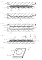
本発明の参考例1について、図1と図5とを参照して説明する。図1(1)−(4)は本参考例に係る光デバイスの生産方法を工程順に示す部分断面図であり、図1(5)は完成したレンズ部材を示す斜視図である。以下に示すいずれの図においても、図5に示された構成要素に対して同一の構成要素については、同一の符号を付して説明を省略する。また、以下の説明では、光素子としてLEDチップを、光デバイスとしてLEDパッケージを、それぞれ例に挙げて説明する。LEDチップに限らず、受けた光を電気的信号に変換する受光素子、例えば、フォトダイオード(PD)、固体撮像素子等のチップに対して本発明を適用することができる。また、受けた電気的信号に応じて発光する発光素子、例えば、レーザダイオード(LD)等のチップに対して本発明を適用することができる。加えて、光通信に使用されるモジュールに対して本発明を適用することができる。すなわち、光素子に対して本発明を適用することができる。 Reference Example 1 of the present invention will be described with reference to FIGS. 1 (1) to 1 (4) are partial cross-sectional views showing the optical device production method according to this reference example in the order of steps, and FIG. 1 (5) is a perspective view showing a completed lens member. In any of the drawings shown below, the same components as those shown in FIG. 5 are denoted by the same reference numerals and description thereof is omitted. In the following description, an LED chip will be described as an example of an optical element, and an LED package will be described as an example of an optical device. The present invention can be applied not only to an LED chip but also to a light receiving element that converts received light into an electrical signal, for example, a chip such as a photodiode (PD) or a solid-state imaging element. In addition, the present invention can be applied to a light emitting element that emits light in accordance with the received electrical signal, for example, a chip such as a laser diode (LD). In addition, the present invention can be applied to modules used for optical communication. That is, the present invention can be applied to optical elements.
本参考例は、基板とLEDチップと保護用部材とを有する半製品(図5(3)の半製品8参照)に接着するレンズ部材、すなわち透光性部材を、複数のレンズ部材を含む成形体を一括して樹脂成形した後にその成形体を分離することによって形成することを特徴とする。本参考例に係る光デバイスの生産方法によれば、まず、図1(1)に示すように、相対向する下型13と上型14とを準備し、下型に設けられたキャビティ15に、透光性を有する熱硬化性樹脂からなる所定量の粒状の樹脂材料16を供給する。キャビティ15には、レンズ部材の形状に応じた複数の凹部が格子状に形成されている。また、樹脂材料16については、図示したような粒状以外に粉状、塊状、シート状でもよく、一定の透光性を有する熱可塑性樹脂を使用してもよい。また、常温で液状である樹脂材料をキャビティ15に注入してもよい。
In this reference example, a lens member that adheres to a semi-finished product (see the
次に、図1(2)に示すように、図1(1)の状態から上型14を下降させて、下型13と上型14とを型締めするとともに樹脂材料16を押圧する。そして、下型13と上型14とに設けられたヒータ(図示なし)を使用して樹脂材料16を加熱し溶融させて、キャビティ15において流動性樹脂17を生成する。その後に、流動性樹脂17を硬化させて、図1(3)に示すように硬化樹脂18からなる成形体19を形成する。これにより、いわゆる圧縮成形を使用して、成形体19を一括して成形したことになる。ここで、トランスファ成形を使用して、成形体19を一括して成形することもできる。
Next, as shown in FIG. 1 (2), the upper mold 14 is lowered from the state of FIG. 1 (1), the lower mold 13 and the upper mold 14 are clamped, and the resin material 16 is pressed. Then, the resin material 16 is heated and melted using heaters (not shown) provided in the lower mold 13 and the upper mold 14 to generate the fluid resin 17 in the
次に、図1(3)に示すように、上型14を上昇させて下型13と上型14とを型開きする。そして、成形体19を取り出した後に、吸着等の手段を使用して成形体19を保持し、次工程で使用される切断装置に搬送する。 Next, as shown in FIG. 1 (3), the upper die 14 is raised to open the lower die 13 and the upper die 14. And after taking out the molded object 19, it hold | maintains the molded object 19 using means, such as adsorption | suction, and conveys it to the cutting device used at the next process.
次に、図1(4)に示すように、適度な粘着性、言い換えれば弱い接着力を有するダイシングシート20を使用して、ステージ21に成形体19を仮固定する。そして、回転刃22を使用して、成形体19に設けられた仮想的なダイシングライン23に沿って、Y方向(図の手前−奥の方向)とX方向(図の左右方向)とに成形体19を切断する。このことにより、成形体19を個片化して、図1(5)に示された透光性部材、すなわち凸レンズとして機能する透光部10と、矩形の平面形状を有する平板状のフランジ部24とを有するレンズ部材25が完成する。この矩形の平面形状を有するレンズ部材25が、本発明に係る透光性部材に相当する。ここで、成形体19を切断して全てのレンズ部材25を形成した後に、全てのレンズ部材25がダイシングシート20に仮固定された状態で搬送、保管、出荷等を行う。
Next, as shown in FIG. 1 (4), the molded body 19 is temporarily fixed to the stage 21 using a
次に、図5(3)と同様にして、半製品8の凹部7に接着剤(図示なし)を塗布する。その後に、レンズ部材25を、吸着等によって保持し、更にダイシングシート20から引き離し搬送して、凹部7に対して位置合わせする。なお、本参考例では、図5に示された凹部7は、図1(5)のフランジ部24に対応する矩形の平面形状を有している。
Next, an adhesive (not shown) is applied to the
次に、図5(4)と同様にして、レンズ部材25を下降させて凹部7の上に載置し、接着剤を硬化させる。これにより、レンズ付半製品(図5(4),(5)のレンズ付半製品12参照)が完成する。以上の工程の後にリードの曲げ加工を行って、本参考例に係る光デバイス(LEDパッケージ)を完成させる。
Next, as in FIG. 5 (4), the
以上説明したように、本参考例によれば、リードフレームに保護用部材とその天面に固定されたレンズ部材25とが設けられた光デバイスに関して、一括して成形された成形体19が個片にそれぞれ分離されることによって形成されたレンズ部材25が使用される。したがって、射出成形等によって個別にレンズ部材を形成する場合に比較して、光デバイスを生産する際に生産効率が向上するとともに、在庫管理、保管、搬送等が簡単になる。また、レンズ部材25は、平板状で広いフランジ部24と矩形の平面形状とを有する。これにより、レンズ部材25のハンドリングを行う際に、フランジ部24を掴み、又はフランジ部24において吸着することができる。また、フランジ部24の面積が小さい場合であっても、その各辺において側面を挟むことによってレンズ部材25を保持することができる。したがって、レンズ部材25をハンドリングする際に、ミスの発生と透光部10に傷がつくことによる品質の低下とが抑制される。
As described above, according to the present reference example, the molded body 19 formed in one batch is individually provided for the optical device in which the lead frame is provided with the protective member and the
なお、本参考例では、回転刃22を使用して成形体19を切断した。これに限らず、成形体19を成形する際にダイシングライン23の位置に溝を形成し、その溝の部分で折り曲げて互いに切り離すことによって、成形体19を個片のレンズ部材25に分離してもよい。
In this reference example, the molded body 19 was cut using the rotary blade 22. Not limited to this, when forming the molded body 19, a groove is formed at the position of the dicing
また、本発明に係る透光性部材として、レンズ部材25を例にとって説明した。これに限らず、鏡筒と一体化されたレンズ部材(図5(3)における、基板1の上側の保護用部材6とレンズ部材9とからなる部分)を、本発明に係る透光性部材としてもよい。
Further, the
本発明の参考例2について、図1と図2とを参照して説明する。図2(1)−(4)は本参考例に係る光デバイスの生産方法を工程順に示す部分断面図であり、図2(5)は光デバイスのレンズ付半製品を示す平面図である。本参考例は、成形体を切断する際にステージに対して成形体を仮固定することと、成形体が切断されることによって個片化されたレンズ部材をレンズ付半製品に接着することとを、1枚の両面接着シートによって行うことを特徴とする。本参考例によれば、まず、図2(1)に示すように、3層構造を有する両面接着シート26を成形体19の下面に貼付する。この両面接着シート26は、基材27と、基材27の一方の面(図では下面)に形成され弱い接着力を有する仮固定用の仮接着層28と、基材27の他方の面(図では上面)に形成され強い接着力を有する本固定用の本接着層29とによって構成されている。そして、両面接着シート26の本接着層29が、成形体19の下面に貼付される。また、1個のレンズ部材25に対応する本接着層29は、フランジ部24の下方に存在し透光部10の下方には存在しないようにして枠状に設けられている。なお、本接着層29として、例えば、アクリル系のような透光性材料を使用した場合には、レンズ部材25の下面全体に本接着層29を設けてもよい。
Reference Example 2 of the present invention will be described with reference to FIGS. FIGS. 2 (1) to (4) are partial cross-sectional views showing the optical device production method according to this reference example in the order of steps, and FIG. 2 (5) is a plan view showing a semi-finished product with a lens of the optical device. In this reference example, when the molded body is cut, the molded body is temporarily fixed to the stage, and the lens member separated by cutting the molded body is bonded to the semi-finished product with a lens. Is performed by one double-sided adhesive sheet. According to this reference example, first, as shown in FIG. 2 (1), the double-sided adhesive sheet 26 having a three-layer structure is attached to the lower surface of the molded body 19. The double-sided adhesive sheet 26 includes a base material 27, a temporary fixing temporary adhesive layer 28 that is formed on one surface (lower surface in the drawing) and has a weak adhesive force, and the other surface of the base material 27 ( It is composed of a
次に、図1(4)に示したダイシングシート20に代えて両面接着シート26を使用して、仮接着層28によってステージ21に成形体19を仮固定する。そして、回転刃22を使用して、ダイシングライン23に沿って成形体19を切断する。
Next, instead of the dicing
次に、切断されることによって個片化されたレンズ部材25を、ステージ21上の仮接着層28から引き剥がす。これにより、図2(2)に示すように、本接着層29と基材27とがこの順で下面に貼着しているレンズ部材25が形成される。
Next, the
次に、図2(3)に示すように、吸着保持具30を使用してフランジ部24を吸着することによって、レンズ部材25を保持して搬送する。そして、図2(4)に示すように、レンズ部材25を、半製品31に対して位置合わせし、下降させて半製品31の上面に接触させ、更に加圧する。これにより、半製品31の上面にレンズ部材25を接着する。その後にリードの曲げ加工を行って、本参考例に係る光デバイス(LEDパッケージ)を完成させる。
Next, as shown in FIG. 2 (3), the
以上説明したように、本参考例によれば、成形体19を切断し個片化する際に使用する仮固定手段と、個片化されたレンズ部材25を半製品31に接着する本固定手段として、1枚の両面接着シート26を使用する。これにより、半製品31に接着剤を塗布する工程を省略することができるので、光デバイスを生産する際の生産効率を向上させることができる。
As described above, according to this reference example, the temporary fixing means used when cutting the molded body 19 into pieces and the permanent fixing means for bonding the separated
本発明の参考例3について、図3を参照して説明する。図3(1)−(4)は本参考例に係る光デバイスの生産方法を工程順に示す部分断面図であり、図3(5)は完成した光デバイスを示す断面図である。本参考例に係る光デバイスの生産方法によれば、まず、図3(1)に示すように、光デバイスに対応する領域32が格子状に形成されたプリント基板等からなる全体基板33を準備する。そして、矩形の平面形状を有する各領域32にチップ3を装着し、ワイヤ4を使用してワイヤボンディングを行う。
Reference Example 3 of the present invention will be described with reference to FIG. 3 (1) to 3 (4) are partial cross-sectional views showing the optical device production method according to this reference example in the order of steps, and FIG. 3 (5) is a cross-sectional view showing the completed optical device. According to the method for producing an optical device according to this reference example, first, as shown in FIG. 3 (1), an entire substrate 33 made of a printed circuit board or the like in which regions 32 corresponding to the optical device are formed in a lattice shape is prepared. To do. Then, the
次に、図3(2)に示すように、各領域32においてチップ3をそれぞれ取り囲む保護用全体部材34を、一括してトランスファ成形することによって形成する。また、この工程では、全体基板33とは無関係に単独にかつ予め一体的に成形した保護用全体部材を、全体基板33に対して位置合わせして接着してもよい。これらの方法によって、全体基板33において保護用全体部材34を一括して設けることができる。
Next, as shown in FIG. 3B, the entire protective member 34 that surrounds the
次に、図3(3)に示すように、透光性樹脂を使用して一括して成形された成形体19を準備する(図1(3)参照)。この成形体19の下面には、予め接着シート35を貼付しておくことが好ましい。この接着シート35は、図2に示された本接着層29と同様の機能を有する。そして、全体基板33に対して成形体19を位置合わせした後に、成形体19を下降させて保護用全体部材34の天面(図では上面)に押圧する。これによって、成形体19と保護用全体部材34とを一括して接着する。
Next, as shown in FIG. 3 (3), a molded body 19 formed in a lump using a translucent resin is prepared (see FIG. 1 (3)). An adhesive sheet 35 is preferably pasted on the lower surface of the molded body 19 in advance. The adhesive sheet 35 has the same function as the main
次に、図3(4)に示すように、成形体19と保護用全体部材34とが接着して形成された中間体36をステージ(図示なし)に仮固定する。そして、回転刃22を使用して、中間体36において仮想的に設けられたダイシングライン23に沿って、Y方向(図の手前−奥の方向)とX方向(図の左右方向)とに中間体36を切断する。これにより、中間体36を各領域32単位に分離して個片化する。
Next, as shown in FIG. 3 (4), an intermediate body 36 formed by bonding the molded body 19 and the protective whole member 34 is temporarily fixed to a stage (not shown). Then, using the rotary blade 22, along the dicing
ここまでの工程により、図3(5)に示されている本参考例に係る光デバイス37(LEDパッケージ)が完成する。この光デバイス37は、全体基板33が個片化された基板38と、基板38の上面に装着されたチップ3と、チップ3を取り囲むようにして設けられた保護用部材39と、保護用部材39の上面に接着された透光性部材であるレンズ部材25とを有する。また、光デバイス37は、基板38の下面に設けられた外部電極(図示なし)によって、他のプリント基板等(図示なし)に電気的に接続される。
Through the steps so far, the optical device 37 (LED package) according to this reference example shown in FIG. This optical device 37 includes a
以上説明したように、本参考例によれば、全体基板33の各領域32に装着されたチップ3を取り囲む保護用全体部材34を一括して成形し、一括して成形され透光性を有する成形体19を保護用全体部材34の上に接着して中間体36を形成し、その中間体36を各領域32単位に分離して光デバイス37を完成させる。したがって、個々の半製品にレンズ部材をそれぞれ接着する生産方法(図5参照)に比較して、光デバイスの生産効率が大幅に向上する。また、光デバイス37が有するレンズ部材25については、中間体が切断されるまでは成形体19として一体的にハンドリングされる。このことにより、成形体19においてレンズ部材25に相当しない部分(周辺の部分)を使用して、成形体19を掴み、又は吸着することができる。したがって、成形体19をハンドリングする際に、ミスの発生とレンズ部材25に傷がつくことによる品質の低下とを防止することができる。また、光デバイス37が矩形の平面形状を有するので、側面を挟むことによって光デバイス37のハンドリングが容易になるとともに、レンズ部材25の傷を防止できる。
As described above, according to the present reference example, the entire protective member 34 surrounding the
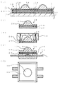
本発明の実施例1について、図4を参照して説明する。図4(1)−(4)は本実施例に係る光デバイスの生産方法を工程順に示す部分断面図であり、図4(5)は完成した光デバイスを示す断面図である。本実施例に係る光デバイスの生産方法によれば、まず、図3(1)に示す場合と同様に、全体基板33の各領域32にチップ3を装着し、ワイヤ4を使用してワイヤボンディングを行う。そして、相対向する下型40と上型41とを準備する。ここで、下型40にはキャビティ42が形成されており、そのキャビティ42には各チップ3に対応する複数の凹部が格子状に形成されている。そして、図4(1)に示すように、吸着などの方法によって上型41に全体基板33を固定する。また、キャビティ42には、図1(1)に示す場合と同様に、透光性を有する熱硬化性樹脂からなる所定量の粒状の樹脂材料43を供給する。
A first embodiment of the present invention will be described with reference to FIG. 4 (1) to 4 (4) are partial cross-sectional views showing the optical device production method according to this embodiment in the order of steps, and FIG. 4 (5) is a cross-sectional view showing the completed optical device. According to the optical device production method of the present embodiment, first, as in the case shown in FIG. 3 (1), the
次に、図4(2)に示すように、樹脂材料43を加熱し溶融させてキャビティ42において流動性樹脂44を生成するとともに、下型40と上型41とを型締めする。ここで、樹脂材料43を加熱するには、下型40に設けられたヒータ(図示なし)を使用する。また、ヒータに代えて、又はヒータに加えて、下型40と上型41との間にそれぞれ挿入された接触式の加熱板や非接触式のハロゲンランプ等を使用してもよい。 Next, as shown in FIG. 4 (2), the resin material 43 is heated and melted to produce a fluid resin 44 in the cavity 42, and the lower mold 40 and the upper mold 41 are clamped. Here, in order to heat the resin material 43, a heater (not shown) provided in the lower mold 40 is used. Further, instead of or in addition to the heater, a contact type heating plate or a non-contact type halogen lamp inserted between the lower mold 40 and the upper mold 41 may be used.
次に、図4(3)に示すように、流動性樹脂44を硬化させて硬化樹脂からなる成形体45を形成するとともに全体基板33と成形体45とを有する中間体46を形成し、その後に、上型41を上昇させて下型(図示なし)と上型41とを型開きする。この成形体45は、全体基板33において各チップ3を一括して封止する封止用全体部材として機能する。ここまでの工程により、圧縮成形を使用して、中間体46を一括して成形したことになる。なお、圧縮成形に代えてトランスファ成形を使用して、硬化樹脂を形成するとともに中間体46を一括して成形することもできる。
Next, as shown in FIG. 4 (3), the fluid resin 44 is cured to form a molded body 45 made of a cured resin, and an intermediate body 46 having the entire substrate 33 and the molded body 45 is formed. Then, the upper mold 41 is raised to open the lower mold (not shown) and the upper mold 41. The molded body 45 functions as an entire sealing member that collectively seals the
次に、図4(4)に示すように、中間体46をステージ(図示なし)に仮固定する。そして、回転刃22を使用して、中間体46において仮想的に設けられたダイシングライン23に沿って、Y方向(図の手前−奥の方向)とX方向(図の左右方向)とに中間体46を切断する。これにより、中間体46を各領域32単位に分離して個片化する。
Next, as shown in FIG. 4 (4), the intermediate body 46 is temporarily fixed to a stage (not shown). And using the rotary blade 22, along the dicing
ここまでの工程により、図4(5)に示されている本実施例に係る光デバイス47(LEDパッケージ)が完成する。この光デバイス47は、全体基板33が個片化された基板38と、基板38の上面に装着されたチップ(図示なし)と、凸レンズ状の透光部48及び平板状のフランジ部49を有するとともにチップを封止する透光性部材、すなわちレンズ部材50とを備えている。
Through the steps so far, the optical device 47 (LED package) according to the present embodiment shown in FIG. The optical device 47 includes a
以上説明したように、本実施例によれば、全体基板33の各領域32に装着されたチップ3を一括して封止して中間体46を成形し、その中間体46を各領域32単位に分離して光デバイス47を完成させる。これにより、個々の半製品にレンズ部材を接着する生産方法(図5参照)に比較して、光デバイスの生産効率がいっそう大幅に向上する。また、保護用部材を形成する生産方法(図3参照)に比較して、生産効率が向上する。加えて、中間体46においてレンズ部材50に相当しない部分(成形体45における周辺の部分)を使用して、中間体46を掴み、又は吸着することができる。したがって、中間体46をハンドリングする際に、ミスの発生とレンズ部材50に傷がつくことによる品質の低下とを防止することができる。また、光デバイス47が矩形の平面形状を有するので、側面を挟むことによって光デバイス47のハンドリングが容易になるとともに、レンズ部材50の傷を防止できる。
As described above, according to the present embodiment, the
なお、本実施例においては、全体基板33と硬化樹脂からなる成形体45とを有する中間体46を一括して成形した。これに代えて、透光性樹脂を使用して、硬化樹脂からなる部分に代わる部材を予め一体的に成形しておき、成形されたその部材を封止用全体部材として使用してもよい。この場合には、まず、封止用全体部材を、全体基板33とは無関係に単独にかつ予め一体的に成形する。具体的には、成形体45のうちLEDチップ3及びワイヤ4の周囲における所定の空間を除いた部分、言い換えれば、図3(4)に示された成形体19と保護用全体部材34とに相当する部分を、封止用全体部材として一括して成形する。次に、全体基板33に対してその封止用全体部材を位置合わせして接着する。これにより、保護用部材とレンズ部材として機能する封止用全体部材を全体基板33の上に一括して設けて、中間体を形成することができる。次に、その中間体を各領域32単位に分離して個片化する。こうして得られた光デバイスは、図3(5)に示されたレンズ部材25と保護用部材39とが一体化しているとともに透光性樹脂からなる構成を有する。
In this embodiment, the intermediate body 46 having the entire substrate 33 and the molded body 45 made of a cured resin is molded in a lump. Instead of this, a member that replaces the portion made of the cured resin may be integrally formed in advance using a translucent resin, and the formed member may be used as the entire sealing member. In this case, first, the whole sealing member is integrally formed in advance independently and independently of the whole substrate 33. Specifically, a portion of the molded body 45 excluding a predetermined space around the
なお、参考例1−3と実施例1とにおいては、レンズ部材25,50が凸レンズ状の透光部10,48と平板状のフランジ部24,49とを有することとした。これに限らず、レンズ部材25,50の全体が凸レンズ状の透光部になるようにして形成してもよい。この場合には、切断後にダイシングシート(図1(4)のダイシングシート20を参照)をエキスパンドした状態で、レンズ部材25,50の側面又は光デバイス37,47の側面、すなわち凸レンズ状の透光部以外の部分を掴むことができる。これにより、レンズ部材25,50と光デバイス37,47とをそれぞれハンドリングする際に、ミスの発生と品質の低下とを防止することができる。
In Reference Example 1-3 and Example 1, the
また、チップと基板とが有する電極同士の電気的接続に、ワイヤボンディングを使用した。これに代えて、他の接続方法を使用してもよい。例えば、基板に設けられた開口を通して発光又は受光するようにして、チップをフリップチップボンディングしてもよい。 Further, wire bonding was used for electrical connection between electrodes of the chip and the substrate. Alternatively, other connection methods may be used. For example, the chip may be flip-chip bonded so as to emit or receive light through an opening provided in the substrate.
また、回転刃22を使用して、成形体19、中間体36,46をそれぞれ切断した。これに限らず、レーザによる切断(溶断)、ワイヤソー等による切断を使用してもよい。 Moreover, the molded object 19 and the intermediate bodies 36 and 46 were each cut | disconnected using the rotary blade 22. FIG. However, the present invention is not limited to this, and laser cutting (melting), cutting with a wire saw or the like may be used.
また、レンズ部材25については、光デバイスの外側に凸になるようにして配置した。これに限らず、光デバイスの内側に凸になるようにレンズ部材25を配置してもよい。また、レンズ部材25の形状としては、両面に凸になるような形状にしてもよく、凸レンズ状の透光部とその周囲に設けられた光反射壁とを有する形状にしてもよい。これらの点については、参考例3の成形体19と実施例1のなお書きにおける封止用全体部材とにおいても同様である。
Further, the
また、例えば、ある種の受光素子等のようにレンズ部材を必要としない場合には、透光性部材として平板状の部材を使用してもよい。また、平板状の成形体を一括して成形し、これを保護用全体部材に接着して中間体を形成した後に、中間体を分離して個片の光デバイスを完成させてもよい(図3(3),(4)参照)。更に、図4に示されたレンズ部材50に代えて、平板状の部材を有することとしてもよい。これらの場合には、その平板状の部材が、本発明に係る透光性部材に相当する。 Further, for example, when a lens member is not required as in a certain type of light receiving element or the like, a flat plate member may be used as the translucent member. Alternatively, a flat molded body may be molded in a lump and bonded to the entire protective member to form an intermediate body, and then the intermediate body may be separated to complete an individual optical device (see FIG. 3 (3), (4)). Furthermore, it is good also as replacing with the lens member 50 shown by FIG. 4 and having a flat member. In these cases, the flat plate member corresponds to the translucent member according to the present invention.
また、光デバイスが受光素子を有する場合、又は、光デバイスが発光素子と受光素子との双方を有する場合においても、本発明を適用することができる。 The present invention can also be applied when the optical device has a light receiving element or when the optical device has both a light emitting element and a light receiving element.
また、本発明は、上述の実施例1に限定されるものではなく、本発明の趣旨を逸脱しない範囲内で、必要に応じて、任意にかつ適宜に組み合わせ、変更し、又は選択して採用できるものである。 Further, the present invention is not limited to the above-described first embodiment, and may be arbitrarily combined, changed, or selected as necessary without departing from the spirit of the present invention. It can be done.
1 リードフレーム(基板)
2 上面
3 LEDチップ(チップ)
4 ワイヤ
5 下面
6,39 保護用部材
7 凹部
8,31 半製品
9 レンズ部材
10 透光部
11,24 フランジ部
12 レンズ付半製品
13,40 下型
14,41 上型
15,42 キャビティ
16,43 樹脂材料
17,44 流動性樹脂
18 硬化樹脂
19 成形体
20 ダイシングシート
21 ステージ
22 回転刃
23 ダイシングライン
25,50 レンズ部材(封止用部材)
26 両面接着シート
27 基材
28 仮接着層
29 本接着層
30 吸着保持具
32 領域
33 全体基板
34 保護用全体部材
35 接着シート
36,46 中間体
37,47 光デバイス
38 基板
45 成形体(封止用全体部材)
48 透光部(レンズ部材)
49 フランジ部
1 Lead frame (substrate)
2
4
26 Double-sided adhesive sheet 27 Base material 28
48 Translucent part (lens member)
49 Flange
Claims (12)
前記基板に各々対応するように格子状に形成された複数の領域を有する全体基板と、前記複数の領域における前記一方の面に各々装着された前記チップと、前記複数の領域に各々対応する前記封止用部材を有し前記全体基板上において一括して成形された封止用全体部材とからなる中間体が、前記各領域単位に格子状に切断されることによって形成され、
前記チップと前記基板とが各々有する電極同士がワイヤボンディング又はフリップチップボンディングによって電気的に接続されるとともに、
前記封止用全体部材は、相対向する上型と下型とからなる成形型のうち前記下型が有するキャビティにおいて、圧縮成形によって前記一方の面の側において一括して成形された硬化樹脂からなり、
前記中間体における前記硬化樹脂は、前記全体基板が有する他方の面が前記上型に固定された状態で、前記成形型が型開きした状態において前記キャビティに供給された固体状の樹脂材料が溶融して生成された流動性樹脂に前記成形型が型締めすることによって前記チップが完全に浸漬した状態で、又は、前記成形型が型開きした状態において前記キャビティに供給された常温で液状である樹脂材料に前記成形型が型締めすることによって前記チップが完全に浸漬した状態で、前記流動性樹脂又は前記常温で液状である樹脂材料が前記成形型に設けられた加熱手段によって加熱されて硬化することによって形成され、
前記チップは前記硬化樹脂によって隙間無く覆われており、
前記硬化樹脂からなり、レンズとして機能する透光部を有するレンズ部材と、
前記硬化樹脂からなり、前記透光部の周囲における平面視して前記基板の全ての範囲に形成された平板状のフランジ部とを備えることを特徴とする光デバイス。 An optical device comprising a substrate, a chip made of an optical element mounted on one surface of the substrate, and a light-transmitting sealing member provided on the substrate for sealing the chip There,
An entire substrate having a plurality of regions formed in a lattice shape so as to correspond to each of the substrates, the chip mounted on each of the one surface in the plurality of regions, and the corresponding to each of the plurality of regions An intermediate body composed of a sealing whole member formed in a lump on the whole substrate having a sealing member is formed by being cut into a lattice shape in each region unit,
While the electrodes each of the chip and the substrate are electrically connected by wire bonding or flip chip bonding,
The whole sealing member is made of a cured resin that is collectively molded on the one surface side by compression molding in a cavity of the lower mold among the molds composed of the upper mold and the lower mold facing each other. Become
The cured resin in the intermediate body melts the solid resin material supplied to the cavity in a state where the mold is opened while the other surface of the entire substrate is fixed to the upper mold. The mold is clamped in the flowable resin produced in the above state so that the chip is completely immersed, or the mold is in a liquid state at normal temperature supplied to the cavity when the mold is opened. The mold is clamped in a resin material, and the chip is completely immersed, and the fluid resin or the resin material that is liquid at room temperature is heated and cured by heating means provided in the mold. Formed by
The chip is covered with the cured resin without a gap,
A lens member made of the cured resin and having a translucent part that functions as a lens;
An optical device comprising: a flat flange portion made of the cured resin and formed in the entire range of the substrate in a plan view around the translucent portion.
前記フランジ部は、前記キャビティにおいて前記複数の領域に各々対応して設けられた複数の凹部同士を連通する連通部において前記複数の凹部の間を互いに流動する前記流動性樹脂又は前記常温で液状である樹脂材料が硬化することによって形成され、
前記レンズ部材は、前記キャビティにおいて前記複数の領域に各々対応して設けられた複数の凹部において前記流動性樹脂又は前記常温で液状である樹脂材料が硬化することによって形成されたことを特徴とする光デバイス。 The optical device according to claim 1.
The flange portion is a liquid at the normal temperature or the fluid resin that flows between the plurality of recesses in a communication portion that communicates the plurality of recesses provided corresponding to the plurality of regions in the cavity. A resin material is formed by curing,
The lens member is formed by curing the flowable resin or the resin material that is liquid at room temperature in a plurality of recesses provided in the cavity corresponding to the plurality of regions, respectively. Optical device.
前記レンズ部材は前記チップに各々対応する凸レンズ状の透光部を有することを特徴とする光デバイス。 The optical device according to claim 1 or 2,
The optical device is characterized in that the lens member has a convex lens-shaped light transmitting portion corresponding to each of the chips.
前記硬化樹脂からなる平板状の透光部を有することを特徴とする光デバイス。 The optical device according to claim 1 or 2,
An optical device comprising a flat light-transmitting portion made of the cured resin.
前記中間体が回転刃、レーザ光、又はワイヤソーのいずれかを使用して個片化されることによって形成されることを特徴とする光デバイス。 In the optical device in any one of Claims 1-4,
An optical device, wherein the intermediate body is formed by singulation using any one of a rotary blade, a laser beam, and a wire saw.
前記光デバイスが有する側面を挟むことによってハンドリングされることを特徴とする光デバイス。 In the optical device in any one of Claims 1-5,
The optical device is handled by sandwiching a side surface of the optical device.
前記基板に各々対応するように格子状に形成された複数の領域を有するとともに該複数の領域における前記一方の面に前記チップが各々装着された全体基板を準備する工程と、
相対向する上型と下型とからなる成形型のうち前記上型に前記全体基板における他方の面を固定する工程と、
前記全体基板において、複数個の前記封止用部材を有する封止用全体部材を一括して成形する工程と、
前記封止用全体部材を一括して成形する工程によって形成された中間体を前記各領域単位に格子状に切断する工程とを備えるとともに、
前記封止用全体部材を一括して成形する工程は、
前記下型が有するキャビティを流動性樹脂によって満たされた状態にする工程と、
前記成形型を型締めすることによって前記チップを前記流動性樹脂の中に完全に浸漬する工程と、
前記成形型に設けられた加熱手段によって前記流動性樹脂を加熱して硬化させて硬化樹脂を一括して圧縮成形することによって、前記一方の面の側において前記硬化樹脂からなる前記封止用全体部材を成形する工程とを有し、
前記封止用全体部材を成形する工程では、
前記硬化樹脂によって前記チップを隙間無く覆い、
各々前記硬化樹脂からなり、レンズとして機能する透光部と、互いに隣接する前記透光部同士を該透光部同士の間における平面視して前記基板の全ての範囲において連通させる平板状のフランジ部とを形成することを特徴とする光デバイスの生産方法。 An optical device comprising a substrate, a chip made of an optical element mounted on one surface of the substrate, and a translucent sealing member provided on the substrate for sealing the chip A production method,
Preparing a whole substrate having a plurality of regions formed in a lattice shape so as to correspond to each of the substrates and having the chips mounted on the one surface in the plurality of regions;
Fixing the other surface of the whole substrate to the upper mold among the molds composed of the upper mold and the lower mold facing each other;
In the whole substrate, a step of collectively molding a whole sealing member having a plurality of the sealing members;
And a step of cutting the intermediate formed by the step of collectively molding the whole sealing member into a lattice shape in each region unit,
The step of collectively molding the whole sealing member,
A step of filling the cavity of the lower mold with a fluid resin;
Completely immersing the chip in the flowable resin by clamping the mold; and
The whole sealing material made of the cured resin on the one surface side by heating and curing the fluid resin by a heating means provided in the mold and collectively compressing the cured resin. Forming a member,
In the step of molding the whole sealing member,
Cover the chip with the cured resin without gaps,
Each of the curable resins and a flat plate-shaped flange that communicates with each other in the entire range of the substrate in a plan view between the light-transmitting portions adjacent to each other. And a method of producing an optical device.
前記キャビティにおいて前記複数の領域に各々対応して設けられた複数の凹部同士を連通する連通部において、前記複数の凹部の間を互いに流動する前記流動性樹脂又は前記常温で液状である樹脂材料を硬化させることによって、前記フランジ部を形成することを特徴とする光デバイスの生産方法。 The method for producing an optical device according to claim 7,
In the communication portion that communicates the plurality of recesses provided corresponding to the plurality of regions in the cavity, the flowable resin that flows between the plurality of recesses or the resin material that is liquid at room temperature. A method for producing an optical device, wherein the flange portion is formed by curing.
前記キャビティを流動性樹脂によって満たされた状態にする工程では、前記成形型が型開きした状態において前記キャビティに供給された固体状の樹脂材料を溶融させることによって前記流動性樹脂を生成することを特徴とする光デバイスの生産方法。 The method for producing an optical device according to claim 7 or 8,
In the step of filling the cavity with the fluid resin, the fluid resin is generated by melting the solid resin material supplied to the cavity in a state where the mold is opened. A featured optical device production method.
前記キャビティを流動性樹脂によって満たされた状態にする工程では、前記成形型が型開きした状態において常温で液状である樹脂材料を前記キャビティに供給することを特徴とする光デバイスの生産方法。 The method for producing an optical device according to claim 7 or 8,
In the step of filling the cavity with a flowable resin, a resin material that is liquid at room temperature in a state where the mold is opened is supplied to the cavity.
前記切断する工程では、回転刃、レーザ光、又はワイヤソーのいずれかを使用して前記中間体を前記光デバイスに切断することを特徴とする光デバイスの生産方法。 In the manufacturing method of the optical device in any one of Claims 7-10,
In the cutting step, the intermediate body is cut into the optical device using any one of a rotary blade, a laser beam, and a wire saw.
前記切断する工程の後に、前記光デバイスが有する側面を挟むことによって前記光デバイスをハンドリングする工程を備えることを特徴とする光デバイスの生産方法。 In the manufacturing method of the optical device in any one of Claims 7-11,
A method for producing an optical device comprising the step of handling the optical device by sandwiching a side surface of the optical device after the cutting step.
Priority Applications (5)
| Application Number | Priority Date | Filing Date | Title |
|---|---|---|---|
| JP2004294980A JP5128047B2 (en) | 2004-10-07 | 2004-10-07 | Optical device and optical device production method |
| TW094133496A TWI274657B (en) | 2004-10-07 | 2005-09-27 | Transparent member, optical device using transparent member and method of manufacturing optical device |
| US11/243,967 US20060078246A1 (en) | 2004-10-07 | 2005-10-06 | Transparent member, optical device using transparent member and method of manufacturing optical device |
| US11/480,377 US7682853B2 (en) | 2004-10-07 | 2006-07-05 | Transparent member, optical device using transparent member and method of manufacturing optical device |
| US12/163,669 US8222059B2 (en) | 2004-10-07 | 2008-06-27 | Method transparent member, optical device using transparent member and method of manufacturing optical device |
Applications Claiming Priority (1)
| Application Number | Priority Date | Filing Date | Title |
|---|---|---|---|
| JP2004294980A JP5128047B2 (en) | 2004-10-07 | 2004-10-07 | Optical device and optical device production method |
Related Child Applications (2)
| Application Number | Title | Priority Date | Filing Date |
|---|---|---|---|
| JP2011115422A Division JP2011171765A (en) | 2011-05-24 | 2011-05-24 | Optical device and method for assembling the same |
| JP2011115421A Division JP2011187979A (en) | 2011-05-24 | 2011-05-24 | Entire substrate with protecting entire member, and method of manufacturing the same |
Publications (3)
| Publication Number | Publication Date |
|---|---|
| JP2006106479A JP2006106479A (en) | 2006-04-20 |
| JP2006106479A5 JP2006106479A5 (en) | 2007-06-14 |
| JP5128047B2 true JP5128047B2 (en) | 2013-01-23 |
Family
ID=36145415
Family Applications (1)
| Application Number | Title | Priority Date | Filing Date |
|---|---|---|---|
| JP2004294980A Active JP5128047B2 (en) | 2004-10-07 | 2004-10-07 | Optical device and optical device production method |
Country Status (3)
| Country | Link |
|---|---|
| US (3) | US20060078246A1 (en) |
| JP (1) | JP5128047B2 (en) |
| TW (1) | TWI274657B (en) |
Families Citing this family (97)
| Publication number | Priority date | Publication date | Assignee | Title |
|---|---|---|---|---|
| US7344902B2 (en) * | 2004-11-15 | 2008-03-18 | Philips Lumileds Lighting Company, Llc | Overmolded lens over LED die |
| US9070850B2 (en) * | 2007-10-31 | 2015-06-30 | Cree, Inc. | Light emitting diode package and method for fabricating same |
| JP4741383B2 (en) * | 2006-02-17 | 2011-08-03 | 富士通セミコンダクター株式会社 | Resin sealing method for electronic parts |
| US20070216047A1 (en) * | 2006-03-20 | 2007-09-20 | Heptagon Oy | Manufacturing an optical element |
| US20070216046A1 (en) * | 2006-03-20 | 2007-09-20 | Heptagon Oy | Manufacturing miniature structured elements with tool incorporating spacer elements |
| US20070216049A1 (en) * | 2006-03-20 | 2007-09-20 | Heptagon Oy | Method and tool for manufacturing optical elements |
| US20070216048A1 (en) * | 2006-03-20 | 2007-09-20 | Heptagon Oy | Manufacturing optical elements |
| KR100789951B1 (en) * | 2006-06-09 | 2008-01-03 | 엘지전자 주식회사 | Apparatus and method for manufacturing Light Emitting Unit |
| US20100072640A1 (en) * | 2006-06-09 | 2010-03-25 | Heptagon Oy | Manufacturing a replication tool, sub-master or replica |
| DE102006039705A1 (en) * | 2006-08-18 | 2008-02-28 | Schott Ag | Lens attachment for a headlight |
| JP2008205149A (en) * | 2007-02-20 | 2008-09-04 | Towa Corp | Luminous member formation method and mold |
| TWI351115B (en) | 2007-05-18 | 2011-10-21 | Everlight Electronics Co Ltd | Light-emitting diode module and the manufacturing method thereof |
| JP2009047949A (en) * | 2007-08-21 | 2009-03-05 | Alps Electric Co Ltd | Manufacturing method of optical element |
| EP2184626A4 (en) * | 2007-08-28 | 2011-06-15 | Sharp Kk | Method for manufacturing optical member, parent material for manufacture of optical member, transfer mold, lighting system for display device, display device, and television receiver |
| JP2009117536A (en) * | 2007-11-05 | 2009-05-28 | Towa Corp | Resin-sealed light emitter, and manufacturing method thereof |
| WO2009093228A2 (en) * | 2008-01-21 | 2009-07-30 | Prime Sense Ltd. | Optical designs for zero order reduction |
| US8384997B2 (en) | 2008-01-21 | 2013-02-26 | Primesense Ltd | Optical pattern projection |
| DE102008014927A1 (en) | 2008-02-22 | 2009-08-27 | Osram Opto Semiconductors Gmbh | Method for producing a plurality of radiation-emitting components and radiation-emitting component |
| US8461613B2 (en) * | 2008-05-27 | 2013-06-11 | Interlight Optotech Corporation | Light emitting device |
| TWI384651B (en) * | 2008-08-20 | 2013-02-01 | Au Optronics Corp | A light emitting diodes structure and a light emitting diodes structure forming method |
| WO2010050304A1 (en) | 2008-10-31 | 2010-05-06 | コニカミノルタオプト株式会社 | Wafer lens and method for production thereof |
| JP2010123620A (en) * | 2008-11-17 | 2010-06-03 | Stanley Electric Co Ltd | Manufacturing method of semiconductor device |
| JP5327042B2 (en) * | 2009-03-26 | 2013-10-30 | 豊田合成株式会社 | LED lamp manufacturing method |
| US10119662B2 (en) | 2009-04-28 | 2018-11-06 | Cree, Inc. | Lens with controlled light refraction |
| US9915409B2 (en) | 2015-02-19 | 2018-03-13 | Cree, Inc. | Lens with textured surface facilitating light diffusion |
| US9416926B2 (en) | 2009-04-28 | 2016-08-16 | Cree, Inc. | Lens with inner-cavity surface shaped for controlled light refraction |
| US10422503B2 (en) | 2009-10-30 | 2019-09-24 | Ideal Industries Lighting Llc | One-piece multi-lens optical member and method of manufacture |
| US8434883B2 (en) | 2009-05-11 | 2013-05-07 | SemiOptoelectronics Co., Ltd. | LLB bulb having light extracting rough surface pattern (LERSP) and method of fabrication |
| US20120086035A1 (en) * | 2009-05-11 | 2012-04-12 | SemiLEDs Optoelectronics Co., Ltd. | LED Device With A Light Extracting Rough Structure And Manufacturing Methods Thereof |
| US8348461B2 (en) * | 2009-10-30 | 2013-01-08 | Ruud Lighting, Inc. | LED apparatus and method for accurate lens alignment |
| US9404634B2 (en) | 2009-10-30 | 2016-08-02 | Cree, Inc. | LED light fixture with facilitated lensing alignment and method of manufacture |
| US9028097B2 (en) | 2009-10-30 | 2015-05-12 | Cree, Inc. | LED apparatus and method for accurate lens alignment |
| TW201116400A (en) * | 2009-11-09 | 2011-05-16 | Forward Electronics Co Ltd | Method for forming fluorescent glue layer of light emitting diode |
| JP5588310B2 (en) * | 2009-11-15 | 2014-09-10 | プライムセンス リミテッド | Optical projector with beam monitor |
| JP5512262B2 (en) * | 2009-12-26 | 2014-06-04 | 株式会社朝日ラバー | Lens array sheet and dicing method thereof |
| US20110188054A1 (en) * | 2010-02-02 | 2011-08-04 | Primesense Ltd | Integrated photonics module for optical projection |
| US20110187878A1 (en) | 2010-02-02 | 2011-08-04 | Primesense Ltd. | Synchronization of projected illumination with rolling shutter of image sensor |
| JPWO2011102056A1 (en) * | 2010-02-19 | 2013-06-17 | コニカミノルタアドバンストレイヤー株式会社 | Imaging lens unit |
| US9036158B2 (en) | 2010-08-11 | 2015-05-19 | Apple Inc. | Pattern projector |
| US9098931B2 (en) | 2010-08-11 | 2015-08-04 | Apple Inc. | Scanning projectors and image capture modules for 3D mapping |
| EP2643659B1 (en) | 2010-11-19 | 2019-12-25 | Apple Inc. | Depth mapping using time-coded illumination |
| US9131136B2 (en) | 2010-12-06 | 2015-09-08 | Apple Inc. | Lens arrays for pattern projection and imaging |
| JP5562273B2 (en) | 2011-03-02 | 2014-07-30 | Towa株式会社 | Optoelectronic component manufacturing method and manufacturing apparatus |
| CN102694081B (en) * | 2011-03-21 | 2014-11-05 | 展晶科技(深圳)有限公司 | Method for manufacturing light emitting diode |
| DE202011000852U1 (en) * | 2011-04-12 | 2011-06-09 | Flextronics Automotive GmbH & Co.KG, 72636 | LED light |
| JP5316911B2 (en) * | 2011-06-24 | 2013-10-16 | カシオ計算機株式会社 | Light source device and projector |
| US20130037931A1 (en) * | 2011-08-08 | 2013-02-14 | Leo M. Higgins, III | Semiconductor package with a heat spreader and method of making |
| US8908277B2 (en) | 2011-08-09 | 2014-12-09 | Apple Inc | Lens array projector |
| US8749796B2 (en) | 2011-08-09 | 2014-06-10 | Primesense Ltd. | Projectors of structured light |
| JP5658108B2 (en) * | 2011-08-23 | 2015-01-21 | Towa株式会社 | Manufacturing method and manufacturing apparatus for substrate with reflector |
| DE102011113483B4 (en) | 2011-09-13 | 2023-10-19 | OSRAM Opto Semiconductors Gesellschaft mit beschränkter Haftung | Method for producing a plurality of optoelectronic components and optoelectronic component |
| KR101284796B1 (en) * | 2011-10-05 | 2013-07-10 | (주)포인트엔지니어링 | method for light emitting device with can package and the light emitting device |
| CN103165763B (en) * | 2011-12-14 | 2015-07-08 | 赛恩倍吉科技顾问(深圳)有限公司 | Manufacture method of light emitting diode (LED) |
| RU2617880C2 (en) * | 2012-02-10 | 2017-04-28 | Конинклейке Филипс Н.В. | Moulded lens forming led-module of integrated circuit scale and manufacturing method thereof |
| US9157790B2 (en) | 2012-02-15 | 2015-10-13 | Apple Inc. | Integrated optoelectronic modules with transmitter, receiver and beam-combining optics for aligning a beam axis with a collection axis |
| US9329080B2 (en) | 2012-02-15 | 2016-05-03 | Aplle Inc. | Modular optics for scanning engine having beam combining optics with a prism intercepted by both beam axis and collection axis |
| JP5867817B2 (en) * | 2012-02-21 | 2016-02-24 | セイコーインスツル株式会社 | Optical device manufacturing method |
| US9618185B2 (en) | 2012-03-08 | 2017-04-11 | Flextronics Ap, Llc | LED array for replacing flourescent tubes |
| WO2013140308A1 (en) | 2012-03-22 | 2013-09-26 | Primesense Ltd. | Diffraction-based sensing of mirror position |
| US9356214B2 (en) | 2012-06-27 | 2016-05-31 | Flextronics Ap, Llc. | Cooling system for LED device |
| US9366394B2 (en) | 2012-06-27 | 2016-06-14 | Flextronics Ap, Llc | Automotive LED headlight cooling system |
| US20140003777A1 (en) * | 2012-07-02 | 2014-01-02 | Commscope, Inc. Of North Carolina | Light focusing structures for fiber optic communications systems and methods of fabricating the same using semiconductor processing and micro-machining techniques |
| JP6078846B2 (en) * | 2012-11-06 | 2017-02-15 | アピックヤマダ株式会社 | LED mounted product manufacturing method, LED mounted product resin molding method, and LED manufacturing apparatus |
| US10400984B2 (en) | 2013-03-15 | 2019-09-03 | Cree, Inc. | LED light fixture and unitary optic member therefor |
| JP6182916B2 (en) | 2013-03-15 | 2017-08-23 | 日亜化学工業株式会社 | Method for removing sealing member of light emitting device |
| US9920901B2 (en) | 2013-03-15 | 2018-03-20 | Cree, Inc. | LED lensing arrangement |
| KR101827180B1 (en) | 2013-06-19 | 2018-02-07 | 애플 인크. | Integrated structured-light projector |
| CN104347785A (en) * | 2013-08-07 | 2015-02-11 | 广州众恒光电科技有限公司 | Die-method fluorescent powder adhesive layer coating process |
| JP2013225713A (en) * | 2013-08-08 | 2013-10-31 | Towa Corp | Production method of optical device |
| US9395067B2 (en) | 2013-10-07 | 2016-07-19 | Flextronics Ap, Llc | Method of and apparatus for enhanced thermal isolation of low-profile LED lighting fixtures |
| WO2015063370A1 (en) * | 2013-11-04 | 2015-05-07 | Ledil Oy | Light guide with grooves for dividing by bending |
| US9528906B1 (en) | 2013-12-19 | 2016-12-27 | Apple Inc. | Monitoring DOE performance using total internal reflection |
| WO2015110927A1 (en) | 2014-01-23 | 2015-07-30 | Koninklijke Philips N.V. | Light emitting device with self-aligning preformed lens |
| JP6338409B2 (en) * | 2014-03-14 | 2018-06-06 | アルパッド株式会社 | Light emitting device and manufacturing method thereof |
| KR101572495B1 (en) * | 2014-08-20 | 2015-12-02 | 주식회사 루멘스 | Manufacturing method for light emitting device package, alignment jig for light emitting device package, lead-frame strip for light emitting device package and lens strip for light emitting device package |
| US9757912B2 (en) | 2014-08-27 | 2017-09-12 | Cree, Inc. | One-piece multi-lens optical member with ultraviolet inhibitor and method of manufacture |
| US10207440B2 (en) | 2014-10-07 | 2019-02-19 | Cree, Inc. | Apparatus and method for formation of multi-region articles |
| DE102014115622A1 (en) * | 2014-10-28 | 2016-05-12 | Osram Opto Semiconductors Gmbh | Production of a lighting module for a backlight device |
| US9470394B2 (en) | 2014-11-24 | 2016-10-18 | Cree, Inc. | LED light fixture including optical member with in-situ-formed gasket and method of manufacture |
| KR102322336B1 (en) * | 2015-02-06 | 2021-11-05 | 쑤저우 레킨 세미컨덕터 컴퍼니 리미티드 | Light emitting device package and lighting apparatus including the package |
| EP3096167A1 (en) * | 2015-05-18 | 2016-11-23 | OSRAM GmbH | A method of producing lighting devices and optical component for use therein |
| US10012831B2 (en) | 2015-08-03 | 2018-07-03 | Apple Inc. | Optical monitoring of scan parameters |
| US20170075205A1 (en) * | 2015-09-13 | 2017-03-16 | Apple Inc. | Integrated light pipe for optical projection |
| KR102396332B1 (en) | 2015-09-22 | 2022-05-12 | 삼성전자주식회사 | Fine interval coating member for led dispaly and coating method using the same |
| US10073004B2 (en) | 2016-09-19 | 2018-09-11 | Apple Inc. | DOE defect monitoring utilizing total internal reflection |
| US20180182939A1 (en) * | 2016-12-22 | 2018-06-28 | Rayvio Corporation | Package for an ultraviolet emitting device |
| US20180323354A1 (en) * | 2017-05-07 | 2018-11-08 | Yang Wang | Light emitting device and method for manufacturing light emitting device |
| US10153614B1 (en) | 2017-08-31 | 2018-12-11 | Apple Inc. | Creating arbitrary patterns on a 2-D uniform grid VCSEL array |
| WO2019091328A1 (en) * | 2017-11-08 | 2019-05-16 | 厦门市三安光电科技有限公司 | Ultraviolet led packaging structure |
| US11422292B1 (en) | 2018-06-10 | 2022-08-23 | Apple Inc. | Super-blazed diffractive optical elements with sub-wavelength structures |
| TW202002335A (en) * | 2018-06-12 | 2020-01-01 | 同欣電子工業股份有限公司 | Optical device and a method for manufacturing the same |
| US10667341B1 (en) | 2018-09-16 | 2020-05-26 | Apple Inc. | Light projector with integrated integrity sensor |
| CN109216532B (en) * | 2018-11-01 | 2023-09-12 | 上海悦威电子设备有限公司 | Ultraviolet LED quartz lens assembly structure and method |
| US11681019B2 (en) | 2019-09-18 | 2023-06-20 | Apple Inc. | Optical module with stray light baffle |
| US11506762B1 (en) | 2019-09-24 | 2022-11-22 | Apple Inc. | Optical module comprising an optical waveguide with reference light path |
| US11754767B1 (en) | 2020-03-05 | 2023-09-12 | Apple Inc. | Display with overlaid waveguide |
| WO2023007616A1 (en) * | 2021-07-28 | 2023-02-02 | オリンパス株式会社 | Production method for lens unit, lens unit, imaging device, and endoscope |
Family Cites Families (84)
| Publication number | Priority date | Publication date | Assignee | Title |
|---|---|---|---|---|
| US2796634A (en) | 1953-12-21 | 1957-06-25 | Ibm | Reverse forming process for making shaped articles from plastic sheet material |
| JPS611067A (en) | 1984-06-13 | 1986-01-07 | Stanley Electric Co Ltd | Molding method of led chip mounted on printed board |
| US5238640A (en) | 1984-12-10 | 1993-08-24 | Sumitomo Chemical Co., Limited | Method of manufacturing a laminated body |
| US4944908A (en) | 1988-10-28 | 1990-07-31 | Eaton Corporation | Method for forming a molded plastic article |
| US5169677A (en) | 1989-10-27 | 1992-12-08 | Brother Kogyo Kabushiki Kaisha | Method for forming lens at end portion of optical apparatus, optical signal transmission apparatus, and optical information processing apparatus |
| US5147821A (en) | 1990-09-28 | 1992-09-15 | Motorola, Inc. | Method for making a thermally enhanced semiconductor device by holding a leadframe against a heatsink through vacuum suction in a molding operation |
| JPH04348088A (en) | 1991-05-24 | 1992-12-03 | Nec Corp | Phototelectric converting device |
| JP2912988B2 (en) | 1992-06-23 | 1999-06-28 | アルプス電気株式会社 | Vacuum forming mold |
| JP3575812B2 (en) | 1992-07-31 | 2004-10-13 | 住友化学工業株式会社 | Multilayer molded product and method for producing the same |
| JP2968896B2 (en) | 1993-02-16 | 1999-11-02 | 高島屋日発工業株式会社 | Method for producing skin-integrated laminate and mold apparatus used for the same |
| CA2157571C (en) | 1994-01-06 | 2000-04-11 | Yasuhiko Ichikawa | Resin compound for molding die, molding die and material molding by the molding die |
| KR100437436B1 (en) * | 1994-03-18 | 2004-07-16 | 히다치 가세고교 가부시끼가이샤 | Semiconductor package manufacturing method and semiconductor package |
| JP2994219B2 (en) * | 1994-05-24 | 1999-12-27 | シャープ株式会社 | Method for manufacturing semiconductor device |
| US5744087A (en) | 1994-09-26 | 1998-04-28 | Becton, Dickinson And Company | Medical articles and method therefor |
| US5846477A (en) | 1994-12-08 | 1998-12-08 | Nitto Denko Corporation | Production method for encapsulating a semiconductor device |
| US5795529A (en) | 1995-05-31 | 1998-08-18 | Acushnet Company | Fast thermal response mold |
| JPH09123206A (en) | 1995-10-30 | 1997-05-13 | Towa Kk | Resin sealing molding machine electronic component |
| US5876765A (en) | 1995-11-09 | 1999-03-02 | Micron Technology, Inc. | Injection molding equipment for encapsulating semiconductor die and the like |
| US6881611B1 (en) | 1996-07-12 | 2005-04-19 | Fujitsu Limited | Method and mold for manufacturing semiconductor device, semiconductor device and method for mounting the device |
| US5776514A (en) | 1996-09-20 | 1998-07-07 | Johnson & Johnson Vision Products, Inc. | On-demand fast cycle mold |
| JP3282988B2 (en) | 1997-05-01 | 2002-05-20 | アピックヤマダ株式会社 | Resin molding method and resin molding apparatus |
| JP3017470B2 (en) | 1997-07-11 | 2000-03-06 | アピックヤマダ株式会社 | Resin molding method and resin molding device |
| TW421833B (en) | 1998-07-10 | 2001-02-11 | Apic Yamada Corp | Method of manufacturing semiconductor devices and resin molding machine |
| JP3680005B2 (en) * | 1998-07-10 | 2005-08-10 | アピックヤマダ株式会社 | Semiconductor device manufacturing method and resin sealing device |
| JP3494586B2 (en) | 1999-03-26 | 2004-02-09 | アピックヤマダ株式会社 | Resin sealing device and resin sealing method |
| JP4416218B2 (en) | 1999-09-14 | 2010-02-17 | アピックヤマダ株式会社 | Resin sealing method and resin sealing device |
| JP2001168117A (en) | 1999-12-06 | 2001-06-22 | Idemitsu Petrochem Co Ltd | Release film for sealing semiconductor element and method or sealing semiconductor element using the same |
| JP2001176902A (en) | 1999-12-16 | 2001-06-29 | Apic Yamada Corp | Resin sealing method |
| JP3581814B2 (en) * | 2000-01-19 | 2004-10-27 | Towa株式会社 | Resin sealing method and resin sealing device |
| JP2001223285A (en) * | 2000-02-09 | 2001-08-17 | Rohm Co Ltd | Chip type semiconductor device and its manufacturing method |
| JP3956335B2 (en) | 2000-03-06 | 2007-08-08 | シャープ株式会社 | Semiconductor device manufacturing method using resin casting mold |
| US20020014693A1 (en) | 2000-03-21 | 2002-02-07 | Pollock Jeffrey James | Molded array package for facilitating device singulation |
| WO2001082386A1 (en) * | 2000-04-24 | 2001-11-01 | Rohm Co., Ltd. | Edge-emitting light-emitting semiconductor device and method of manufacture thereof |
| US20030039717A1 (en) | 2000-05-01 | 2003-02-27 | Hwang C. Robin | Injection molding of thermoplastic parts |
| JP4230679B2 (en) | 2000-06-26 | 2009-02-25 | 株式会社東芝 | Semiconductor resin molding apparatus and semiconductor resin molding method |
| JP4484329B2 (en) | 2000-07-21 | 2010-06-16 | アピックヤマダ株式会社 | Resin sealing method and resin sealing device |
| US6439869B1 (en) | 2000-08-16 | 2002-08-27 | Micron Technology, Inc. | Apparatus for molding semiconductor components |
| US6614103B1 (en) * | 2000-09-01 | 2003-09-02 | General Electric Company | Plastic packaging of LED arrays |
| JP2002166448A (en) | 2000-12-01 | 2002-06-11 | Sony Corp | Molding mold device and molding method |
| AUPR245601A0 (en) * | 2001-01-10 | 2001-02-01 | Silverbrook Research Pty Ltd | An apparatus (WSM09) |
| US6734571B2 (en) | 2001-01-23 | 2004-05-11 | Micron Technology, Inc. | Semiconductor assembly encapsulation mold |
| DE10107743A1 (en) | 2001-02-16 | 2002-09-05 | Webasto Vehicle Sys Int Gmbh | Device for foaming a transparent pane for a vehicle roof |
| JP2002314100A (en) * | 2001-04-19 | 2002-10-25 | Yazaki Corp | Method for manufacturing resin sealed semiconductor device |
| JP2002319711A (en) * | 2001-04-20 | 2002-10-31 | Citizen Electronics Co Ltd | Surface mounting type light-emitting diode and method for manufacturing the same |
| US6949771B2 (en) * | 2001-04-25 | 2005-09-27 | Agilent Technologies, Inc. | Light source |
| US6989412B2 (en) | 2001-06-06 | 2006-01-24 | Henkel Corporation | Epoxy molding compounds containing phosphor and process for preparing such compositions |
| JP4789350B2 (en) * | 2001-06-11 | 2011-10-12 | シチズン電子株式会社 | Manufacturing method of light emitting diode |
| JP3844196B2 (en) * | 2001-06-12 | 2006-11-08 | シチズン電子株式会社 | Manufacturing method of light emitting diode |
| TW552726B (en) * | 2001-07-26 | 2003-09-11 | Matsushita Electric Works Ltd | Light emitting device in use of LED |
| CN1464953A (en) * | 2001-08-09 | 2003-12-31 | 松下电器产业株式会社 | Led illuminator and card type led illuminating light source |
| US6531328B1 (en) * | 2001-10-11 | 2003-03-11 | Solidlite Corporation | Packaging of light-emitting diode |
| JP2003163382A (en) | 2001-11-29 | 2003-06-06 | Matsushita Electric Ind Co Ltd | Package for photodetector or light emitting element |
| JP2003244077A (en) * | 2002-02-18 | 2003-08-29 | Sharp Corp | Module for infrared ray communication with remote control transmission function |
| EP1348531B1 (en) | 2002-03-25 | 2008-07-16 | AWM Mold Tech AG | Injection mould for producing disc-shaped information carriers |
| JP3709175B2 (en) | 2002-05-02 | 2005-10-19 | Towa株式会社 | Resin sealing molding method for electronic parts |
| TW546799B (en) * | 2002-06-26 | 2003-08-11 | Lingsen Precision Ind Ltd | Packaged formation method of LED and product structure |
| JP2004088713A (en) * | 2002-06-27 | 2004-03-18 | Olympus Corp | Image pickup lens unit and image pickup device |
| JP4174263B2 (en) | 2002-08-12 | 2008-10-29 | アピックヤマダ株式会社 | Resin molding method |
| US6599768B1 (en) | 2002-08-20 | 2003-07-29 | United Epitaxy Co., Ltd. | Surface mounting method for high power light emitting diode |
| JP4268389B2 (en) | 2002-09-06 | 2009-05-27 | Towa株式会社 | Resin sealing molding method and apparatus for electronic parts |
| KR20070096020A (en) * | 2002-09-17 | 2007-10-01 | 앤터온 비.브이. | Camera device, method of manufacturing a camera device, wafer scale package |
| JP2004134672A (en) * | 2002-10-11 | 2004-04-30 | Sony Corp | Method and apparatus for manufacturing super-thin semiconductor device and super-thin backlighting type solid-state imaging device |
| JP4262468B2 (en) | 2002-10-30 | 2009-05-13 | アピックヤマダ株式会社 | Resin molding method, resin molding apparatus, and support jig used therefor |
| TW200414572A (en) * | 2002-11-07 | 2004-08-01 | Matsushita Electric Ind Co Ltd | LED lamp |
| CN100352069C (en) * | 2002-11-25 | 2007-11-28 | 松下电器产业株式会社 | LED illumination light source |
| JP4519398B2 (en) | 2002-11-26 | 2010-08-04 | Towa株式会社 | Resin sealing method and semiconductor device manufacturing method |
| JP4052939B2 (en) | 2002-12-17 | 2008-02-27 | Towa株式会社 | Resin sealing molding method and apparatus for electronic parts |
| JP4336499B2 (en) | 2003-01-09 | 2009-09-30 | Towa株式会社 | Resin sealing molding method and apparatus for electronic parts |
| JP2004233482A (en) * | 2003-01-29 | 2004-08-19 | Sanyo Electric Co Ltd | Camera module manufacturing method |
| US7095053B2 (en) * | 2003-05-05 | 2006-08-22 | Lamina Ceramics, Inc. | Light emitting diodes packaged for high temperature operation |
| US7157745B2 (en) * | 2004-04-09 | 2007-01-02 | Blonder Greg E | Illumination devices comprising white light emitting diodes and diode arrays and method and apparatus for making them |
| JP4731102B2 (en) | 2003-05-09 | 2011-07-20 | Towa株式会社 | Resin sealing mold and resin sealing method |
| JP4106003B2 (en) * | 2003-09-03 | 2008-06-25 | 松下電器産業株式会社 | Method for manufacturing solid-state imaging device |
| JP2005112499A (en) * | 2003-10-03 | 2005-04-28 | Hitachi Ltd | Residual/stock management and ordering system and objects ordering and order reception managing system using stock management and ordering system |
| KR100586944B1 (en) * | 2003-12-26 | 2006-06-07 | 삼성전기주식회사 | High power light emitting diode package and method of producing the same |
| JP4373237B2 (en) | 2004-02-13 | 2009-11-25 | Towa株式会社 | Semiconductor chip resin sealing molding method and resin sealing molding die |
| CN100454596C (en) * | 2004-04-19 | 2009-01-21 | 松下电器产业株式会社 | Method for fabricating LED illumination light source and LED illumination light source |
| JP5004410B2 (en) | 2004-04-26 | 2012-08-22 | Towa株式会社 | Optical element resin sealing molding method and resin sealing molding apparatus |
| US20080164482A1 (en) * | 2004-04-28 | 2008-07-10 | Kunihiko Obara | Light-Emitting Device and Method for Manufacturing Same |
| KR100576866B1 (en) * | 2004-06-16 | 2006-05-10 | 삼성전기주식회사 | Light emitting diode and fabrication method thereof |
| US6881980B1 (en) * | 2004-06-17 | 2005-04-19 | Chunghwa Picture Tubes, Ltd. | Package structure of light emitting diode |
| US7473933B2 (en) * | 2004-10-29 | 2009-01-06 | Ledengin, Inc. (Cayman) | High power LED package with universal bonding pads and interconnect arrangement |
| US7452737B2 (en) * | 2004-11-15 | 2008-11-18 | Philips Lumileds Lighting Company, Llc | Molded lens over LED die |
| US7985357B2 (en) | 2005-07-12 | 2011-07-26 | Towa Corporation | Method of resin-sealing and molding an optical device |
-
2004
- 2004-10-07 JP JP2004294980A patent/JP5128047B2/en active Active
-
2005
- 2005-09-27 TW TW094133496A patent/TWI274657B/en active
- 2005-10-06 US US11/243,967 patent/US20060078246A1/en not_active Abandoned
-
2006
- 2006-07-05 US US11/480,377 patent/US7682853B2/en not_active Expired - Fee Related
-
2008
- 2008-06-27 US US12/163,669 patent/US8222059B2/en active Active
Also Published As
| Publication number | Publication date |
|---|---|
| US20060252169A1 (en) | 2006-11-09 |
| JP2006106479A (en) | 2006-04-20 |
| US20060078246A1 (en) | 2006-04-13 |
| US20080265448A1 (en) | 2008-10-30 |
| US7682853B2 (en) | 2010-03-23 |
| TWI274657B (en) | 2007-03-01 |
| US8222059B2 (en) | 2012-07-17 |
| TW200613123A (en) | 2006-05-01 |
Similar Documents
| Publication | Publication Date | Title |
|---|---|---|
| JP5128047B2 (en) | Optical device and optical device production method | |
| JP2006106479A5 (en) | ||
| JP5068472B2 (en) | Method for manufacturing light emitting device | |
| US8334585B2 (en) | LED package and fabrication method thereof | |
| EP2284913B1 (en) | Manufacturing method of light emitting diode | |
| KR101843402B1 (en) | Surface-mountable optoelectronic component and method for producing a surface-mountable optoelectronic component | |
| JP5860289B2 (en) | Manufacturing method of LED device | |
| JP2006237609A (en) | Semiconductor light emitting device and method for manufacturing same | |
| JP2007207921A (en) | Method for manufacturing surface-mounting optical semiconductor device | |
| JP5562273B2 (en) | Optoelectronic component manufacturing method and manufacturing apparatus | |
| JP2008219854A (en) | Optical device, optical device wafer, method for manufacturing them, and camera module and endoscope module equipped with optical device | |
| JP2008244143A (en) | Method of manufacturing semiconductor light-emitting device | |
| CN108231608B (en) | Semiconductor package and method for manufacturing semiconductor package | |
| US7666715B2 (en) | Radiation-emitting and/or radiation-receiving semiconductor component and method for the production thereof | |
| JP2007305736A (en) | Manufacturing method of optical module | |
| KR101945057B1 (en) | Base for optical semiconductor device and method for preparing the same, and optical semiconductor device | |
| US7350988B2 (en) | Optical module and method of manufacturing the same | |
| JP5978631B2 (en) | Light emitting device | |
| JP6825436B2 (en) | Lead frame | |
| JP2006269783A (en) | Optical semiconductor package | |
| JP6558389B2 (en) | Lead frame | |
| TW201344994A (en) | Semiconductor laser chip package with encapsulated recess molded on substrate and method for forming same | |
| US20230121785A1 (en) | Method of manufacturing light-emitting device and method of manufacturing illumination device | |
| JP2011187979A (en) | Entire substrate with protecting entire member, and method of manufacturing the same | |
| JP2007142176A (en) | Manufacturing method of optical module |
Legal Events
| Date | Code | Title | Description |
|---|---|---|---|
| A521 | Request for written amendment filed |
Free format text: JAPANESE INTERMEDIATE CODE: A523 Effective date: 20070423 |
|
| A621 | Written request for application examination |
Free format text: JAPANESE INTERMEDIATE CODE: A621 Effective date: 20070907 |
|
| A977 | Report on retrieval |
Free format text: JAPANESE INTERMEDIATE CODE: A971007 Effective date: 20100812 |
|
| A131 | Notification of reasons for refusal |
Free format text: JAPANESE INTERMEDIATE CODE: A131 Effective date: 20100824 |
|
| A521 | Request for written amendment filed |
Free format text: JAPANESE INTERMEDIATE CODE: A523 Effective date: 20100913 |
|
| A131 | Notification of reasons for refusal |
Free format text: JAPANESE INTERMEDIATE CODE: A131 Effective date: 20101116 |
|
| A521 | Request for written amendment filed |
Free format text: JAPANESE INTERMEDIATE CODE: A523 Effective date: 20101228 |
|
| A02 | Decision of refusal |
Free format text: JAPANESE INTERMEDIATE CODE: A02 Effective date: 20110301 |
|
| A521 | Request for written amendment filed |
Free format text: JAPANESE INTERMEDIATE CODE: A523 Effective date: 20110524 |
|
| A911 | Transfer to examiner for re-examination before appeal (zenchi) |
Free format text: JAPANESE INTERMEDIATE CODE: A911 Effective date: 20110601 |
|
| A912 | Re-examination (zenchi) completed and case transferred to appeal board |
Free format text: JAPANESE INTERMEDIATE CODE: A912 Effective date: 20110722 |
|
| A521 | Request for written amendment filed |
Free format text: JAPANESE INTERMEDIATE CODE: A523 Effective date: 20120713 |
|
| A521 | Request for written amendment filed |
Free format text: JAPANESE INTERMEDIATE CODE: A523 Effective date: 20120911 |
|
| A01 | Written decision to grant a patent or to grant a registration (utility model) |
Free format text: JAPANESE INTERMEDIATE CODE: A01 |
|
| A61 | First payment of annual fees (during grant procedure) |
Free format text: JAPANESE INTERMEDIATE CODE: A61 Effective date: 20121031 |
|
| R150 | Certificate of patent or registration of utility model |
Free format text: JAPANESE INTERMEDIATE CODE: R150 Ref document number: 5128047 Country of ref document: JP Free format text: JAPANESE INTERMEDIATE CODE: R150 |
|
| FPAY | Renewal fee payment (event date is renewal date of database) |
Free format text: PAYMENT UNTIL: 20151109 Year of fee payment: 3 |
|
| R250 | Receipt of annual fees |
Free format text: JAPANESE INTERMEDIATE CODE: R250 |
|
| R250 | Receipt of annual fees |
Free format text: JAPANESE INTERMEDIATE CODE: R250 |
|
| R250 | Receipt of annual fees |
Free format text: JAPANESE INTERMEDIATE CODE: R250 |
|
| R250 | Receipt of annual fees |
Free format text: JAPANESE INTERMEDIATE CODE: R250 |
|
| R250 | Receipt of annual fees |
Free format text: JAPANESE INTERMEDIATE CODE: R250 |
|
| R250 | Receipt of annual fees |
Free format text: JAPANESE INTERMEDIATE CODE: R250 |
|
| R250 | Receipt of annual fees |
Free format text: JAPANESE INTERMEDIATE CODE: R250 |
|
| R250 | Receipt of annual fees |
Free format text: JAPANESE INTERMEDIATE CODE: R250 |
|
| R250 | Receipt of annual fees |
Free format text: JAPANESE INTERMEDIATE CODE: R250 |