EP1657588B1 - Dispositif de guide d'ondes optique et modulateur optique de type a onde itinerante - Google Patents
Dispositif de guide d'ondes optique et modulateur optique de type a onde itinerante Download PDFInfo
- Publication number
- EP1657588B1 EP1657588B1 EP04772177.4A EP04772177A EP1657588B1 EP 1657588 B1 EP1657588 B1 EP 1657588B1 EP 04772177 A EP04772177 A EP 04772177A EP 1657588 B1 EP1657588 B1 EP 1657588B1
- Authority
- EP
- European Patent Office
- Prior art keywords
- optical waveguide
- substrate
- supporting body
- smaller
- optical
- Prior art date
- Legal status (The legal status is an assumption and is not a legal conclusion. Google has not performed a legal analysis and makes no representation as to the accuracy of the status listed.)
- Active
Links
- 230000003287 optical effect Effects 0.000 title claims description 201
- 239000000758 substrate Substances 0.000 claims description 78
- 239000012790 adhesive layer Substances 0.000 claims description 27
- 239000000463 material Substances 0.000 claims description 27
- 239000013078 crystal Substances 0.000 claims description 23
- GQYHUHYESMUTHG-UHFFFAOYSA-N lithium niobate Chemical compound [Li+].[O-][Nb](=O)=O GQYHUHYESMUTHG-UHFFFAOYSA-N 0.000 claims description 20
- 238000009792 diffusion process Methods 0.000 claims description 10
- 239000010936 titanium Substances 0.000 claims description 8
- WSMQKESQZFQMFW-UHFFFAOYSA-N 5-methyl-pyrazole-3-carboxylic acid Chemical compound CC1=CC(C(O)=O)=NN1 WSMQKESQZFQMFW-UHFFFAOYSA-N 0.000 claims description 6
- RTAQQCXQSZGOHL-UHFFFAOYSA-N Titanium Chemical compound [Ti] RTAQQCXQSZGOHL-UHFFFAOYSA-N 0.000 claims description 6
- 229910052719 titanium Inorganic materials 0.000 claims description 6
- 230000005684 electric field Effects 0.000 claims description 3
- WHXSMMKQMYFTQS-UHFFFAOYSA-N Lithium Chemical compound [Li] WHXSMMKQMYFTQS-UHFFFAOYSA-N 0.000 claims description 2
- 229910052744 lithium Inorganic materials 0.000 claims description 2
- OBTSLRFPKIKXSZ-UHFFFAOYSA-N lithium potassium Chemical compound [Li].[K] OBTSLRFPKIKXSZ-UHFFFAOYSA-N 0.000 claims description 2
- 239000006104 solid solution Substances 0.000 claims description 2
- 230000008033 biological extinction Effects 0.000 description 55
- 239000000853 adhesive Substances 0.000 description 24
- 239000010410 layer Substances 0.000 description 24
- 230000001070 adhesive effect Effects 0.000 description 21
- 238000000034 method Methods 0.000 description 16
- 239000000382 optic material Substances 0.000 description 13
- 238000012545 processing Methods 0.000 description 13
- VYPSYNLAJGMNEJ-UHFFFAOYSA-N Silicium dioxide Chemical compound O=[Si]=O VYPSYNLAJGMNEJ-UHFFFAOYSA-N 0.000 description 9
- 229920005989 resin Polymers 0.000 description 9
- 239000011347 resin Substances 0.000 description 9
- 239000013307 optical fiber Substances 0.000 description 8
- 229910003327 LiNbO3 Inorganic materials 0.000 description 7
- 239000000835 fiber Substances 0.000 description 6
- 230000000052 comparative effect Effects 0.000 description 5
- 230000008878 coupling Effects 0.000 description 5
- 238000010168 coupling process Methods 0.000 description 5
- 238000005859 coupling reaction Methods 0.000 description 5
- 238000005498 polishing Methods 0.000 description 5
- 230000000694 effects Effects 0.000 description 4
- 230000007774 longterm Effects 0.000 description 4
- 238000004519 manufacturing process Methods 0.000 description 4
- 230000008569 process Effects 0.000 description 4
- 230000003014 reinforcing effect Effects 0.000 description 4
- 208000025174 PANDAS Diseases 0.000 description 3
- 208000021155 Paediatric autoimmune neuropsychiatric disorders associated with streptococcal infection Diseases 0.000 description 3
- 240000004718 Panda Species 0.000 description 3
- 235000016496 Panda oleosa Nutrition 0.000 description 3
- 238000004891 communication Methods 0.000 description 3
- 239000003989 dielectric material Substances 0.000 description 3
- 239000003822 epoxy resin Substances 0.000 description 3
- 239000011521 glass Substances 0.000 description 3
- 230000001965 increasing effect Effects 0.000 description 3
- 229920000647 polyepoxide Polymers 0.000 description 3
- 230000000644 propagated effect Effects 0.000 description 3
- 230000001902 propagating effect Effects 0.000 description 3
- 229910052814 silicon oxide Inorganic materials 0.000 description 3
- 230000003746 surface roughness Effects 0.000 description 3
- 229910052581 Si3N4 Inorganic materials 0.000 description 2
- PNEYBMLMFCGWSK-UHFFFAOYSA-N aluminium oxide Inorganic materials [O-2].[O-2].[O-2].[Al+3].[Al+3] PNEYBMLMFCGWSK-UHFFFAOYSA-N 0.000 description 2
- 238000005229 chemical vapour deposition Methods 0.000 description 2
- 230000006866 deterioration Effects 0.000 description 2
- 239000006185 dispersion Substances 0.000 description 2
- PCHJSUWPFVWCPO-UHFFFAOYSA-N gold Chemical compound [Au] PCHJSUWPFVWCPO-UHFFFAOYSA-N 0.000 description 2
- 229910052737 gold Inorganic materials 0.000 description 2
- 239000010931 gold Substances 0.000 description 2
- 238000005304 joining Methods 0.000 description 2
- ORUIBWPALBXDOA-UHFFFAOYSA-L magnesium fluoride Chemical compound [F-].[F-].[Mg+2] ORUIBWPALBXDOA-UHFFFAOYSA-L 0.000 description 2
- 229910001635 magnesium fluoride Inorganic materials 0.000 description 2
- 230000010287 polarization Effects 0.000 description 2
- HQVNEWCFYHHQES-UHFFFAOYSA-N silicon nitride Chemical compound N12[Si]34N5[Si]62N3[Si]51N64 HQVNEWCFYHHQES-UHFFFAOYSA-N 0.000 description 2
- 238000012360 testing method Methods 0.000 description 2
- 229920005992 thermoplastic resin Polymers 0.000 description 2
- JBRZTFJDHDCESZ-UHFFFAOYSA-N AsGa Chemical compound [As]#[Ga] JBRZTFJDHDCESZ-UHFFFAOYSA-N 0.000 description 1
- RYGMFSIKBFXOCR-UHFFFAOYSA-N Copper Chemical compound [Cu] RYGMFSIKBFXOCR-UHFFFAOYSA-N 0.000 description 1
- BQCADISMDOOEFD-UHFFFAOYSA-N Silver Chemical compound [Ag] BQCADISMDOOEFD-UHFFFAOYSA-N 0.000 description 1
- NEIHULKJZQTQKJ-UHFFFAOYSA-N [Cu].[Ag] Chemical compound [Cu].[Ag] NEIHULKJZQTQKJ-UHFFFAOYSA-N 0.000 description 1
- 239000004840 adhesive resin Substances 0.000 description 1
- 229920006223 adhesive resin Polymers 0.000 description 1
- 238000003491 array Methods 0.000 description 1
- 230000005540 biological transmission Effects 0.000 description 1
- 230000015572 biosynthetic process Effects 0.000 description 1
- 229910052810 boron oxide Inorganic materials 0.000 description 1
- BRPQOXSCLDDYGP-UHFFFAOYSA-N calcium oxide Chemical compound [O-2].[Ca+2] BRPQOXSCLDDYGP-UHFFFAOYSA-N 0.000 description 1
- 239000000292 calcium oxide Substances 0.000 description 1
- ODINCKMPIJJUCX-UHFFFAOYSA-N calcium oxide Inorganic materials [Ca]=O ODINCKMPIJJUCX-UHFFFAOYSA-N 0.000 description 1
- 239000000919 ceramic Substances 0.000 description 1
- 239000003795 chemical substances by application Substances 0.000 description 1
- 239000004020 conductor Substances 0.000 description 1
- 229910052802 copper Inorganic materials 0.000 description 1
- 239000010949 copper Substances 0.000 description 1
- 230000002596 correlated effect Effects 0.000 description 1
- 230000001419 dependent effect Effects 0.000 description 1
- 238000001514 detection method Methods 0.000 description 1
- JKWMSGQKBLHBQQ-UHFFFAOYSA-N diboron trioxide Chemical compound O=BOB=O JKWMSGQKBLHBQQ-UHFFFAOYSA-N 0.000 description 1
- 230000003028 elevating effect Effects 0.000 description 1
- 238000005516 engineering process Methods 0.000 description 1
- 238000010438 heat treatment Methods 0.000 description 1
- 239000004615 ingredient Substances 0.000 description 1
- 230000003993 interaction Effects 0.000 description 1
- 238000005342 ion exchange Methods 0.000 description 1
- 238000000608 laser ablation Methods 0.000 description 1
- 229910000464 lead oxide Inorganic materials 0.000 description 1
- 238000004943 liquid phase epitaxy Methods 0.000 description 1
- 239000000395 magnesium oxide Substances 0.000 description 1
- CPLXHLVBOLITMK-UHFFFAOYSA-N magnesium oxide Inorganic materials [Mg]=O CPLXHLVBOLITMK-UHFFFAOYSA-N 0.000 description 1
- AXZKOIWUVFPNLO-UHFFFAOYSA-N magnesium;oxygen(2-) Chemical compound [O-2].[Mg+2] AXZKOIWUVFPNLO-UHFFFAOYSA-N 0.000 description 1
- 229910052751 metal Inorganic materials 0.000 description 1
- 239000002184 metal Substances 0.000 description 1
- 239000000203 mixture Substances 0.000 description 1
- 238000012986 modification Methods 0.000 description 1
- 230000004048 modification Effects 0.000 description 1
- TWNQGVIAIRXVLR-UHFFFAOYSA-N oxo(oxoalumanyloxy)alumane Chemical compound O=[Al]O[Al]=O TWNQGVIAIRXVLR-UHFFFAOYSA-N 0.000 description 1
- YEXPOXQUZXUXJW-UHFFFAOYSA-N oxolead Chemical compound [Pb]=O YEXPOXQUZXUXJW-UHFFFAOYSA-N 0.000 description 1
- 238000000206 photolithography Methods 0.000 description 1
- 238000005240 physical vapour deposition Methods 0.000 description 1
- 238000007747 plating Methods 0.000 description 1
- 230000000750 progressive effect Effects 0.000 description 1
- 230000009467 reduction Effects 0.000 description 1
- 230000035939 shock Effects 0.000 description 1
- 239000000377 silicon dioxide Substances 0.000 description 1
- 235000012239 silicon dioxide Nutrition 0.000 description 1
- 229910052709 silver Inorganic materials 0.000 description 1
- 239000004332 silver Substances 0.000 description 1
- 229910000679 solder Inorganic materials 0.000 description 1
- 238000004544 sputter deposition Methods 0.000 description 1
- 229920001187 thermosetting polymer Polymers 0.000 description 1
- 230000008719 thickening Effects 0.000 description 1
Images


Classifications
-
- G—PHYSICS
- G02—OPTICS
- G02F—OPTICAL DEVICES OR ARRANGEMENTS FOR THE CONTROL OF LIGHT BY MODIFICATION OF THE OPTICAL PROPERTIES OF THE MEDIA OF THE ELEMENTS INVOLVED THEREIN; NON-LINEAR OPTICS; FREQUENCY-CHANGING OF LIGHT; OPTICAL LOGIC ELEMENTS; OPTICAL ANALOGUE/DIGITAL CONVERTERS
- G02F1/00—Devices or arrangements for the control of the intensity, colour, phase, polarisation or direction of light arriving from an independent light source, e.g. switching, gating or modulating; Non-linear optics
- G02F1/01—Devices or arrangements for the control of the intensity, colour, phase, polarisation or direction of light arriving from an independent light source, e.g. switching, gating or modulating; Non-linear optics for the control of the intensity, phase, polarisation or colour
- G02F1/03—Devices or arrangements for the control of the intensity, colour, phase, polarisation or direction of light arriving from an independent light source, e.g. switching, gating or modulating; Non-linear optics for the control of the intensity, phase, polarisation or colour based on ceramics or electro-optical crystals, e.g. exhibiting Pockels effect or Kerr effect
- G02F1/035—Devices or arrangements for the control of the intensity, colour, phase, polarisation or direction of light arriving from an independent light source, e.g. switching, gating or modulating; Non-linear optics for the control of the intensity, phase, polarisation or colour based on ceramics or electro-optical crystals, e.g. exhibiting Pockels effect or Kerr effect in an optical waveguide structure
- G02F1/0356—Devices or arrangements for the control of the intensity, colour, phase, polarisation or direction of light arriving from an independent light source, e.g. switching, gating or modulating; Non-linear optics for the control of the intensity, phase, polarisation or colour based on ceramics or electro-optical crystals, e.g. exhibiting Pockels effect or Kerr effect in an optical waveguide structure controlled by a high-frequency electromagnetic wave component in an electric waveguide structure
-
- G—PHYSICS
- G02—OPTICS
- G02F—OPTICAL DEVICES OR ARRANGEMENTS FOR THE CONTROL OF LIGHT BY MODIFICATION OF THE OPTICAL PROPERTIES OF THE MEDIA OF THE ELEMENTS INVOLVED THEREIN; NON-LINEAR OPTICS; FREQUENCY-CHANGING OF LIGHT; OPTICAL LOGIC ELEMENTS; OPTICAL ANALOGUE/DIGITAL CONVERTERS
- G02F1/00—Devices or arrangements for the control of the intensity, colour, phase, polarisation or direction of light arriving from an independent light source, e.g. switching, gating or modulating; Non-linear optics
- G02F1/01—Devices or arrangements for the control of the intensity, colour, phase, polarisation or direction of light arriving from an independent light source, e.g. switching, gating or modulating; Non-linear optics for the control of the intensity, phase, polarisation or colour
- G02F1/21—Devices or arrangements for the control of the intensity, colour, phase, polarisation or direction of light arriving from an independent light source, e.g. switching, gating or modulating; Non-linear optics for the control of the intensity, phase, polarisation or colour by interference
- G02F1/225—Devices or arrangements for the control of the intensity, colour, phase, polarisation or direction of light arriving from an independent light source, e.g. switching, gating or modulating; Non-linear optics for the control of the intensity, phase, polarisation or colour by interference in an optical waveguide structure
- G02F1/2255—Devices or arrangements for the control of the intensity, colour, phase, polarisation or direction of light arriving from an independent light source, e.g. switching, gating or modulating; Non-linear optics for the control of the intensity, phase, polarisation or colour by interference in an optical waveguide structure controlled by a high-frequency electromagnetic component in an electric waveguide structure
-
- G—PHYSICS
- G02—OPTICS
- G02F—OPTICAL DEVICES OR ARRANGEMENTS FOR THE CONTROL OF LIGHT BY MODIFICATION OF THE OPTICAL PROPERTIES OF THE MEDIA OF THE ELEMENTS INVOLVED THEREIN; NON-LINEAR OPTICS; FREQUENCY-CHANGING OF LIGHT; OPTICAL LOGIC ELEMENTS; OPTICAL ANALOGUE/DIGITAL CONVERTERS
- G02F2203/00—Function characteristic
- G02F2203/21—Thermal instability, i.e. DC drift, of an optical modulator; Arrangements or methods for the reduction thereof
Definitions
- the present invention relates to an optical waveguide device.
- An optical modulator particularly a traveling type optical modulator, using lithium niobate (LiNbO 3 ) lithium tantalate (LiTaO 3 ) or gallium-arsenide (GaAs) for the optical waveguide has excellent properties and may realize a broadband modulation at a high efficiency.
- Lithium niobate and lithium tantalate are excellent ferroelectric materials having large electro-optic coefficients and can control light within a short optical path.
- Factors suppressing the modulation speed of the traveling-wave optical modulator include velocity mismatch, dispersion, electrode conductor loss, dielectric loss and mismatch of impedance.
- Such type of optical modulator normally includes a substrate, an optical waveguide, modulating electrodes including signal and ground electrodes and a buffer layer, and thus has a relatively complex structure.
- modulating electrodes including signal and ground electrodes and a buffer layer.
- the dimension of each element has been proposed and variously studied until now.
- An LN optical modulator is applied as a device for modulating electrical signal of 10 Gb/s or higher (microwave signal) to light.
- Japanese patent application 2001-101729 was filed disclosing a structure of providing a reinforcing substrate for maintaining the mechanical strength of the whole device.
- the device described in Japanese patent publication H9-211402A has a structure capable of satisfying the velocity matching condition by providing an air layer in the reinforcing substrate. Further, a device described in Japanese patent publication 2001-235714A has an optical waveguide formed on the adhesive face to the supporting body.
- the extinction ratio is deteriorated compared with that of a normal type modulator, after extensive study of the curve of measured extinction ratio.
- the extinction ratio, or the peak top of the curve of extinction ratio takes different values depending on the applied voltage.
- the peak top and bottom of the extinction ratio curve are detected as well as the operational point of the bias voltage (normally applied voltage of V ( ⁇ /2)), the peak top of the light intensity may be deviated depending on the voltage as described above. The detection is thus made impossible. Further, as shown in Fig.
- the level of ON/OFF, or the characteristic of extinction ratio may be deviated depending on the wavelength, the operation of broad band over wide wavelength range may be prevented for D-WDM (for example for C band or L band).
- D-WDM for example for C band or L band.
- An object of the present invention is to improve the extinction ratio characteristic and output power characteristic during on-time in an optical waveguide device comprising a substrate of an electro-optic material, an optical waveguide and a modulation electrode wherein said substrate has a thickness of 30 ⁇ m or smaller in a region where said modulation electrode applies a voltage.
- Fig. 21 shows the extinction ratio curve when the optical waveguide substrate is composed of an LN substrate and the supporting body is composed of quartz glass having a large difference of thermal expansion.
- Hysteresis shown in Fig. 21 may be observed in optical power obtained by applying sine curve signal of 1 kHz and having a peak voltage of 10 V.
- Fig. 20 shows the curve without substantial hysteresis.
- the bias point When an optical modulator is driven, the bias point is generally shifted at an intermediate point (V/( ⁇ /2)) of the maximum and minimum values of optical power by means of an auto bias control circuit.
- V/( ⁇ /2) the bias point cannot be shifted to the intermediate point so that the operation of an optical modulator is interrupted.
- long-term DC drift is generated to result in a drift of the above bias point so that an auto bias control circuit cannot follow the drift.
- it is an option to prevent the hysteresis phenomenon in optical power and long-term DC drift when a signal voltage is applied to an optical waveguide device.
- the inventors have studied the cause of the deviation of extinction ratio depending on the wavelength described above in detail and found the followings. That is, when the thickness of the substrate is as small as, for example, 30 ⁇ m or smaller, and further 15 ⁇ m or smaller, light propagates in the optical waveguide in multi mode. In particular, the spot size of the high-order mode guided light wave tends to be smaller in horizontal direction (a direction parallel with the surface of an LN substrate). It has been found that this may be the cause of the deviation of extinction ratio depending on the wavelength and the deviation of the operational point of the applied voltage.
- the present inventors tried to make light propagating in single mode at least around the outlet part of an optical waveguide at least in horizontal direction, when the thickness of the substrate of an electro-optic single crystal is 30 ⁇ m or smaller. It is thus found that the deviation of the operational point of the applied voltage and extinction ratio depending on wavelength can be prevented.
- the "the outlet part” means an optical waveguide elongating straightforwardly after light propagating in Y-shaped branched optical waveguide is optically coupled.
- the present invention is realized only after the discovery of the above problems and the cause, and provides great use value in the industry.
- the inventors have studied the conditions of producing an optical waveguide for making light propagating in single mode in at least horizontal direction of an optical waveguide. It was found that the diffused region forms a swell during the production of an optical waveguide and the shape of the swell and the mode condition of the optical waveguide are correlated with each other. Specifically, the shapes of the optical waveguide and the swells were tested by means of a laser microscope. As a result, it was found that the conditions for single mode propagation of the optical waveguide at least in the horizontal direction is as follows.
- H x W is set to 6000 angstrom, ⁇ m or smaller.
- H x W may preferably be 3000 angstrom ⁇ ⁇ m or larger, and more preferably be 3400 angstrom ⁇ ⁇ m or larger.
- H ⁇ 1100 angstrom and W ⁇ 6.5 ⁇ m are satisfied. It is thus possible to reduce the dependency of the positions of peak and bottom of the extinction ratio curve on voltage.
- the inventors have further reached the following discovery. That is, when light is propagated in an optical waveguide in single mode at least in horizontal direction, the mode size is widened so that the mode coupling of the optical waveguides in the waveguide part (interacting part with an electrode) of a Mach-Zehnder interferometer is increased. As a result, the branching ratio may be shifted to deteriorate the extinction ratio. The dependency of the extinction ratio on wavelength becomes large.
- an optical waveguide device comprises an optical waveguide substrate, a supporting body for supporting the optical waveguide substrate and an adhesive layer for adhering the optical waveguide substrate and the supporting body.
- the optical waveguide substrate may comprise a plate-shaped main body comprising an electro-optic material, first and second main faces opposing each other and a thickness of 30 ⁇ m or smaller, an optical waveguide provided on the main body and an electrode provided on the main body.
- the adhesive layer adheres the supporting body and the second main face of the main body.
- the minimum value of the thermal expansion coefficient of the supporting body may be 1/5 or larger of the minimum value of the thermal expansion coefficient of the main body, and the maximum value of the thermal expansion coefficient of the supporting body may be 5 times or smaller of the maximum value of the thermal expansion coefficient of the main body.
- a plate-shaped main body has a thickness of 30 ⁇ m or smaller, and a supporting body and main body are adhered with an adhesive layer, it is thus possible to prevent the position of stress concentration in an optical waveguide substrate to disperse the stress and to reduce the maximum stress applied on the optical waveguide substrate. Further, grinding process can be applied for processing the substrate to produce a thin plate, so that processing damage can be considerably prevented by means of an appropriate method and the deterioration of the fracture strength can be prevented at the same time.
- the minimum of the thermal expansion coefficient of the supporting body is made 1/5 or larger of the minimum value of the thermal expansion coefficient of the optical waveguide substrate, and the maximum value of the thermal expansion coefficient of the supporting body is made 5 times or smaller of the thermal expansion coefficient of the optical waveguide substrate, it is thus possible to prevent the hysteresis phenomenon of optical power when a signal voltage is applied and the long-term DC drift can be reduced.
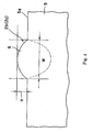
- FIGs. 1 and 2 are schematic views showing a device 4 according to an embodiment of a first aspect of the present invention.
- the main body 5 has a shape of a flat plate.
- Ground electrodes 1A, 1C and a signal electrode 1B are formed on a first main face 5a of a substrate 5.
- electrode configuration of so called Coplanar waveguide (CPW electrode) is applied.
- An optical waveguide 2 has an inlet part 2a, an outlet part 2d and a pair of branched parts 2b and 2c.
- a pair of branched parts 2b and 2c of an optical waveguide are positioned between adjacent electrodes, so that a signal voltage can be applied on the optical waveguides 2b and 2c substantially in a horizontal direction.
- the optical waveguide 2 constitutes an optical waveguide of so-called Mach-Zehnder type.
- the distance L between the branched parts 2b and 2c is preferably 46 ⁇ m or longer.
- the inventors have further reached the following discovery.
- the mode coupling of the optical waveguides is problematic in waveguide part of a Mach-Zehnder interferometer (interaction part with an electrode).
- the mode coupling between the optical waveguide parts can be reduced by forming a groove 5c between the branched optical waveguide parts as shown in Fig. 3 .
- the extinction ratio can be made 20 dB or more and the dependency of the extinction ratio on wavelength can be reduced, when the optical waveguide is made single mode propagation mode at least in a horizontal direction.
- Fig. 4 is an enlarged cross sectional view showing the optical waveguide parts 2b and 2c.
- an appropriate diffusing agent such as titanium is mounted on a main face 5a, which is then subjected to a heat treatment.
- a ridge 6 is formed on the main face 5a due to the diffusion.
- the height H of the ridge is defined as a peak height value of the swell and the width W is defined as a distance between two most distant points selected from all the points whose heights are 5 percent of the height H.
- the product of the width W and height H of the ridge 6 is made 6000 angstrom ⁇ ⁇ m according to the present invention.
- a buffer layer may be provided between the main body and electrodes. Further, the present invention may be applied in the case where the electrode configuration is of asymmetrical coplanar strip line type.
- the main body is made of a single crystal lithium niobate.
- the materials of the ground and signal electrodes are not particularly limited as far as the material is excellent in impedance characteristic, and may be composed of gold, silver, copper or the like.
- the buffer layer may be made of known materials such as silicon oxide, magnesium fluoride, silicon nitride and alumina.
- the optical waveguide is a titanium diffusion optical waveguide or proton exchange optical waveguide, and most preferably be titanium diffusion optical waveguide.
- the electrode is formed on the first main face of the main body. The electrode may be directly formed on the first main face or may be formed on the buffer layer.
- the polarization axis of the crystal is substantially parallel with the first main face 5a of the substrate, which is an X-plate lithium niobate single crystal.
- Figs. 1 to 5 show examples where the present invention is applied to an X-plate.
- the main body 5 is joined with a separate supporting body 7.
- the material of the supporting body 7 may be a material having a dielectric constant lower than that of the electro-optic material.
- Such material includes a glass such as quartz glass.
- the method of joining the optical waveguide substrate 5 and supporting body 7 is not particularly limited. According to a preferred embodiment, both are adhered.
- the refractive index of the adhesive agent may preferably be lower than that of the electro-optic material forming the main body 5.
- the adhesive agent examples include an epoxy resin type adhesive, a thermal setting resin type adhesive and an ultraviolet curable resin type adhesive.
- Such adhesive may preferably have a thermal expansion coefficient relatively close to that of a material having electro-optic effects such as lithium niobate.
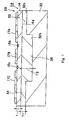
- Fig. 6 is a cross sectional view schematically showing an optical modulator 11 according mainly to the first invention.
- Fig. 6 shows the cross section substantially perpendicular to the direction of the propagation of light in a traveling wave type optical modulator.
- An optical modulator 11 has an optical waveguide substrate 29 and a supporting body 12.
- Each of the main body 14 and substrate 12 has a shape of a flat plate.
- the thickness of the main body 14 is 30 m or smaller.
- Predetermined electrodes 17A, 17B and 17C are formed on a first main face 14a of a main body 14.
- CPW electrode coplanar type electrode
- the position and shape of the electrodes are not particularly limited.
- ACPS type Asymmetric coplanar strip-line type
- a pair of optical waveguides 15b and 15c are formed between adjacent electrodes, so that a signal voltage can be applied onto the optical waveguide parts 15b and 15c, respectively, substantially in a horizontal direction.
- the optical waveguide constitutes so called Mach-Zehnder type optical waveguide in a plan view, and the planar pattern is well known (described later).
- An adhesive layer 13 having a uniform thickness is interposed between the second main face 14d of the main body 14 and the adhesive face 12a of the supporting body 12, so that the main body 14 and supporting body 12 are joined with each other.
- a flat-plate shaped main body having a thickness of 30 ⁇ m or smaller is used and adhered with a supporting body with an adhesive, and the adhesion face 12a of the supporting body is made substantially flat.
- the thickness of the adhesive layer 13 is thus made substantially constant so that the position of stress concentration can be prevented in an optical waveguide device 29.
- the stress is thus dispersed to reduce the maximum stress in the optical waveguide substrate 29.
- flat grinding can be used for processing the main body 4 to a thickness of 30 ⁇ m or smaller, so that processing damage can be considerably reduced by an appropriate means and the deterioration of the fracture strength can be prevented at the same time.
- a main body 14 is composed of a flat plate having a thickness of 30 ⁇ m.
- the flat plate herein described means a flat plate wherein a recess or groove is not formed on the main faces 14d. That is, the second face 14d (adhesion face) is substantially flat.
- the main face 14d is substantially flat, a surface roughness remaining on the surface due to the processing is permitted, and curvature and warping due to the processing are also permitted.
- optical waveguides 15b and 15c are provided on the side of the first main face 14a of the main body 14.
- the optical waveguide may be a ridge type optical waveguide directly formed on the first main face of the main body, or a ridge type optical waveguide formed on another layer on the first main face of the main body, or an optical waveguide formed by inner diffusion or ion exchange process in the inside of the main body, such as titanium diffusion or proton exchange waveguide.
- the optical waveguide may be a ridge type optical waveguide protruding from the main face 14a.
- the ridge type optical waveguide may be formed by laser or mechanical processing.
- a film of a high refractive index may be formed on the main body 14 and then processed by mechanical or laser ablation processing to produce a ridge type three-dimensional optical waveguide.
- the film of a high refractive index may be formed, for example, by chemical vapor deposition, physical vapor deposition, organic metal chemical vapor deposition, sputtering or liquid phase epitaxy process.
- the main body forming the optical waveguide substrate is composed of a single crystal.
- the polarization axis of the crystal is substantially parallel with the first main face (surface) of the substrate, which is an X-plate lithium niobate single crystal.
- Figs. 6 to 10 show examples where the present invention is applied to an X-plate.
- the minimum value of the thermal expansion coefficient of the supporting body may be 1/5 or larger of the minimum value of the thermal expansion coefficient of the main body, and the maximum value of the thermal expansion coefficient of the supporting body may be 5 times or smaller of the maximum value of the thermal expansion coefficient of the optical waveguide substrate.
- the minimum and maximum values of the thermal expansion coefficient are the same in each of the main and supporting bodies.
- the thermal expansion coefficient may be changed for the respective axes.
- the thermal expansion coefficients for X axis and Y axis are 16 x 10- 6 /°C, respectively, which is the maximum value.
- the thermal expansion coefficient in Z axis is 5 x 10 -6 /°C, which is the minimum value.
- the minimum value of the thermal expansion coefficient of the supporting body is made 1 x 10 -6 /°C or larger, and the maximum value of the thermal expansion coefficient of the supporting body is made 80 ⁇ 10 -6 /°C or smaller.
- the thermal expansion coefficient of quartz glass is 0.5 ⁇ 10 -6 /°C and thus smaller than 1 ⁇ 10 -6 /°C, for example.
- the minimum value of thermal expansion coefficient of the supporting body may more preferably be 1/2 or larger of that of the main body.
- the maximum value of thermal expansion coefficient of the supporting body may more preferably be 2 times or smaller of the maximum value of that of the main body of the optical waveguide substrate.
- the material of the supporting body is not particularly limited, as far as the above conditions are satisfied.
- the material of the supporting body includes lithium niobate, lithium tantalate, a solid solution of lithium niobate-lithium tantalate and potassium lithium niobate.
- lithium niobate same as the material of the main body is most preferred on the viewpoint of a difference of thermal expansion.
- the electrodes are provided on the first main face of the main body.
- the electrodes may be provided directly on the first main face of the main body, or provided on a low dielectric constant layer or a buffer layer.
- the low dielectric layer may be made of a known material such as silicon oxide, magnesium fluoride, silicon nitride or alumina.
- the term "low dielectric layer” means a layer composed of a material having a dielectric constant lower than that of the material forming the main body.
- the dielectric constant of the material may be preferably lower on the viewpoint of satisfying the velocity matching condition of light and micro wave.
- the thickness of the main body may preferably be 20 ⁇ m or smaller.
- the face 12a for adhesion of the supporting body 12 is substantially flat.
- the phrase "the face 12a for adhesion is substantially flat" means that surface roughness remaining after the processing and curvature and warping due to the processing are allowed.
- the thickness T1 of the adhesive layer 13 may preferably be 1000 ⁇ m or smaller, more preferably be 300 ⁇ m or smaller and most preferably be 100 ⁇ m or smaller. Further, the lower limit of the thickness T1 of the adhesive layer 13 is not particularly limited, and may be 10 ⁇ m or more on the viewpoint of reducing the effective refractive index of microwave.
- the dielectric constant of the adhesive layer is lower than that of the electro-optic material forming the main body, and the dielectric constant may preferably be 5 or lower.
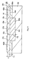
- Fig. 7 is a cross sectional view schematically showing an optical waveguide device 11A according to another embodiment of the present invention.
- Fig. 7 shows a cross section substantially perpendicular to the direction of propagation of light in a traveling type waveguide device.
- An optical modulator 11A has an optical waveguide device 29 and a supporting body 32.
- the main body 14 has a shape of a flat plate, and the thickness of the main body 14 is 30 ⁇ m or smaller.
- the constitution of the optical waveguide device 29 is same as that of the optical waveguide device 29 shown in Fig. 6 .
- a recess or groove 32b is formed on the side of the face 32a for adhesion of the main body 14 at least in the interacting part with an electrode.
- the groove 32b is elongated in the direction of light propagation (the direction perpendicular to the paper face).
- an adhesive layer 33 is interposed between the second main face 14d of the main body 14 and the face 32a for adhesion of the supporting body 32 to adhere the main body 14 and supporting body 32.
- a groove 32b is formed under the main face 14d in regions where optical waveguides 15b and 15c are formed.
- An adhesive is filled in the groove 32b to form a low dielectric portion 36.
- the flat-plate shaped main body 14 having a thickness of 30 ⁇ m or smaller is used, and the supporting body 32 and main body 14 are adhered with the adhesive layer 33.
- the thickness T1 of the adhesive layer 33 is made 200 ⁇ m or smaller. It is thus possible to facilitate the dispersion of stress in the optical waveguide substrate 29 to reduce the maximum stress applied on the optical waveguide device 29.
- the thickness T2 of the low dielectric portion 36 made of an adhesive agent is made larger than that of the thickness T1 of the adhesive layer 33, so that a step having a height of (T2-T1) is formed in the thickness of the adhesive layer.
- the thickness T1 of the adhesive layer 33 may preferably be 200 ⁇ m or smaller, for reducing the DC and temperature drifts due to such concentration of stress.
- the thickness T1 of the adhesive layer 33 is 200 ⁇ m or smaller, the thickness may preferably be 150 ⁇ m or smaller, and more preferably be 110 ⁇ m or smaller.
- the thickness T1 of the adhesive layer 33 is not particularly limited, the thickness may preferably be 0.1 ⁇ m or more on the viewpoint of reducing the stress applied on the main body 14.
- the adhesive layer may adhere the second main face and supporting body in a region where an optical waveguide is formed.
- the optical waveguide devices 11 of Fig. 6 and 11A of Fig. 7 relate to this embodiment.
- the thickness of the adhesive layer may preferably be substantially constant.
- the phrase "the thickness of the adhesive layer is substantially constant" means that an error due to production process is to be allowed.
- a low dielectric portion having a dielectric constant lower than that of the electro-optic material forming the main body between the second main face and supporting body in a region where optical waveguide is formed. It is thus possible to facilitate the velocity matching as described above.
- the low dielectric portion is not particularly limited.
- the low dielectric portion is an air layer.
- the low dielectric part is composed of an adhesive (examples of Figs. 6 and 7 ). In this case, it is needed to use an adhesive having a dielectric constant lower than that of the electro-optic material.
- the low dielectric portion is composed of a low dielectric material having a dielectric constant lower than that of the electro-optic material, and the low dielectric material does not belong to an adhesive.
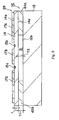
- Fig. 8 is a cross sectional view schematically showing an optical waveguide device 11B.
- the optical modulator 11B has an optical waveguide substrate 29 and a supporting body 32.
- the main body 14 has a shape of a flat plate and a thickness of 30 ⁇ m of smaller.
- a recess or groove 32b is formed on the side of the face 32a for adhesion of the main body 14 as that shown in Fig. 7 .
- the groove 32b is elongated in the direction of light propagation (direction perpendicular to the paper face).
- adhesive layers 43A and 43B are provided between the second main face 14d of the main body 14 and the adhesion face 32a of the supporting body 32 to adhere the main body 14 and supporting body 32.
- the groove 32b is formed to provide a low dielectric portion 30 under the main face 14d in regions where optical waveguides 15b and 15c are formed.
- the low dielectric portion 30 according to the present example is composed of a low dielectric material different from adhesives 43A and 43B.
- Fig. 9 is a cross sectional view schematically showing an optical waveguide device 11C.
- the optical modulator 11C has an optical waveguide substrate 29 and a supporting body 12.
- the main body 14 has a shape of a flat plate and a thickness of 30 ⁇ m of smaller.
- the adhesion face 12a of the supporting body 12 is substantially flat.
- adhesive layers 44A and 43B are provided between the second main face 14d of the main body 14 and the adhesion face 12a of the supporting body 12 to adhere the main body 14 and supporting body 12.
- An air layer 31 is formed under the main face 14d in regions where optical waveguides 15b and 15c are formed.
- the air layer 31 functions as a low dielectric portion.
- Fig. 10 is a cross sectional view schematically showing an optical waveguide device 11D.
- the optical modulator 11D has an optical waveguide substrate 29 and a supporting body 32.
- the main body 14 has a shape of a flat plate and a thickness of 30 ⁇ m of smaller.
- a recess or groove 32b is formed on the side of the face 32a for adhesion of the main body 32.
- adhesive layers 43A and 43B are provided between the second main face 14d of the main body 14 and the adhesion face 32a of the supporting body 32 to adhere the main body 14 and supporting body 32.
- the thickness T1 of each of the adhesive layers 43A and 43B is 200 ⁇ m or smaller.
- An air layer 35 is formed under the main face 14d in regions where optical waveguides 15b and 15c are formed. The air layer 35 functions as a low dielectric portion.
- the thickness T2 of the low dielectric portion 30, 35 or 36 may preferably by 10 ⁇ m or larger, and more preferably be 30 ⁇ m or larger.
- the thickness T2 of the low dielectric portion 30, 35 or 36 may preferably be 0.5 ⁇ m or smaller and more preferably be 1000 ⁇ m or smaller.
- the present invention may be also applied to a traveling wave type optical modulator of so-called independent modulation type.
- the material of the electrode is not particularly limited, as far as it has superior impedance property and a low resistance.
- the material may be gold, silver copper or the like.
- the adhesives are not particularly limited as far as the above conditions are satisfied, they include an epoxy resin type adhesive, thermal setting resin type adhesive, ultraviolet curable resin type adhesive and "Alon Ceramics C" (trade name: manufactured by Toa Gosei: thermal expansion coefficient of 13 ⁇ 10 -6 K) having a thermal expansion coefficient relatively close to that of the material having electro-optic effect such as lithium niobate.
- the adhesive glass may preferably be that having a low dielectric constant and a temperature suitable for adhesion (working temperature) of about 600 °C or lower. Further, it is preferred that a sufficient adhesive strength can be obtained after the processing. Specifically, so-called solder glass containing a composition of a plurality of ingredients such as silicon oxide, lead oxide, aluminum oxide, magnesium oxide, calcium oxide, boron oxide or the like.
- a sheet of an adhesive may be provided between the back face of the main body 14 and the supporting body to adhere them.
- a sheet made of a thermal setting, light curable or light thickening resin adhesive is provided between the back face of the main body 4 and the supporting body and cured.
- a Ti diffusion waveguide and CPW electrode pattern were formed on a lithium niobate substrate of X-cut (see Figs. 1 and 2 ).
- the gaps of the central electrode 1B and ground electrodes 1A and 1C were 25 ⁇ m , respectively, the width of the central electrode 1B was 30 ⁇ m, the thickness of each of the electrodes was 28 ⁇ m, and the length of each electrode was 32 mm.
- the distance "L" of the arms of the optical waveguide was 55 ⁇ m.
- the substrate was then subjected to polishing and thinning to produce a thin type optical modulator having a low dielectric layer and a supporting body (lithium niobate plate of X-cut).
- the thickness of the substrate 5 for optical modulator was 8.5 ⁇ m, and the low dielectric layer 6 has a dielectric constant of 3.8 and a thickness of 50 ⁇ m.
- the end face of the connecting part of an optical fiber was then subjected to polishing and the substrate was cut by dicing to produce chips.
- the modulator chips were subjected to optical axis alignment with the optical fiber and adhered and fixed with a UV curable resin.
- the height "H" and width "W" of the ridge 6 of the optical waveguide 2 measured after the production of the device was changed as shown in table 1. Further, table 1 shows the values of the products H ⁇ W. The thus obtained devices were subjected to the observation of modes. The results were shown in table 1.
- the optical waveguide was made cut-off to prevent the propagation of light therein when the width of the optical waveguide is 6 ⁇ m or smaller, under the condition that the height "H" of the swell of the optical waveguide is 1000 angstrom. It has been, however, proved that light can be propagated in single mode at a width of optical waveguide of 6 ⁇ m or smaller, for example even 3 ⁇ m or smaller, by lowering the thickness of the substrate to 30 ⁇ m or smaller. It is thus possible to prevent the deviation of operational point of applied voltage and extinction ratio depending on wavelength, by satisfying the condition that light can be propagated in single mode as described above.
- the distance "L” between optical waveguide arms was 55 ⁇ m
- the height “H” of the ridge 6 of the optical waveguide 2 was 860 angstrom
- the width "W” was 6 ⁇ m
- the product of both was made 5160 angstrom ⁇ ⁇ m.
- S21 of the device was measured to prove that no ripple was found in a wavelength range of 50 GHz or lower, the curve of the graph was smooth and was lowered by minus 6 dB only in a range of 30 GHz or higher. Further, S11 was minus 10 dB or larger in a measured range of up to 50 GHz. Further, the mode was observed as an optical property. The observed mode proved to be single mode, the extinction ratio was 20 dB or more in a range of 1530 nm to 1610 nm, and the dependency of extinction ratio curve on voltage was proved to be small and ⁇ 5 percent or smaller.
- Fig. 12 shows the relationship of the extinction ratio and applied voltage according to the present example.
- the heights of the peaks are substantially constant, and the positions of the peaks and bottoms are substantially constant.
- ⁇ P optical strength of ON light
- the gap between the central electrode 1B and ground electrode 1A or 1C was made 40 ⁇ m
- the width of the central electrode 1B was 30 ⁇ m
- the thickness of each electrode was 28 ⁇ m
- the length of the electrode was 40 ⁇ m.
- the distance “L” between optical waveguide arms was made 70 ⁇ m
- the height "H” of the ridge 6 of the optical waveguide 2 was 860 angstrom
- the width "W” was 6 ⁇ m
- the product of both was made 5160 angstrom ⁇ ⁇ m.
- S21 of the device was measured to prove that no ripple was found in a wavelength range of 50 GHz or lower, the curve of the graph was smooth and was lowered by minus 6 dB only in a range of 25 GHz or higher. Further, S11 was minus 10 dB or smaller in a measured range of up to 50 GHz. Further, the mode was observed as an optical property. The observed mode proved to be single mode, the extinction ratio was 20 dB or more in a range of 1530 nm to 1610 nm, and the dependency of extinction ratio curve on voltage was proved to be small and ⁇ 5 percent or smaller.
- a thin type modulator was produced according to the same procedure as the Example 2.
- the distance between optical waveguide arms was 55 ⁇ m
- the width "W” was 6 ⁇ m
- the height "H” of the ridge 6 of the optical waveguide 2 was 1150 angstrom
- the product of both was made 6900 angstrom - ⁇ m.
- S21 of the device was measured to prove that no ripple was found in a wavelength range of 50 GHz or lower, the curve of the graph was smooth and was lowered by minus 6 dB only in a range of 30 GHZ or higher. Further, S11 was minus 10 dB or smaller in a measured range of up to 50 GHz. Further, the mode was observed as an optical property. The observed mode proved to be single mode, the extinction ratio was 20 dB or more in a range of 1530 nm to 1610 nm, and the dependency of extinction ratio curve on voltage was proved to be small and ⁇ 5 percent or smaller.
- a thin type modulator was produced according to the same procedure as the Example 2.
- the width of the central electrode was made 20 ⁇ m and the distance between optical waveguide arms was made as small as 45 ⁇ m.
- the width "W” was 6 ⁇ m
- the height "H” of the ridge 6 of the optical waveguide 2 was 860 angstrom and the product of both was made 6900 angstrom ⁇ ⁇ m.
- S21 of the device was measured to prove that no ripple was found in a wavelength range of 50 GHz or lower, the curve of the graph was smooth and was lowered by minus 6 dB only in a range of 30 GHz or higher. Further, S11 was minus 10 dB or lower in a measured range of up to 50 GHz. Further, the mode was observed as an optical property.
- the observed mode proved to be single mode, the extinction ratio was lower than 20 dB in a part of a range of 1530 nm to 1610 nm, and the dependency of extinction ratio curve on voltage was proved to be small and ⁇ 5 percent or smaller.
- a thin type modulator was produced according to the same procedure as the Example 2.
- the width of the central electrode was made 20 ⁇ m and the distance between optical waveguide arms was as small as 45 ⁇ m, as the Example 5.
- the width "W” was 6 ⁇ m
- the height "H” of the ridge 6 of the optical waveguide 2 was 860 angstrom and the product of both was made 6900 angstrom ⁇ ⁇ m.
- the groove was formed by means of excimer laser processing.
- S21 of the device was measured to prove that no ripple was found in a wavelength range of 50 GHz or lower, the curve of the graph was smooth and was lowered by minus 6 dB only in a range of 30 GHz or higher. Further, S11 was minus 10 dB in a measured range of up to 50 GHz. Further, the mode was observed as an optical property. The observed mode proved to be single mode, the extinction ratio was 20 dB or more in a range of 1530 nm to 1610 nm, and the dependency of extinction ratio curve on voltage was proved to be small and ⁇ 5 percent or smaller.
- a thin type modulator was produced according to the same procedure as the Example 2.
- the distance between optical waveguide arms was 55 ⁇ m.
- the width "W" of the ridge 6 of the optical waveguide 2 was 6.5 ⁇ m, the height “H” was 1150 angstrom, and the product of both was made 7475 angstrom ⁇ ⁇ m.
- S21 of the device was measured to prove that no ripple was found in a wavelength range of 50 GHz or lower, the curve of the graph was smooth and was lowered by minus 6 dB only in a range of 30 GHz or higher. Further, S11 was minus 10 dB in a measured range of up to 50 GHz.
- the mode was observed as an optical property.
- the observed mode proved to be multi mode.
- the extinction ratio was lower than 20 dB in a part of a range of 1530 nm to 1610 nm, and the dependency of extinction ratio curve on voltage was proved to be larger than ⁇ 5 percent.
- Fig. 11 shows the relationship of the extinction ratio and applied voltage according to the present example.
- the heights of the peaks are deviated, and the positions of the peaks and bottoms are not constant.
- a device was produced according to the same procedure as the Example 2.
- the height of the recess was 860 angstrom, the width was 5 ⁇ m and the product of both was made 4300 angstrom ⁇ ⁇ m.
- the distance of the optical waveguide arms (distance "L" of the branched parts 2b and 2c) was changed as shown in Figs. 16 and 17 .
- the dependency of the extinction ratio with respect to "L” was shown in Fig. 16
- the dependency of ⁇ P with respect to "L” was shown in Fig. 17 .
- the extinction ratio can be made 20 dB or more over a wide range of wavelength and ⁇ P can be controlled within ⁇ 5 % by increasing the distance "L" of arms to 46 ⁇ m or more.
- "L" may more preferably be 50 ⁇ m or more.
- a device was produced according to the same procedure as the Example 2.
- the height of the recess was 1150 angstrom, the width was 5 ⁇ m and the product of both was made 5750 angstrom ⁇ ⁇ m.
- the distance of the optical waveguide arms (distance "L" of the branched parts 2b and 2c) was changed as shown in Figs. 18 and 19 .
- the dependency of the extinction ratio with respect to "L” was shown in Fig. 18
- the dependency of ⁇ P with respect to "L” was shown in Fig. 19 .
- the extinction ratio can be made 20 dB or more over a wide range of wavelength by increasing the distance "L" of arms to 46 ⁇ m or more. Further, according to the present example, ⁇ P cannot be made within ⁇ 5%.
- An optical modulator 11 of Fig. 6 was produced. Specifically, a substrate made of 3 inch wafer (LiNbO 3 single crystal) of X-cut was used. Mach-Zehnder type optical waveguides 15b, 15c are formed on the surface of the wafer by titanium diffusion and photolithography. The size of the optical waveguide can be made 10 ⁇ m at 1/e 2 , for example. A CPW electrode pattern is then formed by plating process. The gaps between the central electrode 17B and ground electrodes 17A, 17C are made 40 ⁇ m, respectively, the thickness of the electrode is made 28 ⁇ m and the length of the electrode is made 40 mm.
- a dummy wafer for polishing is adhered with a thermoplastic resin onto a surface plate for polishing, and the modulator substrate is adhered onto the dummy wafer by a thermoplastic resin with the electrode side downwardly. Further, the main body 14 is processed to a thickness of 10 ⁇ m by lateral grinding and polishing (CMP). Thereafter, a flat plate-shaped supporting body 12 is adhered and fixed to the main body 14, the end face of the connecting part for an optical fiber is polished, and cut by dicing to chips.
- the resin for adhesion and fixing was an epoxy resin film having a resin thickness of 50 ⁇ m.
- the width of the chip was 4.4 mm and the total thickness of the chip and reinforcing supporting body was made 1 mm.
- a single core fiber array holding 1.55 ⁇ m band Panda fibers is connected to the input side and a single core fiber array holding single mode optical fibers is connected to the output side of the traveling wave type optical modulator.
- the optical fibers and optical waveguide is optically aligned and the fiber arrays and modulator are adhered with a thermosetting resin adhesive.
- the substrate of X-cut 3 inch wafer (LiNbO 3 single crystal) was used.
- the thermal expansion coefficients in the X-axis and Y-axis are 16 ⁇ 10 -6 /°C, respectively, and the thermal expansion coefficients in the Z-axis is 5 ⁇ 10 -6 /°C.
- the material of the supporting body 2 was x-cut lithium niobate single crystal.
- Fig. 20 The extinction curve with respect to a signal of 1KHz is shown in Fig. 20 . As can be seen from the results, no hysteresis was observed in the optical power. Further, the DC drift was evaluated at 100 °C to prove that the shift amount of the DC bias was within a deviation of 50 percent with respect to the initial applied voltage.
- the device 11C of Fig. 9 was produced. Specifically, an optical waveguide 29 was produced according to the same procedure as the Example 9. The thickness "t" of the main body 14 was made 12 ⁇ m. An air layer 31 was provided as shown in Fig. 9 . According to the present example, the main body of X-cut LiNbO 3 single crystal was used. The material of the supporting body 12 was x-cut lithium niobate single crystal.
- Hysteresis was not observed in the extinction curve with respect to a signal of 1KHz. Further, the DC drift was evaluated at 100 °C to prove that the shift amount of the DC bias was within a deviation of 50 percent with respect to the initial applied voltage.
- the device 11A of Fig. 7 was produced. Specifically, an optical waveguide substrate 29 was produced according to the same procedure as the Example 9. Thereafter, a supporting body 32 with a groove 32b having a width of 0.3 mm and a depth of 0.2 mm formed was adhered to the optical waveguide substrate 29. the end face of the connecting part for an optical fiber was polished and cut by dicing to chips. Adhesive resin 36 was filled in the groove 32b of the supporting body 32. T1 was thus 50 ⁇ m and T2 was 250 ⁇ m. According to the present example, a main body of X-cut single crystal of LiNb03 was used. The material of the supporting body 12 was X-cut lithium niobate single crystal.
- Hysterisis was not observed in the extinction curve with respect to a signal of 1KHz. Further, the DC drift was evaluated at 100 °C to prove that the shift amount of the DC bias was within a deviation of 50 percent with respect to the initial applied voltage.
- the device 11D of Fig. 10 was produced. Specifically, an optical waveguide 29 was produced according to the same procedure as the Example 1. The thickness of the main body 14 was made 12 ⁇ m. Thereafter, a supporting body 32 with a groove 32b having a width of 0.3 mm and a depth of 0.2 mm formed was adhered to the optical waveguide substrate 29. The end face of the connecting part for an optical fiber was polished and cut by dicing to chips. An air layer 35 was formed in the groove 32b of the supporting body 32. T1 was thus 50 ⁇ m and T2 was 250 ⁇ m. According to the present example, a main body of X-cut single crystal of LiNbO3 was used. The material of the supporting body 12 was X-cut lithium niobate single crystal.
- Hysteresis was not observed in the extinction curve with respect to a signal of 1KHz. Further, the DC drift was evaluated at 100 °C to prove that the shift amount of the DC bias was within a deviation of 50 percent with respect to the initial applied voltage.
- the material of the supporting body 12 was changed to lithium tantalate.
- a substrate made of 3 inch wafer of x-cut (LiNbO 3 single crystal).
- the thermal expansion coefficients in the X-axis and Y-axis are 16 ⁇ 10 -6 /°C, respectively, and the thermal expansion coefficient in the Z-axis is 5 ⁇ 10 -6 /°C.
- the material of the supporting body 2 was X-cut lithium tantalate single crystal whose thermal expansion coefficients in the X-axis and Y-axis are 16 ⁇ 10 -6 /°C, respectively, and the thermal expansion coefficient in the Z-axis is 1.2 ⁇ 10 -6 /°C.
- a substrate made of 3 inch wafer of x-cut (LiNbO 3 single crystal) was used.
- the thermal expansion coefficients in the X-axis and Y-axis are 16 ⁇ 10 -6 /°C, respectively, and the thermal expansion coefficient in the Z-axis is 5 ⁇ 10 6 /°C.
- the material of the supporting body 2 was quartz glass whose thermal expansion coefficient is 50 ⁇ 10 -6 /°C.
Claims (7)
- Dispositif de guide d'ondes optique comprenant :un substrat (5) de monocristal taille X de niobate de lithium ;des électrodes de signal (1B) et de masse (1A, 1C) pour la modulation formées sur une première face principale (5a) du substrat (5) ; etun guide d'ondes optique formé par diffusion de titane (2) prévu entre lesdites électrodes de signal (1B) et de masse (1A, 1C) et comprenant une partie d'entrée (2a), une partie de sortie (2d), et une paire de parties ramifiées (2b, 2c), dans lequel dans une région pour l'application d'un champ électrique, la paire de parties ramifiées (2b, 2c) est positionnée entre des électrodes adjacentes de sorte qu'une tension de signal puisse être appliquée sur les parties ramifiées (2b, 2c) ;dans lequel ledit substrat (5) a une épaisseur inférieure ou égale à 30 µm au moins dans la région où les électrodes de signal (1B) et de masse (1A, 1C) peuvent appliquer un champ électrique, etdans lequel le dispositif de guide d'ondes optique comprend en outre un corps de support (7) pour supporter ledit substrat (5) et une couche adhésive pour faire adhérer ledit substrat (5) et ledit corps de support (7) ;caractérisé en ce quele guide d'ondes optique (2) est configuré pour une propagation en mode simple dans la bande de 1,55 µm, et chacune des parties ramifiées (2b, 2c) dudit guide d'ondes optique (2) comprend une bosse (6) par rapport à la face principale (5a) dudit substrat (5), ladite bosse (6) lorsqu'elle est vue en coupe transversale prise perpendiculairement à la direction d'extension des parties ramifiées (2b, 2c) ayant une hauteur H (angstrom) définie en tant que valeur de hauteur de pic et une largeur W (pm) définie en tant que distance entre les deux points les plus éloignés choisis parmi tous les points dont les hauteurs représentent 5 pour cent de la hauteur H dont le produit (H x W) est inférieur ou égal à 6000 Ångströms.µm et supérieur ou égal à 3000 Ângstroms.pm.
- Substrat de guide d'ondes optique de la revendication 1, dans lequel lesdites parties ramifiées (2b, 2c) sont éloignées l'une de l'autre de 46 µm ou plus.
- Dispositif de guide d'ondes optique de la revendication 1, dans lequel une rainure (5c) est formée dans ledit substrat (5) entre lesdites parties ramifiées (2b, 2c).
- Dispositif de guide d'ondes optique de l'une quelconque des revendications 1 à 3, dans lequel la valeur minimale d'un coefficient de dilatation thermique linéaire dudit corps de support (7) est supérieure ou égale à 1/5 de la valeur minimale d'un coefficient de dilatation thermique linéaire dudit substrat (5), et dans lequel la valeur maximale d'un coefficient de dilatation thermique linéaire dudit corps de support (7) est 5 fois ou moins la valeur maximale d'un coefficient de dilatation thermique linéaire dudit substrat (5).
- Dispositif de guide d'ondes optique de la revendication 4, dans lequel ledit corps de support (7) comprend un ou plusieurs matériau(x) choisi(s) dans le groupe constitué de niobate de lithium, de tantalate de lithium, d'une solution solide de niobate de lithium-tantalate de lithium et de niobate de lithium et de potassium.
- Dispositif de guide d'ondes optique de l'une quelconque des revendications 1 à 5, dans lequel ledit corps de support (7) comprend un monocristal de niobate de lithium.
- Dispositif de guide d'ondes optique de l'une quelconque des revendications 1 à 6, dans lequel ladite bosse a une hauteur H inférieure ou égale à 1100 Ângstroms et une largeur "W" inférieure ou égale à 6,5 pm.
Priority Applications (1)
| Application Number | Priority Date | Filing Date | Title |
|---|---|---|---|
| EP10169806A EP2237105A3 (fr) | 2003-08-21 | 2004-08-19 | Dispositifs de guide d'ondes optiques et modulateurs optiques de type onde progressive |
Applications Claiming Priority (3)
| Application Number | Priority Date | Filing Date | Title |
|---|---|---|---|
| JP2003297527 | 2003-08-21 | ||
| US88645704A | 2004-07-07 | 2004-07-07 | |
| PCT/JP2004/012221 WO2005019913A1 (fr) | 2003-08-21 | 2004-08-19 | Dispositif de guide d'ondes optique et modulateur optique de type a onde itinerante |
Related Child Applications (1)
| Application Number | Title | Priority Date | Filing Date |
|---|---|---|---|
| EP10169806A Division-Into EP2237105A3 (fr) | 2003-08-21 | 2004-08-19 | Dispositifs de guide d'ondes optiques et modulateurs optiques de type onde progressive |
Publications (3)
| Publication Number | Publication Date |
|---|---|
| EP1657588A1 EP1657588A1 (fr) | 2006-05-17 |
| EP1657588A4 EP1657588A4 (fr) | 2007-11-14 |
| EP1657588B1 true EP1657588B1 (fr) | 2015-03-04 |
Family
ID=34220705
Family Applications (2)
| Application Number | Title | Priority Date | Filing Date |
|---|---|---|---|
| EP04772177.4A Active EP1657588B1 (fr) | 2003-08-21 | 2004-08-19 | Dispositif de guide d'ondes optique et modulateur optique de type a onde itinerante |
| EP10169806A Withdrawn EP2237105A3 (fr) | 2003-08-21 | 2004-08-19 | Dispositifs de guide d'ondes optiques et modulateurs optiques de type onde progressive |
Family Applications After (1)
| Application Number | Title | Priority Date | Filing Date |
|---|---|---|---|
| EP10169806A Withdrawn EP2237105A3 (fr) | 2003-08-21 | 2004-08-19 | Dispositifs de guide d'ondes optiques et modulateurs optiques de type onde progressive |
Country Status (4)
| Country | Link |
|---|---|
| US (1) | US7502530B2 (fr) |
| EP (2) | EP1657588B1 (fr) |
| JP (1) | JP5063001B2 (fr) |
| WO (1) | WO2005019913A1 (fr) |
Cited By (1)
| Publication number | Priority date | Publication date | Assignee | Title |
|---|---|---|---|---|
| RU2678205C1 (ru) * | 2015-01-07 | 2019-01-24 | Файберхоум Телекоммьюникейшн Текнолоджиз Ко., Лтд | Сохраняющее состояние поляризации оптическое волокно малого диаметра |
Families Citing this family (32)
| Publication number | Priority date | Publication date | Assignee | Title |
|---|---|---|---|---|
| EP1657588B1 (fr) * | 2003-08-21 | 2015-03-04 | NGK Insulators, Ltd. | Dispositif de guide d'ondes optique et modulateur optique de type a onde itinerante |
| JP4868763B2 (ja) * | 2005-03-31 | 2012-02-01 | 住友大阪セメント株式会社 | 光変調器 |
| JP2007114222A (ja) * | 2005-03-31 | 2007-05-10 | Sumitomo Osaka Cement Co Ltd | 光制御素子 |
| JP2007101641A (ja) * | 2005-09-30 | 2007-04-19 | Sumitomo Osaka Cement Co Ltd | 光変調器及びその製造方法 |
| JP2007264522A (ja) * | 2006-03-30 | 2007-10-11 | Sumitomo Osaka Cement Co Ltd | 光導波路デバイス、光導波路モジュール、および光導波路デバイスの製造方法 |
| JP2009086336A (ja) * | 2007-09-28 | 2009-04-23 | Sumitomo Osaka Cement Co Ltd | 光導波路型デバイス |
| JP2009181108A (ja) * | 2008-02-01 | 2009-08-13 | Sumitomo Osaka Cement Co Ltd | 光導波路素子 |
| JP4961372B2 (ja) * | 2008-02-29 | 2012-06-27 | 住友大阪セメント株式会社 | 光導波路デバイス |
| JP5386841B2 (ja) * | 2008-03-24 | 2014-01-15 | 住友大阪セメント株式会社 | 光変調器 |
| JP2010085789A (ja) * | 2008-09-30 | 2010-04-15 | Sumitomo Osaka Cement Co Ltd | 光導波路素子 |
| JP4954958B2 (ja) * | 2008-09-30 | 2012-06-20 | 住友大阪セメント株式会社 | 光導波路素子 |
| WO2010082673A1 (fr) * | 2009-01-16 | 2010-07-22 | 日本碍子株式会社 | Guide d'ondes optique ramifié, substrat de guide d'ondes optique et modulateur optique |
| JP4782213B2 (ja) * | 2009-03-19 | 2011-09-28 | 住友大阪セメント株式会社 | 光導波路デバイス |
| JP5313198B2 (ja) * | 2010-03-30 | 2013-10-09 | 住友大阪セメント株式会社 | 導波路型偏光子 |
| JP2012073328A (ja) * | 2010-09-28 | 2012-04-12 | Sumitomo Osaka Cement Co Ltd | 光変調器 |
| JP5691808B2 (ja) * | 2011-04-28 | 2015-04-01 | 住友大阪セメント株式会社 | 光導波路デバイス |
| US8644650B2 (en) * | 2011-12-30 | 2014-02-04 | Infinera Corporation | Mach-Zehnder having segmented drive signal electrodes |
| JP5720737B2 (ja) * | 2013-07-23 | 2015-05-20 | 住友大阪セメント株式会社 | 光導波路素子 |
| CN107966832A (zh) * | 2016-10-18 | 2018-04-27 | 天津领芯科技发展有限公司 | 一种低直流漂移的铌酸锂薄膜强度调制器 |
| US10295849B2 (en) * | 2016-12-16 | 2019-05-21 | Lumentum Operations Llc | Optical modulator |
| JP7037199B2 (ja) * | 2017-03-23 | 2022-03-16 | 兵庫県公立大学法人 | 光変調器 |
| JP7115483B2 (ja) * | 2017-08-24 | 2022-08-09 | Tdk株式会社 | 光変調器 |
| JPWO2019117313A1 (ja) * | 2017-12-15 | 2020-12-17 | 古河電気工業株式会社 | 光偏波素子およびその製造方法 |
| JP6992625B2 (ja) | 2018-03-16 | 2022-01-13 | 三菱ケミカル株式会社 | コークス製造用粘結材の製造方法 |
| JP7052477B2 (ja) * | 2018-03-28 | 2022-04-12 | 住友大阪セメント株式会社 | 光導波路素子 |
| JP7069966B2 (ja) * | 2018-03-29 | 2022-05-18 | 住友大阪セメント株式会社 | 光制御素子 |
| JP7118844B2 (ja) * | 2018-10-03 | 2022-08-16 | 株式会社日本製鋼所 | 光変調器、光変調器用基板、光変調器の製造方法及び光変調器用基板の製造方法 |
| WO2020095421A1 (fr) * | 2018-11-08 | 2020-05-14 | 日本碍子株式会社 | Substrat composite pour dispositif électro-optique et procédé de fabrication associé |
| JP7334616B2 (ja) * | 2019-12-26 | 2023-08-29 | 住友大阪セメント株式会社 | 光導波路素子、光変調器、光変調モジュール、及び光送信装置 |
| JP7380204B2 (ja) * | 2019-12-26 | 2023-11-15 | 住友大阪セメント株式会社 | 光導波路デバイス |
| WO2021247565A1 (fr) * | 2020-06-02 | 2021-12-09 | HyperLight Corporation | Modulateurs optiques et circuits d'attaque à hautes performances |
| US11940713B2 (en) * | 2020-11-10 | 2024-03-26 | International Business Machines Corporation | Active electro-optic quantum transducers comprising resonators with switchable nonlinearities |
Family Cites Families (28)
| Publication number | Priority date | Publication date | Assignee | Title |
|---|---|---|---|---|
| JPS56164313A (en) | 1980-05-22 | 1981-12-17 | Nippon Telegr & Teleph Corp <Ntt> | Waveguide type light modulator |
| JPH04163420A (ja) | 1990-10-26 | 1992-06-09 | Fujitsu Ltd | 光変調器の実装方法 |
| JPH04371913A (ja) | 1991-06-20 | 1992-12-24 | Matsushita Electric Ind Co Ltd | 光変調器および光スイッチ |
| JP2919132B2 (ja) | 1991-09-27 | 1999-07-12 | 日本電気株式会社 | 光変調器 |
| JPH05264937A (ja) | 1992-03-23 | 1993-10-15 | Nippon Telegr & Teleph Corp <Ntt> | 光制御デバイス |
| KR0134763B1 (ko) | 1992-04-21 | 1998-04-23 | 다니이 아끼오 | 광도파로소자와 그 제조방법 |
| JP2581486B2 (ja) | 1992-04-27 | 1997-02-12 | 松下電器産業株式会社 | 光導波路素子およびその製造方法 |
| JPH06281829A (ja) | 1993-03-25 | 1994-10-07 | Ibiden Co Ltd | シングルモード光導波路 |
| JPH07281140A (ja) * | 1993-10-14 | 1995-10-27 | Sony Corp | 電気光学変調器 |
| JPH09211402A (ja) | 1996-01-30 | 1997-08-15 | Matsushita Electric Ind Co Ltd | 広帯域光変調素子 |
| JP3603977B2 (ja) | 1996-09-06 | 2004-12-22 | 日本碍子株式会社 | 進行波形光変調器およびその製造方法 |
| US5991489A (en) | 1996-12-27 | 1999-11-23 | Ngk Insulators, Ltd. | Optical Ti-diffused LiNbO3 waveguide device and method of manufacturing same |
| JP3875385B2 (ja) | 1996-12-27 | 2007-01-31 | 日本碍子株式会社 | 光導波路素子及び光導波路素子の製造方法 |
| US6567598B1 (en) | 1998-05-11 | 2003-05-20 | California Institute Of Technology | Titanium-indiffusion waveguides |
| JP2001101729A (ja) | 1999-09-27 | 2001-04-13 | Sanyo Electric Co Ltd | 光ディスク記録再生装置 |
| JP4408558B2 (ja) | 1999-12-15 | 2010-02-03 | 日本碍子株式会社 | 進行波形光変調器およびその製造方法 |
| EP1109054B1 (fr) | 1999-12-15 | 2005-08-17 | Ngk Insulators, Ltd. | Modulateur optique à ondes progressives et son procédé de fabrication |
| JP4471520B2 (ja) | 2000-09-22 | 2010-06-02 | 日本碍子株式会社 | 進行波形光変調器 |
| DE60107360T2 (de) | 2000-09-22 | 2005-11-03 | Ngk Insulators, Ltd. | Optischer Wanderwellenmodulator |
| JP2002357797A (ja) | 2001-03-30 | 2002-12-13 | Ngk Insulators Ltd | 光導波路デバイス、その製造方法および進行波形光変調器 |
| JP2002330325A (ja) | 2001-05-02 | 2002-11-15 | Seiko Epson Corp | デジタルカメラ |
| US6760493B2 (en) * | 2001-06-28 | 2004-07-06 | Avanex Corporation | Coplanar integrated optical waveguide electro-optical modulator |
| JP3963313B2 (ja) | 2001-09-05 | 2007-08-22 | 日本碍子株式会社 | 光導波路デバイス、光変調器および光変調器の実装構造 |
| JP4375597B2 (ja) * | 2001-11-16 | 2009-12-02 | 日本碍子株式会社 | 光導波路デバイスおよび進行波形光変調器 |
| JP2004070136A (ja) * | 2002-08-08 | 2004-03-04 | Ngk Insulators Ltd | 光導波路デバイスおよび進行波形光変調器 |
| JP2004170931A (ja) * | 2002-11-05 | 2004-06-17 | Ngk Insulators Ltd | 光変調器 |
| JP4453894B2 (ja) | 2003-05-15 | 2010-04-21 | 日本碍子株式会社 | 光導波路デバイスおよび進行波形光変調器 |
| EP1657588B1 (fr) * | 2003-08-21 | 2015-03-04 | NGK Insulators, Ltd. | Dispositif de guide d'ondes optique et modulateur optique de type a onde itinerante |
-
2004
- 2004-08-19 EP EP04772177.4A patent/EP1657588B1/fr active Active
- 2004-08-19 EP EP10169806A patent/EP2237105A3/fr not_active Withdrawn
- 2004-08-19 WO PCT/JP2004/012221 patent/WO2005019913A1/fr active Application Filing
- 2004-08-19 JP JP2005513356A patent/JP5063001B2/ja active Active
- 2004-08-19 US US10/568,888 patent/US7502530B2/en active Active
Cited By (1)
| Publication number | Priority date | Publication date | Assignee | Title |
|---|---|---|---|---|
| RU2678205C1 (ru) * | 2015-01-07 | 2019-01-24 | Файберхоум Телекоммьюникейшн Текнолоджиз Ко., Лтд | Сохраняющее состояние поляризации оптическое волокно малого диаметра |
Also Published As
| Publication number | Publication date |
|---|---|
| US20070147722A1 (en) | 2007-06-28 |
| EP1657588A4 (fr) | 2007-11-14 |
| EP2237105A3 (fr) | 2011-01-26 |
| EP1657588A1 (fr) | 2006-05-17 |
| JP5063001B2 (ja) | 2012-10-31 |
| EP2237105A2 (fr) | 2010-10-06 |
| WO2005019913A1 (fr) | 2005-03-03 |
| US7502530B2 (en) | 2009-03-10 |
| JPWO2005019913A1 (ja) | 2006-10-19 |
Similar Documents
| Publication | Publication Date | Title |
|---|---|---|
| EP1657588B1 (fr) | Dispositif de guide d'ondes optique et modulateur optique de type a onde itinerante | |
| US7035485B2 (en) | Optical waveguide device, and a travelling wave form optical modulator | |
| EP1795946B1 (fr) | Dispositif à fonctionnement optique | |
| EP1722266B1 (fr) | Modulateur optique à ondes progressives | |
| US20070104407A1 (en) | Optical waveguide devices | |
| US7068863B2 (en) | Optical waveguide device, an optical modulator, a mounting structure for an optical waveguide device and a supporting member for an optical waveguide substrate | |
| US7319800B2 (en) | Optical waveguide device | |
| EP2485081A1 (fr) | Elément de guide d'ondes optiques | |
| US7529447B2 (en) | Optical waveguide devices | |
| WO2009096237A1 (fr) | Dispositif de guide d'ondes optique | |
| US6950580B2 (en) | Optical waveguide devices and travelling wave type optical modulators | |
| CN100447615C (zh) | 光波导器件以及行波型光学调制器 | |
| US7974501B2 (en) | Optical modulators | |
| US7218819B2 (en) | Electrode systems for optical modulation and optical modulators | |
| JP4453894B2 (ja) | 光導波路デバイスおよび進行波形光変調器 | |
| EP1193536B1 (fr) | Modulateur optique à onde progressive |
Legal Events
| Date | Code | Title | Description |
|---|---|---|---|
| PUAI | Public reference made under article 153(3) epc to a published international application that has entered the european phase |
Free format text: ORIGINAL CODE: 0009012 |
|
| AK | Designated contracting states |
Kind code of ref document: A1 Designated state(s): DE FR GB |
|
| 17P | Request for examination filed |
Effective date: 20060309 |
|
| DAX | Request for extension of the european patent (deleted) | ||
| RBV | Designated contracting states (corrected) |
Designated state(s): DE FR GB |
|
| A4 | Supplementary search report drawn up and despatched |
Effective date: 20071017 |
|
| 17Q | First examination report despatched |
Effective date: 20080904 |
|
| GRAP | Despatch of communication of intention to grant a patent |
Free format text: ORIGINAL CODE: EPIDOSNIGR1 |
|
| INTG | Intention to grant announced |
Effective date: 20140916 |
|
| GRAS | Grant fee paid |
Free format text: ORIGINAL CODE: EPIDOSNIGR3 |
|
| GRAA | (expected) grant |
Free format text: ORIGINAL CODE: 0009210 |
|
| AK | Designated contracting states |
Kind code of ref document: B1 Designated state(s): DE FR GB |
|
| REG | Reference to a national code |
Ref country code: GB Ref legal event code: FG4D |
|
| REG | Reference to a national code |
Ref country code: DE Ref legal event code: R096 Ref document number: 602004046739 Country of ref document: DE Effective date: 20150416 |
|
| REG | Reference to a national code |
Ref country code: DE Ref legal event code: R097 Ref document number: 602004046739 Country of ref document: DE |
|
| PLBE | No opposition filed within time limit |
Free format text: ORIGINAL CODE: 0009261 |
|
| STAA | Information on the status of an ep patent application or granted ep patent |
Free format text: STATUS: NO OPPOSITION FILED WITHIN TIME LIMIT |
|
| 26N | No opposition filed |
Effective date: 20151207 |
|
| REG | Reference to a national code |
Ref country code: FR Ref legal event code: PLFP Year of fee payment: 13 |
|
| REG | Reference to a national code |
Ref country code: FR Ref legal event code: PLFP Year of fee payment: 14 |
|
| REG | Reference to a national code |
Ref country code: FR Ref legal event code: PLFP Year of fee payment: 15 |
|
| PGFP | Annual fee paid to national office [announced via postgrant information from national office to epo] |
Ref country code: FR Payment date: 20180813 Year of fee payment: 7 |
|
| PG25 | Lapsed in a contracting state [announced via postgrant information from national office to epo] |
Ref country code: FR Free format text: LAPSE BECAUSE OF NON-PAYMENT OF DUE FEES Effective date: 20190831 |
|
| PGFP | Annual fee paid to national office [announced via postgrant information from national office to epo] |
Ref country code: GB Payment date: 20220630 Year of fee payment: 19 |
|
| PGFP | Annual fee paid to national office [announced via postgrant information from national office to epo] |
Ref country code: DE Payment date: 20220621 Year of fee payment: 19 |
|
| REG | Reference to a national code |
Ref country code: DE Ref legal event code: R119 Ref document number: 602004046739 Country of ref document: DE |