EP1638136A1 - Plaquette epitaxiale en silicium et son procede de fabrication - Google Patents
Plaquette epitaxiale en silicium et son procede de fabrication Download PDFInfo
- Publication number
- EP1638136A1 EP1638136A1 EP04745765A EP04745765A EP1638136A1 EP 1638136 A1 EP1638136 A1 EP 1638136A1 EP 04745765 A EP04745765 A EP 04745765A EP 04745765 A EP04745765 A EP 04745765A EP 1638136 A1 EP1638136 A1 EP 1638136A1
- Authority
- EP
- European Patent Office
- Prior art keywords
- plane
- trench
- normal line
- source gas
- silicon
- Prior art date
- Legal status (The legal status is an assumption and is not a legal conclusion. Google has not performed a legal analysis and makes no representation as to the accuracy of the status listed.)
- Ceased
Links
Images


Classifications
-
- H—ELECTRICITY
- H10—SEMICONDUCTOR DEVICES; ELECTRIC SOLID-STATE DEVICES NOT OTHERWISE PROVIDED FOR
- H10D—INORGANIC ELECTRIC SEMICONDUCTOR DEVICES
- H10D30/00—Field-effect transistors [FET]
- H10D30/01—Manufacture or treatment
- H10D30/021—Manufacture or treatment of FETs having insulated gates [IGFET]
- H10D30/028—Manufacture or treatment of FETs having insulated gates [IGFET] of double-diffused metal oxide semiconductor [DMOS] FETs
- H10D30/0291—Manufacture or treatment of FETs having insulated gates [IGFET] of double-diffused metal oxide semiconductor [DMOS] FETs of vertical DMOS [VDMOS] FETs
-
- H—ELECTRICITY
- H10—SEMICONDUCTOR DEVICES; ELECTRIC SOLID-STATE DEVICES NOT OTHERWISE PROVIDED FOR
- H10D—INORGANIC ELECTRIC SEMICONDUCTOR DEVICES
- H10D62/00—Semiconductor bodies, or regions thereof, of devices having potential barriers
- H10D62/01—Manufacture or treatment
- H10D62/051—Forming charge compensation regions, e.g. superjunctions
-
- H—ELECTRICITY
- H10—SEMICONDUCTOR DEVICES; ELECTRIC SOLID-STATE DEVICES NOT OTHERWISE PROVIDED FOR
- H10D—INORGANIC ELECTRIC SEMICONDUCTOR DEVICES
- H10D62/00—Semiconductor bodies, or regions thereof, of devices having potential barriers
- H10D62/10—Shapes, relative sizes or dispositions of the regions of the semiconductor bodies; Shapes of the semiconductor bodies
- H10D62/102—Constructional design considerations for preventing surface leakage or controlling electric field concentration
- H10D62/103—Constructional design considerations for preventing surface leakage or controlling electric field concentration for increasing or controlling the breakdown voltage of reverse-biased devices
- H10D62/105—Constructional design considerations for preventing surface leakage or controlling electric field concentration for increasing or controlling the breakdown voltage of reverse-biased devices by having particular doping profiles, shapes or arrangements of PN junctions; by having supplementary regions, e.g. junction termination extension [JTE]
- H10D62/109—Reduced surface field [RESURF] PN junction structures
- H10D62/111—Multiple RESURF structures, e.g. double RESURF or 3D-RESURF structures
-
- H10P14/24—
-
- H10P14/2905—
-
- H10P14/2925—
-
- H10P14/2926—
-
- H10P14/3411—
-
- H—ELECTRICITY
- H10—SEMICONDUCTOR DEVICES; ELECTRIC SOLID-STATE DEVICES NOT OTHERWISE PROVIDED FOR
- H10D—INORGANIC ELECTRIC SEMICONDUCTOR DEVICES
- H10D62/00—Semiconductor bodies, or regions thereof, of devices having potential barriers
- H10D62/40—Crystalline structures
- H10D62/405—Orientations of crystalline planes
Definitions
- This invention relates to a method of fabricating a silicon epitaxial wafer, and an epitaxial wafer thus fabricated.
- vertical addition region In some cases, depth-wise long impurity-added regions (referred to as vertical addition region hereinafter in this specification) must be formed in the epitaxial wafer, in the process of fabricating elements such as power MOSFET and vertical bipolar transistors.
- Planar MOSFET produces a current path mainly in the in-plane direction of the impurity-added region, whereas fabrication of a vertical addition region raises an advantage of allowing the current to conduct in the thick-wise direction of the region, and of reducing the ON resistance of the element.
- a deep vertical addition region can be formed by a method, as described in Japanese Laid-Open Patent Publication "Tokkai” No. 2001-139399, repeating a step of growing an epitaxial layer and a step of ion implantation, but this raises a disadvantage of readily increasing the number of process steps and the cost.
- Japanese Laid-Open Patent Publication "Tokkai” Nos. 2002-196573 and 2002-141407 therefore discloses techniques for forming trenches (grooves) by etching on the main surface of the silicon single crystal substrate, and by growing a fill-up epitaxial layer so as to fill the trenches.
- Japanese Laid-Open Patent Publication "Tokkai" No. 2001-196573 does not detail the root cause of the excessive growth of the fill-up epitaxial layer at the opening of the trenches.
- the idea of "it is enough to stop the growth and to etch the layer if the opening is about to be clogged" is no more than a symptomatic treatment, and does not give an essential solution.
- the process of repeating the epitaxial growth and etching is complicated and labor-consuming, and results in an increased cost.
- This invention relates to a method of fabricating a silicon epitaxial wafer having a trench formed on the main plane of a silicon single crystal substrate, the inner space of the trench being filled with a fill-up epitaxial layer composed of a silicon single crystal, wherein the first aspect of which is characterized in:
- a silicon epitaxial wafer of this invention has a trench formed on the main plane of the silicon single crystal substrate, the inner space of the trench being filled with a fill-up epitaxial layer composed of a silicon single crystal, and; under definition of an angular range allowing overlapping, at a minimum angle of rotation, of a normal line vector ⁇ on the main plane of the substrate and a normal line vector ⁇ on the inner wall plane in the longitudinal direction of the trench as a transition plane normal line angular range, and under assumption of a region composing the opening edge in the longitudinal direction of the trench as a transition plane region over which a normal line vector continuously changes within the transition plane normal line angular range, has the Miller index (h 1 k 1 l 1 ) of the main plane of the substrate and the Miller index (h 2 k 2 l 2 ) of the inner wall plane in the longitudinal direction of the trench determined so as to make a normal line vector on plane ⁇ 111 ⁇ fall outside the transition plane normal line angular range.
- the crystal plane index is expressed as (hkl) using the Miller index (symbol ⁇ hkl ⁇ is used for representatively expressing a plurality of crystallographically symmetric planes), and the crystal axis orientation is expressed as [hkl] (symbol ⁇ hkl> is used for representatively expressing a plurality of crystallographically symmetric axis orientation.)
- the Miller index notation a minus sign expressing a negative index is generally given above the index, but this patent specification adopts the notation of placing the minus sign before the index as a matter of convenience.
- the normal line vector on the crystal plane appears on the surface of the silicon single crystal substrate is defined as having a directionality from the side having the entity of the crystal, including the main plane MP of the substrate and the inner wall plane WP of the trenches, resides thereon, towards the side having no crystal residing thereon. It is therefore made possible to idealize, as shown in FIG.
- the surface geometry of the opening edge portion of the trench may not be said as having a planar index which changes in a crystallographically continuous manner, but in a technical sense, the geometric idealization as a curved surface (rounded surface, for example) allowing continuous change in the index, as shown in FIG. 20, will raise no problem in view of understanding the overall behavior of the growth of the epitaxial layer at the opening edge portion.
- the present inventors found out that an essential factor, making the opening of the trench more likely to be clogged by the excessive growth of the fill-up epitaxial layer, resides in that the growth rate of the fill-up epitaxial layer largely depends on the orientation of the growth plane in a silicon single crystal, and is also readily affected by a relative relation of plane orientation between the in-trench wall plane and the main plane of the silicon single crystal substrate.
- the opening edge portion of the trench as a transition plane region allowing transition from the plane orientation of the main plane of the substrate to the plane orientation of the in-trench wall plane, and under conditions that the transition plane region contains a plane expressed by a specific index, more specifically plane ⁇ 111 ⁇ , it was found that the excessive growth portion of the fill-up epitaxial layer potentially causing clogging of the opening edge portion of the trench, becomes more likely to be formed.
- the growth rate is minimum on plane ⁇ 111 ⁇ , and from the minimum value, the growth rate largely varies depending on an angular discrepancy from plane ⁇ 111 ⁇ .
- the growth rate becomes maximum on plane ⁇ 110 ⁇ .
- the growth rate on plane ⁇ 100 ⁇ is smaller by 30% than that on plane ⁇ 110 ⁇ , and the value on plane ⁇ 111 ⁇ is minimized as being smaller by 50% or more than that on plane ⁇ 110 ⁇ .
- the Miller index (h 1 k 1 l 1 ) of the main plane of the substrate and the Miller index (h 2 k 2 l 2 ) of the in-trench wall plane are determined so as to make a normal line vector on plane ⁇ 111 ⁇ fall outside the transition plane normal line angular range.
- the ⁇ 111 ⁇ plane giving thereon a minimum growth rate is excluded from the transition plane region.
- Si-containing adsorption species typically Si-containing radical derived from a source gas molecule
- Si-containing radical derived from a source gas molecule tries to adsorb on the opening may fail to contribute to silicon deposition, because plane ⁇ 111 ⁇ allows thereon only a growth rate considerably smaller than those allowed by other planes composing the substrate main plane and in-trench wall plane, such as plane ⁇ 100 ⁇ and plane ⁇ 110 ⁇ , and becomes more likely to migrate, as indicated by arrow M in FIG. 10, so as to be effluent towards the substrate main plane side and towards the in-trench wall plane side.
- the Si-containing adsorption species becomes more likely to proceed adsorption and the resultant Si deposition and growth, and to make the excessive growth more distinctive, because concentration of the Si-containing adsorption species becomes locally high towards the substrate main plane side or towards the in-trench wall plane side, as being affected by the migration, and also because the growth rate increases as the plane orientation becomes more distant from plane ⁇ 111 ⁇ .
- edge ⁇ 111 ⁇ allowing thereon only a small growth rate, is contained in the opening edge region
- the difference in the growth rates between edge ⁇ 111 ⁇ , and the regions on both sides thereof induces the migration so as to supply the source material preferentially to both sides of edge ⁇ 111 ⁇ , thereby expanding the difference in the amount of growth between edge ⁇ 111 ⁇ , and the regions on both sides thereof, beyond estimation based on difference in the static growth rate corresponding to the plane orientation, and this may consequently make the formation of the excessive growth portion, causative of clogging of the trench openings, more distinctive.
- a more preferable mode of embodiment is such as determining the Miller index (h 1 k 1 l 1 ) of the main plane of the substrate and the Miller index (h 2 k 2 I 2 ) of the inner wall plane in the longitudinal direction of the trench, so as to maximize the growth rate distribution of silicon in the transition plane region at an intermediate angular position between the main plane of the substrate and inner wall plane in the longitudinal direction of the trench.
- the maximum value of the growth rate resides at the edge position in the transition plane region, then the growth rate of silicon changes in the decreasing direction as the point of observation shifts towards whichever the in-trench wall plane side or towards the substrate main plane side from the edge position composed of plane ⁇ 111 ⁇ , over the transition plane region.
- exclusion of the plane, allowing thereon only a small growth rate, from the opening edge makes the migration of the Si source material towards the in-trench wall plane side and towards the substrate main plane side less likely to occur. This makes it possible to largely suppress formation of the excessive growth portion, and to effectively prevent the narrowing of the trench openings.
- the epitaxial layer also grows on the region of the substrate main plane other than the trenches, wherein the epitaxial layer can be removed by polishing if it is unnecessary.
- the polishing may remove portions forming by the opening edge of the trenches in the growth process of the epitaxial layer.
- Substrate (100) is most widely used as the silicon single crystal substrate for fabricating the silicon epitaxial wafer, in view of readiness of pulling-up of single crystal, and with price advantages.
- the above-described Japanese Laid-Open Patent Publication "Tokkai" No. 2001-196573 dare adopt substrate (110), aiming at forming the trenches by anisotropic wet etching, wherein in order to obtain substrate (110), it is necessary to grow silicon single crystals around a principal axis [110] by the Czochralski method, floating zone method or the like.
- Single crystal [110] is, however, exceptionally very likely to convert into polycrystal due to occurrence of dislocation, and a problem resides in that it is almost impossible to prepare an exceptionally heavily-doped single crystal with a large production yield.
- the trench is preferably configured as having the depth-wise direction thereof agreed with the thickness-wise direction of the substrate, and as having the Miller index (h 2 k 2 I 2 ) of the wall plane in the longitudinal direction (in-trench wall plane) defined so that the wall plane in the longitudinal direction crosses any one of four ⁇ 110 ⁇ planes, composing the crystal zone around axis [100], at an angle from 5° to 45°, both ends inclusive.
- crystal zone axis a plurality of crystal planes, having different plane indices but aligned in parallel with a single common crystal axis, are defined as "composing the crystal zone" with respect to the crystal axis, wherein the crystal axis is referred to as "crystal zone axis".
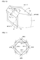
- crystal zone axis Four ⁇ 110 ⁇ planes composing the crystal zone with respect to axis [100], there are four (011), (0-11), (0-1-1) and (01-1) planes (see FIG. 11).
- the transition plane normal line angular range ⁇ specified by the normal line vectors (crystal axis orientation indices) [100] and [011] on both surfaces shown on the right of FIG. 13, contains normal line vector [111] on plane (111).
- the opening edge portion of the trench where plane (100) and plane (011) cross to each other will have plane (111) appeared therein, as shown on the left of FIG. 13. That is, the opening edge portion can be understood as a transition plane region allowing continuous change within the transition plane normal line angular range ⁇ .
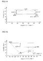
- FIG. 15 shows how the growth rate of the epitaxial layer changes within the transition plane normal line angular range ⁇ over which the plane orientation transits from (100) through (111) to (011).
- the growth rate herein is expressed by a relative value assuming the rate on plane (111) as 6. It is found from the drawing, that in-trench-wall plane (011) which falls on the originating point of the angular range ⁇ shows the largest growth rate (13 on the relative basis) out of all planes, and on the contrary, plane (111) which appears midway on the angular range ⁇ shows the smallest growth rate (6 on the relative basis) out of all planes.
- Difference ⁇ E1 in the growth rates between plane (111) composing the opening edge and substrate main plane (100) appears as 4 on the relative basis
- difference ⁇ E2 in the growth rates with respect to in-trench wall plane (011) appears as 7.
- a larger value of the sum ⁇ E1+ ⁇ E2 of the differences of the growth rates tends to give a larger growth rate at around the opening edge portion, and ⁇ E1+ ⁇ E2 in the above case appears as large as 11 on the relative basis.
- the difference ⁇ E2 in growth rates on the in-trench wall plane (011) side which largely affects the narrowing of the opening, appears especially as large as 7. That is, as shown in FIG. 10, this composes a large factor of promoting formation of the excessive growth portion 3f at the trench opening.
- the in-trench-wall plane crosses plane ⁇ 110 ⁇ at a predetermined angle, because the transition plane normal line angular range ⁇ rotates in the direction departing from the ⁇ 111> direction as expressed in the coordinate on the right of FIG. 13, so as to make plane ⁇ 111 ⁇ , allowing thereon the minimum growth rate, disappear from the transition plane region at the trench opening.
- the angle of crossing between the in-trench wall plane and plane ⁇ 110 ⁇ may be 45° or smaller.
- the angle of crossing between the in-trench wall plane and plane ⁇ 110 ⁇ is preferably set to 5° or larger, because an extremely small angle results in inclusion of a higher-index plane having a planar index close to ⁇ 111 ⁇ in the transition plane region, and makes the effect non-distinctive.
- the angle of crossing preferably coincides with any one of four ⁇ 100 ⁇ planes composing the crystal zone with respect to axis [100].
- plane ⁇ 111 ⁇ will not appear in the transition plane normal line angular range ⁇ between two these planes.
- the transition plane normal line angular range ⁇ includes the normal line on plane (110).
- FIG. 14 shows how the growth rate of the epitaxial layer varies over the transition plane normal line angular range ⁇ over which the plane orientation transits from (100) through (111) to (011). It is seen that the growth rate is maximized (becomes largest) at the position of plane (110).
- the angle of crossing of (010) composing the in-trench wall plane and the corresponding ⁇ 110 ⁇ plane is 45°.
- the growth rate within the transition plane normal line angular range ⁇ changes from that of an increasing tendency to that of a decreasing tendency.
- the intermediate section thereof may, therefore, contain an angle of crossing capable of further reducing the maximum value of the growth rate, and consequently the difference ⁇ E2 of the growth rates (or the sum ⁇ E1+ ⁇ E2), as compared with the case where the in-trench wall plane is given as (010), and at that angle, formation of the excessive growth portion may be more optimally suppressed.
- the fill-up epitaxial layer grown on the in-trench wall plane of the higher plane index may be roughened on the growth plane thereof in the process of growing, and the growth may become non-uniform against expectation.
- the in-trench wall plane having orientation ⁇ 100 ⁇ is free from such anticipation, and is sufficiently good in the suppressive effect on the formation of the excessive growth portion, so that it is still none other than an embodiment especially preferable for this invention.
- the present inventors found out that it was effective in view of making the growth of silicon uniform over the in-trench wall plane, and in view of making voids less likely to be produced in the fill-up epitaxial layer, to set the growth temperature at a lower temperature region causing no extremely sharp change in the growth rate relative to the concentration of the source gas, more specifically in a temperature range allowing the silicon deposition reaction to proceed in a reaction-rate-determining manner.
- the trenches are composed of a bottomed closed space, and in especially fine trenches (having a width of opening of 1 ⁇ m to 3 ⁇ m, and a depth of 20 ⁇ m to 50 ⁇ m, both ends inclusive) the space is substantially occupied by a diffusion region caused by friction with the inner wall planes, so that the source gas can be supplied into the trenches only by diffusion.
- the flow rate of the supplied source gas is small as shown on the left of FIG. 16
- consumption of the source gas coming by diffusion becomes relatively distinctive due to silicon deposition in the vicinity of the trench openings, and the source gas concentration becomes short around the bottom of the trenches.
- the growth rate (G.R.) is consequently reduced even in the reaction-rate-determining region, whereas the growth of silicon at the trench openings becomes relatively more likely to proceed, raising one reason for the narrowing of the openings.
- the general silicon epitaxial growth employs a carrier gas (H 2 gas, for example) at an excessive flow rate over the source gas, so that adjustments of the supply rate of the source gas correspond to adjustments of the concentration of the source gas to be supplied into the reaction vessel, and more specifically to the openings of the trenches.
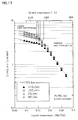
- FIG. 17 shows the Arrhenius plot of measured results of the growth rate of silicon using trichlorosilane (TCS: SiHCl 3 ) as the source gas, at various growth temperatures under the individual supply rates, while fixing the supply rate of H 2 gas as the carrier gas at 50 L/min, and varying supply rate of the source gas.
- the plots show different slopes (that are, apparent activation energies of the silicon growth reaction) in the reaction-rate-determining region on the lower temperature side and in the supply-rate-determining region on the higher temperature side.
- the transition temperature is defined as a temperature fallen on a point of intersection of regression lines, obtained by respectively subjecting the plots on the lower temperature side and on the higher temperature side on the Arrhenius plane, to a linear regression. The transition point shifts towards the higher temperature side as the supply rate of the source gas increases. From the results, it is made possible to find out the critical flow rate of the source gas as the supply rate of the source gas under which a predetermined growth temperature coincides with the transition temperature. For example, the growth temperature at around 1,000°C gives the critical flow rate of the source gas at around 11.5 L/min (this value is specific to the individual reaction vessels, and may vary depending on specifications of the vessel).
- the source gas under definition of the flow rate (supply rate) of the source gas into the reaction vessel, required for making transition temperature between the reaction rate-determining region and the supply rate-determining region with respect to silicon deposition from the source gas coincide with a predetermined growth temperature, as the critical flow rate of the source gas, the source gas is supplied into the reaction vessel at a flow rate larger than the critical flow rate of the source gas.
- the transition temperature shifts towards the higher temperature side with an increase in the supply rate of the source gas as shown in FIG. 17, so that increases in the supply rate of the source gas over the critical flow rate of the source gas means that the growth temperature is unconditionally set in the reaction-rate-determining region.
- the second aspect of the fabrication method of this invention is more effective when combined with the first aspect of the fabrication method of this invention, and can further enhance the above-described effects.
- the source gas can be supplied while keeping the pressure in the reaction vessel at normal pressure.
- Normal pressure herein means the pressure that falls within a +/-10% range around 1 ⁇ 10 5 Pa. Growth of the fill-up epitaxial layer while supplying the source gas into the reaction vessel under the normal pressure atmosphere makes it possible to raise the growth rate more than the growth under a reduced pressure atmosphere, and to improve the production efficiency.
- a larger growth rate tends to cause a larger influence of the growth rate distribution on the wall plane in fine trenches, and tends to raise a problem of residual voids and so forth, whereas adoption of the second aspect (also the first aspect as a consequence) of the fabrication method of this invention can effectively suppress such nonconformity, and can harmonize the improvement in the production efficiency and improvement in the yield ratio. This effect becomes particularly distinctive when trichlorosilane, having a large reaction efficiency for silicon deposition, is used.
- the growth inhibition gas may be a gas species suppressing decomposition reactions of the source gas, but it is more effective to adopt an etching gas for (deposited) silicon. More specifically, as shown in FIG. 18, assuming now that a gas acting as an etchant on silicon composing the in-trench wall plane is supplied alone into the trench, the depth of etching becomes larger around the trench opening, but gradually decreases towards the bottom of the trench due to consumption of the gas, as indicated by curve (A).
- the thickness of growth becomes larger at around the trench opening, but gradually decreases towards the bottom of the trench due to consumption of the gas, as indicated by curve (B).
- the concomitant supply of the source gas and the etching gas into the reaction vessel therefore, makes it possible to cancel the depth-wise distribution of the etching depth indicated by curve (A) and the depth-wise distribution of the growth thickness indicated by curve (B), so as to effectively suppress the excessive growth of silicon at around the trench opening as indicated by curve (C), to thereby allow the fill-up epitaxial layer to grow uniformly on the in-trench wall plane.
- Use of hydrogen chloride as the etching gas is preferable in view of enhancing the above-described effects.
- Japanese Laid-Open Patent Publication "Tokkai" No. 2001-196573 discloses a method of alternately repeating supply of a source gas and supply of an etching gas, but this method, based on a concept of removing, as a symptomatic treatment, the excessive growth portion by interrupting supply of the source gas and instead supplying the etching gas, is not only non-efficient, but is also unsuccessful anyhow in allowing the fill-up epitaxial layer to grown uniformly on the in-trench wall plane, because the method is on the premise that the excessive growth portion is once formed on the in-trench wall plane, and also because it is difficult to selectively remove only the excessive growth portion.
- the etching reaction For the purpose of attaining uniform growth of the fill-up epitaxial layer on the in-trench wall plane, it is essential to suppress the production of the excessive growth portion around the trench opening as much as possible, to prevent as possible inhibition of the silicon growth around the trench bottom placed under a disadvantageous condition in terms of the silicon growth as much as possible. More specifically, it is effective to allow the etching reaction to proceed in a temperature range ensuring a supply-rate-determining mode of the etching gas.
- Adoption of the temperature range ensuring a supply-rate-determining mode of the etching gas makes the etching effect rapidly appear around the opening due to a high concentration of the etching gas so as to suppress the excessive silicon deposition, whereas the etching effect rapidly reduces by the time the etching gas reaches the trench bottom side, and without interfering with the growth of the layer, because concentration of the etching gas is reduced due to consumption around the opening.
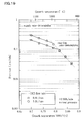
- FIG. 19 shows the Arrhenius plot of results of the etchrate of the main plane of the (100) silicon single crystal substrate using hydrogen chloride as the etching gas, measured at various etching temperatures while fixing the supply rate of H 2 gas as the carrier gas at 50 L/min, and varying the supply rate of the source gas.
- the plots clearly show the reaction-rate-determining region on the lower temperature side and the supply-rate-determining region on the higher temperature side.
- the transition temperature is again defined as a temperature fallen on a point of intersection of a regression of lines obtained by respectively subjecting the plots on the lower temperature side and on the higher temperature side on the Arrhenius plane to linear regression.
- the transition point shifts towards the higher temperature side as the supply rate of the etching gas increases, so that it is made possible to find out the critical flow rate of the etching gas as the supply rate of the etching gas under which a predetermined growth temperature coincides with the transition temperature.
- a growth temperature at around 1,000°C gives a critical flow rate of the etching gas at around 1.0 L/min (this value is specific to the individual reaction vessels, and may vary depending on the specifications of the vessel).
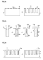
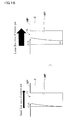
- FIG. 1 is a schematic sectional view showing an exemplary silicon epitaxial wafer of this invention.
- a silicon epitaxial wafer 1 has a structure in which a plurality of trenches 11 are formed at regular intervals, so as to align the longitudinal direction thereof with a predetermined direction, on the substrate main surface MP of an n-type silicon single crystal substrate 2 doped with P, As or Sb, and each of the inner space of the trenches 11 is filled with a fill-up epitaxial layer 3 composed of p-type silicon single crystal doped with B. Between every adjacent fill-up epitaxial layers 3, there are formed n-type layer regions 4 derived from the substrate 2.
- depth d of trench 11 is 20 ⁇ m to 50 ⁇ m, both ends inclusive
- width w1 of the trench 11 is 1 ⁇ m to 3 ⁇ m, both ends inclusive.
- width of the n-type layer region 4 (p-type layer region in FIG. 2) between every adjacent fill-up epitaxial layers 3, 3 is 1 ⁇ m to 3 ⁇ m, both ends inclusive.
- the plane index of the substrate main plane MP is (100), and the plane index of the wall plane WP of the trench 11 is (010).
- the width w1 of the opening portion of the trench 11 (fill-up epitaxial layer 3) is almost equal to width w2 at the bottom portion, where w1 may be set wider than w2 (in this case, the plane index of the wall plane WP will be higher than (010)).
- a silicon oxide film 10 is formed as a thermal oxide film, as having windows 10w for forming the trenches formed by a publicly-known photolithographic technique.
- the substrate 2 is then etched, by a dry etching process such as reactive ion etching (wet etching may be allowable, but dry etching is more preferable in view of increasing steepness of the wall plane of the trenches) from the surface exposed in the windows 10w in the depth-wise direction, to thereby form the trenches 11.
- the silicon oxide film 10 is then removed by wet etching.
- This sort of method for forming trenches is publicly known typically in Japanese Laid-Open Patent Publication "Tokkai" No. 2002-141407, and will not be detailed herein.
- a p-type silicon epitaxial layer 13 is grown in vapor phase on the substrate main plane MP side.
- the silicon single crystal substrate 2 is placed in a vapor phase growth apparatus, annealed at a predetermined temperature (at 1,130°C in a hydrogen atmosphere, for example), and thereon the fill-up epitaxial layer 3 is grown in vapor phase.
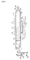
- FIG. 7 is a side-elevational sectional view of a vapor phase growth apparatus 121.
- the vapor phase growth apparatus 121 has a flat-box-type reaction vessel 122, wherein through a gas introducing port 171 formed on one end thereof, a source gas SG is supplied via a flow control section 124 into the inner space of the main vessel 123 in a horizontal-and-unidirectional manner.
- a source gas SG is supplied via a flow control section 124 into the inner space of the main vessel 123 in a horizontal-and-unidirectional manner.
- the main vessel 123 only a single wafer W is placed in a near horizontal manner on susceptor 112 placed in a susceptor housing recess 110.
- the reaction vessel 122 has, on the end portion thereof opposite to that having the source gas introducing duct 171 formed thereon, a gas discharging port 128 as being placed next to a venturi-formed drawn section 129.
- the source gas SG introduced therethrough passes over the surface of the wafer W, and is then discharged through the gas discharging port 128.
- Trichlorosilane gas is typically used as the source gas SG.
- the trichlorosilane gas is prepared as a mixed gas having a constant concentration obtained by bubbling hydrogen gas into liquid trichlorosilane (SiHCl 3 ), and is then introduced to pipe 107 while being regulated in the flow rate thereof by valve 109.
- hydrogen gas for dilution use is introduced through valve 105 into pipe 108, and both are further mixed to finally adjust the trichlorosilane concentration, and then are allowed to flow into reaction vessel 122 through source gas introducing port 171.
- a dopant gas (diborane (B 2 H 6 ) is typically used for addition of a p-type impurity intended herein) is preliminarily diluted with hydrogen gas or the like, and supplied through pipe 106 into reaction vessel 122 while being regulated in the flow rate thereof by mass flow controller (MFC) 104.
- MFC mass flow controller
- the wafer W is rotated together with susceptor 112 by a motor M, and on which an epitaxial layer is grown under supply of the source gas SB, while being heated by infrared heating lamps 111.
- Pressure in the reaction vessel 122 may be set at normal pressure, but is preferably set slightly higher than the atmospheric pressure in order to avoid sucking of the outer air.
- the growth temperature is adjusted within the range from 850°C to 1,100°C, both ends inclusive.
- a critical flow rate of the source gas required for making transition temperature between the reaction rate-determining region and the supply rate-determining region with respect to silicon deposition from tichlorosilane gas coinciding with the growth temperature, is preliminarily found out, and trichlorosilane is supplied at a flow rate larger than the critical flow rate of the source gas into reaction vessel 122.
- the supply rate of trichlorosilane into reaction vessel 122 is determined so as to obtain a trichlorosilane concentration at the bottom of the trenches 11 equal to or higher than a trichlorosilane concentration in the reaction vessel 122 when the source gas is supplied into the reaction vessel 122 at the critical flow rate of the source gas.
- a condition ranging from 18.5 L/min to 40 L/min shown in FIG. 17 is adopted.
- hydrogen chloride as the etching gas is supplied through pipe 102 into reaction vessel 122 while being regulated in the flow rate thereof by valve 103.
- a flow rate of the hydrogen chloride gas into reaction vessel 122 required for making transition temperature between the reaction rate-determining region and the supply rate-determining region with respect to silicon etching coinciding with the growth temperature as a critical flow rate of the etching gas
- the hydrogen chloride gas is supplied into reaction vessel 122 at a flow rate smaller than the critical flow rate of the etching gas.
- a condition ranging from 1.0 L/min to 0.8 L/min shown in FIG. 19 is adopted.
- the inner space of the trenches 11 is filled with a silicon epitaxial layer, which finally forms the fill-up epitaxial layer 3.
- the epitaxial layer 13 has an unnecessary grown layer 13a deposited in the region of the substrate main plane MP outside the trenches, which is removed by polishing as shown in FIG. 6, and thereby the epitaxial wafer 1 shown in FIG. 1 is completed.
- the growth rate of silicon therefore changes in the direction of decreasing as the point of observation shifts towards either the in-trench wall plane WP side or towards the substrate main plane MP side from the opening edge portion, and this successfully suppresses formation of the excessive growth portion causative of narrowing the opening of the trenches 11.
- the growth temperature is set in a low temperature range in which the growth rate does not vary in an extremely sensitive manner to trichlorosilane concentration, and more specifically, the growth temperature is set at a temperature range allowing the silicon deposition reaction to proceed based on the reaction-determining process.
- the flow rate of trichlorosilane is set considerably larger than the critical flow rate of source gas, so as to supply a sufficient concentration of trichlorosilane to the bottom of the trenches, even if the source gas is consumed to a certain extent at the upper portion of the trench openings.
- Essential Points 1 and 3 have a contribution mainly in view of suppressing formation of the excessive growth portion
- Essential Point 2 has a contribution mainly in view of promoting the growth of the fill-up epitaxial layer 3 on the trench bottom side.
- the first void 16a might be removed to a certain extent in the process of polishing the unnecessary grown layer 13a on the substrate main plane MP, if the depth of polishing is set slightly deeper, whereas the second void 16b can never be repaired once it remains, so that it is understood as extremely important to consider Essential Point 2 in the process. This makes it possible to realize the epitaxial wafer having the fill-up epitaxial layer 3 having no void 16b remained therein at a position closer to the bottom side than position d/2 (more preferably d/5).
- the in-trench wall planes combine with each other before the bottom elevates, and this makes the planar defect portion, as a trace of combination of both wall planes, more likely to be formed in the fill-up epitaxial layer, in the depth-wise direction of the trenches.
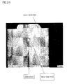
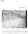
- the combination of the wall planes proceeds partially in a certain region in the depth-wise direction of the trenches, the peripheral regions left uncombined will be remained as voids. Even if such voids do not seem to remain in a macroscopic view, it is very often that a large number of dislocations and nano-size microvoids remain at the planar defect portion, as shown in TEM observation result in FIG.
- the fill-up epitaxial layer obtained in this case will have no such planar defect portion formed therein, and even if it should be formed, can readily be removed typically by polishing, because the level of the defect bottom is effectively prevented from being positioned more closer to the bottom of the trench beyond position d/5 from the opening edge.
Landscapes
- Chemical Vapour Deposition (AREA)
- Crystals, And After-Treatments Of Crystals (AREA)
Applications Claiming Priority (2)
| Application Number | Priority Date | Filing Date | Title |
|---|---|---|---|
| JP2003172269A JP3915984B2 (ja) | 2003-06-17 | 2003-06-17 | シリコンエピタキシャルウェーハの製造方法及びシリコンエピタキシャルウェーハ |
| PCT/JP2004/008135 WO2004114384A1 (fr) | 2003-06-17 | 2004-06-10 | Plaquette epitaxiale en silicium et son procede de fabrication |
Publications (2)
| Publication Number | Publication Date |
|---|---|
| EP1638136A1 true EP1638136A1 (fr) | 2006-03-22 |
| EP1638136A4 EP1638136A4 (fr) | 2010-08-04 |
Family
ID=33534671
Family Applications (1)
| Application Number | Title | Priority Date | Filing Date |
|---|---|---|---|
| EP04745765A Ceased EP1638136A4 (fr) | 2003-06-17 | 2004-06-10 | Plaquette epitaxiale en silicium et son procede de fabrication |
Country Status (4)
| Country | Link |
|---|---|
| EP (1) | EP1638136A4 (fr) |
| JP (1) | JP3915984B2 (fr) |
| CN (1) | CN100428411C (fr) |
| WO (1) | WO2004114384A1 (fr) |
Cited By (1)
| Publication number | Priority date | Publication date | Assignee | Title |
|---|---|---|---|---|
| US7410902B2 (en) | 2003-12-24 | 2008-08-12 | Kao Corporation | Composition for cleaning semiconductor device |
Families Citing this family (11)
| Publication number | Priority date | Publication date | Assignee | Title |
|---|---|---|---|---|
| JP5150048B2 (ja) * | 2005-09-29 | 2013-02-20 | 株式会社デンソー | 半導体基板の製造方法 |
| JP5015440B2 (ja) * | 2005-09-29 | 2012-08-29 | 株式会社デンソー | 半導体基板の製造方法 |
| KR100950232B1 (ko) | 2005-10-06 | 2010-03-29 | 가부시키가이샤 섬코 | 반도체 기판의 제조 방법 |
| JP4865290B2 (ja) * | 2005-10-06 | 2012-02-01 | 株式会社Sumco | 半導体基板の製造方法 |
| JP4788519B2 (ja) * | 2006-08-07 | 2011-10-05 | 株式会社デンソー | 半導体基板の製造方法 |
| JP5200604B2 (ja) * | 2008-03-19 | 2013-06-05 | 信越半導体株式会社 | スーパージャンクション構造を有する半導体素子の製造方法 |
| JP5056618B2 (ja) * | 2008-06-26 | 2012-10-24 | 豊田合成株式会社 | Iii族窒化物系化合物半導体の製造方法 |
| JP5397253B2 (ja) * | 2010-02-11 | 2014-01-22 | 株式会社デンソー | 半導体基板の製造方法 |
| JP5702622B2 (ja) * | 2011-02-14 | 2015-04-15 | 株式会社Sumco | トレンチ埋め込みエピタキシャル成長条件の最適化方法 |
| CN102693910A (zh) * | 2011-03-23 | 2012-09-26 | 上海华虹Nec电子有限公司 | 沟槽的干法刻蚀方法 |
| JP2014112594A (ja) * | 2012-12-05 | 2014-06-19 | Denso Corp | スーパージャンクション構造を有する半導体装置の製造方法 |
Family Cites Families (11)
| Publication number | Priority date | Publication date | Assignee | Title |
|---|---|---|---|---|
| US4141765A (en) * | 1975-02-17 | 1979-02-27 | Siemens Aktiengesellschaft | Process for the production of extremely flat silicon troughs by selective etching with subsequent rate controlled epitaxial refill |
| US4278987A (en) | 1977-10-17 | 1981-07-14 | Hitachi, Ltd. | Junction isolated IC with thick EPI portion having sides at least 20 degrees from (110) orientations |
| JPH05234901A (ja) * | 1992-02-19 | 1993-09-10 | Komatsu Ltd | 結晶成長方法 |
| JP3667906B2 (ja) * | 1996-11-25 | 2005-07-06 | 三洋電機株式会社 | 半導体装置及び半導体装置の製造方法 |
| JPH11135512A (ja) * | 1997-10-31 | 1999-05-21 | Mitsubishi Electric Corp | 電力用半導体装置及びその製造方法 |
| JP3485081B2 (ja) * | 1999-10-28 | 2004-01-13 | 株式会社デンソー | 半導体基板の製造方法 |
| JP4415457B2 (ja) * | 2000-06-05 | 2010-02-17 | 株式会社デンソー | 半導体装置の製造方法 |
| JP2002353451A (ja) * | 2001-05-22 | 2002-12-06 | Fuji Electric Co Ltd | 超接合半導体素子の製造方法 |
| JP2004047967A (ja) * | 2002-05-22 | 2004-02-12 | Denso Corp | 半導体装置及びその製造方法 |
| JP4304034B2 (ja) * | 2002-10-18 | 2009-07-29 | 富士電機ホールディングス株式会社 | 超接合半導体素子の製造方法 |
| JP2004141407A (ja) | 2002-10-24 | 2004-05-20 | Crecia Corp | ティシュペーパー箱 |
-
2003
- 2003-06-17 JP JP2003172269A patent/JP3915984B2/ja not_active Expired - Lifetime
-
2004
- 2004-06-10 EP EP04745765A patent/EP1638136A4/fr not_active Ceased
- 2004-06-10 WO PCT/JP2004/008135 patent/WO2004114384A1/fr not_active Ceased
- 2004-06-10 CN CNB2004800168204A patent/CN100428411C/zh not_active Expired - Lifetime
Cited By (1)
| Publication number | Priority date | Publication date | Assignee | Title |
|---|---|---|---|---|
| US7410902B2 (en) | 2003-12-24 | 2008-08-12 | Kao Corporation | Composition for cleaning semiconductor device |
Also Published As
| Publication number | Publication date |
|---|---|
| WO2004114384A1 (fr) | 2004-12-29 |
| CN1806313A (zh) | 2006-07-19 |
| CN100428411C (zh) | 2008-10-22 |
| JP2005011893A (ja) | 2005-01-13 |
| JP3915984B2 (ja) | 2007-05-16 |
| EP1638136A4 (fr) | 2010-08-04 |
Similar Documents
| Publication | Publication Date | Title |
|---|---|---|
| KR101074598B1 (ko) | 적층결함 핵생성자리들을 감소시키는 연속 리소그래피방법들과 감소된 적층결함 핵생성자리들을 포함하는 구조들 | |
| US7811907B2 (en) | Method for manufacturing semiconductor device and epitaxial growth equipment | |
| US8569106B2 (en) | Method for manufacturing silicon carbide semiconductor device | |
| US20080318359A1 (en) | Method of manufacturing silicon carbide semiconductor substrate | |
| EP1638136A1 (fr) | Plaquette epitaxiale en silicium et son procede de fabrication | |
| EP2570522A1 (fr) | Substrat monocristallin à base de carbure de silicium épitaxial et son procédé de production | |
| US20070015333A1 (en) | Method for manufacturing silicon carbide semiconductor devices | |
| CN102254796B (zh) | 形成交替排列的p型和n型半导体薄层的方法 | |
| KR101284398B1 (ko) | 적층결함 핵생성자리들을 감소시키는 리소그래피 방법들과감소된 적층결함 핵생성자리들을 포함하는 구조들 | |
| CN100565803C (zh) | 用于制造半导体器件的方法以及外延生长装置 | |
| CN112522781B (zh) | 碳化硅衬底上的缓冲层及其形成方法 | |
| US8221549B2 (en) | Silicon carbide single crystal wafer and producing method thereof | |
| US7807535B2 (en) | Methods of forming layers comprising epitaxial silicon | |
| JP4304034B2 (ja) | 超接合半導体素子の製造方法 | |
| TWI851374B (zh) | 具有超接面構造之半導體元件之製造方法 | |
| JP4215572B2 (ja) | シリコンエピタキシャルウェーハの製造方法及びシリコンエピタキシャルウェーハ | |
| JP5200604B2 (ja) | スーパージャンクション構造を有する半導体素子の製造方法 | |
| Grover et al. | Improved Angle Tolerance in 4H-SiC Trench Filling Epitaxy Using Chlorinated Chemistry | |
| KR100475547B1 (ko) | 에피 성장법을 이용한 반도체 소자의 콘택 플러그 형성 방법 | |
| JPH04372125A (ja) | 多結晶シリコンの選択成長方法 | |
| JP2007150126A (ja) | 半導体装置の製造方法 |
Legal Events
| Date | Code | Title | Description |
|---|---|---|---|
| PUAI | Public reference made under article 153(3) epc to a published international application that has entered the european phase |
Free format text: ORIGINAL CODE: 0009012 |
|
| 17P | Request for examination filed |
Effective date: 20051222 |
|
| AK | Designated contracting states |
Kind code of ref document: A1 Designated state(s): DE |
|
| DAX | Request for extension of the european patent (deleted) | ||
| RBV | Designated contracting states (corrected) |
Designated state(s): DE |
|
| RAP1 | Party data changed (applicant data changed or rights of an application transferred) |
Owner name: SHIN-ETSU HANDOTAI CO., LTD. |
|
| A4 | Supplementary search report drawn up and despatched |
Effective date: 20100701 |
|
| 17Q | First examination report despatched |
Effective date: 20101021 |
|
| RAP1 | Party data changed (applicant data changed or rights of an application transferred) |
Owner name: SHIN-ETSU HANDOTAI CO., LTD. |
|
| RAP1 | Party data changed (applicant data changed or rights of an application transferred) |
Owner name: FUJI ELECTRIC CO., LTD. |
|
| REG | Reference to a national code |
Ref country code: DE Ref legal event code: R003 |
|
| STAA | Information on the status of an ep patent application or granted ep patent |
Free format text: STATUS: THE APPLICATION HAS BEEN REFUSED |
|
| 18R | Application refused |
Effective date: 20171027 |