EP1625615B1 - Cmos-compatible integration of silicon-based optical devices with electronic devices - Google Patents
Cmos-compatible integration of silicon-based optical devices with electronic devices Download PDFInfo
- Publication number
- EP1625615B1 EP1625615B1 EP04750395.8A EP04750395A EP1625615B1 EP 1625615 B1 EP1625615 B1 EP 1625615B1 EP 04750395 A EP04750395 A EP 04750395A EP 1625615 B1 EP1625615 B1 EP 1625615B1
- Authority
- EP
- European Patent Office
- Prior art keywords
- layer
- soi
- optical
- silicon
- electrical
- Prior art date
- Legal status (The legal status is an assumption and is not a legal conclusion. Google has not performed a legal analysis and makes no representation as to the accuracy of the status listed.)
- Expired - Lifetime
Links
- 230000003287 optical effect Effects 0.000 title claims description 144
- XUIMIQQOPSSXEZ-UHFFFAOYSA-N Silicon Chemical compound [Si] XUIMIQQOPSSXEZ-UHFFFAOYSA-N 0.000 title claims description 75
- 229910052710 silicon Inorganic materials 0.000 title claims description 75
- 239000010703 silicon Substances 0.000 title claims description 75
- 230000010354 integration Effects 0.000 title description 9
- 230000007547 defect Effects 0.000 claims description 46
- 229910021332 silicide Inorganic materials 0.000 claims description 25
- FVBUAEGBCNSCDD-UHFFFAOYSA-N silicide(4-) Chemical compound [Si-4] FVBUAEGBCNSCDD-UHFFFAOYSA-N 0.000 claims description 25
- 229910052751 metal Inorganic materials 0.000 claims description 18
- 239000002184 metal Substances 0.000 claims description 18
- 239000000758 substrate Substances 0.000 claims description 13
- 238000001465 metallisation Methods 0.000 claims description 10
- 239000000463 material Substances 0.000 claims description 9
- 229910021421 monocrystalline silicon Inorganic materials 0.000 claims description 6
- 230000005670 electromagnetic radiation Effects 0.000 claims 1
- 239000010410 layer Substances 0.000 description 160
- 238000000034 method Methods 0.000 description 34
- 235000012431 wafers Nutrition 0.000 description 21
- 230000008569 process Effects 0.000 description 20
- 230000015572 biosynthetic process Effects 0.000 description 18
- 238000004519 manufacturing process Methods 0.000 description 17
- 125000006850 spacer group Chemical group 0.000 description 9
- VYPSYNLAJGMNEJ-UHFFFAOYSA-N Silicium dioxide Chemical compound O=[Si]=O VYPSYNLAJGMNEJ-UHFFFAOYSA-N 0.000 description 8
- 238000012545 processing Methods 0.000 description 8
- 229910021420 polycrystalline silicon Inorganic materials 0.000 description 7
- 229920005591 polysilicon Polymers 0.000 description 7
- 230000008878 coupling Effects 0.000 description 5
- 238000010168 coupling process Methods 0.000 description 5
- 238000005859 coupling reaction Methods 0.000 description 5
- 238000005530 etching Methods 0.000 description 5
- 238000000206 photolithography Methods 0.000 description 5
- 239000004020 conductor Substances 0.000 description 4
- 238000000151 deposition Methods 0.000 description 4
- 238000007689 inspection Methods 0.000 description 4
- 238000002955 isolation Methods 0.000 description 4
- 239000004065 semiconductor Substances 0.000 description 4
- 235000012239 silicon dioxide Nutrition 0.000 description 4
- 239000000377 silicon dioxide Substances 0.000 description 4
- 229910052581 Si3N4 Inorganic materials 0.000 description 3
- 210000000746 body region Anatomy 0.000 description 3
- 238000013461 design Methods 0.000 description 3
- 238000005516 engineering process Methods 0.000 description 3
- 239000007943 implant Substances 0.000 description 3
- 238000001459 lithography Methods 0.000 description 3
- 238000000926 separation method Methods 0.000 description 3
- HQVNEWCFYHHQES-UHFFFAOYSA-N silicon nitride Chemical compound N12[Si]34N5[Si]62N3[Si]51N64 HQVNEWCFYHHQES-UHFFFAOYSA-N 0.000 description 3
- UFHFLCQGNIYNRP-UHFFFAOYSA-N Hydrogen Chemical compound [H][H] UFHFLCQGNIYNRP-UHFFFAOYSA-N 0.000 description 2
- 238000010521 absorption reaction Methods 0.000 description 2
- 229910021417 amorphous silicon Inorganic materials 0.000 description 2
- 238000000137 annealing Methods 0.000 description 2
- 230000008901 benefit Effects 0.000 description 2
- 239000000969 carrier Substances 0.000 description 2
- 238000002425 crystallisation Methods 0.000 description 2
- 230000008025 crystallization Effects 0.000 description 2
- 230000008021 deposition Effects 0.000 description 2
- 239000003989 dielectric material Substances 0.000 description 2
- 239000002019 doping agent Substances 0.000 description 2
- 230000001747 exhibiting effect Effects 0.000 description 2
- 239000001257 hydrogen Substances 0.000 description 2
- 229910052739 hydrogen Inorganic materials 0.000 description 2
- 239000012535 impurity Substances 0.000 description 2
- 239000012212 insulator Substances 0.000 description 2
- 230000000873 masking effect Effects 0.000 description 2
- 229910052760 oxygen Inorganic materials 0.000 description 2
- 238000000059 patterning Methods 0.000 description 2
- 238000005498 polishing Methods 0.000 description 2
- 230000001902 propagating effect Effects 0.000 description 2
- 238000009877 rendering Methods 0.000 description 2
- 238000012216 screening Methods 0.000 description 2
- 239000002344 surface layer Substances 0.000 description 2
- 238000012360 testing method Methods 0.000 description 2
- 238000013459 approach Methods 0.000 description 1
- 238000000149 argon plasma sintering Methods 0.000 description 1
- QVGXLLKOCUKJST-UHFFFAOYSA-N atomic oxygen Chemical compound [O] QVGXLLKOCUKJST-UHFFFAOYSA-N 0.000 description 1
- YXTPWUNVHCYOSP-UHFFFAOYSA-N bis($l^{2}-silanylidene)molybdenum Chemical compound [Si]=[Mo]=[Si] YXTPWUNVHCYOSP-UHFFFAOYSA-N 0.000 description 1
- 229910000416 bismuth oxide Inorganic materials 0.000 description 1
- 230000008859 change Effects 0.000 description 1
- 238000006243 chemical reaction Methods 0.000 description 1
- 229910017052 cobalt Inorganic materials 0.000 description 1
- 239000010941 cobalt Substances 0.000 description 1
- GUTLYIVDDKVIGB-UHFFFAOYSA-N cobalt atom Chemical compound [Co] GUTLYIVDDKVIGB-UHFFFAOYSA-N 0.000 description 1
- 238000011109 contamination Methods 0.000 description 1
- 238000007796 conventional method Methods 0.000 description 1
- 230000002596 correlated effect Effects 0.000 description 1
- 239000013078 crystal Substances 0.000 description 1
- 238000000708 deep reactive-ion etching Methods 0.000 description 1
- 230000001066 destructive effect Effects 0.000 description 1
- 238000001514 detection method Methods 0.000 description 1
- TYIXMATWDRGMPF-UHFFFAOYSA-N dibismuth;oxygen(2-) Chemical compound [O-2].[O-2].[O-2].[Bi+3].[Bi+3] TYIXMATWDRGMPF-UHFFFAOYSA-N 0.000 description 1
- 238000009792 diffusion process Methods 0.000 description 1
- 230000000694 effects Effects 0.000 description 1
- 230000002349 favourable effect Effects 0.000 description 1
- 238000011049 filling Methods 0.000 description 1
- 229910000078 germane Inorganic materials 0.000 description 1
- 238000009499 grossing Methods 0.000 description 1
- 229910000449 hafnium oxide Inorganic materials 0.000 description 1
- WIHZLLGSGQNAGK-UHFFFAOYSA-N hafnium(4+);oxygen(2-) Chemical compound [O-2].[O-2].[Hf+4] WIHZLLGSGQNAGK-UHFFFAOYSA-N 0.000 description 1
- 238000003384 imaging method Methods 0.000 description 1
- 230000003116 impacting effect Effects 0.000 description 1
- 238000002347 injection Methods 0.000 description 1
- 239000007924 injection Substances 0.000 description 1
- 238000009413 insulation Methods 0.000 description 1
- 239000012774 insulation material Substances 0.000 description 1
- 238000005468 ion implantation Methods 0.000 description 1
- 150000002500 ions Chemical class 0.000 description 1
- 238000013508 migration Methods 0.000 description 1
- 230000005012 migration Effects 0.000 description 1
- 229910021344 molybdenum silicide Inorganic materials 0.000 description 1
- 229910021334 nickel silicide Inorganic materials 0.000 description 1
- RUFLMLWJRZAWLJ-UHFFFAOYSA-N nickel silicide Chemical compound [Ni]=[Si]=[Ni] RUFLMLWJRZAWLJ-UHFFFAOYSA-N 0.000 description 1
- 238000005457 optimization Methods 0.000 description 1
- 239000011368 organic material Substances 0.000 description 1
- 239000001301 oxygen Substances 0.000 description 1
- 238000004806 packaging method and process Methods 0.000 description 1
- 239000002245 particle Substances 0.000 description 1
- 238000002161 passivation Methods 0.000 description 1
- 230000010363 phase shift Effects 0.000 description 1
- 238000001020 plasma etching Methods 0.000 description 1
- 239000002244 precipitate Substances 0.000 description 1
- 238000011165 process development Methods 0.000 description 1
- 230000008054 signal transmission Effects 0.000 description 1
- 239000002356 single layer Substances 0.000 description 1
- 239000007787 solid Substances 0.000 description 1
- 239000007858 starting material Substances 0.000 description 1
- 239000000126 substance Substances 0.000 description 1
- 229910052715 tantalum Inorganic materials 0.000 description 1
- GUVRBAGPIYLISA-UHFFFAOYSA-N tantalum atom Chemical compound [Ta] GUVRBAGPIYLISA-UHFFFAOYSA-N 0.000 description 1
- 229910021341 titanium silicide Inorganic materials 0.000 description 1
- WQJQOUPTWCFRMM-UHFFFAOYSA-N tungsten disilicide Chemical compound [Si]#[W]#[Si] WQJQOUPTWCFRMM-UHFFFAOYSA-N 0.000 description 1
- 229910021342 tungsten silicide Inorganic materials 0.000 description 1
- 238000003631 wet chemical etching Methods 0.000 description 1
Images


Classifications
-
- H—ELECTRICITY
- H01—ELECTRIC ELEMENTS
- H01L—SEMICONDUCTOR DEVICES NOT COVERED BY CLASS H10
- H01L27/00—Devices consisting of a plurality of semiconductor or other solid-state components formed in or on a common substrate
- H01L27/02—Devices consisting of a plurality of semiconductor or other solid-state components formed in or on a common substrate including semiconductor components specially adapted for rectifying, oscillating, amplifying or switching and having at least one potential-jump barrier or surface barrier; including integrated passive circuit elements with at least one potential-jump barrier or surface barrier
- H01L27/12—Devices consisting of a plurality of semiconductor or other solid-state components formed in or on a common substrate including semiconductor components specially adapted for rectifying, oscillating, amplifying or switching and having at least one potential-jump barrier or surface barrier; including integrated passive circuit elements with at least one potential-jump barrier or surface barrier the substrate being other than a semiconductor body, e.g. an insulating body
-
- H—ELECTRICITY
- H01—ELECTRIC ELEMENTS
- H01L—SEMICONDUCTOR DEVICES NOT COVERED BY CLASS H10
- H01L27/00—Devices consisting of a plurality of semiconductor or other solid-state components formed in or on a common substrate
- H01L27/14—Devices consisting of a plurality of semiconductor or other solid-state components formed in or on a common substrate including semiconductor components sensitive to infrared radiation, light, electromagnetic radiation of shorter wavelength or corpuscular radiation and specially adapted either for the conversion of the energy of such radiation into electrical energy or for the control of electrical energy by such radiation
- H01L27/144—Devices controlled by radiation
- H01L27/146—Imager structures
- H01L27/14683—Processes or apparatus peculiar to the manufacture or treatment of these devices or parts thereof
- H01L27/14689—MOS based technologies
-
- G—PHYSICS
- G02—OPTICS
- G02B—OPTICAL ELEMENTS, SYSTEMS OR APPARATUS
- G02B6/00—Light guides; Structural details of arrangements comprising light guides and other optical elements, e.g. couplings
- G02B6/02—Optical fibres with cladding with or without a coating
-
- G—PHYSICS
- G02—OPTICS
- G02B—OPTICAL ELEMENTS, SYSTEMS OR APPARATUS
- G02B6/00—Light guides; Structural details of arrangements comprising light guides and other optical elements, e.g. couplings
- G02B6/10—Light guides; Structural details of arrangements comprising light guides and other optical elements, e.g. couplings of the optical waveguide type
- G02B6/12—Light guides; Structural details of arrangements comprising light guides and other optical elements, e.g. couplings of the optical waveguide type of the integrated circuit kind
- G02B6/12004—Combinations of two or more optical elements
-
- G—PHYSICS
- G02—OPTICS
- G02F—OPTICAL DEVICES OR ARRANGEMENTS FOR THE CONTROL OF LIGHT BY MODIFICATION OF THE OPTICAL PROPERTIES OF THE MEDIA OF THE ELEMENTS INVOLVED THEREIN; NON-LINEAR OPTICS; FREQUENCY-CHANGING OF LIGHT; OPTICAL LOGIC ELEMENTS; OPTICAL ANALOGUE/DIGITAL CONVERTERS
- G02F1/00—Devices or arrangements for the control of the intensity, colour, phase, polarisation or direction of light arriving from an independent light source, e.g. switching, gating or modulating; Non-linear optics
- G02F1/01—Devices or arrangements for the control of the intensity, colour, phase, polarisation or direction of light arriving from an independent light source, e.g. switching, gating or modulating; Non-linear optics for the control of the intensity, phase, polarisation or colour
- G02F1/015—Devices or arrangements for the control of the intensity, colour, phase, polarisation or direction of light arriving from an independent light source, e.g. switching, gating or modulating; Non-linear optics for the control of the intensity, phase, polarisation or colour based on semiconductor elements with at least one potential jump barrier, e.g. PN, PIN junction
- G02F1/025—Devices or arrangements for the control of the intensity, colour, phase, polarisation or direction of light arriving from an independent light source, e.g. switching, gating or modulating; Non-linear optics for the control of the intensity, phase, polarisation or colour based on semiconductor elements with at least one potential jump barrier, e.g. PN, PIN junction in an optical waveguide structure
-
- H—ELECTRICITY
- H01—ELECTRIC ELEMENTS
- H01L—SEMICONDUCTOR DEVICES NOT COVERED BY CLASS H10
- H01L27/00—Devices consisting of a plurality of semiconductor or other solid-state components formed in or on a common substrate
- H01L27/02—Devices consisting of a plurality of semiconductor or other solid-state components formed in or on a common substrate including semiconductor components specially adapted for rectifying, oscillating, amplifying or switching and having at least one potential-jump barrier or surface barrier; including integrated passive circuit elements with at least one potential-jump barrier or surface barrier
- H01L27/04—Devices consisting of a plurality of semiconductor or other solid-state components formed in or on a common substrate including semiconductor components specially adapted for rectifying, oscillating, amplifying or switching and having at least one potential-jump barrier or surface barrier; including integrated passive circuit elements with at least one potential-jump barrier or surface barrier the substrate being a semiconductor body
- H01L27/08—Devices consisting of a plurality of semiconductor or other solid-state components formed in or on a common substrate including semiconductor components specially adapted for rectifying, oscillating, amplifying or switching and having at least one potential-jump barrier or surface barrier; including integrated passive circuit elements with at least one potential-jump barrier or surface barrier the substrate being a semiconductor body including only semiconductor components of a single kind
- H01L27/085—Devices consisting of a plurality of semiconductor or other solid-state components formed in or on a common substrate including semiconductor components specially adapted for rectifying, oscillating, amplifying or switching and having at least one potential-jump barrier or surface barrier; including integrated passive circuit elements with at least one potential-jump barrier or surface barrier the substrate being a semiconductor body including only semiconductor components of a single kind including field-effect components only
- H01L27/088—Devices consisting of a plurality of semiconductor or other solid-state components formed in or on a common substrate including semiconductor components specially adapted for rectifying, oscillating, amplifying or switching and having at least one potential-jump barrier or surface barrier; including integrated passive circuit elements with at least one potential-jump barrier or surface barrier the substrate being a semiconductor body including only semiconductor components of a single kind including field-effect components only the components being field-effect transistors with insulated gate
- H01L27/092—Devices consisting of a plurality of semiconductor or other solid-state components formed in or on a common substrate including semiconductor components specially adapted for rectifying, oscillating, amplifying or switching and having at least one potential-jump barrier or surface barrier; including integrated passive circuit elements with at least one potential-jump barrier or surface barrier the substrate being a semiconductor body including only semiconductor components of a single kind including field-effect components only the components being field-effect transistors with insulated gate complementary MIS field-effect transistors
-
- H—ELECTRICITY
- H01—ELECTRIC ELEMENTS
- H01L—SEMICONDUCTOR DEVICES NOT COVERED BY CLASS H10
- H01L27/00—Devices consisting of a plurality of semiconductor or other solid-state components formed in or on a common substrate
- H01L27/02—Devices consisting of a plurality of semiconductor or other solid-state components formed in or on a common substrate including semiconductor components specially adapted for rectifying, oscillating, amplifying or switching and having at least one potential-jump barrier or surface barrier; including integrated passive circuit elements with at least one potential-jump barrier or surface barrier
- H01L27/12—Devices consisting of a plurality of semiconductor or other solid-state components formed in or on a common substrate including semiconductor components specially adapted for rectifying, oscillating, amplifying or switching and having at least one potential-jump barrier or surface barrier; including integrated passive circuit elements with at least one potential-jump barrier or surface barrier the substrate being other than a semiconductor body, e.g. an insulating body
- H01L27/13—Devices consisting of a plurality of semiconductor or other solid-state components formed in or on a common substrate including semiconductor components specially adapted for rectifying, oscillating, amplifying or switching and having at least one potential-jump barrier or surface barrier; including integrated passive circuit elements with at least one potential-jump barrier or surface barrier the substrate being other than a semiconductor body, e.g. an insulating body combined with thin-film or thick-film passive components
-
- H—ELECTRICITY
- H01—ELECTRIC ELEMENTS
- H01L—SEMICONDUCTOR DEVICES NOT COVERED BY CLASS H10
- H01L27/00—Devices consisting of a plurality of semiconductor or other solid-state components formed in or on a common substrate
- H01L27/14—Devices consisting of a plurality of semiconductor or other solid-state components formed in or on a common substrate including semiconductor components sensitive to infrared radiation, light, electromagnetic radiation of shorter wavelength or corpuscular radiation and specially adapted either for the conversion of the energy of such radiation into electrical energy or for the control of electrical energy by such radiation
- H01L27/144—Devices controlled by radiation
- H01L27/146—Imager structures
- H01L27/14601—Structural or functional details thereof
- H01L27/14636—Interconnect structures
-
- H—ELECTRICITY
- H01—ELECTRIC ELEMENTS
- H01L—SEMICONDUCTOR DEVICES NOT COVERED BY CLASS H10
- H01L27/00—Devices consisting of a plurality of semiconductor or other solid-state components formed in or on a common substrate
- H01L27/14—Devices consisting of a plurality of semiconductor or other solid-state components formed in or on a common substrate including semiconductor components sensitive to infrared radiation, light, electromagnetic radiation of shorter wavelength or corpuscular radiation and specially adapted either for the conversion of the energy of such radiation into electrical energy or for the control of electrical energy by such radiation
- H01L27/144—Devices controlled by radiation
- H01L27/146—Imager structures
- H01L27/14643—Photodiode arrays; MOS imagers
-
- H—ELECTRICITY
- H01—ELECTRIC ELEMENTS
- H01L—SEMICONDUCTOR DEVICES NOT COVERED BY CLASS H10
- H01L31/00—Semiconductor devices sensitive to infrared radiation, light, electromagnetic radiation of shorter wavelength or corpuscular radiation and specially adapted either for the conversion of the energy of such radiation into electrical energy or for the control of electrical energy by such radiation; Processes or apparatus specially adapted for the manufacture or treatment thereof or of parts thereof; Details thereof
- H01L31/12—Semiconductor devices sensitive to infrared radiation, light, electromagnetic radiation of shorter wavelength or corpuscular radiation and specially adapted either for the conversion of the energy of such radiation into electrical energy or for the control of electrical energy by such radiation; Processes or apparatus specially adapted for the manufacture or treatment thereof or of parts thereof; Details thereof structurally associated with, e.g. formed in or on a common substrate with, one or more electric light sources, e.g. electroluminescent light sources, and electrically or optically coupled thereto
-
- H—ELECTRICITY
- H10—SEMICONDUCTOR DEVICES; ELECTRIC SOLID-STATE DEVICES NOT OTHERWISE PROVIDED FOR
- H10N—ELECTRIC SOLID-STATE DEVICES NOT OTHERWISE PROVIDED FOR
- H10N80/00—Bulk negative-resistance effect devices
-
- H—ELECTRICITY
- H01—ELECTRIC ELEMENTS
- H01L—SEMICONDUCTOR DEVICES NOT COVERED BY CLASS H10
- H01L21/00—Processes or apparatus adapted for the manufacture or treatment of semiconductor or solid state devices or of parts thereof
- H01L21/70—Manufacture or treatment of devices consisting of a plurality of solid state components formed in or on a common substrate or of parts thereof; Manufacture of integrated circuit devices or of parts thereof
- H01L21/77—Manufacture or treatment of devices consisting of a plurality of solid state components or integrated circuits formed in, or on, a common substrate
- H01L21/78—Manufacture or treatment of devices consisting of a plurality of solid state components or integrated circuits formed in, or on, a common substrate with subsequent division of the substrate into plural individual devices
- H01L21/82—Manufacture or treatment of devices consisting of a plurality of solid state components or integrated circuits formed in, or on, a common substrate with subsequent division of the substrate into plural individual devices to produce devices, e.g. integrated circuits, each consisting of a plurality of components
- H01L21/84—Manufacture or treatment of devices consisting of a plurality of solid state components or integrated circuits formed in, or on, a common substrate with subsequent division of the substrate into plural individual devices to produce devices, e.g. integrated circuits, each consisting of a plurality of components the substrate being other than a semiconductor body, e.g. being an insulating body
-
- H—ELECTRICITY
- H01—ELECTRIC ELEMENTS
- H01L—SEMICONDUCTOR DEVICES NOT COVERED BY CLASS H10
- H01L27/00—Devices consisting of a plurality of semiconductor or other solid-state components formed in or on a common substrate
- H01L27/02—Devices consisting of a plurality of semiconductor or other solid-state components formed in or on a common substrate including semiconductor components specially adapted for rectifying, oscillating, amplifying or switching and having at least one potential-jump barrier or surface barrier; including integrated passive circuit elements with at least one potential-jump barrier or surface barrier
- H01L27/12—Devices consisting of a plurality of semiconductor or other solid-state components formed in or on a common substrate including semiconductor components specially adapted for rectifying, oscillating, amplifying or switching and having at least one potential-jump barrier or surface barrier; including integrated passive circuit elements with at least one potential-jump barrier or surface barrier the substrate being other than a semiconductor body, e.g. an insulating body
- H01L27/1203—Devices consisting of a plurality of semiconductor or other solid-state components formed in or on a common substrate including semiconductor components specially adapted for rectifying, oscillating, amplifying or switching and having at least one potential-jump barrier or surface barrier; including integrated passive circuit elements with at least one potential-jump barrier or surface barrier the substrate being other than a semiconductor body, e.g. an insulating body the substrate comprising an insulating body on a semiconductor body, e.g. SOI
Definitions
- the present invention relates to conventional CMOS-compatible fabrication techniques for silicon-based optical devices and, more particularly, to the use of CMOS-compatible fabrication techniques that allows for the integration of conventional CMOS electronic devices with silicon-based passive optical devices and active electro-optic devices in the silicon-on-insulator (SOI) structure.
- SOI silicon-on-insulator
- Integrated circuits may be fabricated on silicon-on-insulator (SOI) substrates (as compared with bulk silicon substrates) to achieve higher device speeds and/or lower power dissipation.
- SOI structure comprises a silicon substrate, a buried dielectric layer (for example, silicon dioxide) and a relatively thin (e.g., sub-micron) single crystal silicon surface layer, where this surface layer is typically referred to as the "SOI" layer.
- an SOI layer can be used as the waveguiding layer for infrared wavelengths (1.1 ⁇ m - 5.0 ⁇ m) for which silicon is nearly transparent.
- passive optical devices e.g., mirrors, rib waveguides, lenses, gratings, etc.
- the same free carriers (electrons and holes) that are used for the electronic functionality in integrated circuits can be used to actively manipulate light in silicon.
- the injection or removal of free carriers in silicon affects both the real and imaginary index of the waveguide and causes a phase shift/absorption of the light traveling through the waveguide.
- an electronic device When properly designed and combined with the confinement of light in a silicon waveguide, an electronic device can modify the optical properties of the waveguide, thus affecting the optical mode.
- SOI technology offers a powerful platform for the monolithic integration of electrical, passive optical and active electro-optical devices on a single substrate.
- CMOS complementary metal-oxide-semiconductor
- BiCMOS complementary metal-oxide-semiconductor
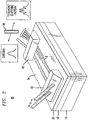
- FIG. 1 illustrates an exemplary prior art SOI-based CMOS device 10.
- a CMOS device contains a PMOS (P-channel) transistor 12 and an NMOS (N-channel) transistor 14.
- the SOI structure comprises a silicon substrate 16, a buried dielectric layer 18 and a relatively thin SOI layer 20. Electrical isolation between PMOS transistor 12 and NMOS transistor 14 is achieved by removing the portions of SOI layer 20 in the non-transistor areas, and filling these areas with a dielectric insulation material, illustrated as dielectric insulating region 22 in FIG. 1 .
- the transistors may be typically formed using the following exemplary processing steps:
- CMOS complementary metal-oxide-semiconductor
- PMOS the basic elements used in CMOS technology
- CMOS complementary metal-oxide-semiconductor
- CMOS complementary metal-oxide-semiconductor
- BiCMOS Bipolar complementary metal-oxide-semiconductor
- a channel region (such as channel regions 26 and 30 in FIG. 1 ) is formed by applying appropriate voltages to the silicide contacts of the source, drain and gate regions of the transistor.
- the conductance of the channel region, and thus the current flowing between the source and the drain is modulated by modulating the gate voltage.
- the polysilicon material is heavily doped with appropriate impurities to achieve "metal-like" electrical properties.
- the prior art describes fabrication of electro-optic devices using a relatively thick SOI layer (e.g., a few microns thick).
- a thick SOI layer limits the optical waveguide and electro-optic devices to be multi-mode, making it difficult to optimally use the free carrier-based electro-optic effect for manipulation of light.
- the bulk-like silicon region formed in the thick SOI layer due to the bulk-like silicon region formed in the thick SOI layer, the high speed and low power aspects of conventional SOI CMOS electronics cannot be achieved.
- RIE Deep reactive ion etching
- WO 03/023468 A1 discloses a strip loaded waveguide that includes a strip and a slab, wherein the strip is separated from the slab.
- a guiding region is provided for propagating an optical mode, and this guiding region extends both within the strip and the slab.
- a layer of material having an index of refraction lower than that of the strip and the slab may be disposed between and separate the strip and the slab.
- Document US2002/008217-A1 discloses a solid imaging device comprising a substrate including a semiconductor layer, a middle layer and a support layer, multiple pixels that each have a photoelectric conversion unit that includes a diffusion layer formed on the surface of the semiconductor layer, and insulating areas that are located such that they reach from the surface of the semiconductor layer to the middle layer and work together with the middle layer to electrically separate the pixels from each other.
- CMOS-compatible fabrication techniques that allow for the integration of conventional CMOS electronic devices with silicon-based passive optical devices and active electro-optic devices in a common SOI wafer.
- a wafer-scale testing is first performed to determine the quality of the SOI wafer before beginning any device fabrication, thus greatly reducing the possibility of optical defects affecting optical performance and device yield.
- the various layers associated with the electrical, passive optical, and active electro-optical components are formed using conventional CMOS processing steps.
- the various regions of the electrical devices are formed simultaneously with the optical components.
- a common dielectric and a common silicon layer are used for formation of electrical, passive optical and active electro-optical devices.
- Different regions of the common silicon layer are doped differently to achieve "metal-like" gate region for electrical, "semiconductor-like” silicon region for active electro-optic devices and "dielectric-like” silicon region for passive optical devices.
- the thin dielectric and the optical silicon layers associated with the passive optical components and active electro-optical components are first formed over an SOI substrate.
- the dielectric and silicon layers associated with the electrical components are then formed in other regions of the same SOI structure.
- One significant aspect of the present invention is the use of a common set of dielectric isolation layers, contact and via openings and metallization layers that are formed to connect various regions of the optical and electrical components. Openings for bringing optical input signals to the SOI layer are formed as the last step in the process.
- the present invention discloses a CMOS-compatible processing scheme for the fabrication of planar optical and electro-optical devices with conventional CMOS electronic devices, without significantly altering the performance of high speed/low power CMOS transistors/circuits and with high yields.
- streaking occurs when a light beam propagating along a sub-micron SOI layer encounters an optical defect of some sort. The defect perturbs the local effective refractive index of the waveguide and results in scattering, and sometimes in an interference pattern that degrades the performance of the formed optical components.
- optical defects that impact the optical performance of an SOI wafer e.g., physical defects causing optical scattering
- these optical defects may have dimension much smaller than the thickness of the "SOI" layer and can be located anywhere across the thickness of the SOI layer (e.g. sub-surface defects) and may not be detected using conventional IC defect inspection tools.
- a wafer that would allow formation of electronic components with high yield may include a large number of small optical defects, rendering the wafer unacceptable for forming optical devices with high yield.
- SOI wafer manufacturers and/or integrated circuit manufactures have not experienced any need to screen for such optical defects.
- FIG. 2 An exemplary arrangement 80 for detecting these optical streaking defects is illustrated in FIG. 2 .
- a test prism 82 is disposed on a top surface 84 of SOI layer 20 of an SOI structure being tested.
- a collimated input beam I is evanescently coupled through prism 82 and into SOI layer 20. The beam then propagates along SOI layer 20 and is subsequently evanescently coupled out of SOI layer 20 through an exit prism 86.
- a scanning slit detector 88 is disposed at the output of exit prism 86 and is used to monitor for the appearance of a "scattering" pattern in the output signal. If the shape of the output beam is distorted from its original shape (e.g.
- Physical defects that are commonly found in SOI such as crystal-originated-particles (COP) (0.1 - 0.2 ⁇ m voids - regular octahedrons surrounded by ⁇ 111 ⁇ planes with an inner wall covered by an oxide), dislocations, microcracks, defects related to oxygen precipitates, stacking faults, scratches, volume/surface contamination from organic materials, etc, can result in a localized change in refractive index, leading to streaking. From the shape of the output beam, the number, size and location of the optical defects can be estimated and then correlated to the physical defects. Once the relationship between the physical defect and the optical defect is established, well-developed physical defect identification methods can be used to determine the optical defect density.
- COP crystal-originated-particles
- the first step in the fabrication process is to screen the SOI layer to identify wafers with a low count of optical defects, where these wafers will then improve the yield of the operable optical and electro-optic devices.
- Current manufacturing methods for producing SOI wafers are only optimized for reducing electrical defects. It has been found that SOI wafers with similar specifications for electrical defects can have significantly different numbers of optical-related defects, where the number of optical-related defects has been found to depend more on the method of manufacturing used to create the SOI wafer. For example, an SOI layer prepared using an epitaxial growth process (as compared with bulk crystal formation methods) appears to have a lower density of optical defects per unit area.
- the high volume/high throughput surface light scattering inspection tools will be modified to allow for non-destructive inspection of sub-surface optical defects in the SOI layer. It is to be understood, of course, that various other techniques may be used and developed in the future to identify and inspect SOI wafers for these sub-surface optical defects. It is to be noted that optical defects with similar dimensions may result in different degree of streaking, as a function of the thickness of the SOI layer and the wavelength used for the optical device. It is expected that any defect having a dimension on the order of a predetermined fraction (e.g.
- a defect count may then be defined in terms of a unit area. For example, acceptable levels of defect count may be one defect/cm 2 , 10 defects/cm 2 , 100 defects/cm 2 etc. Of course, other fractional amounts, waveguide thicknesses and defect counts per unit area may be used to establish criteria for pre-screening of wafers, the above values being considered as exemplary only.
- a conventional MOS device is formed on SOI layer 20 in combination with a gate dielectric 34 and a silicon layer 38 (typically in the form of heavily-doped polysilicon) to form the "gate" of the structure.
- MOS metal-oxide-semiconductor
- the gate silicon layer needs to have "metal-like" electrical properties. This is achieved by degenerately doping the polysilicon layer, then forming a silicide layer on the top surface of the gate silicon layer.
- the silicon layer for the optics (hereinafter referred to as the "optical silicon layer") formed on the same SOI substrate can have any structural form (e.g., single crystal silicon, polysilicon or amorphous silicon).
- the light can be coupled between a waveguide containing only an SOI layer and a waveguide fabricated using a combination of optical silicon layer, gate dielectric and an SOI layer on the same substrate.
- An advantage of the approach of the present invention is that an "MOS" equivalent electro-optic structure is obtained in which an optical silicon layer is separated from the SOI layer by a gate dielectric layer. Both the optical silicon layer and the SOI layer can be placed with respect to one another using lithographic processes to optimally confine the light signal in the resultant waveguide.
- the shape of the optical mode is determined by various properties of the structure, such as the geometry of the layers, the thickness of the layers, the overlap between the optical silicon layer and the SOI layer and the refractive index of each layer.
- the SOI layer in combination with the gate dielectric and optical silicon layer(s) can be used to guide light and realize both high performance passive optical devices and active electro-optic devices.
- the optical silicon layer is required to have significantly different optical and electrical properties as compared with the gate silicon layer of an electrical MOS device.
- the gate silicon layer of an MOS device is degenerately doped and often silicided to have the lowest possible electrical resistance.
- the gate silicon layer is also optimized to have a minimum depletion area in the vicinity of the gate dielectric.
- these requirements result in a very high optical loss, rendering this layer useless for the formation of optical devices.
- Passive optical devices can be realized using either the SOI layer alone, or a combination of the SOI layer, a dielectric layer and the optical silicon layer.
- the optical silicon layer used in passive optical devices must exhibit relatively low optical loss, which translates into the optical silicon layer being "dielectric-like", with extremely low doping levels - essentially undoped - (to reduce free carrier absorption), large grain sizes (to reduce grain boundary scattering), smooth surfaces and sidewalls (to reduce surface scattering) and rounded corners (to minimize optical loss due to high optical density points).
- the optical silicon layer needs to have "semiconductor-like" properties, with controlled doping levels and high carrier mobility, in addition to large grain sizes, smooth surfaces and sidewalls, and rounded corners.
- optical devices cannot significantly alter the performance of standard electronic devices in order to leverage the maturity level of the design, manufacturing and cost structures of the conventional integrated circuits.
- This requires careful selection and optimization of processing time, temperature, environment and material selection for any additional process steps that may be required for the formation of passive optical devices and active electro-optic devices.
- the formation of the optical devices should use as many common steps in common with the formation of electronic devices as possible to reduce the cycle time and minimize process development costs.
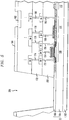
- FIG. 3 An exemplary integration of an electronic device, active electro-optic device and passive optical device, formed in accordance with the present invention, is illustrated in FIG. 3 .
- the integration is formed on a common SOI wafer 100, comprising a silicon substrate 102, buried dielectric layer 104 and surface single crystal silicon layer 106 (the latter referred to hereinafter as "SOI layer 106").
- SOI layer 106 The integration includes a PMOS electrical device 108, an active electro-optic device 110 and passive optical device 112.
- SOI layer 106 is a common foundational layer for all three types of devices and can be masked and patterned in a single lithography step to define the various regions required for each type of device.
- PMOS electrical device 108 will include a portion of SOI layer 106 labeled as "106-E", where an interior portion of region 106-E will form the body and channel of PMOS device 108, and the outer portions of 106-E will be doped with a p+ impurity to form the drain and source regions.
- a region of SOI layer 106, designated 106-A also remains after patterning and etching, and is used as part of active electro-optical device 110 (where this region may be doped to exhibit either n or p conductivity as required for a specifically desired device).
- this region may be doped to exhibit either n or p conductivity as required for a specifically desired device.
- specifically defined areas within region 106-A may be doped to exhibit certain doping profiles and contact regions to this layer can also be formed by using higher dopant concentrations.
- a region of SOI layer 106 is shown as forming part of passive optical device 112, such as a waveguide, where region 106-P is preferred to exhibit a very low doping concentration to minimize optical loss.
- a dielectric material 114 such as silicon dioxide, is thereafter formed in all exposed areas to provide electrical isolation between adjacent devices. In some cases, the structure may be re-planarized subsequent to the formation of the isolation regions.
- the next sequence of steps is used to form the device dielectric layers, where either a single layer may be formed and used for all three types of devices, or one dielectric layer may be used for the electrical devices and a second dielectric layer used for the optical devices (the differences being in thickness, material choice, or both).
- first and second dielectric layers it is preferred that the silicon layer for the optical devices is formed over the second dielectric prior to forming the first dielectric layer for the electrical devices.
- PMOS transistor 108 includes an extremely thin gate dielectric layer 116. Silicon dioxide is the most commonly used gate dielectric layer for MOS devices, and is also preferred for optical devices.
- gate dielectric materials including, but not limited to, silicon oxynitride, silicon nitride, hafnium oxide and bismuth oxide. It is preferred that relatively thin dielectric layers 118 and 120 are simultaneously formed for active electro-optical device 110 and passive optical device 112, respectively.
- a common layer(s) of silicon may be formed and used as the starting material for each type of device, with different doping levels and profiles used to form the "metal-like" gate silicon layer 122, the "semiconductor-like" active electro-optic device silicon layer 124 and the "dielectric-like" passive optical device silicon layer 126.
- a separate silicon layer(s) can be used for the optical devices and a separate silicon layer for the electrical devices, where each silicon layer may be formed using a separate set of steps, with the process conditions controlled to form the most favorable conditions for each type of device (e.g., form of silicon used, thickness of layer, doping profile, optical loss properties, etc.).
- the silicon layer associated with the electrical component gate region is heavily doped to form the "metal-like" gate.
- the silicon layer associated with the optical devices is selectively doped, as required, to form regions of different conductivities, as needed, to create various regions of optical devices, such as low-doped regions for passive devices and relatively highly doped contact regions and active carrier modulation regions for active devices, etc.
- various forms of silicon may be used for this optical silicon layer, including single crystal silicon, substantially single crystal silicon, amorphous silicon and polysilicon.
- the silicon layer may be further processed to optimize the grain size to reduce optical loss and improve electron-hole mobility (e.g., grain boundary passivated, grain aligned, grain-size enhanced polysilicon).
- the optical silicon layer may be further processed to reduce optical loss - a concern not present in the formation of electrical devices.
- a number of separate, thin silicon layers may be used to form the final optical silicon "layer" to provide the desired shape of this layer, the shape being associated with the optical mode confinement required for the device.
- a number of deposition and lithography/etching steps may be used to generate the desired geometry of the optical silicon layer.
- the silicon layer may be formed to partially overlap the SOI layer so that the optical mode peak intensity substantially coincides with the carrier modulation region, defined by the combination of the silicon layer 124, dielectric layer 118 and SOI layer 106-A.
- the sidewalls of the optical silicon layer forming both active and passive devices may be smoothed, and the corners rounded, as discussed in our co-pending application Serial No. 10/806,738, filed March 23, 2004 , to reduce optical loss.
- the passive optical devices may not require the use of any optical silicon and will use only the SOI layer to confine and manipulate the light. Since some of the optical silicon processing steps may require relatively high temperatures, it is considered prudent to form the optical devices prior to forming the electronic devices to prevent unwanted dopant migration in the electronic devices.
- a pair of sidewall spacers 128, 130 is formed adjacent to either side of metal-like gate silicon layer 122, where these spacers may comprise silicon nitride, silicon dioxide or other appropriate materials. It should be noted that this process step may result in forming unwanted spacers on the etched sidewalls of the optical device silicon layer (if the optical device silicon layer is defined prior to the formation of the electrical device sidewall spacers). These unwanted spacers can be selectively removed by using a combination of photolithography and conventional isotropic etching techniques.
- the active drain 132 and source 134 regions of PMOS transistor 108 are then formed by implant, using spacers 128 and 130 to self-align the implant areas. It is to be noted that various conventional techniques and structures are well-known and used in the formation of these device areas, including the use of a lightly-doped drain (LDD) structure, where these techniques are not considered to be germane to the subject matter of the present invention.
- LDD lightly-doped drain
- silicide process then continues with the formation of silicide contact areas for each electrical contact location for PMOS transistor 108 and active electro-optical device 110.
- a first silicide contact 136 is formed over drain region 132
- a second silicide contact 138 is formed over gate region 122
- a third silicide contact 140 is formed over source region 134.
- a first silicide contact 142 is formed over a defined contact region of silicon layer 124 and a second silicide contact 144 is formed over a defined contact region of SOI layer 106-A. Either a single silicide formation process can be used for both the electrical and optical devices, or separate processes used for each device type.
- silicide such as titanium silicide, tantalum silicide, tungsten silicide, cobalt silicide, nickel silicide or molybdenum silicide.
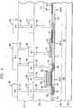
- FIG. 4 illustrates the next steps in the multi-level metallization process, the "metallization" steps including depositing a relatively thick dielectric layer over the wafer surface, opening contacts (which are then processed to be conductive) to the various contact regions, forming a first layer of metal with contacts to the contact regions, as well as forming metal line conductors, the metal line conductors interconnected as required over the dielectric layer.
- a second dielectric layer(s) is then formed, followed by forming a set of via openings, a second metal layer including electrical connection to various regions of the first metal layer, as defined by the via openings, as well as forming second level metal line conductors.
- a similar process is repeated, with the final structure thus exhibiting (if required) a "multi-level" metallization arrangement, as shown in FIG. 4 .
- a first thick dielectric layer 150 is formed to completely cover the wafer, with a plurality of contacts opened and metallized to reach each separate silicide contact.
- a plurality of conductive contacts 152, 154, 156, 158 and 160 are formed, as shown, to contact silicide regions 136, 138, 140 of PMOS transistor 108, and silicide regions 142 and 144 of active electro-optic device 110, respectively.
- a set of first-level metal line conductors 162, 164, 166, 168 and 170 are also formed (indicated as the first-level metal by the term "M-1").
- a second level of dielectric layer(s) 172 is then formed over this structure, with a set of metallized via openings 174, 176, 178 and 180 formed as shown in FIG. 4 .
- a second level of metal contacts 182, 184 and 186 is then formed, with the process of insulation/vias/contacts repeated as many times as necessary.
- the same processing steps for formation of the dielectric layers, via openings, contact openings, as well as the same metal layers are used to form the electrical connections for both the electrical devices and active electro-optic devices.
- the electro-optic devices it is preferred to maintain a predetermined separation between the metal layers and the optical confinement region to minimize optical loss. It is envisioned that design rules will be developed for ensuring that a sufficient separation is maintained. For example, cross-over of the first metal layer on the optical confinement region may be prohibited by the design rules.
- a passivation layer 190 is formed (for example, silicon nitride) and patterned to form openings for bondpad locations 192. It is a significant aspect of the present invention that well-developed bonding and packaging schemes of IC manufacturing are used to provide connections to both the electrical and active optical devices.
- a "window" 200 is opened through the entire structure down to SOI layer 106 to form the optical coupling area, that is, an area where a free space optical signal may be coupled into or out of an optical waveguide formed within SOI layer 106.
- the etching process used to open the structure must leave an "atomically smooth" surface on SOI layer 106 (smooth to within 3-4 ⁇ rms) to allow for the proper physical contact of an evanescent coupling device (e.g., prism, grating, etc - not shown) to SOI layer 106.
- an evanescent coupling device e.g., prism, grating, etc - not shown
- One such exemplary arrangement capable of providing this type of evanescent coupling is disclosed in our co-pending application Serial No. 10/668,947, filed September 23, 2003 .
- the opening of window 200 can be accomplished using a single photolithography/etch step, or can be combined with several photolithography/etch steps (for example, combining a photolithography/etch step with steps related to bondpad opening, via opening, and/or contact opening).
- a portion of the window opening process may be based on the use of wet chemical etching.
Applications Claiming Priority (3)
| Application Number | Priority Date | Filing Date | Title |
|---|---|---|---|
| US46449103P | 2003-04-21 | 2003-04-21 | |
| PCT/US2004/012236 WO2004095112A2 (en) | 2003-04-21 | 2004-04-21 | Cmos-compatible integration of silicon-based optical devices with electronic devices |
| US10/828,898 US6968110B2 (en) | 2003-04-21 | 2004-04-21 | CMOS-compatible integration of silicon-based optical devices with electronic devices |
Publications (3)
| Publication Number | Publication Date |
|---|---|
| EP1625615A2 EP1625615A2 (en) | 2006-02-15 |
| EP1625615A4 EP1625615A4 (en) | 2007-05-16 |
| EP1625615B1 true EP1625615B1 (en) | 2017-07-26 |
Family
ID=33162446
Family Applications (1)
| Application Number | Title | Priority Date | Filing Date |
|---|---|---|---|
| EP04750395.8A Expired - Lifetime EP1625615B1 (en) | 2003-04-21 | 2004-04-21 | Cmos-compatible integration of silicon-based optical devices with electronic devices |
Country Status (6)
| Country | Link |
|---|---|
| US (1) | US6968110B2 (ja) |
| EP (1) | EP1625615B1 (ja) |
| JP (1) | JP2006525677A (ja) |
| KR (1) | KR100745275B1 (ja) |
| CA (1) | CA2520972C (ja) |
| WO (1) | WO2004095112A2 (ja) |
Families Citing this family (79)
| Publication number | Priority date | Publication date | Assignee | Title |
|---|---|---|---|---|
| US7672558B2 (en) | 2004-01-12 | 2010-03-02 | Honeywell International, Inc. | Silicon optical device |
| US7013067B2 (en) * | 2004-02-11 | 2006-03-14 | Sioptical, Inc. | Silicon nanotaper couplers and mode-matching devices |
| JP4847436B2 (ja) * | 2004-02-26 | 2011-12-28 | シオプティカル インコーポレーテッド | シリコン−オン−インシュレータ(soi)構造における光の能動操作 |
| JP4847440B2 (ja) * | 2004-03-08 | 2011-12-28 | シオプティカル インコーポレーテッド | ウエハレベルでの光−電子テスト装置および方法 |
| US7217584B2 (en) | 2004-03-18 | 2007-05-15 | Honeywell International Inc. | Bonded thin-film structures for optical modulators and methods of manufacture |
| US7177489B2 (en) * | 2004-03-18 | 2007-02-13 | Honeywell International, Inc. | Silicon-insulator-silicon thin-film structures for optical modulators and methods of manufacture |
| US7149388B2 (en) * | 2004-03-18 | 2006-12-12 | Honeywell International, Inc. | Low loss contact structures for silicon based optical modulators and methods of manufacture |
| US20050214989A1 (en) * | 2004-03-29 | 2005-09-29 | Honeywell International Inc. | Silicon optoelectronic device |
| US20060063679A1 (en) * | 2004-09-17 | 2006-03-23 | Honeywell International Inc. | Semiconductor-insulator-semiconductor structure for high speed applications |
| US7109051B2 (en) * | 2004-11-15 | 2006-09-19 | Freescale Semiconductor, Inc. | Method of integrating optical devices and electronic devices on an integrated circuit |
| US20060177173A1 (en) * | 2005-02-04 | 2006-08-10 | Sioptical, Inc. | Vertical stacking of multiple integrated circuits including SOI-based optical components |
| US7538032B2 (en) * | 2005-06-23 | 2009-05-26 | Teledyne Scientific & Imaging, Llc | Low temperature method for fabricating high-aspect ratio vias and devices fabricated by said method |
| US7362443B2 (en) * | 2005-11-17 | 2008-04-22 | Honeywell International Inc. | Optical gyro with free space resonator and method for sensing inertial rotation rate |
| US7442589B2 (en) | 2006-01-17 | 2008-10-28 | Honeywell International Inc. | System and method for uniform multi-plane silicon oxide layer formation for optical applications |
| US7514285B2 (en) * | 2006-01-17 | 2009-04-07 | Honeywell International Inc. | Isolation scheme for reducing film stress in a MEMS device |
| US7463360B2 (en) | 2006-04-18 | 2008-12-09 | Honeywell International Inc. | Optical resonator gyro with integrated external cavity beam generator |
| US7454102B2 (en) * | 2006-04-26 | 2008-11-18 | Honeywell International Inc. | Optical coupling structure |
| US7535576B2 (en) | 2006-05-15 | 2009-05-19 | Honeywell International, Inc. | Integrated optical rotation sensor and method for sensing rotation rate |
| US7628932B2 (en) | 2006-06-02 | 2009-12-08 | Micron Technology, Inc. | Wet etch suitable for creating square cuts in si |
| US7709341B2 (en) * | 2006-06-02 | 2010-05-04 | Micron Technology, Inc. | Methods of shaping vertical single crystal silicon walls and resulting structures |
| US7625776B2 (en) * | 2006-06-02 | 2009-12-01 | Micron Technology, Inc. | Methods of fabricating intermediate semiconductor structures by selectively etching pockets of implanted silicon |
| US7989915B2 (en) * | 2006-07-11 | 2011-08-02 | Teledyne Licensing, Llc | Vertical electrical device |
| US7719073B2 (en) * | 2007-01-11 | 2010-05-18 | Hewlett-Packard Development Company, L.P. | Capacitively coupling layers of a multilayer device |
| US8264041B2 (en) | 2007-01-26 | 2012-09-11 | Micron Technology, Inc. | Semiconductor device with electrically floating body |
| US7829462B2 (en) * | 2007-05-03 | 2010-11-09 | Teledyne Licensing, Llc | Through-wafer vias |
| WO2009051902A1 (en) | 2007-10-17 | 2009-04-23 | Bae Systems Information And Electronic Systems Integration Inc. | Method for fabricating selectively coupled optical waveguides on a substrate |
| WO2009051903A1 (en) | 2007-10-18 | 2009-04-23 | Bae Systems Information And Electronic Systems Integration Inc. | Method for manufacturing multiple layers of waveguides |
| US7736934B2 (en) | 2007-10-19 | 2010-06-15 | Bae Systems Information And Electronic Systems Integration Inc. | Method for manufacturing vertical germanium detectors |
| US20100092682A1 (en) * | 2007-10-24 | 2010-04-15 | Bae Systems Information And Electronic Systems Int | Method for Fabricating a Heater Capable of Adjusting Refractive Index of an Optical Waveguide |
| US8343792B2 (en) | 2007-10-25 | 2013-01-01 | Bae Systems Information And Electronic Systems Integration Inc. | Method for manufacturing lateral germanium detectors |
| US7811844B2 (en) * | 2007-10-26 | 2010-10-12 | Bae Systems Information And Electronic Systems Integration Inc. | Method for fabricating electronic and photonic devices on a semiconductor substrate |
| US8031343B2 (en) * | 2007-10-29 | 2011-10-04 | Bae Systems Information And Electronic Systems Integration Inc. | High-index contrast waveguide optical gyroscope having segmented paths |
| WO2009058470A1 (en) * | 2007-10-30 | 2009-05-07 | Bae Systems Information And Electronic Systems Integration Inc. | Method for fabricating butt-coupled electro-absorptive modulators |
| US20100140587A1 (en) * | 2007-10-31 | 2010-06-10 | Carothers Daniel N | High-Injection Heterojunction Bipolar Transistor |
| WO2009115859A1 (en) * | 2008-03-19 | 2009-09-24 | S.O.I. Tec Silicon On Insulator Technologies | Substrates for monolithic optical circuits and electronic circuits |
| US7791031B2 (en) * | 2008-06-09 | 2010-09-07 | Honeywell International Inc. | Neutron detection structure |
| US20100001378A1 (en) * | 2008-07-01 | 2010-01-07 | Teledyne Scientific & Imaging, Llc | Through-substrate vias and method of fabricating same |
| US8187972B2 (en) | 2008-07-01 | 2012-05-29 | Teledyne Scientific & Imaging, Llc | Through-substrate vias with polymer fill and method of fabricating same |
| US7853101B2 (en) * | 2008-08-29 | 2010-12-14 | Bae Systems Information And Electronic Systems Integration Inc. | Bi-rate adaptive optical transfer engine |
| US7693354B2 (en) * | 2008-08-29 | 2010-04-06 | Bae Systems Information And Electronic Systems Integration Inc. | Salicide structures for heat-influenced semiconductor applications |
| US7715663B2 (en) * | 2008-08-29 | 2010-05-11 | Bae Systems Information And Electronic Systems Integration Inc. | Integrated optical latch |
| US8148265B2 (en) * | 2008-08-29 | 2012-04-03 | Bae Systems Information And Electronic Systems Integration Inc. | Two-step hardmask fabrication methodology for silicon waveguides |
| US7987066B2 (en) * | 2008-08-29 | 2011-07-26 | Bae Systems Information And Electronic Systems Integration Inc. | Components and configurations for test and valuation of integrated optical busses |
| US8288290B2 (en) * | 2008-08-29 | 2012-10-16 | Bae Systems Information And Electronic Systems Integration Inc. | Integration CMOS compatible of micro/nano optical gain materials |
| WO2010044746A1 (en) * | 2008-10-16 | 2010-04-22 | Agency For Science, Technology And Research | An integrated assembly and a method of manufacturing the same |
| US8088667B2 (en) * | 2008-11-05 | 2012-01-03 | Teledyne Scientific & Imaging, Llc | Method of fabricating vertical capacitors in through-substrate vias |
| US7847353B2 (en) * | 2008-12-05 | 2010-12-07 | Bae Systems Information And Electronic Systems Integration Inc. | Multi-thickness semiconductor with fully depleted devices and photonic integration |
| US9305779B2 (en) * | 2009-08-11 | 2016-04-05 | Bae Systems Information And Electronic Systems Integration Inc. | Method for growing germanium epitaxial films |
| US8655138B2 (en) | 2010-05-10 | 2014-02-18 | Cornell University | Waveguide structure and related fabrication method |
| WO2012075350A2 (en) * | 2010-12-03 | 2012-06-07 | Bae Systems Information And Electronic Systems Integration Inc. | Method of integrating slotted waveguide into cmos process |
| WO2012169462A1 (ja) * | 2011-06-07 | 2012-12-13 | 国立大学法人東北大学 | フォトダイオード及びその製造方法、フォトダイオードアレイ、分光光度計、並びに固体撮像装置 |
| US10094988B2 (en) | 2012-08-31 | 2018-10-09 | Micron Technology, Inc. | Method of forming photonics structures |
| US9989703B2 (en) * | 2012-11-30 | 2018-06-05 | International Business Machines Corporation | Semiconductor structure and method for manufacturing a semiconductor structure |
| GB2513531A (en) * | 2012-11-30 | 2014-11-05 | Ibm | Semiconductor structure and method for manufacturing a semiconductor structure |
| KR20140095678A (ko) * | 2013-01-25 | 2014-08-04 | 삼성전자주식회사 | 광소자 및 전자소자를 포함하는 반도체 장치 및 그 제조 방법 |
| US10222677B2 (en) | 2014-02-24 | 2019-03-05 | Rockley Photonics Limited | Optoelectronic device |
| US10928659B2 (en) | 2014-02-24 | 2021-02-23 | Rockley Photonics Limited | Optoelectronic device |
| EP3111261A2 (en) | 2014-02-24 | 2017-01-04 | Rockley Photonics Limited | Detector remodulator and optoelectronic switch |
| GB2523383B (en) * | 2014-02-24 | 2016-09-14 | Rockley Photonics Ltd | Detector remodulator |
| GB2564158B (en) | 2017-07-05 | 2019-12-18 | Rockley Photonics Ltd | Optoelectronic device |
| WO2016023105A1 (en) * | 2014-08-15 | 2016-02-18 | Aeponyx Inc. | Methods and systems for microelectromechanical packaging |
| EP3035092B1 (en) * | 2014-12-16 | 2020-05-20 | IMEC vzw | Integrated semiconductor optical coupler. |
| US10216059B2 (en) | 2015-03-05 | 2019-02-26 | Rockley Photonics Limited | Waveguide modulator structures |
| US10678115B2 (en) | 2015-03-05 | 2020-06-09 | Rockley Photonics Limited | Waveguide modulator structures |
| CN107533248A (zh) | 2015-03-05 | 2018-01-02 | 洛克利光子有限公司 | 波导调制器结构 |
| US11150494B2 (en) | 2015-03-05 | 2021-10-19 | Rockley Photonics Limited | Waveguide modulator structures |
| US10025033B2 (en) | 2016-03-01 | 2018-07-17 | Advanced Semiconductor Engineering, Inc. | Optical fiber structure, optical communication apparatus and manufacturing process for manufacturing the same |
| US10241264B2 (en) | 2016-07-01 | 2019-03-26 | Advanced Semiconductor Engineering, Inc. | Semiconductor device packages |
| US11101256B2 (en) | 2016-11-23 | 2021-08-24 | Rockley Photonics Limited | Optical modulators |
| US11022824B2 (en) * | 2016-11-23 | 2021-06-01 | Rockley Photonics Limited | Electro-optically active device |
| US11105975B2 (en) * | 2016-12-02 | 2021-08-31 | Rockley Photonics Limited | Waveguide optoelectronic device |
| WO2018100172A1 (en) | 2016-12-02 | 2018-06-07 | Rockley Photonics Limited | Waveguide device and method of doping a waveguide device |
| US10197730B1 (en) | 2017-11-08 | 2019-02-05 | Globalfoundries Inc. | Optical through silicon via |
| EP3714321B1 (en) * | 2017-11-23 | 2023-12-13 | Rockley Photonics Limited | Electro-optically active device |
| KR102590996B1 (ko) * | 2018-10-17 | 2023-10-17 | 삼성전자주식회사 | 반도체 장치 |
| US10509244B1 (en) * | 2018-12-11 | 2019-12-17 | Globalfoundries Inc. | Optical switches and routers operated by phase-changing materials controlled by heaters |
| US11899242B2 (en) * | 2020-03-27 | 2024-02-13 | Taiwan Semiconductor Manufacturing Co., Ltd. | Method of manufacturing a packaged device with optical pathway |
| US11592618B2 (en) | 2020-06-10 | 2023-02-28 | Taiwan Semiconductor Manufacturing Co., Ltd. | Photonic semiconductor device and method of manufacture |
| CN117199155B (zh) * | 2023-11-06 | 2024-02-13 | 杭州特洛伊光电技术有限公司 | 一种波导型可见光及近红外光探测器结构与制备方法 |
Family Cites Families (21)
| Publication number | Priority date | Publication date | Assignee | Title |
|---|---|---|---|---|
| JPH0287581A (ja) * | 1988-09-26 | 1990-03-28 | Canon Inc | 波長分波光検出器 |
| US4958898A (en) * | 1989-03-15 | 1990-09-25 | The United States Of America As Represented By The Secretary Of The Air Force | Silicon double-injection electro-optic modulator with insulated-gate and method of using same |
| JP3363561B2 (ja) * | 1993-03-01 | 2003-01-08 | セイコーインスツルメンツ株式会社 | 接合型電界効果トランジスタ |
| DE19503641A1 (de) * | 1995-02-06 | 1996-08-08 | Forschungszentrum Juelich Gmbh | Schichtstruktur mit einer Silicid-Schicht, sowie Verfahren zur Herstellung einer solchen Schichtstruktur |
| US6020581A (en) * | 1998-02-24 | 2000-02-01 | International Business Machines Corporation | Solid state CMOS imager using silicon-on-insulator or bulk silicon |
| JPH11330473A (ja) * | 1998-05-12 | 1999-11-30 | Hitachi Ltd | 半導体集積回路装置およびその製造方法 |
| JP3358550B2 (ja) | 1998-07-07 | 2002-12-24 | 信越半導体株式会社 | Soiウエーハの製造方法ならびにこの方法で製造されるsoiウエーハ |
| JP4860026B2 (ja) * | 1999-03-03 | 2012-01-25 | 株式会社半導体エネルギー研究所 | 表示装置 |
| JP2000298218A (ja) * | 1999-04-13 | 2000-10-24 | Hitachi Ltd | 光インターコネクト装置およびその製造方法 |
| US6653209B1 (en) | 1999-09-30 | 2003-11-25 | Canon Kabushiki Kaisha | Method of producing silicon thin film, method of constructing SOI substrate and semiconductor device |
| KR100730806B1 (ko) | 1999-10-14 | 2007-06-20 | 신에쯔 한도타이 가부시키가이샤 | Soi웨이퍼의 제조방법 및 soi 웨이퍼 |
| JP4797221B2 (ja) * | 2000-02-21 | 2011-10-19 | ソニー株式会社 | 光電子集積回路装置 |
| JP2001326343A (ja) * | 2000-05-16 | 2001-11-22 | Minolta Co Ltd | 固体撮像装置 |
| JP2002033399A (ja) * | 2000-07-13 | 2002-01-31 | Toshiba Corp | 半導体集積回路及びその製造方法 |
| JP2002110688A (ja) | 2000-09-29 | 2002-04-12 | Canon Inc | Soiの熱処理方法及び製造方法 |
| JP2002299598A (ja) * | 2001-04-03 | 2002-10-11 | Fujitsu Ltd | 半導体装置 |
| US6912330B2 (en) * | 2001-05-17 | 2005-06-28 | Sioptical Inc. | Integrated optical/electronic circuits and associated methods of simultaneous generation thereof |
| WO2002093203A2 (en) | 2001-05-17 | 2002-11-21 | Optronx, Inc | Integrated optical/electronic circuits and associated methods of simultaneous generation thereof |
| US6990257B2 (en) * | 2001-09-10 | 2006-01-24 | California Institute Of Technology | Electronically biased strip loaded waveguide |
| JP2003188223A (ja) | 2001-12-19 | 2003-07-04 | Mitsubishi Electric Corp | 結晶欠陥の顕在化方法、評価用半導体装置の製造方法、結晶欠陥の評価方法及び、評価用半導体装置 |
| US6813431B2 (en) * | 2002-02-26 | 2004-11-02 | Intel Corporation | Integrated photodevice and waveguide |
-
2004
- 2004-04-21 JP JP2006513175A patent/JP2006525677A/ja active Pending
- 2004-04-21 US US10/828,898 patent/US6968110B2/en not_active Expired - Lifetime
- 2004-04-21 EP EP04750395.8A patent/EP1625615B1/en not_active Expired - Lifetime
- 2004-04-21 KR KR1020057020085A patent/KR100745275B1/ko active IP Right Grant
- 2004-04-21 CA CA2520972A patent/CA2520972C/en not_active Expired - Fee Related
- 2004-04-21 WO PCT/US2004/012236 patent/WO2004095112A2/en active Application Filing
Non-Patent Citations (1)
| Title |
|---|
| None * |
Also Published As
| Publication number | Publication date |
|---|---|
| KR20060003046A (ko) | 2006-01-09 |
| CA2520972A1 (en) | 2004-11-04 |
| WO2004095112A3 (en) | 2005-03-31 |
| EP1625615A2 (en) | 2006-02-15 |
| JP2006525677A (ja) | 2006-11-09 |
| US20040207016A1 (en) | 2004-10-21 |
| KR100745275B1 (ko) | 2007-08-01 |
| WO2004095112A2 (en) | 2004-11-04 |
| US6968110B2 (en) | 2005-11-22 |
| CA2520972C (en) | 2010-01-26 |
| EP1625615A4 (en) | 2007-05-16 |
Similar Documents
| Publication | Publication Date | Title |
|---|---|---|
| EP1625615B1 (en) | Cmos-compatible integration of silicon-based optical devices with electronic devices | |
| US20050236619A1 (en) | CMOS-compatible integration of silicon-based optical devices with electronic devices | |
| Assefa et al. | CMOS-integrated high-speed MSM germanium waveguide photodetector | |
| US7397101B1 (en) | Germanium silicon heterostructure photodetectors | |
| US7266263B2 (en) | Integrated waveguide photodetector apparatus with matching propagation constants and related coupling methods | |
| US20070104411A1 (en) | Vertically-integrated waveguide photodetector apparatus and related coupling methods | |
| US10043925B2 (en) | Guided-wave photodetector apparatus employing mid-bandgap states of semiconductor materials, and fabrication methods for same | |
| EP1946169A1 (en) | Laterally-integrated waveguide photodetector apparatus and related coupling methods | |
| TWI396277B (zh) | 形成半導體裝置與光學裝置之方法及其結構 | |
| US20210135025A1 (en) | Method and optoelectronic structure providing polysilicon photonic devices with different optical properties in different regions | |
| US8232586B2 (en) | Silicon photon detector | |
| US11105974B2 (en) | Waveguide-coupled silicon-germanium photodetectors and fabrication methods for same | |
| KR20060040711A (ko) | 써멀 버짓에 대한 솔루션 | |
| US7526146B1 (en) | Electro-optical modulator and a method for manufacturing the same | |
| US8138579B2 (en) | Structures and methods of forming SiGe and SiGeC buried layer for SOI/SiGe technology | |
| US20060091461A1 (en) | Transistor structure with dual trench for optimized stress effect and method therefor | |
| CN100399536C (zh) | 带有电设备的硅基光设备的cmos兼容集成 | |
| US8048705B2 (en) | Method and structure for a CMOS image sensor using a triple gate process | |
| Xu | Germanium-Tin Photo Detectors for Applications in the Two Micron Wavelength Range | |
| US9395490B2 (en) | Variable buried oxide thickness for a waveguide | |
| US20030096440A1 (en) | Method for forming a semiconductor device for detecting light | |
| KR100584124B1 (ko) | 반도체 소자용 기판 제조 방법 및 이를 이용한 반도체소자의 제조방법 | |
| US20100197066A1 (en) | Method of interconnect for image sensor | |
| Csutak | Optical receivers and photodetectors in 130nm CMOS technology | |
| Lee | CMOS backend deposited silicon photonics-material, design, and integration |
Legal Events
| Date | Code | Title | Description |
|---|---|---|---|
| PUAI | Public reference made under article 153(3) epc to a published international application that has entered the european phase |
Free format text: ORIGINAL CODE: 0009012 |
|
| 17P | Request for examination filed |
Effective date: 20051121 |
|
| AK | Designated contracting states |
Kind code of ref document: A2 Designated state(s): DE FR GB IT SE |
|
| DAX | Request for extension of the european patent (deleted) | ||
| RBV | Designated contracting states (corrected) |
Designated state(s): DE FR GB IT SE |
|
| A4 | Supplementary search report drawn up and despatched |
Effective date: 20070417 |
|
| RIC1 | Information provided on ipc code assigned before grant |
Ipc: H01L 27/146 20060101ALI20070411BHEP Ipc: H01L 21/76 20060101AFI20051122BHEP |
|
| 17Q | First examination report despatched |
Effective date: 20070719 |
|
| RAP1 | Party data changed (applicant data changed or rights of an application transferred) |
Owner name: PATEL, VIPULKUMAR Owner name: SHASTRI, KALPENDU Owner name: YANUSHEFSKI, KATHERINE A. Owner name: GOTHOSKAR, PRAKASH Owner name: GHIRON, MARGARET Owner name: CISCO TECHNOLOGY, INC. Owner name: PATHAK, SOHAM Owner name: MONTGOMERY, ROBERT KEITH |
|
| RAP1 | Party data changed (applicant data changed or rights of an application transferred) |
Owner name: CISCO TECHNOLOGY, INC. |
|
| GRAP | Despatch of communication of intention to grant a patent |
Free format text: ORIGINAL CODE: EPIDOSNIGR1 |
|
| STAA | Information on the status of an ep patent application or granted ep patent |
Free format text: STATUS: GRANT OF PATENT IS INTENDED |
|
| RIC1 | Information provided on ipc code assigned before grant |
Ipc: G02B 6/12 20060101ALN20170209BHEP Ipc: H01L 27/13 20060101ALN20170209BHEP Ipc: H01L 27/12 20060101ALN20170209BHEP Ipc: G02F 1/025 20060101ALN20170209BHEP Ipc: H01L 21/84 20060101ALI20170209BHEP Ipc: H01L 27/146 20060101ALI20170209BHEP Ipc: H01L 31/12 20060101ALI20170209BHEP Ipc: H01L 21/76 20060101AFI20170209BHEP |
|
| INTG | Intention to grant announced |
Effective date: 20170227 |
|
| GRAS | Grant fee paid |
Free format text: ORIGINAL CODE: EPIDOSNIGR3 |
|
| GRAA | (expected) grant |
Free format text: ORIGINAL CODE: 0009210 |
|
| STAA | Information on the status of an ep patent application or granted ep patent |
Free format text: STATUS: THE PATENT HAS BEEN GRANTED |
|
| AK | Designated contracting states |
Kind code of ref document: B1 Designated state(s): DE FR GB IT SE |
|
| REG | Reference to a national code |
Ref country code: GB Ref legal event code: FG4D |
|
| REG | Reference to a national code |
Ref country code: DE Ref legal event code: R096 Ref document number: 602004051584 Country of ref document: DE |
|
| PG25 | Lapsed in a contracting state [announced via postgrant information from national office to epo] |
Ref country code: SE Free format text: LAPSE BECAUSE OF FAILURE TO SUBMIT A TRANSLATION OF THE DESCRIPTION OR TO PAY THE FEE WITHIN THE PRESCRIBED TIME-LIMIT Effective date: 20170726 |
|
| REG | Reference to a national code |
Ref country code: FR Ref legal event code: PLFP Year of fee payment: 15 |
|
| REG | Reference to a national code |
Ref country code: DE Ref legal event code: R097 Ref document number: 602004051584 Country of ref document: DE |
|
| PG25 | Lapsed in a contracting state [announced via postgrant information from national office to epo] |
Ref country code: IT Free format text: LAPSE BECAUSE OF FAILURE TO SUBMIT A TRANSLATION OF THE DESCRIPTION OR TO PAY THE FEE WITHIN THE PRESCRIBED TIME-LIMIT Effective date: 20170726 |
|
| PLBE | No opposition filed within time limit |
Free format text: ORIGINAL CODE: 0009261 |
|
| STAA | Information on the status of an ep patent application or granted ep patent |
Free format text: STATUS: NO OPPOSITION FILED WITHIN TIME LIMIT |
|
| 26N | No opposition filed |
Effective date: 20180430 |
|
| PGFP | Annual fee paid to national office [announced via postgrant information from national office to epo] |
Ref country code: FR Payment date: 20200427 Year of fee payment: 17 |
|
| PG25 | Lapsed in a contracting state [announced via postgrant information from national office to epo] |
Ref country code: FR Free format text: LAPSE BECAUSE OF NON-PAYMENT OF DUE FEES Effective date: 20210430 |
|
| P01 | Opt-out of the competence of the unified patent court (upc) registered |
Effective date: 20230525 |
|
| PGFP | Annual fee paid to national office [announced via postgrant information from national office to epo] |
Ref country code: DE Payment date: 20230421 Year of fee payment: 20 |
|
| PGFP | Annual fee paid to national office [announced via postgrant information from national office to epo] |
Ref country code: GB Payment date: 20230425 Year of fee payment: 20 |
|
| REG | Reference to a national code |
Ref country code: DE Ref legal event code: R071 Ref document number: 602004051584 Country of ref document: DE |