EP1624485B1 - Verfahren zur Herstellung einer organischen Elektrolumineszenzanzeige - Google Patents
Verfahren zur Herstellung einer organischen Elektrolumineszenzanzeige Download PDFInfo
- Publication number
- EP1624485B1 EP1624485B1 EP05077308A EP05077308A EP1624485B1 EP 1624485 B1 EP1624485 B1 EP 1624485B1 EP 05077308 A EP05077308 A EP 05077308A EP 05077308 A EP05077308 A EP 05077308A EP 1624485 B1 EP1624485 B1 EP 1624485B1
- Authority
- EP
- European Patent Office
- Prior art keywords
- layer
- organic
- display device
- manufacturing
- electrode
- Prior art date
- Legal status (The legal status is an assumption and is not a legal conclusion. Google has not performed a legal analysis and makes no representation as to the accuracy of the status listed.)
- Expired - Lifetime
Links
Images


Classifications
-
- H—ELECTRICITY
- H05—ELECTRIC TECHNIQUES NOT OTHERWISE PROVIDED FOR
- H05B—ELECTRIC HEATING; ELECTRIC LIGHT SOURCES NOT OTHERWISE PROVIDED FOR; CIRCUIT ARRANGEMENTS FOR ELECTRIC LIGHT SOURCES, IN GENERAL
- H05B33/00—Electroluminescent light sources
- H05B33/10—Apparatus or processes specially adapted to the manufacture of electroluminescent light sources
-
- H—ELECTRICITY
- H10—SEMICONDUCTOR DEVICES; ELECTRIC SOLID-STATE DEVICES NOT OTHERWISE PROVIDED FOR
- H10K—ORGANIC ELECTRIC SOLID-STATE DEVICES
- H10K50/00—Organic light-emitting devices
- H10K50/80—Constructional details
- H10K50/805—Electrodes
- H10K50/82—Cathodes
-
- H—ELECTRICITY
- H10—SEMICONDUCTOR DEVICES; ELECTRIC SOLID-STATE DEVICES NOT OTHERWISE PROVIDED FOR
- H10K—ORGANIC ELECTRIC SOLID-STATE DEVICES
- H10K59/00—Integrated devices, or assemblies of multiple devices, comprising at least one organic light-emitting element covered by group H10K50/00
- H10K59/10—OLED displays
- H10K59/17—Passive-matrix OLED displays
-
- H—ELECTRICITY
- H10—SEMICONDUCTOR DEVICES; ELECTRIC SOLID-STATE DEVICES NOT OTHERWISE PROVIDED FOR
- H10K—ORGANIC ELECTRIC SOLID-STATE DEVICES
- H10K71/00—Manufacture or treatment specially adapted for the organic devices covered by this subclass
- H10K71/10—Deposition of organic active material
- H10K71/18—Deposition of organic active material using non-liquid printing techniques, e.g. thermal transfer printing from a donor sheet
-
- H—ELECTRICITY
- H10—SEMICONDUCTOR DEVICES; ELECTRIC SOLID-STATE DEVICES NOT OTHERWISE PROVIDED FOR
- H10K—ORGANIC ELECTRIC SOLID-STATE DEVICES
- H10K59/00—Integrated devices, or assemblies of multiple devices, comprising at least one organic light-emitting element covered by group H10K50/00
- H10K59/30—Devices specially adapted for multicolour light emission
- H10K59/35—Devices specially adapted for multicolour light emission comprising red-green-blue [RGB] subpixels
-
- H—ELECTRICITY
- H10—SEMICONDUCTOR DEVICES; ELECTRIC SOLID-STATE DEVICES NOT OTHERWISE PROVIDED FOR
- H10K—ORGANIC ELECTRIC SOLID-STATE DEVICES
- H10K71/00—Manufacture or treatment specially adapted for the organic devices covered by this subclass
-
- H—ELECTRICITY
- H10—SEMICONDUCTOR DEVICES; ELECTRIC SOLID-STATE DEVICES NOT OTHERWISE PROVIDED FOR
- H10K—ORGANIC ELECTRIC SOLID-STATE DEVICES
- H10K71/00—Manufacture or treatment specially adapted for the organic devices covered by this subclass
- H10K71/10—Deposition of organic active material
- H10K71/12—Deposition of organic active material using liquid deposition, e.g. spin coating
- H10K71/13—Deposition of organic active material using liquid deposition, e.g. spin coating using printing techniques, e.g. ink-jet printing or screen printing
- H10K71/135—Deposition of organic active material using liquid deposition, e.g. spin coating using printing techniques, e.g. ink-jet printing or screen printing using ink-jet printing
-
- H—ELECTRICITY
- H10—SEMICONDUCTOR DEVICES; ELECTRIC SOLID-STATE DEVICES NOT OTHERWISE PROVIDED FOR
- H10K—ORGANIC ELECTRIC SOLID-STATE DEVICES
- H10K71/00—Manufacture or treatment specially adapted for the organic devices covered by this subclass
- H10K71/50—Forming devices by joining two substrates together, e.g. lamination techniques
-
- H—ELECTRICITY
- H10—SEMICONDUCTOR DEVICES; ELECTRIC SOLID-STATE DEVICES NOT OTHERWISE PROVIDED FOR
- H10K—ORGANIC ELECTRIC SOLID-STATE DEVICES
- H10K71/00—Manufacture or treatment specially adapted for the organic devices covered by this subclass
- H10K71/60—Forming conductive regions or layers, e.g. electrodes
- H10K71/611—Forming conductive regions or layers, e.g. electrodes using printing deposition, e.g. ink jet printing
-
- H—ELECTRICITY
- H10—SEMICONDUCTOR DEVICES; ELECTRIC SOLID-STATE DEVICES NOT OTHERWISE PROVIDED FOR
- H10K—ORGANIC ELECTRIC SOLID-STATE DEVICES
- H10K85/00—Organic materials used in the body or electrodes of devices covered by this subclass
- H10K85/10—Organic polymers or oligomers
- H10K85/111—Organic polymers or oligomers comprising aromatic, heteroaromatic, or aryl chains, e.g. polyaniline, polyphenylene or polyphenylene vinylene
- H10K85/114—Poly-phenylenevinylene; Derivatives thereof
-
- H—ELECTRICITY
- H10—SEMICONDUCTOR DEVICES; ELECTRIC SOLID-STATE DEVICES NOT OTHERWISE PROVIDED FOR
- H10K—ORGANIC ELECTRIC SOLID-STATE DEVICES
- H10K85/00—Organic materials used in the body or electrodes of devices covered by this subclass
- H10K85/10—Organic polymers or oligomers
- H10K85/111—Organic polymers or oligomers comprising aromatic, heteroaromatic, or aryl chains, e.g. polyaniline, polyphenylene or polyphenylene vinylene
- H10K85/115—Polyfluorene; Derivatives thereof
-
- H—ELECTRICITY
- H10—SEMICONDUCTOR DEVICES; ELECTRIC SOLID-STATE DEVICES NOT OTHERWISE PROVIDED FOR
- H10K—ORGANIC ELECTRIC SOLID-STATE DEVICES
- H10K85/00—Organic materials used in the body or electrodes of devices covered by this subclass
- H10K85/30—Coordination compounds
-
- H—ELECTRICITY
- H10—SEMICONDUCTOR DEVICES; ELECTRIC SOLID-STATE DEVICES NOT OTHERWISE PROVIDED FOR
- H10K—ORGANIC ELECTRIC SOLID-STATE DEVICES
- H10K85/00—Organic materials used in the body or electrodes of devices covered by this subclass
- H10K85/30—Coordination compounds
- H10K85/321—Metal complexes comprising a group IIIA element, e.g. Tris (8-hydroxyquinoline) gallium [Gaq3]
- H10K85/324—Metal complexes comprising a group IIIA element, e.g. Tris (8-hydroxyquinoline) gallium [Gaq3] comprising aluminium, e.g. Alq3
-
- H—ELECTRICITY
- H10—SEMICONDUCTOR DEVICES; ELECTRIC SOLID-STATE DEVICES NOT OTHERWISE PROVIDED FOR
- H10K—ORGANIC ELECTRIC SOLID-STATE DEVICES
- H10K85/00—Organic materials used in the body or electrodes of devices covered by this subclass
- H10K85/60—Organic compounds having low molecular weight
- H10K85/631—Amine compounds having at least two aryl rest on at least one amine-nitrogen atom, e.g. triphenylamine
Definitions
- the present invention relates to a method for manufacturing an organic EL display device which is used in emissive simple matrix drive-type medium or large volume monochromatic or color displays, camcorder or digital camera view finders, and the like.
- the structure of most conventional organic EL elements comprises a transparent electrode formed on a glass substrate, where light is transmitted through the glass substrate.
- the penetration through the glass substrate results in outgoing radiation, and thus in greater light leakage in the direction of the substrate plane, allowing only 20% of the total light emission to be used.
- An object of the present invention is to provide a method for the extremely simple patterning of electrodes and light emitting layers in methods for manufacturing organic EL display devices, and to provide such a method in which all the light emission is radiated outward in the direction of the visual field without being wasted.
- the method for manufacturing an organic EL display device in the present invention is a method for manufacturing an organic EL display device which is used in simple matrix drives, characterized in that a light-heat conversion layer and heat-propagating layer are formed on a film, a cathode layer is then formed, a light emitting layer is then formed thereon, a positive hole-injecting layer is then formed thereon, the film on which these multiple layers have been formed is then placed in contact with a substrate with a stripe-patterned ITO, the aforementioned multiple layers are transferred onto the substrate by irradiating the other side of the film with a laser in such a way as to form the shape of the cathode, the film is then removed, a drive mechanism is connected to the substrate onto which the aforementioned multiple layers have been transferred, and a sealing process is carried out.
- This structure allows cathodes which are extremely unstable and difficult to pattern to be readily patterned simultaneously with the transfer of the organic EL layer by laser.
- the method for manufacturing an organic EL display device in the present invention is a method for manufacturing an organic EL display device which is used in simple matrix drives, characterized in that a light-heat conversion layer and heat-propagating layer are formed on a film, a cathode layer is then formed, an electroluminescent adhesive layer is then formed thereon, the film on which these multiple layers have been formed is then placed in contact with a substrate with a stripe-patterned ITO, the aforementioned multiple layers are transferred onto the substrate by irradiating the other side of the film with a laser in such a way as to form the shape of the cathode, the film is then removed, a drive mechanism is connected to the substrate onto which the multiple layers have been transferred, and a sealing process is carried out.
- This structure allows cathodes with a simple structure, which are extremely unstable and difficult to pattern, to be readily patterned simultaneously with the transfer of the organic EL layer by laser.
- Means 3 for solving the problem This is characterized in that an electron-injecting layer is formed between the cathode layer and light emitting layer of the first means for solving the problem or between the cathode layer and the electroluminescent adhesive layer of the second means for solving the problem. This allows the luminous efficiency to be improved in the aforementioned structures.
- Means 4 for solving the problem The method for manufacturing an organic EL display device that is used in simple matrix drives is characterized in that a light-heat conversion layer and heat-propagating layer are formed on a film, an anode layer is then formed, a positive hole-injecting layer is then formed thereon, a light emitting layer is then formed thereon, an electron-injecting adhesive layer is then formed thereon, the film on which these multiple layers have been formed is then placed in contact with a substrate with a patterned cathode, the other side of the film is irradiated with a laser in such a way as to form the shape of the cathode, the film is then removed, a drive mechanism is connected to the substrate onto which the aforementioned multiple layers have been transferred, and a sealing process is carried out.
- This structure allows cathodes which are difficult to pattern to be readily patterned by means of a laser or the like after being formed on a glass substrate, and also allows anodes to be patterned simultaneously during the subsequent transfer of the organic EL layer. This structure also allows light to be directly transmitted to the outside without passing through the glass substrate from the organic light emitting layer, so that no light is lost, resulting in better brightness.
- Means 5 for solving the problem The method for manufacturing an organic EL display device that is used in simple matrix drives is characterized in that a light-heat conversion layer and heat-propagating layer are formed on a film, an anode layer is then formed, a positive hole-injecting layer is then formed thereon, an electroluminescent adhesive layer is then formed thereon, the film on which these multiple layers have been formed is then placed in contact with a substrate with a patterned cathode, the other side of the film is irradiated with a laser in such a way as to form the shape of the cathode, the film is then removed, a drive mechanism is connected to the substrate onto which the aforementioned multiple layers have been transferred, and a sealing process is carried out.
- This structure allows cathodes which are difficult to pattern to be readily patterned by means of a laser or the like after being formed on a glass substrate, and also allows anodes to be patterned simultaneously during the subsequent transfer of the organic EL layer.
- the manufacturing process is also simplified because the adhesive layer also has a light-emitting function.
- This structure also allows light to be directly transmitted to the outside without passing through the glass substrate from the organic light emitting layer, so that no light is lost, resulting in better brightness.
- Means 6 for solving the problem is characterized in that the aforementioned light emitting layer or electroluminescent adhesive layer is formed by applying luminescent substances emitting different-colored light by means of an ink jet head. This means al different-colored light emitting layers to be readily formed on the film, thereby allowing a colored simple matrix display to be produced with extreme ease.
- Means 7 for solving the problem This is characterized in that means for ink separation between color regions is implemented before said light emitting layer or electroluminescent adhesive layer is applied by an ink jet head. This allows the light emitting layer to be formed in the form of stripes without staining adjacent picture elements
- This embodiment is an example of a method for manufacturing an organic EL display device that is used in simple matrix drives, wherein a light-heat conversion layer and heat-propagating layer are formed on a film, a cathode layer is then formed, a light emitting layer is then formed thereon, a positive hole-injecting layer is then formed thereon, the film on which these multiple layers have been formed is then placed in contact with a substrate with a stripe-patterned ITO, the aforementioned multiple layers are transferred onto the substrate by irradia ting the other side of the film with a laser in such a way as to form the shape of the cathode, the film is then removed, a drive mechanism is connected to the substrate onto which the aforementioned multiple layers have been transferred, and a sealing process is carried out.
- Figs. 1 through 6 are simple cross sections depicting the method for manufacturing the organic EL display device in the present invention.
- thermosetting epoxy resin in which carbon particles had been mixed was coated to a thickness of 5 microns and cured at room temperature as a layer 2 for converting laser light to heat on a base film 1 comprising a 0.1 mm thick polyethylene terephthalate film.
- a poly- - methylstyrene film was formed when coated to a thickness of 1 micron as a heat propagating and release layer 3, and aluminum:lithium (10:1) was deposited to a thickness of 200 nm as a cathode layer 4 on the surface ( Fig. 1 ).
- Alq3 was then deposited to a thickness of 70 nm as the light emitting layer ( Fig. 2 ).
- a mixture of NPD and polyvinyl carbazol was then dissolved in solvent, and was coated and dried to a thickness of 60 nm as the positive hole-injecting adhesive layer 6 ( Fig. 3 ).
- the resulting film was then placed in contact with a transparent glass substrate 8 with a patterned ITO having 256 stripes ( Fig. 4 ).
- a pattern of 64 stripes was then produced with a 13 W YAG laser 9 on the film side so as to intersect the striped pattern of the ITO ( Fig. 5 ).
- Drivers 14 and 15 and a controller 16 were then connected to the organic EL substrate 11, as shown in Fig. 7 , a transparent protective substrate was placed in contact with UV setting sealant 13, and the protective substrate was cured and sealed by irradiation with UV rays. Moving image display could thus be achieved with the input of drive power and signals to the display device thus obtained.
- General resins such as polycarbonates and polyether sulfones can also be used in addition to polyesters as the transfer film used in this embodiment.
- Any material that can efficiently convert laser light to heat may similarly be used in addition to carbon-kneaded resins as the material for the light-heat conversion layer used in this embodiment.
- Any low melting point (preferably around 100°C) material capable of withstanding the production of heat during the formation of the electrodes can similarly be used in addition to those indicated here as the heat propagating layer used in this embodiment.
- Aluminum, lithium, magnesium, calcium, alloys thereof, halogenated compounds, and the like can be used as the material for forming the cathode in this embodiment.
- Metal complexes such as quinoline, metal complexes such as azomethine, conjugated low molecule weight species and conjugated high molecular weight species, or any other such organic EL materials can be used as the light-emitting material used in this embodiment.
- the method for forming the film is not limited to deposition.
- the film can also be formed when the material is coated after being dissolved in a solvent.
- any material capable of injecting positive holes into the light emitting layer such as triphenylamine derivatives, porphin compounds, polyaniline and its derivatives, and polythiophene and its derivatives, can be used in addition to NPD as the positive hole-injecting material used in this embodiment.
- Any resin that does not hamper positive hole injection, that can be melted by heat from laser light, and that has excellent adhesion on ITO and glass can be used as the material used for the adhesive layer in this embodiment.
- Thermosetting resins other than UV setting resin can similarly be used as the sealant used in this embodiment.
- This embodiment is an example of a method for manufacturing an organic EL display device that is used in simple matrix drives, wherein a light-heat conversion layer and heat-propagating layer are formed on a film, a cathode layer is then formed, an electroluminescent adhesive layer is then formed thereon, the film on which these multiple layers have been formed is then placed in contact with a substrate with a stripe-patterned ITO, the aforementioned multiple layers are transferred onto the substrate by irradiating the other side of the film with a laser in such a way as to form the shape of the cathode, the film is then removed, a drive mechanism is connected to the substrate onto which the multiple layers have been transferred, and a sealing process is carried out.
- a light-heat conversion layer and heat propagating layer cathode were first formed on a base film in the same manner as in the first embodiment, and MEH-PPV was then made into a film in the form of a chloroform solution and dried to a thickness of 70 nm as the electroluminescent adhesive layer.
- the resulting film was then placed in contact with a transparent glass substrate with a patterned ITO in the same manner as in the first embodiment, and a driver circuit was mounted and sealed, giving an organic EL display device.
- Moving image display could thus be achieved with the input of drive power and signals to the display device thus obtained.
- This embodiment is an example of an electron-injecting layer formed between the cathode and light emitting layer in the first embodiment.
- Fig. 8 is a simple cross section of the organic EL display device in this embodiment. After the cathode in Embodiment 1 had been formed, Znq2 was deposited to a thickness of 20 nm as an electron-injecting layer 10. The light emitting layer and other layers thereafter were then formed in the same manner as in Embodiment 1, giving an organic EL display device.
- the organic EL display device in Embodiment 1 had a luminous efficiency of 21 m/W, whereas this embodiment had a luminous efficiency of 2.51 m/W.
- any material capable of positive hole injection such as polyphenylene vinylene derivatives, organometal complexes such as Alq3, and the like, can be used in addition to NPD as the electron-injecting material used in this embodiment.
- Any method that does not penetrate the cathode can be used as the method for forming the film.
- This embodiment can similarly be used in Embodiment 2.
- This embodiment is an example of a method for manufacturing an organic EL display device that is used in simple matrix drives, wherein a light-heat conversion layer and heat-propagating layer are formed on a film, an anode layer is then formed, a positive hole-injecting layer is then formed thereon, a light emitting layer is then formed thereon, an electron-injecting adhesive layer is then formed thereon, the film on which these multiple layers have been formed is then placed in contact with a substrate with a patterned cathode, the other side of the film is irradiated with a laser in such a way as to form the shape of the cathode, the film is then removed, a drive mechanism is connected to the substrate onto which the aforementioned multiple layers have been transferred, and a sealing process is carried out.
- Figs. 9 through 14 are simple cross sections depicting the method for manufacturing the organic EL display device in the present invention.
- the light-heat conversion layer 2 and heat propagating layer 3 given in Embodiment 1 were formed on a base film 1 comprising a 1 mm thick polycarbonate film, and indium tin oxide was formed by sputtering to a thickness of 200 nm as an anode layer 7 ( Fig. 9 ). was then deposited to a thickness of 15 nm as the positive hole-injecting layer 17, and NPD was then deposited to a thickness of 20 nm. Alq3 was then deposited to a thickness of 70 nm as the light emitting layer 5 ( Fig. 10 ).
- a chloroform solution of PPV was then applied to a thickness of 60 nm as an electron-injecting adhesive layer 18 ( Fig. 11 ).
- the resulting film was then placed in contact with a transparent glass substrate having an aluminum and lithium alloy cathode patterned with 256 stripes by laser ( Fig. 12 ).
- a pattern of 64 stripes was then produced with W YAG laser 9 on the film side so as to intersect the striped pattern of the ITO ( Fig. 13 ).
- the film was then removed, giving the organic EL substrate with 256 x 64 picture elements having the structure depicted in Fig. 14 .
- a transparent protective substrate was placed in contact with an epoxy thermosetting sealant, and the protective substrate was cured and sealed at room temperature. Moving image display could thus be achieved with the input of drive power and signals to the display device thus obtained.
- the luminous efficiency was 31 m/W.
- Embodiment 1 The same materials and methods given in Embodiment 1 can be used in this embodiment as well.
- This embodiment is an example of a method for manufacturing an organic EL display device that is used in simple matrix drives, wherein a light-heat conversion layer and heat-propagating layer are formed on a film, an anode layer is then formed, a positive hole-injecting layer is then formed thereon, an electroluminescent adhesive layer is then formed thereon, the film on which these multiple layers have been formed is then placed in contact with a substrate with a patterned cathode, the other side of the film is irradiated with a laser in such a way as to form the shape of the cathode, the film is then removed, a drive mechanism is connected to the substrate onto which the aforementioned multiple layers have been transferred, and a sealing process is carried out.
- Figs. 15 through 18 are simple cross sections depicting the method for manufacturing the organic EL display device in the present invention.
- An anode and positive hole-injecting layer were formed on a base film in the same manner as in Embodiment 3.
- a chloroform solution of PPV was then coated and dried to a thickness of 60 nm as an electroluminescent adhesive layer 19 ( Fig. 15 ).
- the resulting film was then placed in contact with a transparent glass substrate 8 having an aluminum and lithium alloy cathode 4 patterned with 256 stripes by laser ( Fig. 16 ).
- a pattern of 64 stripes was then produced with a 13 W YAG laser 9 on the film side so as to intersect the striped pattern of the ITO ( Fig. 17 ).
- the film was then removed, giving the organic EL substrate with 256 x 64 picture elements having the structure depicted in Fig. 18 .
- a transparent protective substrate was placed in contact with a UV setting sealant, and the protective substrate was dured and sealed at room temperature by being irradiated with UV rays from behind. Moving image display could thus be achieved with the input of drive power and signals to the display device thus obtained.
- the luminous efficiency was 3.51 m/W.
- Embodiment 1 The same materials and methods given in Embodiment 1 can be used in this embodiment as well.
- This embodiment is an example of luminescent substances emitting red, green, and blue light, which are dissolved and applied using an ink jet head to form the aforementioned light emitting layer during the formation of the light emitting layer in Embodiment 4.
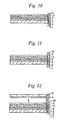
- Figs. 19 through 25 are simple cross sections depicting the method for manufacturing the organic EL display device in the present invention.
- a xylene solution of MEH-PPV was applied and dried in the form of a stripe by an ink jet head 20 to form a red-light emitting layer 21.
- a xylene solution of PPV was applied and dried in the form of a stripe by the ink jet head form a green light emitting layer 22 next to the above layer.
- a xylene solution of a fluorene compound was applied and dried in the form of a stripe by the ink jet head to form a blue light emitting layer 23 between the aforementioned MEH-PPV and PPV derivatives
- the resulting film was then placed in contact with a transparent glass substrate 8 having an aluminum and lithium alloy cathode 4 patterned with 256 stripes by laser, where the stripes of the light emitting layers were aligned with the stripes of the cathode ( Fig. 23 ).
- a pattern of 64 stripes was then produced with a YAG laser 7 on the film side so as to intersect the striped pattern of the cathode 2 ( Fig. 24 ).
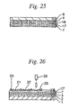
- the film was then removed, giving the organic EL substrate with 256 x 64 picture elements having the structure depicted in Fig. 25 .
- Embodiment 4 The same materials and manufacturing conditions given in Embodiment 4 can be used in this embodiment as well.
- This embodiment was carried out with the structure given in Embodiment 4, but it can similarly be applied in the preparation of the light emitting layers or electroluminescent adhesive layers in the other embodiments.
- This embodiment is an example of the formation of partition walls in the light emitting layer prior to the formation of the cathode on the film.
- partition walls 24 were printed in the widthwise direction between the colored light emitting layers by means of screen printing using thermosetting polyimide, and were heated and cured on the film used in Embodiment 5.
- An organic EL display device was then obtained in the same manner as in Embodiment 6.
- partition walls are not limited to those given here. Any other material and method capable of manufacturing the structure depicted in Fig. 26 can be used.
- ink may also be applied between picture elements following the formation of the electrode.
- the elemental structure can be the reverse of conventional structures, making it possible to suppress the loss of light that is caused by the effects of moving light when emitted light passes through a glass substrate.
- An organic EL display with high luminous efficiency can thus be inexpensively produced by a simple method.
Claims (8)
- Verfahren zur Herstellung einer organischen Elektrolumineszenzanzeige mit mindestens einer ersten Elektrode, einer zweiten Elektrode und einer Lichtemissionsschicht, die zwischen der ersten Elektrode und der zweite Elektrode bereitgestellt ist, wobei das Verfahren dadurch gekennzeichnet ist, dass es die folgenden Schritte umfasst:Bilden einer Licht/Wärme-Umwandlungsschicht und einer Wärmeausbreitungsschicht auf einem Film;Bilden der ersten Elektrode auf der Wärmeausbreitungsschicht;Auftragen eines Lichtemissionsmaterials, das in einem Lösemittel gelöst ist, auf die erste Elektrode zur Bildung der Lichtemissionsschicht;Anordnen des Films mit mehreren Schichten, einschließlich mindestens der ersten Elektrode und der darauf gebildeten Lichtemissionsschicht, in Kontakt mit einem Substrat, auf dem die zweite Elektrode gebildet ist, Bestrahlen der anderen Seite des Films mit einem Laser und anschließendes Übertragen der mehreren Schichten von dem Film auf das Substrat.
- Verfahren zur Herstellung einer organischen Elektrolumineszenzanzeige nach Anspruch 1, dadurch gekennzeichnet, dass die Lichtemissionsschicht eine Bindungsschicht zum Binden der ersten Elektrode und der mehreren Schichten ist.
- Verfahren zur Herstellung einer organischen Elektrolumineszenzanzeige nach Anspruch 1, dadurch gekennzeichnet, dass die erste Elektrode eine Kathode ist und die zweite Elektrode eine Anode ist.
- Verfahren zur Herstellung einer organischen Elektrolumineszenzanzeige nach Anspruch 3, dadurch gekennzeichnet, dass die mehreren Schichten des Weiteren eine positive Lochinjektionsschicht enthalten,
wobei die positive Lochinjektionsschicht eine Bindungsschicht zum Binden der Anode und der mehreren Schichten ist, und
die positive Lochinjektionsschicht zwischen der Lichtemissionsschicht und der Anode gebildet ist. - Verfahren zur Herstellung einer organischen Elektrolumineszenzanzeige nach Anspruch 1, dadurch gekennzeichnet, dass die erste Elektrode eine Anode ist und die zweite Elektrode eine Kathode ist.
- Verfahren zur Herstellung einer organischen Elektrolumineszenzanzeige nach Anspruch 5, dadurch gekennzeichnet, dass die mehreren Schichten des Weiteren eine positive Lochinjektionsschicht enthalten,
wobei die positive Lochinjektionsschicht eine Bindungsschicht zum Binden der Anodenschicht und der mehreren Schichten ist, und
die positive Lochinjektionsschicht zwischen der Lichtemissionsschicht und der Anode gebildet ist. - Verfahren zur Herstellung einer organischen Elektrolumineszenzanzeige nach einem der Ansprüche 1 bis 6, dadurch gekennzeichnet, dass die Lichtemissionsschicht auf der ersten Elektrode durch Auftragen lumineszenter Substanzen, die verschieden farbiges Licht emittieren, mit Hilfe eines Tintenstrahlkopfs gebildet wird.
- Verfahren zur Herstellung einer organischen Elektrolumineszenzanzeige nach Anspruch 7, dadurch gekennzeichnet, dass ein Mittel zur Tintentrennung zwischen Farbregionen vor dem Auftragen der lumineszenten Substanzen mit Hilfe eines Tintenstrahlkopfs bereitgestellt wird.
Applications Claiming Priority (2)
| Application Number | Priority Date | Filing Date | Title |
|---|---|---|---|
| JP05721498A JP4547723B2 (ja) | 1998-03-09 | 1998-03-09 | 有機el表示装置の製造方法 |
| EP99939247A EP1003354B1 (de) | 1998-03-09 | 1999-03-09 | Verfahren zur herstellung einer organischen elektrolumineszenzanzeige |
Related Parent Applications (1)
| Application Number | Title | Priority Date | Filing Date |
|---|---|---|---|
| EP99939247A Division EP1003354B1 (de) | 1998-03-09 | 1999-03-09 | Verfahren zur herstellung einer organischen elektrolumineszenzanzeige |
Publications (3)
| Publication Number | Publication Date |
|---|---|
| EP1624485A2 EP1624485A2 (de) | 2006-02-08 |
| EP1624485A3 EP1624485A3 (de) | 2006-11-29 |
| EP1624485B1 true EP1624485B1 (de) | 2008-05-21 |
Family
ID=13049286
Family Applications (2)
| Application Number | Title | Priority Date | Filing Date |
|---|---|---|---|
| EP05077308A Expired - Lifetime EP1624485B1 (de) | 1998-03-09 | 1999-03-09 | Verfahren zur Herstellung einer organischen Elektrolumineszenzanzeige |
| EP99939247A Expired - Lifetime EP1003354B1 (de) | 1998-03-09 | 1999-03-09 | Verfahren zur herstellung einer organischen elektrolumineszenzanzeige |
Family Applications After (1)
| Application Number | Title | Priority Date | Filing Date |
|---|---|---|---|
| EP99939247A Expired - Lifetime EP1003354B1 (de) | 1998-03-09 | 1999-03-09 | Verfahren zur herstellung einer organischen elektrolumineszenzanzeige |
Country Status (5)
| Country | Link |
|---|---|
| EP (2) | EP1624485B1 (de) |
| JP (1) | JP4547723B2 (de) |
| AT (1) | ATE314802T1 (de) |
| DE (2) | DE69929155T2 (de) |
| WO (1) | WO1999046961A1 (de) |
Cited By (1)
| Publication number | Priority date | Publication date | Assignee | Title |
|---|---|---|---|---|
| US9123595B2 (en) | 2001-12-28 | 2015-09-01 | Semiconductor Energy Laboratory Co., Ltd. | Method for fabricating a semiconductor device by bonding a layer to a support with curvature |
Families Citing this family (39)
| Publication number | Priority date | Publication date | Assignee | Title |
|---|---|---|---|---|
| US6165543A (en) * | 1998-06-17 | 2000-12-26 | Nec Corporation | Method of making organic EL device and organic EL transfer base plate |
| DE60035078T2 (de) | 1999-01-15 | 2008-01-31 | 3M Innovative Properties Co., St. Paul | Herstellungsverfahren eines Donorelements für Übertragung durch Wärme |
| US6114088A (en) | 1999-01-15 | 2000-09-05 | 3M Innovative Properties Company | Thermal transfer element for forming multilayer devices |
| JP4009923B2 (ja) | 1999-09-30 | 2007-11-21 | セイコーエプソン株式会社 | Elパネル |
| US6228555B1 (en) | 1999-12-28 | 2001-05-08 | 3M Innovative Properties Company | Thermal mass transfer donor element |
| US6284425B1 (en) | 1999-12-28 | 2001-09-04 | 3M Innovative Properties | Thermal transfer donor element having a heat management underlayer |
| US6436222B1 (en) * | 2000-05-12 | 2002-08-20 | Eastman Kodak Company | Forming preformed images in organic electroluminescent devices |
| JP2002083691A (ja) | 2000-09-06 | 2002-03-22 | Sharp Corp | アクティブマトリックス駆動型有機led表示装置及びその製造方法 |
| US6358664B1 (en) | 2000-09-15 | 2002-03-19 | 3M Innovative Properties Company | Electronically active primer layers for thermal patterning of materials for electronic devices |
| US6855384B1 (en) | 2000-09-15 | 2005-02-15 | 3M Innovative Properties Company | Selective thermal transfer of light emitting polymer blends |
| JP2002108250A (ja) | 2000-09-29 | 2002-04-10 | Sharp Corp | アクティブマトリックス駆動型自発光表示装置及びその製造方法 |
| JP2002190386A (ja) * | 2000-12-20 | 2002-07-05 | Daicel Chem Ind Ltd | 有機エレクトロルミネッセンス素子用材料およびその製造方法 |
| CN1401204A (zh) | 2000-12-20 | 2003-03-05 | 大赛璐化学工业株式会社 | 有机电致发光元件用的材料及其制造方法 |
| JP2002222694A (ja) | 2001-01-25 | 2002-08-09 | Sharp Corp | レーザー加工装置及びそれを用いた有機エレクトロルミネッセンス表示パネル |
| JP2002240437A (ja) | 2001-02-19 | 2002-08-28 | Sharp Corp | 薄膜形成用ドナーシートの製造方法、薄膜形成用ドナーシート及び有機エレクトロルミネッセンス素子 |
| US6767807B2 (en) | 2001-03-02 | 2004-07-27 | Fuji Photo Film Co., Ltd. | Method for producing organic thin film device and transfer material used therein |
| JP2002343564A (ja) | 2001-05-18 | 2002-11-29 | Sharp Corp | 転写用フィルムおよびそれを用いた有機エレクトロルミネッセンス素子の製造方法 |
| JP2002343565A (ja) | 2001-05-18 | 2002-11-29 | Sharp Corp | 有機led表示パネルの製造方法、その方法により製造された有機led表示パネル、並びに、その方法に用いられるベースフィルム及び基板 |
| MXPA04001412A (es) * | 2001-08-16 | 2004-07-15 | 3M Innovative Properties Co | Metodo y materiales para moldear matriz amorfa, polimerizable con material electricamente activo dispuesto en la misma. |
| US6699597B2 (en) | 2001-08-16 | 2004-03-02 | 3M Innovative Properties Company | Method and materials for patterning of an amorphous, non-polymeric, organic matrix with electrically active material disposed therein |
| TWI258317B (en) | 2002-01-25 | 2006-07-11 | Semiconductor Energy Lab | A display device and method for manufacturing thereof |
| US7241512B2 (en) | 2002-04-19 | 2007-07-10 | 3M Innovative Properties Company | Electroluminescent materials and methods of manufacture and use |
| GB0306409D0 (en) | 2003-03-20 | 2003-04-23 | Cambridge Display Tech Ltd | Electroluminescent device |
| JP2005032917A (ja) * | 2003-07-10 | 2005-02-03 | Dainippon Printing Co Ltd | 有機薄膜太陽電池の製造方法および転写シート |
| GB2412223B (en) * | 2004-03-20 | 2008-10-22 | Hewlett Packard Development Co | Method of applying light filters and busbars to a display substrate |
| JP4970242B2 (ja) * | 2004-03-20 | 2012-07-04 | ヒューレット−パッカード デベロップメント カンパニー エル.ピー. | ディスプレイ基材へのカラー素子及びバスバーの適用法 |
| JP4548153B2 (ja) * | 2005-03-07 | 2010-09-22 | セイコーエプソン株式会社 | 有機el表示装置の製造方法 |
| DE102006013834A1 (de) * | 2006-03-23 | 2007-09-27 | Tesa Ag | Elektrolumineszierende Haftklebemassen |
| US7670450B2 (en) | 2006-07-31 | 2010-03-02 | 3M Innovative Properties Company | Patterning and treatment methods for organic light emitting diode devices |
| JP4450006B2 (ja) | 2007-04-02 | 2010-04-14 | ソニー株式会社 | 転写用基板および有機電界発光素子の製造方法 |
| JP2009048811A (ja) | 2007-08-16 | 2009-03-05 | Sony Corp | 転写用基板および有機電界発光素子の製造方法 |
| US8080811B2 (en) | 2007-12-28 | 2011-12-20 | Semiconductor Energy Laboratory Co., Ltd. | Method for manufacturing evaporation donor substrate and light-emitting device |
| JP4502224B2 (ja) * | 2008-01-15 | 2010-07-14 | 大日本印刷株式会社 | パターン転写層を設けた有機el転写体、有機el被転写体および有機el素子の製造方法 |
| WO2009107548A1 (en) | 2008-02-29 | 2009-09-03 | Semiconductor Energy Laboratory Co., Ltd. | Deposition method and manufacturing method of light-emitting device |
| US8182863B2 (en) | 2008-03-17 | 2012-05-22 | Semiconductor Energy Laboratory Co., Ltd. | Deposition method and manufacturing method of light-emitting device |
| KR101629637B1 (ko) | 2008-05-29 | 2016-06-13 | 가부시키가이샤 한도오따이 에네루기 켄큐쇼 | 성막방법 및 발광장치의 제조방법 |
| CN104952702B (zh) * | 2015-05-15 | 2017-11-28 | 张家港康得新光电材料有限公司 | 半导体器件及其制作方法 |
| CN108878668A (zh) * | 2018-07-04 | 2018-11-23 | 京东方科技集团股份有限公司 | 背板及其制作方法、显示装置以及照明装置 |
| CN114055970A (zh) * | 2020-08-03 | 2022-02-18 | 湖南鼎一致远科技发展有限公司 | 可热转印的器件层结构和色带结构及其制备方法 |
Family Cites Families (14)
| Publication number | Priority date | Publication date | Assignee | Title |
|---|---|---|---|---|
| JPS61163591A (ja) * | 1985-01-11 | 1986-07-24 | 関西日本電気株式会社 | 有機型el素子の製造方法 |
| JPH06283265A (ja) * | 1993-03-25 | 1994-10-07 | Nec Kansai Ltd | 電界発光灯及びその製造方法及びその製造装置 |
| JPH0757871A (ja) * | 1993-08-19 | 1995-03-03 | Hitachi Ltd | 電場発光表示装置 |
| JP3585524B2 (ja) * | 1994-04-20 | 2004-11-04 | 大日本印刷株式会社 | 有機薄膜el素子の製造方法 |
| JPH07302685A (ja) * | 1994-05-10 | 1995-11-14 | Nec Kansai Ltd | 電界発光灯の製造方法 |
| US5563019A (en) * | 1994-06-30 | 1996-10-08 | E. I. Du Pont De Nemours And Company | Donor element for laser-induced thermal transfer |
| US5686383A (en) * | 1995-08-22 | 1997-11-11 | Eastman Kodak Company | Method of making a color filter array by colorant transfer and lamination |
| US5688551A (en) * | 1995-11-13 | 1997-11-18 | Eastman Kodak Company | Method of forming an organic electroluminescent display panel |
| US5766819A (en) * | 1995-11-29 | 1998-06-16 | E. I. Dupont De Nemours And Company | Donor elements, assemblages, and associated processes with flexible ejection layer(s) for laser-induced thermal transfer |
| US5695907A (en) * | 1996-03-14 | 1997-12-09 | Minnesota Mining And Manufacturing Company | Laser addressable thermal transfer imaging element and method |
| JP3036436B2 (ja) * | 1996-06-19 | 2000-04-24 | セイコーエプソン株式会社 | アクティブマトリックス型有機el表示体の製造方法 |
| US5998085A (en) * | 1996-07-23 | 1999-12-07 | 3M Innovative Properties | Process for preparing high resolution emissive arrays and corresponding articles |
| KR100195175B1 (ko) * | 1996-12-23 | 1999-06-15 | 손욱 | 유기전자발광소자 유기박막용 도너필름, 이를 이용한 유기전자발광소자의 제조방법 및 그 방법에 따라 제조된 유기전자발광소자 |
| JP3466876B2 (ja) * | 1997-06-16 | 2003-11-17 | キヤノン株式会社 | エレクトロ・ルミネセンス素子の製造法 |
-
1998
- 1998-03-09 JP JP05721498A patent/JP4547723B2/ja not_active Expired - Lifetime
-
1999
- 1999-03-09 DE DE69929155T patent/DE69929155T2/de not_active Expired - Lifetime
- 1999-03-09 EP EP05077308A patent/EP1624485B1/de not_active Expired - Lifetime
- 1999-03-09 AT AT99939247T patent/ATE314802T1/de not_active IP Right Cessation
- 1999-03-09 WO PCT/JP1999/001132 patent/WO1999046961A1/ja active IP Right Grant
- 1999-03-09 EP EP99939247A patent/EP1003354B1/de not_active Expired - Lifetime
- 1999-03-09 DE DE69938800T patent/DE69938800D1/de not_active Expired - Lifetime
Cited By (3)
| Publication number | Priority date | Publication date | Assignee | Title |
|---|---|---|---|---|
| US9123595B2 (en) | 2001-12-28 | 2015-09-01 | Semiconductor Energy Laboratory Co., Ltd. | Method for fabricating a semiconductor device by bonding a layer to a support with curvature |
| US9337341B2 (en) | 2001-12-28 | 2016-05-10 | Semiconductor Energy Laboratory Co., Ltd. | Semiconductor device having aluminum-containing layer between two curved substrates |
| US9536901B2 (en) | 2001-12-28 | 2017-01-03 | Semiconductor Energy Laboratory Co., Ltd. | Method for fabricating a semiconductor device by bonding a layer to a support with curvature |
Also Published As
| Publication number | Publication date |
|---|---|
| DE69938800D1 (de) | 2008-07-03 |
| EP1003354B1 (de) | 2005-12-28 |
| DE69929155D1 (de) | 2006-02-02 |
| DE69929155T2 (de) | 2006-08-24 |
| EP1624485A3 (de) | 2006-11-29 |
| EP1624485A2 (de) | 2006-02-08 |
| JPH11260549A (ja) | 1999-09-24 |
| WO1999046961A1 (fr) | 1999-09-16 |
| EP1003354A1 (de) | 2000-05-24 |
| ATE314802T1 (de) | 2006-01-15 |
| EP1003354A4 (de) | 2004-05-19 |
| JP4547723B2 (ja) | 2010-09-22 |
Similar Documents
| Publication | Publication Date | Title |
|---|---|---|
| EP1624485B1 (de) | Verfahren zur Herstellung einer organischen Elektrolumineszenzanzeige | |
| US6091196A (en) | Organic electroluminescent display device and method of manufacture thereof | |
| JP3861400B2 (ja) | 電界発光素子およびその製造方法 | |
| TW406520B (en) | Electro-luminescent device | |
| JP3902938B2 (ja) | 有機発光素子の製造方法及び有機発光表示体の製造方法、有機発光素子及び有機発光表示体 | |
| EP2238635B1 (de) | Hochleistungselektrolumineszenzvorrichtungen und herstellungsverfahren dafür | |
| KR100588440B1 (ko) | 유기 전계발광 소자 및 그의 제조 방법 | |
| US20020001026A1 (en) | Production of organic luminescence device | |
| JP2000208254A (ja) | 有機el素子の製造方法および有機el表示装置 | |
| JP2003264083A (ja) | 有機led素子とその製造方法 | |
| JPH10153967A (ja) | フルカラー有機el表示装置およびその製造方法 | |
| KR20110111429A (ko) | 표시 패널의 제조 방법 및 표시 장치용 기판 | |
| US20110175522A1 (en) | Substrate for patterned application and organic el element | |
| TW201332179A (zh) | 有機電激發光顯示面板及其製造方法 | |
| JP2000036391A (ja) | 有機電界発光素子およびその製造方法 | |
| JPH1187062A (ja) | 電界発光素子 | |
| JP4934649B2 (ja) | 有機エレクトロルミネッセンス素子の製造方法 | |
| JPH11345688A (ja) | 有機elディスプレイ | |
| JP3674848B2 (ja) | 有機薄膜発光ディスプレイ及びその製造方法 | |
| JP4548153B2 (ja) | 有機el表示装置の製造方法 | |
| US20050032453A1 (en) | Method for fabricating organic el element | |
| JP2001195012A (ja) | 有機エレクトロルミネッセンス表示装置およびその製造方法 | |
| US20110012102A1 (en) | Organic electroluminescence element, and method for production thereof | |
| WO2002087287A1 (fr) | Panneau electroluminescent, visualiseur d'image et procede permettant de les produire | |
| JP5292863B2 (ja) | 有機電界発光表示装置及びその製造方法 |
Legal Events
| Date | Code | Title | Description |
|---|---|---|---|
| PUAI | Public reference made under article 153(3) epc to a published international application that has entered the european phase |
Free format text: ORIGINAL CODE: 0009012 |
|
| 17P | Request for examination filed |
Effective date: 20051102 |
|
| AC | Divisional application: reference to earlier application |
Ref document number: 1003354 Country of ref document: EP Kind code of ref document: P |
|
| AK | Designated contracting states |
Kind code of ref document: A2 Designated state(s): AT BE CH CY DE DK ES FI FR GB GR IE IT LI LU MC NL PT SE |
|
| PUAL | Search report despatched |
Free format text: ORIGINAL CODE: 0009013 |
|
| AK | Designated contracting states |
Kind code of ref document: A3 Designated state(s): AT BE CH CY DE DK ES FI FR GB GR IE IT LI LU MC NL PT SE |
|
| RIC1 | Information provided on ipc code assigned before grant |
Ipc: H05B 33/10 20060101ALI20061026BHEP Ipc: H01L 51/40 20060101ALI20061026BHEP Ipc: H01L 27/00 20060101AFI20051115BHEP |
|
| AKX | Designation fees paid |
Designated state(s): CY DE DK ES FI FR GB |
|
| RBV | Designated contracting states (corrected) |
Designated state(s): AT BE CH CY DE DK ES FI FR GB LI |
|
| GRAP | Despatch of communication of intention to grant a patent |
Free format text: ORIGINAL CODE: EPIDOSNIGR1 |
|
| GRAS | Grant fee paid |
Free format text: ORIGINAL CODE: EPIDOSNIGR3 |
|
| GRAA | (expected) grant |
Free format text: ORIGINAL CODE: 0009210 |
|
| AC | Divisional application: reference to earlier application |
Ref document number: 1003354 Country of ref document: EP Kind code of ref document: P |
|
| AK | Designated contracting states |
Kind code of ref document: B1 Designated state(s): DE FR GB |
|
| REG | Reference to a national code |
Ref country code: GB Ref legal event code: FG4D |
|
| REF | Corresponds to: |
Ref document number: 69938800 Country of ref document: DE Date of ref document: 20080703 Kind code of ref document: P |
|
| PLBE | No opposition filed within time limit |
Free format text: ORIGINAL CODE: 0009261 |
|
| STAA | Information on the status of an ep patent application or granted ep patent |
Free format text: STATUS: NO OPPOSITION FILED WITHIN TIME LIMIT |
|
| 26N | No opposition filed |
Effective date: 20090224 |
|
| REG | Reference to a national code |
Ref country code: FR Ref legal event code: TQ Ref country code: FR Ref legal event code: CA Ref country code: FR Ref legal event code: CD |
|
| REG | Reference to a national code |
Ref country code: DE Ref legal event code: R081 Ref document number: 69938800 Country of ref document: DE Owner name: SEIKO EPSON CORP., JP Free format text: FORMER OWNER: SEIKO EPSON CORP., MINNESOTA MINING AND MANUFACTUR, , US Effective date: 20110505 Ref country code: DE Ref legal event code: R081 Ref document number: 69938800 Country of ref document: DE Owner name: 3M INNOVATIVE PROPERTIES CO., US Free format text: FORMER OWNER: SEIKO EPSON CORP., MINNESOTA MINING AND MANUFACTUR, , US Effective date: 20110505 Ref country code: DE Ref legal event code: R081 Ref document number: 69938800 Country of ref document: DE Owner name: 3M INNOVATIVE PROPERTIES CO., ST. PAUL, US Free format text: FORMER OWNER: SEIKO EPSON CORP., MINNESOTA MINING AND MANUFACTUR, , US Effective date: 20110505 Ref country code: DE Ref legal event code: R081 Ref document number: 69938800 Country of ref document: DE Owner name: 3M INNOVATIVE PROPERTIES CO., ST. PAUL, US Free format text: FORMER OWNERS: SEIKO EPSON CORP., TOKYO, JP; MINNESOTA MINING AND MANUFACTURING COMPANY, ST. PAUL, MINN., US Effective date: 20110505 Ref country code: DE Ref legal event code: R081 Ref document number: 69938800 Country of ref document: DE Owner name: SEIKO EPSON CORP., JP Free format text: FORMER OWNERS: SEIKO EPSON CORP., TOKYO, JP; MINNESOTA MINING AND MANUFACTURING COMPANY, ST. PAUL, MINN., US Effective date: 20110505 |
|
| REG | Reference to a national code |
Ref country code: FR Ref legal event code: PLFP Year of fee payment: 18 |
|
| REG | Reference to a national code |
Ref country code: FR Ref legal event code: PLFP Year of fee payment: 19 |
|
| REG | Reference to a national code |
Ref country code: FR Ref legal event code: PLFP Year of fee payment: 20 |
|
| PGFP | Annual fee paid to national office [announced via postgrant information from national office to epo] |
Ref country code: DE Payment date: 20180322 Year of fee payment: 20 Ref country code: GB Payment date: 20180307 Year of fee payment: 20 |
|
| PGFP | Annual fee paid to national office [announced via postgrant information from national office to epo] |
Ref country code: FR Payment date: 20180323 Year of fee payment: 20 |
|
| REG | Reference to a national code |
Ref country code: DE Ref legal event code: R071 Ref document number: 69938800 Country of ref document: DE |
|
| REG | Reference to a national code |
Ref country code: GB Ref legal event code: PE20 Expiry date: 20190308 |
|
| PG25 | Lapsed in a contracting state [announced via postgrant information from national office to epo] |
Ref country code: GB Free format text: LAPSE BECAUSE OF EXPIRATION OF PROTECTION Effective date: 20190308 |