EP1589585A1 - Halbleiterbauelement und dessen herstellungsverfahren - Google Patents
Halbleiterbauelement und dessen herstellungsverfahren Download PDFInfo
- Publication number
- EP1589585A1 EP1589585A1 EP03778874A EP03778874A EP1589585A1 EP 1589585 A1 EP1589585 A1 EP 1589585A1 EP 03778874 A EP03778874 A EP 03778874A EP 03778874 A EP03778874 A EP 03778874A EP 1589585 A1 EP1589585 A1 EP 1589585A1
- Authority
- EP
- European Patent Office
- Prior art keywords
- trench
- forming
- layer
- gate electrode
- region
- Prior art date
- Legal status (The legal status is an assumption and is not a legal conclusion. Google has not performed a legal analysis and makes no representation as to the accuracy of the status listed.)
- Withdrawn
Links
Images


Classifications
-
- H—ELECTRICITY
- H10—SEMICONDUCTOR DEVICES; ELECTRIC SOLID-STATE DEVICES NOT OTHERWISE PROVIDED FOR
- H10D—INORGANIC ELECTRIC SEMICONDUCTOR DEVICES
- H10D30/00—Field-effect transistors [FET]
- H10D30/60—Insulated-gate field-effect transistors [IGFET]
- H10D30/64—Double-diffused metal-oxide semiconductor [DMOS] FETs
- H10D30/66—Vertical DMOS [VDMOS] FETs
- H10D30/668—Vertical DMOS [VDMOS] FETs having trench gate electrodes, e.g. UMOS transistors
-
- H—ELECTRICITY
- H10—SEMICONDUCTOR DEVICES; ELECTRIC SOLID-STATE DEVICES NOT OTHERWISE PROVIDED FOR
- H10D—INORGANIC ELECTRIC SEMICONDUCTOR DEVICES
- H10D30/00—Field-effect transistors [FET]
- H10D30/01—Manufacture or treatment
- H10D30/021—Manufacture or treatment of FETs having insulated gates [IGFET]
- H10D30/028—Manufacture or treatment of FETs having insulated gates [IGFET] of double-diffused metal oxide semiconductor [DMOS] FETs
- H10D30/0291—Manufacture or treatment of FETs having insulated gates [IGFET] of double-diffused metal oxide semiconductor [DMOS] FETs of vertical DMOS [VDMOS] FETs
- H10D30/0297—Manufacture or treatment of FETs having insulated gates [IGFET] of double-diffused metal oxide semiconductor [DMOS] FETs of vertical DMOS [VDMOS] FETs using recessing of the gate electrodes, e.g. to form trench gate electrodes
-
- H—ELECTRICITY
- H10—SEMICONDUCTOR DEVICES; ELECTRIC SOLID-STATE DEVICES NOT OTHERWISE PROVIDED FOR
- H10D—INORGANIC ELECTRIC SEMICONDUCTOR DEVICES
- H10D64/00—Electrodes of devices having potential barriers
- H10D64/111—Field plates
- H10D64/112—Field plates comprising multiple field plate segments
-
- H—ELECTRICITY
- H10—SEMICONDUCTOR DEVICES; ELECTRIC SOLID-STATE DEVICES NOT OTHERWISE PROVIDED FOR
- H10D—INORGANIC ELECTRIC SEMICONDUCTOR DEVICES
- H10D64/00—Electrodes of devices having potential barriers
- H10D64/111—Field plates
- H10D64/117—Recessed field plates, e.g. trench field plates or buried field plates
-
- H—ELECTRICITY
- H10—SEMICONDUCTOR DEVICES; ELECTRIC SOLID-STATE DEVICES NOT OTHERWISE PROVIDED FOR
- H10D—INORGANIC ELECTRIC SEMICONDUCTOR DEVICES
- H10D64/00—Electrodes of devices having potential barriers
- H10D64/20—Electrodes characterised by their shapes, relative sizes or dispositions
- H10D64/27—Electrodes not carrying the current to be rectified, amplified, oscillated or switched, e.g. gates
- H10D64/311—Gate electrodes for field-effect devices
- H10D64/411—Gate electrodes for field-effect devices for FETs
- H10D64/511—Gate electrodes for field-effect devices for FETs for IGFETs
- H10D64/512—Disposition of the gate electrodes, e.g. buried gates
- H10D64/513—Disposition of the gate electrodes, e.g. buried gates within recesses in the substrate, e.g. trench gates, groove gates or buried gates
-
- H—ELECTRICITY
- H10—SEMICONDUCTOR DEVICES; ELECTRIC SOLID-STATE DEVICES NOT OTHERWISE PROVIDED FOR
- H10D—INORGANIC ELECTRIC SEMICONDUCTOR DEVICES
- H10D64/00—Electrodes of devices having potential barriers
- H10D64/20—Electrodes characterised by their shapes, relative sizes or dispositions
- H10D64/27—Electrodes not carrying the current to be rectified, amplified, oscillated or switched, e.g. gates
- H10D64/311—Gate electrodes for field-effect devices
- H10D64/411—Gate electrodes for field-effect devices for FETs
- H10D64/511—Gate electrodes for field-effect devices for FETs for IGFETs
- H10D64/514—Gate electrodes for field-effect devices for FETs for IGFETs characterised by the insulating layers
- H10D64/516—Gate electrodes for field-effect devices for FETs for IGFETs characterised by the insulating layers the thicknesses being non-uniform
-
- H—ELECTRICITY
- H10—SEMICONDUCTOR DEVICES; ELECTRIC SOLID-STATE DEVICES NOT OTHERWISE PROVIDED FOR
- H10D—INORGANIC ELECTRIC SEMICONDUCTOR DEVICES
- H10D64/00—Electrodes of devices having potential barriers
- H10D64/20—Electrodes characterised by their shapes, relative sizes or dispositions
- H10D64/27—Electrodes not carrying the current to be rectified, amplified, oscillated or switched, e.g. gates
- H10D64/311—Gate electrodes for field-effect devices
- H10D64/411—Gate electrodes for field-effect devices for FETs
- H10D64/511—Gate electrodes for field-effect devices for FETs for IGFETs
- H10D64/517—Gate electrodes for field-effect devices for FETs for IGFETs characterised by the conducting layers
- H10D64/518—Gate electrodes for field-effect devices for FETs for IGFETs characterised by the conducting layers characterised by their lengths or sectional shapes
Definitions
- the present invention relates to a semiconductor device having a trench structure and a manufacturing method thereof and, in particular, to a high-frequency switching MOSFET having a trench structure and a manufacturing method thereof.
- Fig. 5 is a schematic sectional view showing the structure of a semiconductor device provided with a MOSFET having a conventional trench structure.
- N - epitaxial layer 52 Formed on the surface of a silicon substrate 51 is an N - epitaxial layer 52, and formed on the N - epitaxial layer 52 is a diffusion region 65.
- a plurality of trenches 54 are formed at a uniform interval so as to penetrate through the diffusion region 65 to the middle of the N - epitaxial layer 52 in the thickness direction thereof.
- a gate electrode 55 made of polysilicon which is made conductive by introduction of an impurity is arranged inside the trench 54.
- a gate oxide film 56 is provided along the inner wall of the trench 54. That is, the gate electrode 55 is opposed to the N - epitaxial layer 52 and the diffusion region 65 with the gate oxide film 56 interposed therebetween.
- the inner side wall of the trench 54 is formed as a substantially flat face and the bottom of the trench 54 constitutes a curved face projected to the silicon substrate 51 side.
- the interface between the gate oxide film 56 and the diffusion region 65 and between the gate oxide film 56 and N - epitaxial layer 52 has a flat face 56f and a curved face 56c.
- the flat face 56f is formed along a face at the diffusion region 65, which face has a specific plane direction to give a low resistance when electric current flows along the face.
- An N + source region 57 is formed at the periphery (rim) of the trench 54 in a surface layer portion of the diffusion region 65.
- the rest of the diffusion region 65 constitutes a channel region 53 of a P-conductivity type.
- An insulating film 59 made of silicon oxide is formed so as to cover an upper part of the trench 54.
- the insulating film 59 also exists at the rim of the trench 54 (on the N + source region 57) in a plan view.
- a contact hole 60 is formed between two adjacent insulating films 59.
- An electrode film 61 made of metal such as aluminum is provided on the diffusion region 65 and the insulating film 59. The electrode film 61 is formed so as to fill the contact hole 60.
- drain current flows across the N + source region 57 and the N - epitaxial layer 52.
- the drain current flows near the gate oxide film 56 in the channel region 53, along the gate oxide film 56.
- Such a semiconductor device is disclosed in, for example, Japanese Unexamined Patent Publication No. 8-167711 (1966).
- a semiconductor device constructed as described above cannot be used suitably for high-frequency switching (a DC-DC converter, for example). Although low ON resistance and low switching loss are required for a semiconductor device to be used for such purpose, a semiconductor device constructed as described above cannot strike a balance between reduction of ON resistance and reduction of switching loss. This is for the following reason.
- Drain current which flows near the gate oxide film 56 along the gate oxide film 56, is to flow along the curved face 56c when the current comes near the curved face 56c, in a state where the channel region 53 is in contact with the curved face 5 6c. Therefore, since the path of the drain current includes a path which deviates from a face having a plane direction to give a low resistance, the ON resistance is increased. Accordingly, in order to decrease the ON resistance, the channel region 53 needs to be in contact only with the flat face 56f of the gate oxide film 56 as shown in Fig. 5. That is, the curved face 56c is made contact with the N - epitaxial layer 52 by the whole area.
- a semiconductor device constructed as described above has difficulty in operating satisfactorily by a frequency of 1 MHz, though the device can operate and be used by a frequency of 300 kHz, for example.
- An object of the present invention is to provide a semiconductor device capable of reducing the ON resistance while reducing the switching loss.
- Another object of the present invention is to provide a manufacturing method of a semiconductor device capable of reducing the ON resistance while reducing the switching loss.
- the present invention relates to a semiconductor device comprising: a channel region of a first conductivity type formed at a surface layer portion of a semiconductor substrate; a source region of a second conductivity type which is different from the first conductivity type, the source region being formed at a rim of a trench having a depth sufficient to penetrate through the channel region; a drain region of the second conductivity type formed at a region adjacent to a bottom of the trench; a gate insulating film formed along an inner side wall of the trench; a gate electrode arranged in the trench so as to be opposed to the channel region with the gate insulating film interposed therebetween; a conductive layer formed in the trench so as to be nearer to the drain region than the gate electrode; and an insulating layer surrounding the conductive layer to electrically insulate the conductive layer from the gate electrode and the drain region.
- this semiconductor device functions as a MOSFET (Metal-Oxide-Semiconductor Field Effect Transistor).
- An insulating film, a conductive layer (including a semiconductor layer which is made conductive: the same applies to the following description) and an insulating film are arranged in this order between the gate electrode and the drain region. Accordingly, a portion extending from the gate electrode to the drain region is equivalent to a plurality of capacitors connected in series.
- a conductive layer for example, it can be considered that two capacitors are connected in series between the gate electrode and the drain region. Since the combination capacity of a plurality of capacitors connected in series is smaller than the capacity of each capacitor, the capacity between the gate electrode and the drain region is reduced.
- a plurality of conductive layers may be formed with the insulating layers also formed between the plurality of conductive layers.
- a portion extending from the gate electrode to the drain region is equivalent to three or more capacitors connected in series and the capacity between the gate electrode and the drain region is further reduced.
- the inner side wall of the trench may be formed into a substantially flat face and this flat face may be a face in the channel region, the face having a specific plane direction to give a low resistance when electric current flows along the face.
- this flat face may be a face in the channel region, the face having a specific plane direction to give a low resistance when electric current flows along the face.
- the drain current can flow only along the face having a plane direction to give a low resistance, it is possible to decrease the ON resistance. Moreover, even when the gate electrode is opposed to the drain region by a large area along this curved face, it is possible to decrease the switching loss of this semiconductor device since the capacity therebetween is small.
- An epitaxial layer may be formed on the surface of the semiconductor substrate and, in this case, the channel region, the source region and the drain region may be formed in the epitaxial layer.
- a portion of the insulating layer, the portion existing between the conductive layer and the drain region, and the gate insulating film may be made of silicon oxide, for example, obtained by oxidizing the inner side wall of this trench.
- the conductive layer may be made of polysilicon which is made conductive by introduction of an impurity.
- Polysilicon which is made conductive by introduction of an impurity is commonly performed in manufacturing processes of a semiconductor device. Accordingly, it is needless to use a special device for formation of such a conductive layer made of polysilicon.
- Polysilicon which is made conductive can be obtained by, for example, forming a polysilicon film by CVD (Chemical Vapor Deposition) and then performing ion implantation of an impurity for this polysilicon film.
- a portion of the insulating film, the portion existing between the conductive layer and the gate electrode, may be made of oxide silicon obtained by oxidizing a portion of the conductive layer.
- a manufacturing method of a semiconductor device of the present invention is a manufacturing method of a semiconductor device comprising: a channel region of a first conductivity type formed at a surface layer portion of a semiconductor substrate; a source region of a second conductivity type which is different from the first conductivity type, the source region being formed at a rim of a trench having a depth sufficient to penetrate through the channel region; a drain region of the second conductivity type formed at a region adjacent to a bottom of the trench; a gate insulating film formed along an inner side wall of the trench; a gate electrode arranged in the trench so as to be opposed to the channel region with the gate insulating film interposed therebetween; a conductive layer formed in the trench so as to be nearer to the drain region than the gate electrode; and an insulating layer surrounding the conductive layer to electrically insulate the conductive layer from the gate electrode and the drain region.
- This method includes: a step of forming an epitaxial layer of the second conductivity type at a surface layer portion of a semiconductor substrate; a step of forming the trench at this epitaxial layer; a step of forming a first insulating layer at a bottom of the trench; a step of forming the conductive layer on the first insulating layer in the trench after the step of forming this first insulating layer; a step of forming a second insulating layer at an exposed surface of this conductive layer after the step of forming this conductive layer, the second insulating layer composing the insulating layer together with the first insulating layer; a step of forming the gate insulating film along the inner side wall of the trench; a step of forming the gate electrode in the trench, the gate electrode being electrically insulated from the conductive layer by the insulating layer; a step of forming the channel region of the first conductivity type at the epitaxial layer, the channel region being to be opposed to the gate electrode with the gate insulating film interposed there
- the drain region may be the rest of the epitaxial layer after the channel region and the source region are formed, for example.
- the step of forming the channel region and the step of forming the source region may be implemented before the step of forming the trench or after the step of forming the trench.
- the step of forming the first insulating layer may include a step of forming a sacrificial oxide film by performing thermal oxidation for an inner wall of the trench and a step of removing the sacrificial oxide film with a portion thereof existing at a bottom of the trench being left and, in this case, the step of forming the second insulating layer may include a step of oxidizing an exposed surface of the conductive layer.
- the other portion of the insulating layer may be formed by oxidizing the exposed surface of the conductive layer. When forming the gate insulating film by thermal oxidation, the exposed surface of the conductive layer can be oxidized simultaneously.
- the step of forming the gate electrode may include a step of forming a polysilicon film which is made conductive by introduction of an impurity.
- Fig. 1 is a schematic sectional view showing the structure of a semiconductor device 20 according to an embodiment of the present invention.
- the semiconductor device 20 is a high-frequency switching MOSFET.
- N - epitaxial layer 2 Formed on the surface of a silicon substrate 1 is an N - epitaxial layer 2, and formed on the N - epitaxial layer 2 is a diffusion region 30.
- a plurality of trenches 17 are formed at a uniform interval so as to penetrate through the diffusion region 30 to the middle of the N - epitaxial layer 2 in the thickness direction thereof.
- the respective trenches 17 extend substantially parallel to each other in a direction vertical to the paper surface of Fig. 1.
- the inner side wall of the trench 17 is formed as a substantially flat face and the bottom of the trench 17 is formed as a curved face projected to the silicon substrate 1 side.
- a conductive layer 40 and a gate electrode 26 made of polysilicon which is made conductive by introduction of an impurity are arranged inside the trench 17.
- the conductive layer 40 is arranged at a region of a deep portion (N - epitaxial layer 2 side) of the trench 17, which region is opposed to the N - epitaxial layer 2 and the diffusion region 30.
- the gate electrode 26 is arranged separately from the conductive layer 40 at a portion shallower than the conductive layer 40 in the trench 17. Moreover, the gate electrode 26 is interposed between the diffusion region 30 and the conductive layer 40 at a deep portion of the trench 17.
- a gate oxide film 13 is formed at a region extending along the inner wall of the trench 17.
- the gate electrode 26 is opposed to the diffusion region 30 with the gate oxide film 13 interposed therebetween.
- the conductive layer 40 is surrounded by an oxide layer 15. Accordingly, the oxide layer 15 exists between the conductive layer 40 and the gate electrode 26 and between the conductive layer 40 and the N - epitaxial layer 2. As a result, the conductive layer 40 is electrically insulated from the gate electrode 26 and the N - epitaxial layer 2.
- the gate electrode 26 is electrically insulated from the N - epitaxial layer 2 by the gate oxide film 13 and the oxide layer 15.
- the gate oxide film 13 and the oxide layer 15 compose an integrated oxide film 18.
- the interface between the gate oxide film 13 and the diffusion region 30 is formed into a substantially flat face 13f as a reflection of the shape of the trench 17.
- the flat face 13f is formed along a face at a channel region 4, which face has a specific plane direction to give a low resistance when electric current flows along the face.
- the specific plane direction is (1, 0, 0), for example.
- the interface between the oxide layer 15 and the N - epitaxial layer 2 has a curved face 15c projected to the silicon substrate 1 side as a reflection of the shape of the trench 17.
- the diffusion region 30 is in contact only with the flat face 13f of the oxide film 18 and is not in contact with the curved face 15c.
- N + source region 25 is formed at a surface layer portion of the diffusion region 30 and the rest of the diffusion region 30 constitutes the P-type channel region 4.
- the N + source region 25 is formed at the periphery (rim) of the trench 17.
- an insulating film 28 made of oxide silicon Formed on the gate electrode 26 is an insulating film 28 made of oxide silicon.
- the insulating film 28 extends to the rim of the trench 17 (on the N + source region 25) in a plan view.
- Acontact hole 31 is formedbetween two adjacent insulating films 28.
- An electrode film 27 made of metal such as aluminum is provided on the diffusion region 30 and the insulating film 28. The electrode film 27 is formed so as to fill the contact hole 31 and is in contact with the diffusion region 30 exposed in the contact hole 31.
- drain current flows across the N + source region 25 and the N - epitaxial layer 2 when appropriate voltage is applied between the N + source region 25 and the N - epitaxial layer 2 to maintain the gate electrode 26 at an electric potential higher than or equal to a certain level. That is, the N - epitaxial layer 2 functions as a drain region.
- the drain current flows in the channel region 4 along the gate oxide film 13.
- the drain current flows along the flat face 13f of the gate oxide film 13 and does not flow along the curved face 15c. Accordingly, since the drain current can flow in the channel region 4 along the face having the specific plane direction to give a low resistance, the ON resistance is low.
- the ON resistance of such a semiconductor device 20 can be 5 m ⁇ to 7 m ⁇ or lower, for example.
- the oxide layer 15, the conductive layer 40 and the oxide layer 15 are arranged in this order between the gate electrode 26 and the N - epitaxial layer 2. Accordingly, a portion extending from the gate electrode 26 to the N - epitaxial layer 2 is equivalent to two capacitors connected in series. The combination capacity of two capacitors connected in series is smaller than the capacity of each capacitor. Therefore, even though the gate electrode 26 is opposed to the N - epitaxial layer 2 by a large area via the curved face 15c, the capacity between the gate electrode 26 and the N - epitaxial layer 2, i.e. a drain-gate capacitor C DG , is reduced. Accordingly, the switching loss of such a semiconductor device 20 is low.
- the power conversion efficiency (ratio of output power to input power) of a case of driving the CPU by 1.3V can be approximately 85% and the power conversion efficiency of a case of driving the CPU by 3.3V or 5V can be approximately 90%.
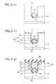
- Fig. 2 (a) to Fig. 2 (g) are schematic sectional views for explaining a manufacturing method of the semiconductor device 20 shown in Fig. 1.
- the N - epitaxial layer 2 is formed on the surface of the silicon substrate 1.
- the trench 17 having a predetermined depth is formed by reactive ion etching (RIE).
- RIE reactive ion etching
- the bottom of the trench 17 is formed as a curved face projected to the silicon substrate 1 side. This state is shown in Fig. 2(a).
- the exposed surface of the semiconductor substrate 1 which has undergone the above processes i.e. the inner wall of the trench 17 and the surface of the N - epitaxial layer 2, undergoes thermal oxidation, so that a sacrificial oxide film 11 is formed.
- the thickness of the sacrificial oxide film 11 is, for example, approximately 1500 ⁇ to 3000 ⁇ (approximately 2000 ⁇ , for example). This state is shown in Fig. 2(b).
- a polysilicon film 12 is formed on the silicon substrate 1, which has undergone the above processes, by CVD (Chemical Vapor Deposition) so as to fill the inside of the trench 17 (see Fig. 2(c)). Then, an impurity is introduced into the polysilicon film 12 to make the polysilicon film 12 conductive. Furthermore, the polysilicon film 12 undergoes etching back with a portion existing at the bottom of the trench 17 (portion of the silicon substrate 1 side) being left (see Fig. 2(d)).
- the sacrificial oxide film 11 undergoes etching back.
- a portion of the side wall of the polysilicon film 12 is exposed so that the sacrificial oxide film 11 (portion at the bottom side of the trench 17) between the N - epitaxial layer 2 and the polysilicon film 12 is left.
- the width of the trench 17 at a portion from which the sacrificial oxide film 11 has been removed is slightly larger. Moreover, the inner wall of the trench 17 from which the sacrificial oxide film 11 has been removed is formed into a substantially flat face. This state is shown in Fig. 2(e).
- the exposed surface of the silicon substrate 1 which has undergone the above processes undergoes thermal oxidation.
- the gate oxide film 13 is formed at the inner side wall of the trench 17 and an oxide film 14 is formed on the exposed surface of the polysilicon film 12.
- the thickness of the gate oxide film 13 is, for example, 200 ⁇ to 600 ⁇ .
- the rest of the polysilicon film 12 constitutes the conductive layer 40.
- the rest of the sacrificial oxide film 11 and the oxide film 14 compose the oxide layer 15 surrounding the conductive layer 40 and the oxide layer 15 and the gate oxide film 13 compose the integrated oxide film 18.
- the interface between the gate oxide film 13 and the diffusion region 30 is formed into the substantially flat face 13f as a reflection of the shape of the trench 17.
- the interface between the oxide layer 15 and the N - epitaxial layer 2 has the curved face 15c as a reflection of the shape of the trench 17. This state is shown in Fig. 2(f).
- a polysilicon film is formed by CVD so as to fill the inside of the trench 17 and an impurity is introduced into this polysilicon film to make the film conductive. A portion of this polysilicon film existing outside the trench 17 is then removed. The rest of the polysilicon film constitutes the gate electrode 26.
- ion implantation is performed for the N epitaxial layer 2 with a mask having an aperture of a predetermined pattern to form the P-type channel region 4. Furthermore, ion implantation is performed for the channel region 4 with a mask having an aperture of another pattern to form the N + source region 25.
- the channel region 4 and the N + source region 25 compose the diffusion region 30.
- the depth of ion implantation is controlled so that the diffusion region 30 comes in contact only with the flat face 13f of the oxide film 18 and not with the curved face 15c. Moreover, the diffusion region 30 is opposed to the gate electrode 26 by the whole area with the gate oxide film 13 interposed therebetween.
- the insulating film 28 made of oxide silicon is then formed on the whole area of the silicon substrate 1, which has undergone the above processes, by CVD (see Fig. 2(g)).
- the contact hole 31 is then formed at the insulating film 28 using a mask having an aperture of a predetermined pattern.
- the electrode film 27 made of aluminum or the like is formed on the whole area of the silicon substrate 1, which has undergone the above processes, to obtain the semiconductor device 20 shown in Fig. 1.
- this sacrificial oxide film 11 is not removed completely but a part thereof existing between the polysilicon film 12 and the N - epitaxial layer 2 is left. Accordingly, the oxide layer 15 can be formed without increasing the processes significantly.
- the thickness of the oxide layer 15 existing between the conductive layer 40 and the N - epitaxial layer 2 can be increased. With this modification, it is also possible to reduce the capacity between the gate electrode 26 and the N - epitaxial layer 2 and to reduce the switching loss.
- Fig. 3 is a schematic sectional view showing the structure of a semiconductor device 21 according to another embodiment of the present invention. Like reference symbols are used to refer to parts corresponding to the respective parts of the semiconductor device 20 shown in Fig. 1 and explanation thereof is omitted.
- a gate electrode 36 and a conductive layer 37 are provided corresponding respectively to the gate electrode 26 and the conductive layer 40 of the semiconductor device 20 shown in Fig. 1.
- a portion of the gate electrode 26 in the semiconductor device 20 is interposed between the N - epitaxial layer 2 and the conductive layer 40 while the gate electrode 36 in this semiconductor device 21 is not interposed between the N - epitaxial layer 2 and the conductive layer 37.
- the gate electrode 36 and the conductive layer 37 are compartmentalized by the substantially flat oxide layer 15.
- Such a semiconductor device 21 can be obtained by preventing the sacrificial oxide film 11 between the N - epitaxial layer 2 and the polysilicon film 12 from being removed in the step of removing the sacrificial oxide film 11 in the manufacturing method of the semiconductor device 20 (see Fig. 2(e)). That is, it is only necessary to stop etching back of the sacrificial oxide film 11 when the etched back face of the polysilicon film 12 (face opposite to the silicon substrate 1 side) and the etching back face of the sacrificial oxide film 11 form substantially the same face.
- Fig. 4 is a schematic sectional view showing the structure of a semiconductor device 22 according to yet another embodiment of the present invention. Like reference symbols are used to refer to parts corresponding to the respective parts of the semiconductor device 20 shown in Fig. 1 and explanation thereof is omitted.
- Only one conductive layer 40 is formed in the semiconductor device 20 shown in Fig. 1 while two conductive layers 40a and 40b are formed in this semiconductor device 22.
- the conductive layers 40a and 40b are arranged along the depth direction of the trench 17 and the oxide layer 15 also exists between the conductive layer 40a and the conductive layer 40b.
- the oxide layer 15, the conductive layer 40a, the oxide layer 15, the conductive layer 40b and the oxide layer 15 are arranged in this order between the gate electrode 26 and the N - epitaxial layer 2.
- a portion extending from the gate electrode 26 to the N - epitaxial layer 2 is equivalent to three capacitors connected in series and it is possible to further reduce the capacity between the gate electrode 26 and the N - epitaxial layer 2.
- the semiconductor device 22 it is possible with the semiconductor device 22 to further reduce the switching loss in comparison with the semiconductor devices 20 and 21.
- Three or more conductive layers may be provided instead of the conductive layers 40, 40a and 40b.
- Such a semiconductor device 22 can be obtained as described hereinafter.
- the processes up to formation of the gate oxide film 13 by thermal oxidation are implemented similarly as the manufacturing method of the semiconductor device 20.
- a polysilicon film similar to the polysilicon film 12 is formed in the trench 17, an impurity is introduced into this polysilicon film to make the film conductive and then this polysilicon film undergoes etching back.
- the rest of the polysilicon film constitutes the conductive layer 40a.
- the exposed surface of the conductive layer 40a undergoes thermal oxidation, then a polysilicon film similar to the polysilicon film 12 is formed, an impurity is introduced into this polysilicon film to make the film conductive and then, furthermore, a portion of this polysilicon film existing outside the trench 17 undergoes etching back.
- the rest of the polysilicon film constitutes the gate electrode 26.
- the gate electrode 26 and the conductive layers 40, 40a and 40b may be made of metal such as tungsten (W).
- the channel region 4 and the N + source region 25 are formedbefore forming the trench 17 in the above embodiments, they may be formed after forming the trench 17.
- a semiconductor device may be a P-channel transistor.
Landscapes
- Electrodes Of Semiconductors (AREA)
- Insulated Gate Type Field-Effect Transistor (AREA)
Applications Claiming Priority (3)
| Application Number | Priority Date | Filing Date | Title |
|---|---|---|---|
| JP2003019066 | 2003-01-28 | ||
| JP2003019066A JP4202149B2 (ja) | 2003-01-28 | 2003-01-28 | 半導体装置およびその製造方法 |
| PCT/JP2003/015947 WO2004068587A1 (ja) | 2003-01-28 | 2003-12-12 | 半導体装置およびその製造方法 |
Publications (2)
| Publication Number | Publication Date |
|---|---|
| EP1589585A1 true EP1589585A1 (de) | 2005-10-26 |
| EP1589585A4 EP1589585A4 (de) | 2010-06-23 |
Family
ID=32820601
Family Applications (1)
| Application Number | Title | Priority Date | Filing Date |
|---|---|---|---|
| EP03778874A Withdrawn EP1589585A4 (de) | 2003-01-28 | 2003-12-12 | Halbleiterbauelement und dessen herstellungsverfahren |
Country Status (7)
| Country | Link |
|---|---|
| US (1) | US7288815B2 (de) |
| EP (1) | EP1589585A4 (de) |
| JP (1) | JP4202149B2 (de) |
| KR (1) | KR20050089888A (de) |
| CN (1) | CN100573911C (de) |
| TW (1) | TWI306313B (de) |
| WO (1) | WO2004068587A1 (de) |
Cited By (2)
| Publication number | Priority date | Publication date | Assignee | Title |
|---|---|---|---|---|
| DE102006026943A1 (de) * | 2006-06-09 | 2007-12-13 | Infineon Technologies Austria Ag | Mittels Feldeffekt steuerbarer Trench-Transistor mit zwei Steuerelektroden |
| DE102007004323A1 (de) * | 2007-01-29 | 2008-07-31 | Infineon Technologies Austria Ag | Bauelementanordnung mit einem eine Feldelektrode aufweisenden MOS-Transistor |
Families Citing this family (16)
| Publication number | Priority date | Publication date | Assignee | Title |
|---|---|---|---|---|
| JP5259920B2 (ja) * | 2004-08-04 | 2013-08-07 | ローム株式会社 | 半導体装置およびその製造方法 |
| DE102004057237B4 (de) * | 2004-11-26 | 2007-02-08 | Infineon Technologies Ag | Verfahren zum Herstellen von Kontaktlöchern in einem Halbleiterkörper sowie Transistor mit vertikalem Aufbau |
| JP4971595B2 (ja) * | 2005-03-15 | 2012-07-11 | ルネサスエレクトロニクス株式会社 | 半導体装置 |
| JP4955222B2 (ja) * | 2005-05-20 | 2012-06-20 | ルネサスエレクトロニクス株式会社 | 半導体装置の製造方法 |
| AT504290A2 (de) | 2005-06-10 | 2008-04-15 | Fairchild Semiconductor | Feldeffekttransistor mit ladungsgleichgewicht |
| TWI400757B (zh) | 2005-06-29 | 2013-07-01 | 快捷半導體公司 | 形成遮蔽閘極場效應電晶體之方法 |
| JP4817827B2 (ja) * | 2005-12-09 | 2011-11-16 | 株式会社東芝 | 半導体装置 |
| US7521773B2 (en) * | 2006-03-31 | 2009-04-21 | Fairchild Semiconductor Corporation | Power device with improved edge termination |
| JP5183959B2 (ja) * | 2007-04-23 | 2013-04-17 | 新日本無線株式会社 | Mosfet型半導体装置の製造方法 |
| JP5266738B2 (ja) * | 2007-12-05 | 2013-08-21 | トヨタ自動車株式会社 | トレンチゲート型半導体装置の製造方法 |
| JP5195357B2 (ja) * | 2008-12-01 | 2013-05-08 | トヨタ自動車株式会社 | 半導体装置 |
| DE102011079747A1 (de) | 2010-07-27 | 2012-02-02 | Denso Corporation | Halbleitervorrichtung mit Schaltelement und Freilaufdiode, sowie Steuerverfahren hierfür |
| JP5374575B2 (ja) * | 2011-12-26 | 2013-12-25 | ルネサスエレクトロニクス株式会社 | 半導体装置の製造方法 |
| CN103247529B (zh) * | 2012-02-10 | 2016-08-03 | 无锡华润上华半导体有限公司 | 一种沟槽场效应器件及其制作方法 |
| JP6600475B2 (ja) * | 2015-03-27 | 2019-10-30 | ローム株式会社 | 半導体装置 |
| CN119153539A (zh) * | 2024-11-18 | 2024-12-17 | 珠海格力电子元器件有限公司 | 半导体结构以及半导体器件 |
Family Cites Families (15)
| Publication number | Priority date | Publication date | Assignee | Title |
|---|---|---|---|---|
| JPS613458A (ja) * | 1984-06-15 | 1986-01-09 | Nec Corp | Misトランジスタ |
| JPS63245954A (ja) * | 1987-04-01 | 1988-10-13 | Hitachi Ltd | 半導体メモリ |
| JP2507502B2 (ja) * | 1987-12-28 | 1996-06-12 | 三菱電機株式会社 | 半導体装置 |
| US5283201A (en) * | 1988-05-17 | 1994-02-01 | Advanced Power Technology, Inc. | High density power device fabrication process |
| KR950006483B1 (ko) * | 1990-06-13 | 1995-06-15 | 가부시끼가이샤 도시바 | 종형 mos트랜지스터와 그 제조방법 |
| JP3361922B2 (ja) * | 1994-09-13 | 2003-01-07 | 株式会社東芝 | 半導体装置 |
| US5998833A (en) * | 1998-10-26 | 1999-12-07 | North Carolina State University | Power semiconductor devices having improved high frequency switching and breakdown characteristics |
| JP3773755B2 (ja) * | 2000-06-02 | 2006-05-10 | セイコーインスツル株式会社 | 縦形mosトランジスタ及びその製造方法 |
| EP1170803A3 (de) * | 2000-06-08 | 2002-10-09 | Siliconix Incorporated | MOSFET mit Graben-Gateelektrode und Verfahren zu dessen Herstellung |
| JP4528460B2 (ja) | 2000-06-30 | 2010-08-18 | 株式会社東芝 | 半導体素子 |
| US6309929B1 (en) * | 2000-09-22 | 2001-10-30 | Industrial Technology Research Institute And Genetal Semiconductor Of Taiwan, Ltd. | Method of forming trench MOS device and termination structure |
| JP4797265B2 (ja) * | 2001-03-21 | 2011-10-19 | 富士電機株式会社 | 半導体装置および半導体装置の製造方法 |
| JP4009825B2 (ja) | 2002-02-20 | 2007-11-21 | サンケン電気株式会社 | 絶縁ゲート型トランジスタ |
| CN100514672C (zh) * | 2002-08-23 | 2009-07-15 | 快捷半导体有限公司 | 用于改进mos栅控从而降低米勒电容和开关损失的方法和装置 |
| US6759702B2 (en) * | 2002-09-30 | 2004-07-06 | International Business Machines Corporation | Memory cell with vertical transistor and trench capacitor with reduced burried strap |
-
2003
- 2003-01-28 JP JP2003019066A patent/JP4202149B2/ja not_active Expired - Lifetime
- 2003-12-12 KR KR1020057013724A patent/KR20050089888A/ko not_active Ceased
- 2003-12-12 US US10/543,533 patent/US7288815B2/en not_active Expired - Lifetime
- 2003-12-12 WO PCT/JP2003/015947 patent/WO2004068587A1/ja not_active Ceased
- 2003-12-12 EP EP03778874A patent/EP1589585A4/de not_active Withdrawn
- 2003-12-12 CN CNB2003801092424A patent/CN100573911C/zh not_active Expired - Lifetime
- 2003-12-17 TW TW092135699A patent/TWI306313B/zh not_active IP Right Cessation
Cited By (5)
| Publication number | Priority date | Publication date | Assignee | Title |
|---|---|---|---|---|
| DE102006026943A1 (de) * | 2006-06-09 | 2007-12-13 | Infineon Technologies Austria Ag | Mittels Feldeffekt steuerbarer Trench-Transistor mit zwei Steuerelektroden |
| DE102006026943B4 (de) * | 2006-06-09 | 2011-01-05 | Infineon Technologies Austria Ag | Mittels Feldeffekt steuerbarer Trench-Transistor mit zwei Steuerelektroden |
| US8093655B2 (en) | 2006-06-09 | 2012-01-10 | Infineon Technologies Austria Ag | Integrated circuit including a trench transistor having two control electrodes |
| DE102007004323A1 (de) * | 2007-01-29 | 2008-07-31 | Infineon Technologies Austria Ag | Bauelementanordnung mit einem eine Feldelektrode aufweisenden MOS-Transistor |
| US8405146B2 (en) | 2007-01-29 | 2013-03-26 | Infineon Technologies Austria Ag | Component arrangement including a MOS transistor having a field electrode |
Also Published As
| Publication number | Publication date |
|---|---|
| WO2004068587A1 (ja) | 2004-08-12 |
| JP2004235231A (ja) | 2004-08-19 |
| TW200417043A (en) | 2004-09-01 |
| CN1742378A (zh) | 2006-03-01 |
| EP1589585A4 (de) | 2010-06-23 |
| US20060199319A1 (en) | 2006-09-07 |
| JP4202149B2 (ja) | 2008-12-24 |
| KR20050089888A (ko) | 2005-09-08 |
| CN100573911C (zh) | 2009-12-23 |
| TWI306313B (en) | 2009-02-11 |
| US7288815B2 (en) | 2007-10-30 |
Similar Documents
| Publication | Publication Date | Title |
|---|---|---|
| US7288815B2 (en) | Semiconductor device and manufacturing method thereof | |
| KR100766874B1 (ko) | 트렌치 dmos를 형성하는 방법과, 이러한 dmos 트랜지스터 셀과, 이러한 트랜지스터 구조 | |
| US7319256B1 (en) | Shielded gate trench FET with the shield and gate electrodes being connected together | |
| JP4860821B2 (ja) | 半導体デバイス製造方法 | |
| US7935992B2 (en) | Transistor, display driver integrated circuit including a transistor, and a method of fabricating a transistor | |
| US9722071B1 (en) | Trench power transistor | |
| US7646062B2 (en) | Semiconductor device comprising buried wiring layer | |
| JPH01192174A (ja) | 半導体装置の製造方法 | |
| JP2005150475A (ja) | 半導体装置およびその製造方法 | |
| KR20060111859A (ko) | 스크리닝 전극을 가진 반도체 장치 및 방법 | |
| US9679963B2 (en) | Semiconductor structure and a method for processing a carrier | |
| US6624470B2 (en) | Semiconductor device and a method for manufacturing same | |
| US9954099B1 (en) | Transistor structure | |
| US20130292765A1 (en) | Semiconductor device having a drain-gate isolation portion | |
| JP2006108208A (ja) | Ldmosトランジスタを含む半導体装置 | |
| US11742420B2 (en) | Semiconductor device and structure therefor | |
| US6884684B2 (en) | High density trench power MOSFET structure and fabrication method thereof | |
| CN108962972B (zh) | 沟槽式功率半导体元件及其制造方法 | |
| EP2105962A2 (de) | Halbleiterbauelement und Herstellungsverfahren dafür | |
| JP3632565B2 (ja) | 半導体装置の製造方法 | |
| US20150115357A1 (en) | Semiconductor device | |
| JPH0620134B2 (ja) | 半導体装置 | |
| HK1081327B (en) | Lateral insulated gate fet structure with improved on resistance performance | |
| HK1081327A1 (en) | Lateral insulated gate fet structure with improved on resistance performance | |
| JPH05190843A (ja) | 半導体装置 |
Legal Events
| Date | Code | Title | Description |
|---|---|---|---|
| PUAI | Public reference made under article 153(3) epc to a published international application that has entered the european phase |
Free format text: ORIGINAL CODE: 0009012 |
|
| 17P | Request for examination filed |
Effective date: 20050729 |
|
| AK | Designated contracting states |
Kind code of ref document: A1 Designated state(s): AT BE BG CH CY CZ DE DK EE ES FI FR GB GR HU IE IT LI LU MC NL PT RO SE SI SK TR |
|
| RBV | Designated contracting states (corrected) |
Designated state(s): DE FR GB NL |
|
| A4 | Supplementary search report drawn up and despatched |
Effective date: 20100525 |
|
| RIC1 | Information provided on ipc code assigned before grant |
Ipc: H01L 29/78 20060101ALI20100518BHEP Ipc: H01L 29/40 20060101AFI20100518BHEP Ipc: H01L 21/336 20060101ALI20100518BHEP |
|
| 17Q | First examination report despatched |
Effective date: 20110114 |
|
| STAA | Information on the status of an ep patent application or granted ep patent |
Free format text: STATUS: THE APPLICATION IS DEEMED TO BE WITHDRAWN |
|
| 18D | Application deemed to be withdrawn |
Effective date: 20121205 |