EP1582892B1 - Optical component - Google Patents
Optical component Download PDFInfo
- Publication number
- EP1582892B1 EP1582892B1 EP05011306A EP05011306A EP1582892B1 EP 1582892 B1 EP1582892 B1 EP 1582892B1 EP 05011306 A EP05011306 A EP 05011306A EP 05011306 A EP05011306 A EP 05011306A EP 1582892 B1 EP1582892 B1 EP 1582892B1
- Authority
- EP
- European Patent Office
- Prior art keywords
- optical member
- optical
- base member
- top surface
- substrate
- Prior art date
- Legal status (The legal status is an assumption and is not a legal conclusion. Google has not performed a legal analysis and makes no representation as to the accuracy of the status listed.)
- Expired - Lifetime
Links
- 230000003287 optical effect Effects 0.000 title claims description 251
- 239000000758 substrate Substances 0.000 claims description 106
- 239000011347 resin Substances 0.000 claims description 27
- 229920005989 resin Polymers 0.000 claims description 27
- 239000000463 material Substances 0.000 claims description 20
- 239000003566 sealing material Substances 0.000 claims description 8
- 230000001154 acute effect Effects 0.000 claims description 7
- 229920001187 thermosetting polymer Polymers 0.000 claims description 5
- 238000003384 imaging method Methods 0.000 claims description 2
- 238000000034 method Methods 0.000 description 71
- 238000004519 manufacturing process Methods 0.000 description 50
- 239000002243 precursor Substances 0.000 description 45
- 239000011344 liquid material Substances 0.000 description 21
- 238000001723 curing Methods 0.000 description 18
- 230000008569 process Effects 0.000 description 15
- 230000000694 effects Effects 0.000 description 7
- 239000011521 glass Substances 0.000 description 7
- 238000000059 patterning Methods 0.000 description 6
- 229920001721 polyimide Polymers 0.000 description 5
- 230000004048 modification Effects 0.000 description 4
- 238000012986 modification Methods 0.000 description 4
- 239000009719 polyimide resin Substances 0.000 description 4
- 238000005488 sandblasting Methods 0.000 description 4
- 238000001039 wet etching Methods 0.000 description 4
- 239000000470 constituent Substances 0.000 description 3
- 238000005530 etching Methods 0.000 description 3
- 238000010438 heat treatment Methods 0.000 description 3
- 238000009736 wetting Methods 0.000 description 3
- XKRFYHLGVUSROY-UHFFFAOYSA-N Argon Chemical compound [Ar] XKRFYHLGVUSROY-UHFFFAOYSA-N 0.000 description 2
- KRHYYFGTRYWZRS-UHFFFAOYSA-N Fluorane Chemical compound F KRHYYFGTRYWZRS-UHFFFAOYSA-N 0.000 description 2
- 239000000853 adhesive Substances 0.000 description 2
- 230000001070 adhesive effect Effects 0.000 description 2
- 230000001419 dependent effect Effects 0.000 description 2
- 239000003822 epoxy resin Substances 0.000 description 2
- 239000007789 gas Substances 0.000 description 2
- 239000002245 particle Substances 0.000 description 2
- 238000000206 photolithography Methods 0.000 description 2
- 229920000647 polyepoxide Polymers 0.000 description 2
- HMUNWXXNJPVALC-UHFFFAOYSA-N 1-[4-[2-(2,3-dihydro-1H-inden-2-ylamino)pyrimidin-5-yl]piperazin-1-yl]-2-(2,4,6,7-tetrahydrotriazolo[4,5-c]pyridin-5-yl)ethanone Chemical compound C1C(CC2=CC=CC=C12)NC1=NC=C(C=N1)N1CCN(CC1)C(CN1CC2=C(CC1)NN=N2)=O HMUNWXXNJPVALC-UHFFFAOYSA-N 0.000 description 1
- VZSRBBMJRBPUNF-UHFFFAOYSA-N 2-(2,3-dihydro-1H-inden-2-ylamino)-N-[3-oxo-3-(2,4,6,7-tetrahydrotriazolo[4,5-c]pyridin-5-yl)propyl]pyrimidine-5-carboxamide Chemical compound C1C(CC2=CC=CC=C12)NC1=NC=C(C=N1)C(=O)NCCC(N1CC2=C(CC1)NN=N2)=O VZSRBBMJRBPUNF-UHFFFAOYSA-N 0.000 description 1
- WZFUQSJFWNHZHM-UHFFFAOYSA-N 2-[4-[2-(2,3-dihydro-1H-inden-2-ylamino)pyrimidin-5-yl]piperazin-1-yl]-1-(2,4,6,7-tetrahydrotriazolo[4,5-c]pyridin-5-yl)ethanone Chemical compound C1C(CC2=CC=CC=C12)NC1=NC=C(C=N1)N1CCN(CC1)CC(=O)N1CC2=C(CC1)NN=N2 WZFUQSJFWNHZHM-UHFFFAOYSA-N 0.000 description 1
- 239000004925 Acrylic resin Substances 0.000 description 1
- 229920000178 Acrylic resin Polymers 0.000 description 1
- IJGRMHOSHXDMSA-UHFFFAOYSA-N Atomic nitrogen Chemical compound N#N IJGRMHOSHXDMSA-UHFFFAOYSA-N 0.000 description 1
- 229910001218 Gallium arsenide Inorganic materials 0.000 description 1
- 239000004642 Polyimide Substances 0.000 description 1
- XUIMIQQOPSSXEZ-UHFFFAOYSA-N Silicon Chemical compound [Si] XUIMIQQOPSSXEZ-UHFFFAOYSA-N 0.000 description 1
- 239000002390 adhesive tape Substances 0.000 description 1
- 239000012670 alkaline solution Substances 0.000 description 1
- 229910052786 argon Inorganic materials 0.000 description 1
- 238000005422 blasting Methods 0.000 description 1
- 230000008859 change Effects 0.000 description 1
- 230000008878 coupling Effects 0.000 description 1
- 238000010168 coupling process Methods 0.000 description 1
- 238000005859 coupling reaction Methods 0.000 description 1
- 229910001873 dinitrogen Inorganic materials 0.000 description 1
- 238000001312 dry etching Methods 0.000 description 1
- 239000011261 inert gas Substances 0.000 description 1
- 238000007641 inkjet printing Methods 0.000 description 1
- 238000010884 ion-beam technique Methods 0.000 description 1
- 230000001678 irradiating effect Effects 0.000 description 1
- 239000007788 liquid Substances 0.000 description 1
- 239000004973 liquid crystal related substance Substances 0.000 description 1
- 239000013307 optical fiber Substances 0.000 description 1
- 230000009290 primary effect Effects 0.000 description 1
- 239000004065 semiconductor Substances 0.000 description 1
- 229910052710 silicon Inorganic materials 0.000 description 1
- 239000010703 silicon Substances 0.000 description 1
- 238000005507 spraying Methods 0.000 description 1
Images


Classifications
-
- G—PHYSICS
- G02—OPTICS
- G02B—OPTICAL ELEMENTS, SYSTEMS OR APPARATUS
- G02B7/00—Mountings, adjusting means, or light-tight connections, for optical elements
- G02B7/02—Mountings, adjusting means, or light-tight connections, for optical elements for lenses
- G02B7/025—Mountings, adjusting means, or light-tight connections, for optical elements for lenses using glue
-
- H—ELECTRICITY
- H10—SEMICONDUCTOR DEVICES; ELECTRIC SOLID-STATE DEVICES NOT OTHERWISE PROVIDED FOR
- H10F—INORGANIC SEMICONDUCTOR DEVICES SENSITIVE TO INFRARED RADIATION, LIGHT, ELECTROMAGNETIC RADIATION OF SHORTER WAVELENGTH OR CORPUSCULAR RADIATION
- H10F99/00—Subject matter not provided for in other groups of this subclass
-
- B—PERFORMING OPERATIONS; TRANSPORTING
- B29—WORKING OF PLASTICS; WORKING OF SUBSTANCES IN A PLASTIC STATE IN GENERAL
- B29D—PRODUCING PARTICULAR ARTICLES FROM PLASTICS OR FROM SUBSTANCES IN A PLASTIC STATE
- B29D11/00—Producing optical elements, e.g. lenses or prisms
- B29D11/00009—Production of simple or compound lenses
- B29D11/00278—Lenticular sheets
-
- B—PERFORMING OPERATIONS; TRANSPORTING
- B29—WORKING OF PLASTICS; WORKING OF SUBSTANCES IN A PLASTIC STATE IN GENERAL
- B29D—PRODUCING PARTICULAR ARTICLES FROM PLASTICS OR FROM SUBSTANCES IN A PLASTIC STATE
- B29D11/00—Producing optical elements, e.g. lenses or prisms
- B29D11/00009—Production of simple or compound lenses
- B29D11/00365—Production of microlenses
-
- B—PERFORMING OPERATIONS; TRANSPORTING
- B41—PRINTING; LINING MACHINES; TYPEWRITERS; STAMPS
- B41J—TYPEWRITERS; SELECTIVE PRINTING MECHANISMS, i.e. MECHANISMS PRINTING OTHERWISE THAN FROM A FORME; CORRECTION OF TYPOGRAPHICAL ERRORS
- B41J2/00—Typewriters or selective printing mechanisms characterised by the printing or marking process for which they are designed
- B41J2/005—Typewriters or selective printing mechanisms characterised by the printing or marking process for which they are designed characterised by bringing liquid or particles selectively into contact with a printing material
- B41J2/01—Ink jet
-
- G—PHYSICS
- G02—OPTICS
- G02B—OPTICAL ELEMENTS, SYSTEMS OR APPARATUS
- G02B3/00—Simple or compound lenses
- G02B3/0006—Arrays
- G02B3/0012—Arrays characterised by the manufacturing method
-
- G—PHYSICS
- G02—OPTICS
- G02B—OPTICAL ELEMENTS, SYSTEMS OR APPARATUS
- G02B3/00—Simple or compound lenses
- G02B3/0006—Arrays
- G02B3/0037—Arrays characterized by the distribution or form of lenses
- G02B3/0056—Arrays characterized by the distribution or form of lenses arranged along two different directions in a plane, e.g. honeycomb arrangement of lenses
-
- G—PHYSICS
- G02—OPTICS
- G02B—OPTICAL ELEMENTS, SYSTEMS OR APPARATUS
- G02B7/00—Mountings, adjusting means, or light-tight connections, for optical elements
- G02B7/02—Mountings, adjusting means, or light-tight connections, for optical elements for lenses
- G02B7/027—Mountings, adjusting means, or light-tight connections, for optical elements for lenses the lens being in the form of a sphere or ball
-
- H—ELECTRICITY
- H01—ELECTRIC ELEMENTS
- H01L—SEMICONDUCTOR DEVICES NOT COVERED BY CLASS H10
- H01L23/00—Details of semiconductor or other solid state devices
-
- B—PERFORMING OPERATIONS; TRANSPORTING
- B41—PRINTING; LINING MACHINES; TYPEWRITERS; STAMPS
- B41J—TYPEWRITERS; SELECTIVE PRINTING MECHANISMS, i.e. MECHANISMS PRINTING OTHERWISE THAN FROM A FORME; CORRECTION OF TYPOGRAPHICAL ERRORS
- B41J2202/00—Embodiments of or processes related to ink-jet or thermal heads
- B41J2202/01—Embodiments of or processes related to ink-jet heads
- B41J2202/09—Ink jet technology used for manufacturing optical filters
-
- G—PHYSICS
- G02—OPTICS
- G02B—OPTICAL ELEMENTS, SYSTEMS OR APPARATUS
- G02B3/00—Simple or compound lenses
- G02B3/0006—Arrays
- G02B3/0075—Arrays characterized by non-optical structures, e.g. having integrated holding or alignment means
Definitions
- the present invention relates to an microlens structure whose siting, shape and size are well controlled.
- an optical member such as a lens
- a droplet of a liquid material is ejected onto a substrate and then cured.
- this method it is difficult to obtain an optical member having a properly adjusted focal length, because the shape of the optical member that is formed is constrained by the contact angle between the droplet and the substrate.
- a method according to the pre-characterizing portion of claim 1 is known from HAYES D J ET AL: "Ink-jet printing in the manufacture of electronics, photonics, and displays", Nanoscale Optics and Applications, Seattle, WA, USA, 8-9 July 2002, vol. 4809, pages 94-99 , XP002269974 .
- the diameter of the base member determines the diameter of the optical member formed thereon.
- the purpose of the present invention is to provide an microlens structure whose siting, shape and size are well controlled and to provide a method of manufacturing such an microlens structure.
- the optical member By embedding the perimeter of the optical member using a sealing material the optical member can be reliably secured to the top surface of the base member.
- the microlens structure of the present invention comprises a base member disposed upon a substrate, and an optical member disposed upon the top surface of the base member.
- substrate refers to an object having a surface upon which the base member can be formed.
- the surface may be flat or may be curved, as long as the base member can be formed thereupon. Therefore, as long as it has such a surface, the shape of the substrate itself is not specifically prescribed.
- the base member may also be formed so that it is integrated with the substrate.
- base member refers to a member having a top surface upon which the optical member can be formed
- top surface of the base member refers to the surface upon which the optical member is formed.
- the top surface of the base member may be flat or may be curved, as long as the optical member can be formed thereupon.
- optical member refers to a member having a function that changes the character or travel direction of light.
- the present invention by controlling the shape, height and other characteristics of the top surface of the base member by using the aforementioned configuration, it is possible to obtain an microlens structure that includes an optical member whose siting, shape and size are well-controlled. Details will be provided in the description of the preferred embodiment.
- microlens structure of the present invention can take any of the forms described below in (1) through (10).
- the upper part of the base member may form an inverse tapered shape.
- the upper part of the base member refers to the region in the vicinity of the top surface of the base member.
- a method of manufacturing an microlens structure of the present invention comprises:
- the present invention by controlling the shape, height, siting and other characteristics of the top surface of the base member in the step of (a), and by, for example, controlling the volume of the ejected droplet in the step of (b), it is possible to form an microlens structure containing an optical member whose siting, shape and size are well controlled. Details will be provided in the
- the method of manufacturing an microlens structure of the present invention can take any of the forms described below in (1) - (7).
- a method of manufacturing an microlens structure according to the present invention comprises:
- the optical member is used as a discrete microlens structure, and thus the optical member can be removed from the top surface of the base member by a simple and convenient method.
- the base member in the step of (a) may be formed with a material that transmits light of a prescribed wavelength.
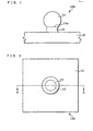
- FIG. 1 is a sectional view that schematically shows an optical component 100.
- FIG. 2 is a plan view that schematically shows the optical component 100 shown in FIG. 1.
- FIG. 1 is a cross-sectional view at line A - A in FIG. 2.
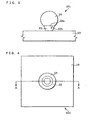
- FIG. 3, FIG. 5 and FIG. 7 are sectional views that schematically show a modification example wherein the shape of a base member 12 of the optical component 100 shown in FIG. 1 is changed.
- FIG. 4, FIG. 6, and FIG. 8 are plan views that schematically show optical components 101, 102, and 103 shown in FIG. 3, FIG. 5 and FIG. 7, respectively.
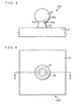
- FIG. 11 is a sectional view that schematically shows a modification example wherein the shape of the base member 12 and an optical member 14 of the optical component 100 shown in FIG. 1 is changed.
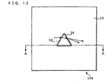
- FIG. 12 is a plan view that schematically shows the optical component 104 shown in FIG. 11.
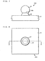
- FIG. 27 is a sectional view that schematically shows a modification example wherein the shape of the base member 12 and the optical member 14 of the optical component 100 shown in FIG. 1 is changed.
- FIG. 28 is a plan view that schematically shows an optical component 105 shown in FIG. 27.
- the optical component 100 comprises the base member 12 disposed on a substrate 10, and an optical member disposed on a top surface 12a of the base member 12.
- the optical member 14 may have, for example, one or more of functions like condensing, polarizing or separating rays of incident light. The constituent elements of the optical component are explained below, with reference primarily to FIG. 1 and FIG. 2.
- the substrate 10 may be, for example, a semiconductor substrate such as a silicon substrate or a GaAs substrate, or a glass substrate.
- the base member 12 consists of a material that transmits light of a prescribed wavelength.
- the base member 12 includes a material that can transmit incident light to the optical member 14.
- the base member 12 may be formed using a polyimide resin, an acrylic resin, an epoxy resin or a fluorinated resin.
- the present embodiment refers to a case in which the base member 12 consists of a material that transmits light of a prescribed wavelength, but the base member 12 may also be formed from a material that absorbs light of a prescribed wavelength.
- the base member 12 may also be formed so that it is integrated with the substrate 10.
- the base member 12 in this case is formed from the same material as the substrate 10.
- This type of the base member 12 can be formed, for example, by patterning the substrate 10.
- Modification examples (the optical components 101, 102, 103) in which the three-dimensional shape of the base member 12 shown in FIG. 1 and FIG. 2 was changed are shown in FIG. 3 through FIG. 8.
- the three-dimensional shape of the base member is not particularly prescribed, but at a minimum the structure must be such that an optical member can be disposed thereupon.
- the base member 12 of the optical component 100 is such that the top surface 12a can support the optical member 14 thereupon.
- the angle ⁇ formed between a top surface 22a and a side surface 22b of a base member 22 can be made an acute angle.
- the side surface 22b of the base member 22 refers to the surface within the side member of the base member 22 that is adjacent to the top surface 22a.
- the side member of base member 22 is the side surface 22b of the base member 22.
- the optical member 14 is formed by first ejecting a droplet onto the top surface 22a of the base member 22 so as to form an optical member precursor (to be explained later), and by then curing the optical member precursor. Therefore, the acute angle ⁇ formed between the top surface 22a and the side surface 22b of the base member 22 prevents the side surface 22b of the base member 22 from becoming wet by the droplet when a droplet is ejected to the top surface 22a of the base member 22. As a result, it is possible to reliably form an optical member 14 having the desired shape and size. For example, as shown in FIG. 3 and 4, the cross section of optical member 14 is formed greater than the cross section of base member 22.
- the three-dimensional shape of the base member 32 can be formed such that the upper part 32c of the base member 32 forms an inverse tapered shape.
- an acute angle ⁇ is formed between a top surface 32a of a base member 32 and the side surface 32b of it (the surface within the side member of the base member 32 that is adjacent to the top surface 32a).
- the angle ⁇ formed between the top surface 32a and side surface 32a of the base member 32 can be made smaller while maintaining the stability of the base member 32.
- the side surface 32b of the base member 32 can be reliably prevented from becoming wet by the droplet. As a result, it is possible to more reliably form the optical member 14 having the desired shape and size.
- the shape of the top surface of the base member is determined by such considerations as the function and application of the optical member formed on the top surface of the base member. In other words, the shape of the optical member can be controlled by controlling the shape of the top surface of the base member.
- the top surface 12a of the base member 12 is round.
- the top surface of the base member is also depicted as being round.
- the top surface of the base member is made round. This enables the optical member to be formed in a three-dimensional spherical shape or in a sectioned spherical shape, and the optical member thus obtained can be used as a lens or as a polarizing element.
- An example in which the optical member 14 of the optical component 100 shown in FIG. 1 and FIG. 2 is applied as a lens is shown in FIG. 9. In other words, as shown in FIG. 9, light rays can be gathered and condensed by the optical member (lens) 14.
- the optical member 14 of the optical component 100 shown in FIG. 1 and FIG. 2 is applied as a polarizing element is shown in FIG. 10. In other words, as shown in FIG. 10, the travel direction of the light can be changed by the optical member (polarizing element) 14.
- the optical member is used as an anisotropic lens or as a polarizing element, for example, then the top surface of the base member is made elliptical. This enables the optical member to be formed in a three-dimensional elliptical spherical shape or in a sectioned elliptical spherical shape, and the optical member thus obtained can be used as an anisotropic lens or as a polarizing element.
- the top surface of the base member may be made triangular.
- This optical member whose base member has a triangular shape, is formed by ejecting a droplet on to the top surface of the base member so as to form an optical member precursor, and by then curing the optical member precursor.
- the optical member thus formed can be used as a light-splitting element.
- FIG. 11 is a cross-sectional view at line A - A in FIG. 12.
- a base member 52 is triangular. Therefore, the shape of a top surface 52a of the base member 52 is triangular.
- the optical member 24 functions as a light-splitter (prism). Specifically, as shown in FIG. 12, the light incident on an optical member 24 is split upon exit.
- top surface is depicted as comprising a plane.
- a top surface 62a of a base member 62 may also be a curved surface.
- an essentially spherical optical member 34 may be disposed on the top surface 62a of the base member 62.
- the optical member has a three-dimensional shape that depends on the optical member's application and function. Details regarding the three-dimensional shape of the optical member will be omitted here, as they were provided in conjunction with the explanation regarding the base member.
- the optical member 14 is formed, for example, by curing a liquid material that can be cured by applying heat or light or some other form of energy.
- the optical member 14 in the present embodiment is formed by first ejecting a droplet consisting of the aforementioned liquid material to the top surface 12a of the base member 12 so as to form an optical member precursor (to be explained later), and by then curing the optical member precursor.
- thermosetting resin A precursor of an ultraviolet curing resin or of a thermosetting resin, for example, can be cited as the aforementioned liquid material.
- An ultraviolet curing resin and epoxy resin can be cited as examples of an ultraviolet curing resin.
- a thermosetting polyimide resin can be exemplified as a thermosetting resin.
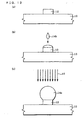
- FIG. 13(a) to FIG. 13(c) are sectional views that schematically show the process for manufacturing the optical component 100 shown in FIG. 1 and FIG. 2, respectively.
- the base member 12 is formed on the substrate 10 [FIG. 13(a)].
- the base member 12 can be formed by selecting a suitable method (for example, a selective growth method, a dry etching method, a wet etching method, a lift-off method, a transfer method, etc.) according to the material, shape, and size of the base member 12.
- the optical member 14 is formed [FIG. 13(b)]. Specifically, a droplet 14b of a liquid material for forming the optical member 14 is ejected on to the top surface 12a of the base member 12 so as to form an optical member precursor 14a. As described above, the liquid material is such that it can be cured by the application of energy 15.
- a dispenser method or an inkjet method can be cited as methods for ejecting the droplet 14b.
- a dispenser method is commonly used to eject droplets and is effective when ejecting the droplet 14b over a relatively large area.
- droplets are ejected using an inkjet head, with micron-order control possible over the location in which droplets are ejected.
- an optical member of a minute structure can be produced.
- a lyophilic process or a lyophobic process is performed so that the wettability of the top surface 12a with respect to the droplet 14b can be controlled.
- a lyophilic process or a lyophobic process is performed so that the wettability of the top surface 12a with respect to the droplet 14b can be controlled.
- the optical member precursor 14a is cured so as to form the optical member 14 [FIG. 13(c)]. Specifically, heat or light or some other form of energy is applied to the optical member precursor 14a.
- a suitable method of curing the optical member precursor 14a is used according to the type of liquid material used. Specifically, the application of thermal energy, or the irradiation with ultraviolet light or laser light can be cited as examples of curing methods. The aforesaid process is used to obtain the optical component 100 that includes an optical member (FIG. 1 and FIG. 2).
- the optical member 14 can also be removed from the optical component 100 that is formed and can be used as a discrete optical component.
- the optical member 14 can be removed by spraying a gas 16 (an inert gas such as argon gas or nitrogen gas, for example) on the interface between the base member 12 and the optical member 14.
- a gas 16 an inert gas such as argon gas or nitrogen gas, for example
- the optical member 14 can be removed from the top surface 12a of the base member 12 by affixing adhesive tape (not shown) to the top of the optical member 14 and then pulling off the tape.
- optical component and the method of manufacturing the optical component of the present embodiment has the effect shown below.
- FIG. 29 is a sectional view that schematically shows the area around the interface between the base member 12 and the optical member precursor 14c, in the manufacturing process (FIG. 13(a) to FIG. 13(c)) for the optical component 100 described above. Specifically, FIG. 29 is an enlarged view of the cross section in FIG. 13(c).
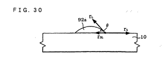
- FIG. 30 is a sectional view that schematically shows the method for manufacturing a commonly used optical component.
- One known method for manufacturing an optical member involves first ejecting a liquid material onto the substrate 10 to form an optical member precursor, and then curing the optical member precursor to obtain an optical member.
- FIG. 30 is a sectional view showing a liquid material for forming the optical member after the liquid material has been ejected onto the substrate 10. Specifically, FIG. 30 shows the state before the optical member precursor is cured; that is, the state in which the optical member precursor 92a, which is composed of the liquid material, is situated on top of the substrate 10.
- the curvature of an optical member precursor 92a made up of the liquid material is limited by the contact angle ⁇ determined by Formula (1).
- the curvature of the optical member obtained after the optical member precursor 92a has been cured is primarily dependent on the material of the substrate 10 and of the liquid material.
- the curvature of the optical member is one factor that determines the shape of the optical member. Consequently, it is difficult to control the shape of the optical member that is formed using this manufacturing method.
- a method is known wherein a film for adjusting the wetting angle is first formed in a prescribed location on the surface of the substrate 10, after which a droplet of a liquid material is ejected, thereby increasing the contact angle ⁇ of the liquid material.
- the shape of the optical member can be controlled to some extent.
- the optical member precursor 14a is formed on the top surface 12a of the base member 12, as shown in FIG. 29. Accordingly, as long as the side surface 12b of the base member 12 is not wetted by the optical member precursor 14a, the surface tension of the base member 12 does not affect the optical member precursor 14a. Instead, it is the surface tension ⁇ L of the optical member precursor 14a that has the primary effect. For this reason, the shape of the optical member precursor 14a can be controlled by adjusting the volume of the droplet used to form the optical member precursor 14a. As a result, it is possible to obtain the optical member 14 having the desired shape and size.
- Example 1 provides an example wherein the optical component 100 is applied to a micro lens substrate.
- the micro lens substrate is disposed, for example, in a pixel member of a liquid crystal display panel, in a receiver surface of a solid-state imaging device (CCD), or in an optical coupling member of an optical fiber.
- Example 4 describes a method of removing the optical member 14 obtained in Example 1.
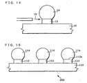
- FIG. 15 is a sectional view that schematically shows a micro lens substrate 200 of Example 1.
- FIG. 16 is a plan view that schematically shows the micro lens substrate 200 shown in FIG. 15. Moreover, FIG. 15 schematically shows a cross-section along line A - A in FIG. 16.
- the micro lens substrate 200 has a plurality of optical members 114 disposed thereupon.
- the optical members 114 are disposed on a top surface 112a of a base member 112.
- the base members 112 are formed upon a substrate 110.
- the substrate 110 is a glass substrate
- the base members 112 are a polyimide resin
- the optical members 114 consist of an ultraviolet cured resin.
- the perimeter of the optical members 114 is embedded using a sealing material 160 (FIG. 26).
- the perimeter of the optical members 114 in Examples 2 and 3 below may also, where necessary, be embedded using a sealing material 160.
- the sealing material 160 preferably consists of a material having a smaller refractive index than the material that comprises the optical members 114.
- the material of the sealing material 160 is not specifically prescribed, but a resin, for example, may be used.
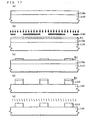
- FIG. 17(a) to- FIG. 17(e), as well as FIG. 18(a) and FIG. 18(b), are sectional views that schematically show the process for manufacturing the micro lens substrate 200 shown in FIG. 15 and FIG. 16, respectively.
- the substrate 110 which consists of a glass substrate
- the substrate 110 is heat treated at approximately 150 °C [FIG. 17(a)].
- a resin layer 112x is thereby formed. Although it can maintain its shape at this point in time, the resin layer 112x is not completely cured.
- a photolithography step is performed using a mask 130 having a prescribed pattern [FIG. 17(b)].
- a resist layer R1 of the prescribed pattern is thereby formed [FIG. 17(c)].
- the resin layer 112x is patterned by, for example, wet etching using an alkaline solution.
- the base members 112 are thereby formed [FIG. 17(d)].
- the resist layer R1 is stripped, after which heat treatment at approximately 350 °C is performed, thereby completely curing the base members 112 [FIG. 17(e)].
- a droplet 114b of a liquid material for forming the optical member 114 is ejected onto the top surface 112a of each base member 112 so as to form the optical member precursor (lens precursor) 114a.
- This optical member precursor 114a is converted to an optical member 114 (FIG. 15 and FIG. 16) by a subsequent curing process.
- a precursor of an ultraviolet cured resin is used as the liquid material, and an inkjet method is used as the method for ejecting the droplets 114b.
- the optical member precursor 114a of the desired shape and size is formed on the top surface 112a of the base member 112 by ejecting a plurality of droplets 114b.
- the droplets 114b are ejected until a cross section of the optical member 114 becomes greater than a cross section of the top surface 112a.
- the optical member 114 is formed by irradiating the optical member precursor 114a with ultraviolet rays 115 [FIG. 18(b)].
- the amount of ultraviolet irradiation is suitably adjusted according to the shape, size, and material of the optical member precursor 114a.
- the optical members (lenses) 114 are formed by the aforesaid process.
- the micro lens substrate 200 that includes the optical member 114 is thus obtained (FIG. 15 and FIG. 16).
- micro lens substrate 200 of the present example and its method of manufacture achieve the same effect as that achieved by the optical component and its method for manufacture.
- FIG. 19 is a sectional view that schematically shows a micro lens substrate 300 of Example 2.
- FIG. 20 is a plan view that schematically shows the micro lens substrate 300 shown in FIG. 19.
- FIG. 19 schematically shows a cross-section along line A - A in FIG. 20.
- the micro lens substrate 300 of the present example is structurally different from that of the micro lens substrate 200 of Example 1 in that base members 132 have an awning-type shape.
- the base members 132 consist of a polyimide resin. As shown in FIG. 19 and FIG. 20, the base members 132 have an awning-type shape. In other words, an upper part 132c of the base members 132 is formed in an inverse tapered shape. In this case, an acute angle ⁇ is formed between each base member's top surface 132a and its side surface 132b (the surface within the side member of the base member 132 that is adjacent to the top surface 132a). According to this configuration, the angle ⁇ formed between a base member's top surface 132a and side surface 132 can by made smaller. This can reliably prevent the side surface 132b of the base members 132 from being wetted by droplets and, thus, optical members 114 having the desired shape and size can be reliably formed.
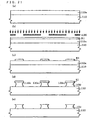
- FIG. 21(a) -to FIG. 21(e) are sectional views that schematically show the process for manufacturing the micro lens substrate 300 shown in FIG. 19 and FIG. 20, respectively.
- the method for manufacturing the micro lens substrate 300 of the present example is the same as the method for manufacturing the micro lens substrate 200 of Example 1, except for a step for patterning the base members 132. For this reason, the following description primarily concerns the step for patterning the base members 132.
- the resist layer R1 of a prescribed pattern is formed [FIG. 21(a) -to FIG. 21(c)]. The steps up to this point are the same as those in the manufacturing method described in Example 1.
- the substrate 110 is then heat treated at a temperature (130 °C, for example) that is just low enough not to change the properties of the resist.
- a temperature 130 °C, for example
- the resin layer 112x is wet-etched, using the resist layer R1 as a mask.
- the region directly beneath the resist layer that is, the top part of the resin layer 112x, is more resistant to etching, because the etchant penetrates more slowly here than in other regions.
- the top side portion of the resin layer 112x is cured to a greater degree by the heat treatment than is the substrate 110 side portion. Therefore, the wet-etch rate of the top side portion of the resin layer 112x is slower than that of the substrate 110 side portion.
- the subsequent steps are the same as those in the manufacturing method described in Example 1.
- the micro lens substrate 300 is thereby obtained (FIG. 19 and FIG. 20).
- micro lens substrate 300 of the present example and its method of manufacture achieve the same effect as that of the optical component and its method for manufacture.
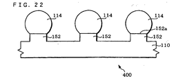
- FIG. 22 is a sectional view that schematically shows a micro lens substrate 400 of Example 3.
- FIG. 23 is a plan view that schematically shows the micro lens substrate 400 shown in FIG. 22.
- FIG. 22 schematically shows a cross-section along line A - A in FIG. 23.
- the micro lens substrate 400 of the present example has a configuration that differs from that in Example 1 in that base members 152 are formed so that they are integral with the substrate 110 and are made from the same material (a glass substrate) as the substrate 110.
- the other constituent elements are structurally the same as those in the micro lens substrate 200 of Example 1, so their description is omitted here.
- FIG. 24(a) -to FIG. 24(e) are sectional views that schematically show the process for manufacturing the micro lens substrate 400 shown in FIG. 22 and FIG. 23, respectively.
- a dry film resist (DFR) is laminated on the substrate 110, which consists of a glass substrate [FIG. 24(a)].
- the substrate 110 which consists of a glass substrate, is patterned, using the resist layer R2 as a mask [FIG. 24(d)].
- This patterning thus forms the base members 152 so that they are integrated with the substrate 110. In other words, adjacent base members 152 are separated by a channel.
- Examples of possible patterning methods include wet etching with hydrofluoric acid, ion beam etching, micro fabrication with a laser, sandblasting, and so forth.
- sandblasting is among the more effective techniques.
- Sandblasting a technique wherein etching is performed by blasting the work piece with particles whose diameter ranges from 1 micron to several tens of microns, can obtain resolutions of about 20 microns. Examples of materials that can be used as particles in sandblasting are SiC and AlO 2 and so forth.
- the resist layer R2 is stripped [FIG. 24(e)].
- the subsequent steps are the same as those in the manufacturing method described in Example 1.
- the micro lens substrate 400 is thereby obtained (FIG. 22 and FIG. 23).
- micro lens substrate 400 of the present example and its method of manufacture achieves the same effect as that of the optical component and its method for manufacture.
- Example 4 describes a method for removing the optical members 14 from the micro lens substrate 200 obtained in Example 1.
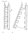
- FIG. 25(a) and FIG. 25(b) are sectional views that respectively schematically show a method for removing the optical members 114 of the present example.
- the removed optical members 114 can be used independently as a part of another device.
- the optical member 114 can be used as a ball lens, as a part of another device.
- an adhesive sheet 150 is placed on the optical members 114 of the micro lens substrate 200 of Example 1 [FIG. 25(a)]. Then, the optical members 114 are removed from the base member 112 by pulling off the adhesive sheet 150 [FIG. 25(b)]. The optical members 114 can be removed by the aforesaid process. If the top surface 112a of the base members 112 was pre-treated with a repellant liquid, removal is facilitated.
- the present example describes a method for removing the optical members 114 from the micro lens substrate 200 of Example 1.
- the method of the present example may also be used to remove the optical members 114 from the micro lens substrates 300, 400 of Examples 2 and 3.
- the present example describes a method for removing optical members that function as lenses from the micro lens substrate.
- a method similar to that in the present example may also be used for instances where optical members having functions other than those of lenses are to be removed from the optical component.
Landscapes
- Physics & Mathematics (AREA)
- Engineering & Computer Science (AREA)
- General Physics & Mathematics (AREA)
- Optics & Photonics (AREA)
- Manufacturing & Machinery (AREA)
- Ophthalmology & Optometry (AREA)
- Health & Medical Sciences (AREA)
- Mechanical Engineering (AREA)
- Condensed Matter Physics & Semiconductors (AREA)
- Computer Hardware Design (AREA)
- Microelectronics & Electronic Packaging (AREA)
- Power Engineering (AREA)
- Optical Elements Other Than Lenses (AREA)
- Casting Or Compression Moulding Of Plastics Or The Like (AREA)
Applications Claiming Priority (3)
| Application Number | Priority Date | Filing Date | Title |
|---|---|---|---|
| JP2002279064A JP3719431B2 (ja) | 2002-09-25 | 2002-09-25 | 光学部品およびその製造方法、表示装置および撮像素子 |
| JP2002279064 | 2002-09-25 | ||
| EP03019615A EP1411376B1 (en) | 2002-09-25 | 2003-09-04 | Method of manufacturing an optical component |
Related Parent Applications (2)
| Application Number | Title | Priority Date | Filing Date |
|---|---|---|---|
| EP03019615.8 Division | 2003-09-04 | ||
| EP03019615A Division EP1411376B1 (en) | 2002-09-25 | 2003-09-04 | Method of manufacturing an optical component |
Publications (2)
| Publication Number | Publication Date |
|---|---|
| EP1582892A1 EP1582892A1 (en) | 2005-10-05 |
| EP1582892B1 true EP1582892B1 (en) | 2008-01-23 |
Family
ID=32040444
Family Applications (2)
| Application Number | Title | Priority Date | Filing Date |
|---|---|---|---|
| EP05011306A Expired - Lifetime EP1582892B1 (en) | 2002-09-25 | 2003-09-04 | Optical component |
| EP03019615A Expired - Lifetime EP1411376B1 (en) | 2002-09-25 | 2003-09-04 | Method of manufacturing an optical component |
Family Applications After (1)
| Application Number | Title | Priority Date | Filing Date |
|---|---|---|---|
| EP03019615A Expired - Lifetime EP1411376B1 (en) | 2002-09-25 | 2003-09-04 | Method of manufacturing an optical component |
Country Status (6)
| Country | Link |
|---|---|
| US (1) | US7179728B2 (enExample) |
| EP (2) | EP1582892B1 (enExample) |
| JP (1) | JP3719431B2 (enExample) |
| KR (1) | KR100739085B1 (enExample) |
| CN (1) | CN1490635A (enExample) |
| DE (2) | DE60302526T2 (enExample) |
Families Citing this family (31)
| Publication number | Priority date | Publication date | Assignee | Title |
|---|---|---|---|---|
| JP4088779B2 (ja) | 2003-04-25 | 2008-05-21 | セイコーエプソン株式会社 | 光ファイバ間の結合構造および結合方法 |
| JP4155099B2 (ja) * | 2003-05-16 | 2008-09-24 | セイコーエプソン株式会社 | マイクロレンズの製造方法 |
| JP3800199B2 (ja) * | 2003-05-16 | 2006-07-26 | セイコーエプソン株式会社 | マイクロレンズの製造方法 |
| JP4120813B2 (ja) | 2003-06-12 | 2008-07-16 | セイコーエプソン株式会社 | 光学部品およびその製造方法 |
| JP3719441B2 (ja) | 2003-08-01 | 2005-11-24 | セイコーエプソン株式会社 | 光素子およびその製造方法、光モジュール、光伝達装置 |
| JP4241259B2 (ja) * | 2003-08-06 | 2009-03-18 | セイコーエプソン株式会社 | マイクロレンズの製造方法 |
| KR100589225B1 (ko) * | 2004-05-31 | 2006-06-19 | 엘지전자 주식회사 | 향상된 시야각을 갖는 마이크로렌즈 배열 시트 |
| DE102004030418A1 (de) * | 2004-06-24 | 2006-01-19 | Robert Bosch Gmbh | Mikrostrukturierter Infrarot-Sensor und ein Verfahren zu seiner Herstellung |
| JP2006030634A (ja) * | 2004-07-16 | 2006-02-02 | Seiko Epson Corp | マイクロレンズの製造方法 |
| KR100636349B1 (ko) | 2004-09-24 | 2006-10-19 | 엘지전자 주식회사 | 마이크로렌즈 배열 시트 및 그 제작방법 |
| JP2006323147A (ja) * | 2005-05-19 | 2006-11-30 | Seiko Epson Corp | マイクロレンズの製造方法、マイクロレンズ、及び光学膜、プロジェクション用スクリーン、プロジェクターシステム、電気光学装置、電子機器 |
| JP2006350177A (ja) * | 2005-06-20 | 2006-12-28 | Seiko Epson Corp | 光学シートの製造方法、光学シート、面状照明装置、電気光学装置 |
| JP2007010707A (ja) * | 2005-06-28 | 2007-01-18 | Seiko Epson Corp | 光学シートの製造方法、光学シート、バックライトユニット、表示装置、電子機器 |
| JP2007036140A (ja) * | 2005-07-29 | 2007-02-08 | Seiko Epson Corp | 光素子およびその製造方法 |
| JP2007080884A (ja) * | 2005-09-09 | 2007-03-29 | Asahi Glass Co Ltd | 発光装置の製造方法、発光装置および発光装置の中間部品 |
| KR100774218B1 (ko) * | 2006-09-28 | 2007-11-08 | 엘지전자 주식회사 | 렌즈, 그 제조방법 및 발광 소자 패키지 |
| US8115920B2 (en) * | 2007-11-14 | 2012-02-14 | 3M Innovative Properties Company | Method of making microarrays |
| CN100583477C (zh) * | 2008-07-10 | 2010-01-20 | 盛扬光电股份有限公司 | 可置换透镜的发光二极管透镜模块结构 |
| JP2010223975A (ja) * | 2009-03-19 | 2010-10-07 | Dhs:Kk | レンズアレイの製造方法及びレンズアレイ |
| JP2011076800A (ja) * | 2009-09-29 | 2011-04-14 | Fujifilm Corp | 有機el素子及びその製造方法 |
| MX2013011770A (es) * | 2011-04-12 | 2014-08-01 | Pixeloptics Inc | Mejora de perfil de suministro de adhesivo. |
| JP2013037164A (ja) * | 2011-08-08 | 2013-02-21 | Sony Corp | 拡散シート、バックライト、液晶表示装置および拡散シートの製造方法 |
| TW201316383A (zh) * | 2011-10-12 | 2013-04-16 | Univ Nat Taiwan | 於非soi基板上製作矽波導之方法 |
| US8828484B2 (en) * | 2013-01-28 | 2014-09-09 | Taiwan Semiconductor Manufacturing Co., Ltd. | Self-alignment due to wettability difference of an interface |
| WO2015069283A1 (en) * | 2013-11-08 | 2015-05-14 | Empire Technology Development Llc | Printed ball lens and methods for their fabrication |
| CN105116612B (zh) * | 2015-09-22 | 2018-05-18 | 京东方科技集团股份有限公司 | 光学膜片、背光模组及显示装置 |
| US9804367B2 (en) | 2015-11-04 | 2017-10-31 | Omnivision Technologies, Inc. | Wafer-level hybrid compound lens and method for fabricating same |
| CN106526722B (zh) * | 2016-11-09 | 2018-04-24 | 中南大学 | 一种控制微型液滴形状的方法 |
| KR102095003B1 (ko) | 2017-01-03 | 2020-03-30 | 주식회사 엘지화학 | 수지 입자의 제조 방법 |
| DE102017003721A1 (de) * | 2017-03-01 | 2018-09-06 | Docter Optics Se | Verfahren zum Herstellen eines Mikroprojektors für ein Projektionsdisplay |
| KR102167540B1 (ko) * | 2018-05-21 | 2020-10-20 | (주)유니젯 | 다층기판의 제조방법 |
Family Cites Families (34)
| Publication number | Priority date | Publication date | Assignee | Title |
|---|---|---|---|---|
| US4689291A (en) * | 1985-08-30 | 1987-08-25 | Xerox Corporation | Pedestal-type microlens fabrication process |
| JPS6283337A (ja) | 1985-10-04 | 1987-04-16 | Hoya Corp | マイクロレンズアレ−の製造方法 |
| JPH02165932A (ja) | 1988-12-20 | 1990-06-26 | Seiko Epson Corp | マイクロレンズアレイの製造方法 |
| US5229016A (en) * | 1991-08-08 | 1993-07-20 | Microfab Technologies, Inc. | Method and apparatus for dispensing spherical-shaped quantities of liquid solder |
| JP3198003B2 (ja) | 1993-12-24 | 2001-08-13 | 学校法人桐蔭学園 | 耐光性フィブロイン−天然色素複合体 |
| US5498444A (en) * | 1994-02-28 | 1996-03-12 | Microfab Technologies, Inc. | Method for producing micro-optical components |
| JPH0882759A (ja) | 1994-09-09 | 1996-03-26 | Canon Inc | 走査光学装置 |
| JP3241251B2 (ja) * | 1994-12-16 | 2001-12-25 | キヤノン株式会社 | 電子放出素子の製造方法及び電子源基板の製造方法 |
| US5846694A (en) * | 1996-02-13 | 1998-12-08 | The Regents Of The University Of California | Microminiature optical waveguide structure and method for fabrication |
| JP3764199B2 (ja) | 1996-03-05 | 2006-04-05 | 株式会社リコー | 光源装置 |
| GB9611582D0 (en) * | 1996-06-04 | 1996-08-07 | Thin Film Technology Consultan | 3D printing and forming of structures |
| JP3786427B2 (ja) | 1996-09-19 | 2006-06-14 | セイコーエプソン株式会社 | 発光装置の製造方法 |
| DE19712297A1 (de) | 1997-03-24 | 1998-10-01 | Bosch Gmbh Robert | Verfahren zur Herstellung von lichtführenden Strukturen |
| JP3920461B2 (ja) | 1998-06-15 | 2007-05-30 | 大日本印刷株式会社 | レンズおよびその製造方法 |
| EP1376225B1 (en) | 1997-08-08 | 2010-10-13 | Dai Nippon Printing Co., Ltd. | Structure for pattern formation, method for pattern formation, and application thereof |
| DE69840914D1 (de) * | 1997-10-14 | 2009-07-30 | Patterning Technologies Ltd | Methode zur Herstellung eines elektrischen Kondensators |
| JP4217294B2 (ja) | 1998-04-28 | 2009-01-28 | Hoya株式会社 | 光学素子の接着装置 |
| US6074888A (en) | 1998-08-18 | 2000-06-13 | Trw Inc. | Method for fabricating semiconductor micro epi-optical components |
| JP2000108216A (ja) | 1998-10-02 | 2000-04-18 | Canon Inc | マイクロレンズアレイの製造方法 |
| JP4275233B2 (ja) | 1999-01-06 | 2009-06-10 | 大日本印刷株式会社 | 光学素子およびその製造方法 |
| JP2000280367A (ja) | 1999-03-30 | 2000-10-10 | Seiko Epson Corp | マイクロレンズの製造装置及び製造方法 |
| JP2001208958A (ja) | 2000-01-26 | 2001-08-03 | Fuji Photo Film Co Ltd | 光学装置 |
| US20010048968A1 (en) | 2000-02-16 | 2001-12-06 | Cox W. Royall | Ink-jet printing of gradient-index microlenses |
| US6625351B2 (en) | 2000-02-17 | 2003-09-23 | Microfab Technologies, Inc. | Ink-jet printing of collimating microlenses onto optical fibers |
| TW463058B (en) * | 2000-10-20 | 2001-11-11 | Ind Tech Res Inst | Method for fabricating microlens in batch and product manufactured the same |
| JP3899879B2 (ja) | 2000-11-21 | 2007-03-28 | セイコーエプソン株式会社 | カラーフィルタの製造方法及び製造装置、液晶装置の製造方法及び製造装置、el装置の製造方法及び製造装置、インクジェットヘッドの制御装置、材料の吐出方法及び材料の吐出装置、並びに電子機器 |
| JP3491155B2 (ja) | 2000-11-21 | 2004-01-26 | セイコーエプソン株式会社 | 材料の吐出方法、及び吐出装置、カラーフィルタの製造方法及び製造装置、液晶装置の製造方法及び製造装置、el装置の製造方法及び製造装置 |
| JP2002169004A (ja) | 2000-11-29 | 2002-06-14 | Ind Technol Res Inst | バッチ生産マイクロレンズアレイ及びその製造方法 |
| JP2002202426A (ja) | 2000-12-28 | 2002-07-19 | Matsushita Electric Ind Co Ltd | 光導波路の製造方法 |
| CN1193249C (zh) | 2001-02-12 | 2005-03-16 | 财团法人工业技术研究院 | 整体化微球透镜的光纤对准元件 |
| GB2373095A (en) * | 2001-03-09 | 2002-09-11 | Seiko Epson Corp | Patterning substrates with evaporation residues |
| JP3998921B2 (ja) | 2001-05-11 | 2007-10-31 | 日本電信電話株式会社 | マイクロレンズ形成方法 |
| JP4141674B2 (ja) | 2001-10-22 | 2008-08-27 | セイコーエプソン株式会社 | 液滴吐出ヘッド、その拭取り方法およびこれを備えた電子機器 |
| JP4161590B2 (ja) | 2002-02-22 | 2008-10-08 | セイコーエプソン株式会社 | マイクロレンズの製造方法、マイクロレンズ、光学膜、プロジェクション用スクリーン、及びプロジェクターシステム |
-
2002
- 2002-09-25 JP JP2002279064A patent/JP3719431B2/ja not_active Expired - Fee Related
-
2003
- 2003-08-28 US US10/649,891 patent/US7179728B2/en not_active Expired - Fee Related
- 2003-09-04 DE DE60302526T patent/DE60302526T2/de not_active Expired - Lifetime
- 2003-09-04 EP EP05011306A patent/EP1582892B1/en not_active Expired - Lifetime
- 2003-09-04 DE DE60318905T patent/DE60318905T2/de not_active Expired - Lifetime
- 2003-09-04 EP EP03019615A patent/EP1411376B1/en not_active Expired - Lifetime
- 2003-09-16 CN CNA031569722A patent/CN1490635A/zh active Pending
- 2003-09-24 KR KR1020030066127A patent/KR100739085B1/ko not_active Expired - Fee Related
Also Published As
| Publication number | Publication date |
|---|---|
| DE60302526T2 (de) | 2006-08-10 |
| EP1411376B1 (en) | 2005-11-30 |
| DE60302526D1 (de) | 2006-01-05 |
| KR100739085B1 (ko) | 2007-07-13 |
| DE60318905T2 (de) | 2009-01-29 |
| EP1411376A1 (en) | 2004-04-21 |
| US7179728B2 (en) | 2007-02-20 |
| JP2004117660A (ja) | 2004-04-15 |
| US20040106223A1 (en) | 2004-06-03 |
| JP3719431B2 (ja) | 2005-11-24 |
| CN1490635A (zh) | 2004-04-21 |
| KR20040027369A (ko) | 2004-04-01 |
| EP1582892A1 (en) | 2005-10-05 |
| DE60318905D1 (de) | 2008-03-13 |
Similar Documents
| Publication | Publication Date | Title |
|---|---|---|
| EP1582892B1 (en) | Optical component | |
| US7145725B2 (en) | Micro lens and fabrication method of micro lens, optical device, optical transmitter, laser printer head, and laser printer | |
| CN100403064C (zh) | 光学部件及其制造方法 | |
| CN100541947C (zh) | 具有集成透镜的垂直腔表面发射激光器 | |
| KR100615934B1 (ko) | 마이크로 렌즈의 제조 방법 및 마이크로 렌즈, 광학 장치,광전송 장치, 레이저 프린터용 헤드, 레이저 프린터 | |
| WO2002027363A2 (en) | Method of bonding wafers with controlled height and associated structures | |
| US20040257660A1 (en) | Method of manufacturing micro lens, micro lens, optical device, optical transmission device, head for laser printer, and laser printer | |
| KR100648052B1 (ko) | 마이크로 렌즈의 제조 방법 및 마이크로 렌즈, 광학 장치,광전송 장치, 레이저 프린터용 헤드, 및 레이저 프린터 | |
| JP4114060B2 (ja) | 受光素子の製造方法 | |
| JP2009265275A (ja) | 光路変換ミラー及びその作製方法 | |
| US7197212B2 (en) | Optical waveguide and method of manufacturing the same, circuit board, optical module, and optical transfer apparatus | |
| JP4088779B2 (ja) | 光ファイバ間の結合構造および結合方法 | |
| JP2004271702A (ja) | 光学部品およびその製造方法、マイクロレンズ基板、表示装置、撮像素子、光素子、光モジュール | |
| JP2006011465A (ja) | 光学部品およびその製造方法、マイクロレンズ基板およびその製造方法、表示装置、撮像素子 | |
| JP4381125B2 (ja) | 光学部品の製造方法 | |
| JP2004198514A (ja) | 光学部品およびその製造方法、マイクロレンズ基板、表示装置、撮像素子、光素子、光モジュール | |
| JP2005181417A (ja) | 光学部品およびその製造方法 | |
| JP2005277312A (ja) | Msm型受光素子およびその製造方法、光モジュール、並びに、光伝達装置 | |
| JP2007258730A (ja) | 受光素子、光モジュール、光伝達装置 |
Legal Events
| Date | Code | Title | Description |
|---|---|---|---|
| PUAI | Public reference made under article 153(3) epc to a published international application that has entered the european phase |
Free format text: ORIGINAL CODE: 0009012 |
|
| AC | Divisional application: reference to earlier application |
Ref document number: 1411376 Country of ref document: EP Kind code of ref document: P |
|
| AK | Designated contracting states |
Kind code of ref document: A1 Designated state(s): DE FR GB NL |
|
| 17P | Request for examination filed |
Effective date: 20050927 |
|
| AKX | Designation fees paid |
Designated state(s): DE FR GB NL |
|
| 17Q | First examination report despatched |
Effective date: 20051111 |
|
| GRAP | Despatch of communication of intention to grant a patent |
Free format text: ORIGINAL CODE: EPIDOSNIGR1 |
|
| GRAS | Grant fee paid |
Free format text: ORIGINAL CODE: EPIDOSNIGR3 |
|
| GRAA | (expected) grant |
Free format text: ORIGINAL CODE: 0009210 |
|
| AC | Divisional application: reference to earlier application |
Ref document number: 1411376 Country of ref document: EP Kind code of ref document: P |
|
| AK | Designated contracting states |
Kind code of ref document: B1 Designated state(s): DE FR GB NL |
|
| REG | Reference to a national code |
Ref country code: GB Ref legal event code: FG4D |
|
| REF | Corresponds to: |
Ref document number: 60318905 Country of ref document: DE Date of ref document: 20080313 Kind code of ref document: P |
|
| ET | Fr: translation filed | ||
| PLBE | No opposition filed within time limit |
Free format text: ORIGINAL CODE: 0009261 |
|
| STAA | Information on the status of an ep patent application or granted ep patent |
Free format text: STATUS: NO OPPOSITION FILED WITHIN TIME LIMIT |
|
| 26N | No opposition filed |
Effective date: 20081024 |
|
| REG | Reference to a national code |
Ref country code: FR Ref legal event code: PLFP Year of fee payment: 14 |
|
| REG | Reference to a national code |
Ref country code: FR Ref legal event code: PLFP Year of fee payment: 15 |
|
| PGFP | Annual fee paid to national office [announced via postgrant information from national office to epo] |
Ref country code: NL Payment date: 20170814 Year of fee payment: 15 |
|
| PGFP | Annual fee paid to national office [announced via postgrant information from national office to epo] |
Ref country code: DE Payment date: 20170830 Year of fee payment: 15 Ref country code: FR Payment date: 20170810 Year of fee payment: 15 Ref country code: GB Payment date: 20170830 Year of fee payment: 15 |
|
| REG | Reference to a national code |
Ref country code: DE Ref legal event code: R119 Ref document number: 60318905 Country of ref document: DE |
|
| REG | Reference to a national code |
Ref country code: NL Ref legal event code: MM Effective date: 20181001 |
|
| GBPC | Gb: european patent ceased through non-payment of renewal fee |
Effective date: 20180904 |
|
| PG25 | Lapsed in a contracting state [announced via postgrant information from national office to epo] |
Ref country code: NL Free format text: LAPSE BECAUSE OF NON-PAYMENT OF DUE FEES Effective date: 20181001 |
|
| PG25 | Lapsed in a contracting state [announced via postgrant information from national office to epo] |
Ref country code: DE Free format text: LAPSE BECAUSE OF NON-PAYMENT OF DUE FEES Effective date: 20190402 |
|
| PG25 | Lapsed in a contracting state [announced via postgrant information from national office to epo] |
Ref country code: FR Free format text: LAPSE BECAUSE OF NON-PAYMENT OF DUE FEES Effective date: 20180930 |
|
| PG25 | Lapsed in a contracting state [announced via postgrant information from national office to epo] |
Ref country code: GB Free format text: LAPSE BECAUSE OF NON-PAYMENT OF DUE FEES Effective date: 20180904 |