EP1580885B1 - Oberflächenwellenvorrichtung und Prozess zu ihrer Herstellung - Google Patents
Oberflächenwellenvorrichtung und Prozess zu ihrer Herstellung Download PDFInfo
- Publication number
- EP1580885B1 EP1580885B1 EP05005257A EP05005257A EP1580885B1 EP 1580885 B1 EP1580885 B1 EP 1580885B1 EP 05005257 A EP05005257 A EP 05005257A EP 05005257 A EP05005257 A EP 05005257A EP 1580885 B1 EP1580885 B1 EP 1580885B1
- Authority
- EP
- European Patent Office
- Prior art keywords
- acoustic wave
- grooves
- grinding
- surface acoustic
- piezoelectric substrate
- Prior art date
- Legal status (The legal status is an assumption and is not a legal conclusion. Google has not performed a legal analysis and makes no representation as to the accuracy of the status listed.)
- Expired - Lifetime
Links
- 238000010897 surface acoustic wave method Methods 0.000 title claims description 133
- 238000000034 method Methods 0.000 title claims description 37
- 239000000758 substrate Substances 0.000 claims description 88
- 230000003746 surface roughness Effects 0.000 claims description 48
- 230000001902 propagating effect Effects 0.000 claims description 42
- 230000003247 decreasing effect Effects 0.000 claims description 11
- 235000012431 wafers Nutrition 0.000 description 67
- 230000000694 effects Effects 0.000 description 24
- 230000002411 adverse Effects 0.000 description 23
- 239000011295 pitch Substances 0.000 description 13
- 230000000644 propagated effect Effects 0.000 description 8
- 238000004519 manufacturing process Methods 0.000 description 3
- 238000005452 bending Methods 0.000 description 2
- 238000004140 cleaning Methods 0.000 description 2
- 238000012986 modification Methods 0.000 description 2
- 230000004048 modification Effects 0.000 description 2
- 238000005498 polishing Methods 0.000 description 2
- XLYOFNOQVPJJNP-UHFFFAOYSA-N water Substances O XLYOFNOQVPJJNP-UHFFFAOYSA-N 0.000 description 2
- 229910003327 LiNbO3 Inorganic materials 0.000 description 1
- 229910012463 LiTaO3 Inorganic materials 0.000 description 1
- 230000015556 catabolic process Effects 0.000 description 1
- 238000004891 communication Methods 0.000 description 1
- 238000006731 degradation reaction Methods 0.000 description 1
- 229910003460 diamond Inorganic materials 0.000 description 1
- 239000010432 diamond Substances 0.000 description 1
- 239000000463 material Substances 0.000 description 1
- 230000001681 protective effect Effects 0.000 description 1
Images


Classifications
-
- H—ELECTRICITY
- H03—ELECTRONIC CIRCUITRY
- H03H—IMPEDANCE NETWORKS, e.g. RESONANT CIRCUITS; RESONATORS
- H03H9/00—Networks comprising electromechanical or electro-acoustic elements; Electromechanical resonators
- H03H9/46—Filters
- H03H9/64—Filters using surface acoustic waves
-
- H—ELECTRICITY
- H03—ELECTRONIC CIRCUITRY
- H03H—IMPEDANCE NETWORKS, e.g. RESONANT CIRCUITS; RESONATORS
- H03H9/00—Networks comprising electromechanical or electro-acoustic elements; Electromechanical resonators
- H03H9/02—Details
- H03H9/02535—Details of surface acoustic wave devices
- H03H9/02614—Treatment of substrates, e.g. curved, spherical, cylindrical substrates ensuring closed round-about circuits for the acoustical waves
- H03H9/02622—Treatment of substrates, e.g. curved, spherical, cylindrical substrates ensuring closed round-about circuits for the acoustical waves of the surface, including back surface
-
- H—ELECTRICITY
- H03—ELECTRONIC CIRCUITRY
- H03H—IMPEDANCE NETWORKS, e.g. RESONANT CIRCUITS; RESONATORS
- H03H3/00—Apparatus or processes specially adapted for the manufacture of impedance networks, resonating circuits, resonators
- H03H3/007—Apparatus or processes specially adapted for the manufacture of impedance networks, resonating circuits, resonators for the manufacture of electromechanical resonators or networks
- H03H3/08—Apparatus or processes specially adapted for the manufacture of impedance networks, resonating circuits, resonators for the manufacture of electromechanical resonators or networks for the manufacture of resonators or networks using surface acoustic waves
-
- H—ELECTRICITY
- H03—ELECTRONIC CIRCUITRY
- H03H—IMPEDANCE NETWORKS, e.g. RESONANT CIRCUITS; RESONATORS
- H03H9/00—Networks comprising electromechanical or electro-acoustic elements; Electromechanical resonators
- H03H9/25—Constructional features of resonators using surface acoustic waves
-
- Y—GENERAL TAGGING OF NEW TECHNOLOGICAL DEVELOPMENTS; GENERAL TAGGING OF CROSS-SECTIONAL TECHNOLOGIES SPANNING OVER SEVERAL SECTIONS OF THE IPC; TECHNICAL SUBJECTS COVERED BY FORMER USPC CROSS-REFERENCE ART COLLECTIONS [XRACs] AND DIGESTS
- Y10—TECHNICAL SUBJECTS COVERED BY FORMER USPC
- Y10T—TECHNICAL SUBJECTS COVERED BY FORMER US CLASSIFICATION
- Y10T29/00—Metal working
- Y10T29/42—Piezoelectric device making
Definitions
- the present invention relates to a surface acoustic wave device, and a process for fabricating the same.
- a surface acoustic wave device such as a surface acoustic wave (SAW) filter has a comb transducer comprised of an electrode pair on a transmitting side (simply called as “transmitting electrode”) and an electrode pair on a receiving side (simply called as “receiving electrode”) on a surface of a piezoelectric substrate.
- the transmitting electrode and the receiving electrode each has a pair of electrodes constructed such that an anode and a cathode intersect with each other.
- a surface acoustic wave excited by the transmitting electrode is propagated over the surface of the piezoelectric substrate, and is received by the receiving electrode for output.
- 56-132806 discloses a technique in which plural grooves extending in a direction intersecting with the propagating direction of a surface acoustic wave are formed in a back surface of a piezoelectric substrate to vary the reflecting directions of the unnecessary wave on the back surface of the substrate for the purpose of reducing the unnecessary wave signal and suppressing adverse effects of the unnecessary wave signal.
- the grooves for reducing the unnecessary wave signal are generally formed by a diamond cutter or a router, the grooves have a linear configuration and are formed equidistantly spaced apart from each other. Therefore, the reflecting conditions of the unnecessary wave to the respective grooves are identical to each other, which makes it difficult to provide advanced measures for reducing the unnecessary wave signal.
- Document DE 196 26 410 A1 discloses a substrate for an SAW device with slit-like depressions deviating from a straight-line run on the surface side opposite to the surface side guiding a surface acoustic wave.
- Document EP 0704812 A2 discloses a SAW device with a substrate having a roughness configuration on a back face thereof and a maximum depth of the roughness configuration is not less than a wavelength of bulk waves of convolution output taken out of the output electrode.
- US patent 3,283,264 discloses a frequency selective system for ultrasonic wave energy and more particularly to simple ultrasonic delay line structures employing the principles of diffraction gratings.
- An aspect of the invention is directed to a surface acoustic wave device oomprising: a piezoelectric substrate; a comb transducer which is formed on a surface of the piezoelectric substrate; and a plurality of grooves which are formed in a back surface of the piezoelectric substrate in a direction intersecting with a propagating direction of a surface acoustic wave, wherein, for each groove an interval of the adjoining grooves being decreased as the groove extends from one end of the piezoelectric substrate to the other end thereof, wherein the one end and the other end are each located on a side substantially perpendicular to the propagating direction of the surface acoustic wave.
- the plurality of grooves are formed in the back surface of the piezoelectric substrate. Since the grooves extend in the direction intersecting with the propagating direction of the surface acoustic wave, unlike an arrangement that grooves extend substantially parallel to the propagating direction of the surface acoustic wave, this arrangement enables to increase the degree of variance of reflection of the surface acoustic wave (unnecessary wave) that has been sent from the transmitting electrode of the comb transducer and reached the back surface of the substrate. Thus, there is no or less likelihood that the unnecessary wave reflected on the grooves may be received by the receiving electrode of the comb transducer, and the surface acoustic wave device exhibits good device characteristics with less or no noise.
- the grooves are formed in such a manner that the interval of the adjoining grooves is decreased as the groove extends from one end of the surface acoustic wave device toward the other end thereof, wherein the one end and the other end are each located on a side substantially perpendicular to the propagating direction of the surface acoustic wave.
- Another aspect of the invention is directed to a process for fabricating a surface acoustic wave device provided with a piezoelectric substrate, a comb transducer formed on a surface of the piezoelectric substrate, and a plurality of grooves formed in a back surface of the piezoelectric substrate in a direction intersecting with a propagating direction of a surface acoustic wave, the grooves being formed in such a manner that for each groove an interval of the adjoining grooves is decreased as the groove extends from one end of the piezoelectric substrate to the other end thereof, wherein the one end and the other end are each located on a side substantially perpendicular to the propagating direction of the surface acoustic wave, wherein the plurality of grooves are formed by grinding.
- the above arrangement enables to maximize the degree of variance of reflection of the unnecessary wave on the back surface of the piezoelectric substrate, and realize a surface acoustic wave device capable of effectively suppressing adverse effects of the unnecessary wave. Further, since the grinding technique is employed, a thick affected layer in which crystalline structure of the substrate is modified by a stress applied to the substrate in forming the plurality of grooves is formed in a region on the back side of the piezoelectric substrate. Since the unnecessary wave is reflected at random in the affected layer, adverse effects of the unnecessary wave can be effectively suppressed.
- a surface of a piezoelectric substrate which is opposite to a surface where electrodes are formed, and in which grooves are formed is referred to as "a back surface of the substrate”.
- FIG. 1 is a perspective view of a surface acoustic wave filter as an example of a surface acoustic wave device embodying the invention.
- the acoustic surface wave filter is constructed such that electrode pairs 2a and 2b constituting a comb transducer 2 are arranged opposing to each other on a piezoelectric substrate 1 made of LiTaO 3 or LiNbO 3 in a propagating direction of a surface acoustic wave 3.
- the surface of the piezoelectric substrate 1 is distorted by an electrical signal inputted to the electrode pair 2a on a transmitting side (hereinafter, called as “transmitting electrode 2a"), and the distortion is propagated as the surface acoustic wave 3 to the electrode pair 2b on a receiving side (hereinafter, called as “receiving electrode 2b").
- the surface acoustic wave 3 is converted into an electric signal by the receiving electrode 2b, whereby the surface acoustic wave filter exhibits filter characteristics.
- the thickness c of the piezoelectric substrate 1 is 0.15 mm, the shorter side a thereof is 0.7 mm, and the longer side b thereof is 1.3 mm.
- the wavelength of the surface acoustic wave to be propagated is equal to the pitch (shown by ⁇ in FIG. 1 ) between an anode and a cathode of the transmitting electrode 2a.
- V 0 f C ⁇
- ⁇ represents a wavelength of the surface acoustic wave 3
- f C represents a center frequency of the surface acoustic wave filter
- V 0 represents a velocity of a sound propagating through the piezoelectric substrate 1.
- the wavelength ⁇ is 2.1 ⁇ m
- the center frequency f C is 1842.5 MHz.
- FIG. 2 is a cross-sectional side view of the surface acoustic wave filter shown in FIG. 1 .
- the surface acoustic wave filter there is a wave 4 (called as "unnecessary wave 4") other than the surface acoustic wave 3 which is propagated over the surface of the piezoelectric substrate 1.
- the unnecessary wave 4 from the transmitting electrode 2a constituting the comb transducer 2 is propagated through the interior of the piezoelectric substrate 1, reflected on the back surface of the substrate 1, and is received by the receiving electrode 2b.
- plural linear grooves extending in a direction orthogonal to the propagating direction of a surface acoustic wave are formed in a back surface of a piezoelectric substrate to suppress such an unnecessary wave.
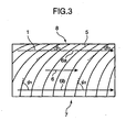
- FIG. 3 is a bottom view of the surface acoustic wave filter shown in FIGS. 1 and 2 .
- the extending direction of each groove 5 formed in the back surface of the piezoelectric substrate 1 substantially intersects with the propagating direction of the surface acoustic wave 3 shown by the arrow 6.
- the interval of the adjoining grooves 5 is reduced as the groove 5 extends from one end 7 of the substrate 1 toward the other end 8 of the substrate 1.
- the configuration of the curved grooves 5 is such that, as shown in FIG. 3 , when angles defined by tangential lines of arbitrary two grooves 5 at intersecting points at which the two grooves 5 intersect with a line segment 6a parallel to the propagating direction 6 of the surface acoustic wave 3, and the line segment 6a are ⁇ 1 and ⁇ 2 , respectively, these angles ⁇ 1 and ⁇ 2 are different from each other.
- the grooves 5 have curvatures with the same sign (+ or -), and that the curvature is increased as each groove 5 extends from the one end 7 of the substrate 1 toward the other end 8 thereof.
- This arrangement enables to increase the degree of variance of the unnecessary wave 4 that is reflected on the back surface of the piezoelectric substrate 1, as compared with the conventional arrangement having the linear grooves, thereby suppressing adverse effects of the unnecessary wave 4 to filter characteristics.
- the depth dof the groove 5 which is a value measured from the back surface of the piezoelectric substrate 1 shown in FIG. 2 , has a lower limit in accordance with the wavelength ⁇ of the surface acoustic wave 3, so that adverse effects of the unnecessary wave 4 can be effectively suppressed as far as the depth d lies in a certain range including the lower limit.
- the depth d of the groove 5 is not smaller than 0.5%, more preferably not smaller than 1.0%, and furthermore preferably, about 5.0% relative to the wavelength ⁇ of the surface acoustic wave 3.
- the unnecessary wave 4 is effectively scattered as far as the depth d of the groove 5 is not smaller than the aforementioned lower limit. Accordingly, there is no constraint regarding a relation to the wavelength ⁇ of the surface acoustic wave 3, as far as the depth d of the groove 5 satisfies the above requirement. However, if the depth d of the groove 5 transgresses an upper limit, it is likely that crack may be generated in the piezoelectric substrate 1. In view of this, preferably, the depth d of the groove 5 is about 1.0 ⁇ m or less if the piezoelectric substrate 1 has a thickness c of 0.15 mm as in the embodiment, for instance.
- the grooves 5 have at least two different depths d from each other rather than an identical depth to each other. More preferably, the cross-sectional shapes of the respective grooves 5 are different from each other rather than identical to each other. For instance, taking an example of the piezoelectric substrate 1 shown in FIG. 2 , a certain groove 5 may have a triangular shape in cross section, and another groove 5 may have a rectangular shape in cross section. This arrangement is automatically accomplished if the grooves 5 are formed by a grinding technique using a grinding blade, because the grinding blade inherently has non-uniformity in terms of grinding performance. Thus, by forming the grooves 5 having the above features, the reflecting directions of the unnecessary wave 4 can be effectively varied from each other, thereby suppressing adverse effects of the unnecessary wave 4.
- the maximum pitch of the adjoining grooves 5 may be optionally determined depending on the material and the thickness of the piezoelectric substrate 1, the frequency to be used, or other factor, and the interval of the adjoining grooves 5 can be optionally set in such a range as not to transgress the maximum pitch.
- the interval of the adjoining grooves 5 is not smaller than 100% and not larger than 150% relative to the wavelength ⁇ of the surface acoustic wave 3. If, on the other hand, the maximum pitch of the adjoining grooves 5 transgresses the upper limit, the number of grooves per unit length is decreased, which may weaken the effect of scattering the unnecessary wave 4. In view of this, preferably, the interval of the adjoining grooves 5 is not larger than 500% relative to the wavelength ⁇ of the surface acoustic wave 3. This arrangement enables to effectively vary the reflecting directions of the unnecessary wave 4 on the grooves 5, thereby suppressing adverse effects of the unnecessary wave 4.
- Linear grooves as formed in the conventional art may act as notches, which may break the piezoelectric substrate 1 if a bending stress is applied to the piezoelectric substrate 1.
- Such an arrangement obstructs the idea of reducing the thickness of the piezoelectric substrate 1, and may be a demerit in a trend in which production of a thin surface acoustic wave filter is progressed.
- forming the grooves 5 into a curved shape enables to improve strength of the substrate 1 against a bending stress, in addition to improvement on filter characteristics, as mentioned above.
- the arrangement of the embodiment enables to minimize the thickness of the piezoelectric substrate 1, and contributes to fabrication of a thin surface acoustic wave filter.
- FIG. 4A through 4C are illustrations showing a process for fabricating the inventive surface acoustic wave filter.
- a number of comb transducers 2 each constituted of the transmitting electrode 2a and the receiving electrode 2b are formed along with a corresponding number of half-cut grooves 10 on a surface of a wafer 9 constituted of a piezoelectric member for dividing the wafer 9 into a certain number of blocks, as shown in FIG. 4A .
- Each block divided by the half-cut grooves 10 corresponds to a piezoelectric substrate 1.
- plural piezoelectric substrates 1 can be fabricated simultaneously by forming the half-cut grooves 10 in the wafer 9 and by dividing the wafer 9 into the certain number of blocks.
- the surface of the wafer 9 where the transmitting electrodes 2a and the receiving electrodes 2b are formed along with the half-cut grooves 10 is covered with a protective film 11.
- the back surface of the wafer 9, which is opposite to the surface formed with the transmitting electrodes 2a, the receiving electrodes 2b, and the half-cut grooves 10, is grinded to fabricate a certain pieces of surface acoustic wave filters (see FIG. 4C ).
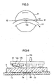
- FIG. 5 is an illustration showing a manner as to how the back surface of the wafer 9 is grinded.
- a rotating grinding wheel (grinding means) 12 is contacted with a grinding surface of the wafer 9, and the grinding surface is grinded in a rotating direction 13 of the grinding wheel 12.
- the grinding site is shifted from one to another by rotating the wafer 9 around an axis of rotation 13a thereof.
- the entirety of the grinding surface of the wafer 9 is grinded.
- FIG. 6 is a cross-sectional view taken along the line VI-VI in FIG. 5 .
- the grinding wheel 12 is arranged as shown in FIG. 6 to be contacted with a substantially half region on the grinding surface of the wafer 9.
- whorl-like grooves 5 are formed in the wafer 9 around an axis of rotation 13a of the wafer 9.
- each surface acoustic wave filter obtained by dividing the wafer 9 into blocks is formed with curved grooves 5 having a feature that the interval of the adjoining grooves 5 is increased, as each groove 5 extends from one end of the wafer 9 (from the axis of rotation 13a of the wafer 9) toward the other end thereof (toward the outermost perimeter of the wafer 9).
- an angle defined by the groove 5 in a region enclosed by a dashed line 15, and the propagating direction 6 of the surface acoustic wave 3 is different from an angle defined by the groove 5 in a region enclosed by a dashed line 16, and the propagating direction 6 of the surface acoustic wave 3. Accordingly, suppressing effect of the unnecessary wave 4 may be varied from site to site in the surface acoustic wave filter.
- wafers 9 are placed on a rotary table 20 rotationally symmetrical to each other for minimizing characteristic variations among surface acoustic wave filters.
- wafers 9a, 9b, 9c, 9d are arranged spaced apart from each other around an axis of rotation 13b of the rotary table 20 equidistantly from the axis of rotation 13b.
- the wafers 9a, 9b, 9c, 9d are arranged at such a position that a linear cutaway portion 30 of each wafer 9b (9c or 9d) is aligned with a cutaway portion 30 of the wafer 9a when the corresponding wafer 9b (9c or 9d) is located at an initial position of the wafer 9a shown in FIG. 8 .
- the grooves 5 have an identical shape among the wafers 9. In this embodiment, described is a case where four pieces of wafers 9 are arranged on the rotary table 20. Alternatively, the number of wafers 9 may be desirably set.
- FIG. 9 is a side view of the rotary table 20, the wafers 9a, 9b, 9c and 9d (9a is not shown), and the grinding wheel 12.
- the rotary table 20 loaded with the plural wafers 9 is rotated around the axis of rotation 13b.
- the grinding wheel 12 is exclusively contacted with the wafer 9b located at a certain spatial position on the rotary table 20 by tilting the grinding wheel 12 relative to the rotating plane of the rotary table 20, or by tilting the rotary table 20 relative to the rotating plane of the grinding wheel 12.
- the wafer 9b is grinded, but the wafer 9d is not grinded.
- the grooves 5 arrayed in predetermined directions as shown in FIG. 8 are formed in each wafer 9a, 9b, 9c, and 9d successively. This arrangement enables to minimize characteristic variations among the surface acoustic wave filters.
- the grinding wheel 12 constituted of plural grinding blades (grinding segments) 12a segmented in the rotating direction of the grinding wheel 12.
- grinding chips can be expelled out of the grinding wheel 12 through clearances 12b each defined by the adjoining grinding blades 12a.
- the grinding blades 12a and the clearances 12b may be arranged regularly or irregularly.
- the length y of the clearance 12b in the rotating direction of the grinding wheel 12 is not smaller than 2.5% and not larger than 50%, and more preferably, not smaller than 5.0% and not larger than 25% relative to the length x of the grinding blade 12a in the rotating direction of the grinding wheel 12 in order to effectively suppress clogging with grinding chips or a like drawback.
- the lengths x and y in the respective ranges, grinding chips can be sufficiently expelled out of the grinding machine, and a stress applied to the wafer 9 can be minimized, thereby preventing crack of the wafer 9.
- the length x of the grinding blade 12a is 20 mm
- the length y of the clearance 12b is 2.5 mm
- the height h of the grinding blade 12a is 4.0 mm.
- the surface roughness of the grinding blade 12a can be varied from each other depending on the depth d of the groove 5 to be formed.
- the depth d of the groove 5 is increased, as the surface roughness of the grinding blade 12a is varied from #2000 to #1500 and then to #1200.
- the depth dof the groove 5 can be varied by preparing grinding blades 12a having at least two different surface roughness from each other and by varying the surface roughness of the grinding blade 12a orderly.
- the surface roughness may be changed alternately, e.g., in the order of #2000, #1500, #2000, #1500, and so on.
- the grinding blades 12a may be arranged in such a manner that a certain number of grinding blades 12a of the same surface roughness are arranged in a group, and the surface roughness is varied alternately group by group, e.g., in the order of #2000, #2000, #1500, #1500, #2000, #2000, and so on.
- the depths of the grooves 5 to be formed in the back surface of the piezoelectric substrate 1 can be varied from each other.
- the grinding blades 12a having three or more different surface roughness are arranged, and the grinding blades 12a having the different surface roughness are disposed adjacent to each other, preferably, the grinding blades 12a are arranged in such a manner that the surface roughness of a certain grinding blade 12a is larger or smaller than the surface roughness of the adjacent grinding blade 12a stepwise, e.g., in the order of #2000, #1500, #1200, #1500, #2000, and so on.
- the grinding blades 12a having at least two different surface roughness are arranged orderly, for instance, in the order of #2000, #1500, #1200, #1500, #2000, #1500, #1200, #1500, #2000, and so on.
- a certain number of grinding blades 12a having the same surface roughness are arranged adjacent to each other in a group, e.g., in the order of #2000, #1500, #1500, #1200, #1500, #1500, #2000, #1500, #1500, #1200, #1500, #1500, #2000, and so on.
- the order of arranging the grinding blades 12a of different surface roughness, or the number of the grinding blades 12a which have the same surface roughness and are disposed adjacent to each other may be optionally set. Any of the above arrangements enables to vary the depth dof the groove 5 while minimizing a stress applied to the wafer 9, and accordingly, adverse effects of the unnecessary wave 4 can be effectively suppressed.
- the rotating numbers of the rotary table 20 and the grinding wheel 12 per unit time, and the surface roughness of the grinding blades 12a are controlled in such a manner that the maximum pitch of the adjoining grooves 5 among the grooves 5 of the wafer 9 is not smaller than 10% and not larger than 500%, more preferably, not smaller than 100% and not larger than 150% relative to the wavelength of the surface acoustic wave 3 propagating through the piezoelectric substrate 1.
- a thick affected layer is formed in a region 17 (see FIG. 2 ) in a region on the back side of the piezoelectric substrate 1.
- the affected layer 17 is a layer in which crystalline structure of a substrate is modified by a stress applied to a wafer in fabricating a surface acoustic wave filter.
- the unnecessary wave 4 is reflected at random in the affected layer 17. Accordingly, propagation of the unnecessary wave 4 is further suppressed in the affected layer 17.
- the maximum pitch of the adjoining grooves 5 may be varied among the surface acoustic wave filters depending on where the surface acoustic wave filter is formed on the wafer.
- the term "maximum pitch or interval" in the specification indicates a pitch of adjoining grooves in a surface acoustic wave filter which is cut out from the vicinity of the center of the wafer.
- the surface acoustic wave filter has been described as an example of the surface acoustic wave device.
- the invention is applicable to general surface acoustic wave devices in need of suppressing adverse effects of an unnecessary wave propagating in a back surface region of a piezoelectric substrate.
- a surface acoustic wave device is a surface acoustic wave device comprising: a piezoelectric substrate; a comb transducer which is formed on a surface of the piezoelectric substrate; and a plurality of grooves which are formed in a back surface of the piezoelectric substrate in a direction intersecting with a propagating direction of a surface acoustic wave, an interval of the adjoining grooves being decreased as the groove extends from one end of the piezoelectric substrate to the other end thereof.
- the plurality of grooves are formed in the back surface of the piezoelectric substrate. Since the respective grooves extend in the direction intersecting with the propagating direction of the surface acoustic wave, unlike an arrangement that grooves extend substantially parallel with the propagating direction of the surface acoustic wave, the degree of variance of reflection of an unnecessary wave that has been sent from the transmitting electrode of the comb transducer and reached the back surface of the piezoelectric substrate can be increased. Thus, there is no or less likelihood that the unnecessary wave may be received by the receiving electrode of the comb transducer. Thus, the surface acoustic wave device exhibits good device characteristics with less or no noise.
- the grooves are formed in such a manner that the interval of the adjoining grooves is decreased as the groove extends from one end of the surface acoustic wave device toward the other end thereof, wherein the one end and the other end are each located on a side substantially perpendicular to the propagating direction of the surface acoustic wave.
- each of the plurality of grooves is curved.
- reflecting conditions of the unnecessary wave on the respective grooves can be varied from each other.
- each of the plurality of grooves is curved, and all the grooves have curvatures with signs identical to each other.
- each of the plurality of grooves is curved, all the grooves have curvatures with signs identical to each other, and the curvature is increased as the groove extends from the one end of the piezoelectric substrate to the other end thereof.
- the degree of variance of reflection of the unnecessary wave can be increased owing to the different curvatures of the grooves between the one end and the other end on the back surface of the surface acoustic wave device. This arrangement enables to effectively suppress adverse effects of the unnecessary wave.
- each of the plurality of grooves has a depth of not smaller than 0.5% relative to a wavelength of the surface acoustic wave propagating through the piezoelectric substrate.
- a maximum interval of the adjoining grooves among the plurality of grooves is not smaller than 10% and not larger than 500% relative to a wavelength of the surface acoustic wave propagating through the piezoelectric substrate.
- the plurality of grooves have at least two different depths from each other.
- a process for fabricating a surface acoustic wave device is a process for fabricating a surface acoustic wave device provided with a piezoelectric substrate, a comb transducer formed on a surface of the piezoelectric substrate, and a plurality of grooves formed in a back surface of the piezoelectric substrate in a direction intersecting with a propagating direction of a surface acoustic wave, the grooves being formed in such a manner that an interval of the adjoining grooves is decreased as the groove extends from one end of the piezoelectric substrate to the other end thereof, wherein the plurality of grooves being formed by grinding.
- This arrangement enables to increase the degree of variance of reflection of the unnecessary wave on the back surface of the piezoelectric substrate, and realize a surface acoustic wave device capable of effectively suppressing adverse effects of the unnecessary wave. Further, since the grinding technique is employed, a thick affected layer in which crystalline structure of the substrate is modified by a stress applied to the substrate in forming the plurality of grooves is formed in a back side region of the piezoelectric substrate. Since the unnecessary wave is reflected at random in the affected layer, adverse effects of the unnecessary wave can be effectively suppressed.
- At least one comb transducer is formed on a surface of a wafer constituted of a piezoelectric member; said at least one wafer is placed on a rotary table in a state that a back surface of the wafer faces upward, said at least one wafer being arranged in a rotating direction of the rotary table, the rotary table is rotated about an axis of rotation thereof, grinding means is rotated about an axis of rotation thereof, the grinding means being tilted relative to a rotary plane of the rotary table at a predetermined angle in such a manner that the grinding means is contacted with said wafer located at a certain spatial position, whereby a plurality of grooves are formed in the back surface of the wafer.
- the wafer is loaded on the rotary table.
- the wafer is loaded on the rotary table in a state that the surface (back surface) opposite to the surface formed with the comb transducer faces upward.
- the wafers are arranged in the rotating direction of the rotary table. Namely, the wafers each having a linear cutaway portion are arranged on the rotary table in such a manner that the cutaway portion of a target wafer to be processed is disposed at the same position on the rotary table every time the target wafer is located at the predetermined position.
- the grinding means is rotated about the axis of rotation thereof, and is tilted in such a manner as to be contacted with the target wafer located at the predetermined spatial position.
- This arrangement makes it possible to form the grooves having a configuration identical to each other among all the wafers loaded on the rotary table.
- the grinding means includes a plurality of grinding segments segmented in the rotating direction of the grinding means, the adjoining grinding segments being separated from each other by a clearance.
- grinding chips can be expelled out of the grinding means through the clearances each defined by the adjoining grinding segments. Further, in this arrangement, it is possible to perform grinding while running water for cleaning. Thereby, clogging of the clearances with the grinding chips or crack of the grinding means can be avoided, and productivity of the surface acoustic wave devices can be raised.
- a length of the clearance in the rotating direction of the grinding means is not smaller than 2.5% and not larger than 50% relative to a length of the grinding segment in the rotating direction of the grinding means.
- the grinding segment has such a surface roughness as to make a depth of the groove formed in the back surface of the wafer of not smaller than 0.5% relative to a wavelength of a surface acoustic wave propagating through the wafer.
- the grooves having the different depths capable of effectively suppressing adverse effects of the unnecessary wave can be formed in the back surface of the surface acoustic wave device.
- the grooves having the interval capable of effectively suppressing adverse effects of the unnecessary wave can be formed in the back surface of the surface acoustic wave device.
- the grinding segments have at least two different surface roughness from each other.
- this arrangement enables to form the grooves having the different depths capable of greatly varying the reflecting directions of the unnecessary wave, and effectively suppressing adverse effects of the unnecessary wave.
- the grinding segments of the grinding means have at least three different surface roughness including a first surface roughness, a second surface roughness, and a third surface roughness, the surface roughness is increased or decreased stepwise in the order from the first, the second, and the third surface roughness, and the grinding segments are arranged in such a manner that the grinding segment having the first surface roughness and the grinding segment having the second surface roughness are disposed adjacent to each other, or the grinding segment having the second surface roughness and the grinding segment having the third surface roughness are disposed adjacent to each other if the grinding segments having the different surface roughness are disposed adjacent to each other.
- the grooves having the different depths can be formed without exerting an excessive stress to the wafer in the grinding. Accordingly, this arrangement enables to fabricate the surface acoustic wave device capable of effectively suppressing adverse effects of the unnecessary wave, in addition to preventing crack of the wafer.
- the grinding segments having the different surface roughness are arranged orderly.
- this arrangement as compared with a case that grinding segments having different surface roughness are arranged irregularly, a stress to be applied to the wafer can be reduced. Also, in this arrangement, the grooves with the depths thereof being gradually varied can be formed. Accordingly, this arrangement enables to fabricate the surface acoustic wave device capable of effectively suppressing adverse effects of the unnecessary wave in addition to preventing crack of the wafer.
- the surface acoustic wave device of the invention is advantageous in suppressing degradation of characteristics arising from reflection on a back surface of a piezoelectric substrate, and is particularly useful in producing communication apparatuses such as mobile phones in need of high performance.
Landscapes
- Physics & Mathematics (AREA)
- Acoustics & Sound (AREA)
- Engineering & Computer Science (AREA)
- Manufacturing & Machinery (AREA)
- Surface Acoustic Wave Elements And Circuit Networks Thereof (AREA)
Claims (16)
- Akustischeoberflächenwelleneinrichtung mit:einem piezoelektrischen Substrat (1);einem Kammwandler (2a, 2b, 2), der auf einer Oberfläche des piezoelektrischen Substrats gebildet ist; undeiner Vielzahl von Rillen (5), die in einer rückseitigen Oberfläche des piezoelektrischen Substrats in einer Richtung gebildet sind, die sich mit einer Ausbreitungsrichtung einer akustischen Oberflächenwelle schneidet,gekennzeichnet dadurch, dassfür jede Rille ein Abstand der benachbarten Rillen abnimmt, wenn sich die Rille von einem Ende (7) des piezoelektrischen Substrats zu seinem anderen Ende (8) erstreckt, wobei das eine Ende und das andere Ende jeweils auf einer Seite angeordnet sind, die im Wesentlichen senkrecht zu der Ausbreitungsrichtung der akustischen Oberflächenwelle steht.
- Akustischeoberflächenwelleneinrichtung nach Anspruch 1, wobei jede der Vielzahl von Rillen gekrümmt ist.
- Akustischeoberflächenwelleneinrichtung nach Anspruch 2, wobei alle Rillen Krümmungen mit Vorzeichen haben, die identisch zueinander sind.
- Akustischeoberflächenwelleneinrichtung nach Anspruch 3, wobei die Krümmung zunimmt, wenn sich die Rille von dem einen Ende des piezoelektrischen Substrats zu dem anderen Ende davon erstreckt.
- Akustischeoberflächenwelleneinrichtung nach Anspruch 1, wobei jede der Vielzahl von Rillen eine Tiefe von nicht weniger als 0,5% einer Wellenlänge der akustischen Oberflächenwelle hat, die sich durch das piezoelektrische Substrat ausbreitet.
- Akustischeoberflächenwelleneinrichtung nach Anspruch 1, wobei ein maximaler Abstand von den benachbarten Rillen unter der Vielzahl von Rillen nicht kleiner als 10% und nicht größer als 500% einer Wellenlänge der akustischen Oberflächenwelle ist, die sich durch das piezoelektrische Substrat ausbreitet.
- Akustischeoberflächenwelleneinrichtung nach Anspruch 1, wobei die Vielzahl von Rillen zumindest zwei voneinander verschiedene Tiefen hat.
- Verfahren zum Herstellen einer Akustischeoberflächenwelleneinrichtung mit einem piezoelektrischen Substrat (1), einem Kammwandler (2a, 2b), der auf einer Oberfläche des piezoelektrischen Substrats gebildet ist, und einer Vielzahl von Rillen (5), die in einer rückseitigen Oberfläche des piezoelektrischen Substrats in einer Richtung gebildet sind, die sich mit einer Ausbreitungsrichtung einer akustischen Oberflächenwelle schneidet, dadurch gekennzeichnet, dass
die Vielzahl von Rillen durch Schleifen gebildet wird,
die Rillen so geformt werden, dass für jede Rille ein Abstand zu den benachbarten Rillen abnimmt, wenn sich die Rille von einem Ende des piezoelektrischen Substrats zu seinem anderen Ende erstreckt, wobei sowohl das eine Ende als auch das andere Ende auf jeweils einer Seite angeordnet sind, die im Wesentlichen senkrecht zu der Ausbreitungsrichtung der akustischen Oberflächenwelle steht. - Herstellverfahren nach Anspruch 8, wobei zumindest ein Kammwandler (2a, 2b, 2) auf einer Oberfläche eines Wafers (9) gebildet wird, der ein piezoelektrisches Bauteil enthält;
der zumindest eine Wafer (9) auf einem drehbaren Tisch in einem Zustand platziert wird, dass eine rückseitige Oberfläche des Wafers nach oben zeigt, wobei der zumindest eine Wafer in einer Rotationsrichtung des drehbaren Tischs angeordnet ist,
der drehbare Tisch um seine Rotationsachse gedreht wird,
eine Schleifeinrichtung (12) um ihre Rotationsachse rotiert wird, wobei die Schleifeinrichtung relativ zu einer Drehebene des drehbaren Tischs um einen vorbestimmten Winkel in so einer Weise gekippt wird, dass die Schleifeinrichtung mit dem Wafer an einer bestimmten räumlichen Position in Kontakt steht, wodurch eine Vielzahl von Rillen in der rückseitigen Oberfläche des Wafers gebildet wird. - Herstellverfahren nach Anspruch 9, wobei die Schleifeinrichtung eine Vielzahl von Schleifsegmenten enthält, die in der Rotationsrichtung der Schleifeinrichtung segmentiert sind, wobei die benachbarten Schleifsegmente voneinander durch eine Lücke getrennt sind.
- Herstellverfahren nach Anspruch 10, wobei eine Länge der Lücke in der Rotationsrichtung der Schleifeinrichtung nicht kleiner als 2,5% und nicht größer als 50% einer Länge des Schleifsegments in der Rotationsrichtung der Schleifeinrichtung ist.
- Herstellverfahren nach Anspruch 10, wobei das Schleifsegment so eine Oberflächenrauheit hat, dass es eine Tiefe der in der rückwärtigen Oberfläche des Wafers gebildeten Rille nicht kleiner als 0,5% einer Wellenlänge einer akustischen Oberflächenwelle macht, die sich durch den Wafer ausbreitet.
- Herstellverfahren nach Anspruch 10, wobei jeweilige Rotationszahlen des drehbaren Tischs und der Schleifeinrichtung pro Einheitszeit und eine Oberflächenrauheit des Schleifsegments in so einer Weise gesteuert werden, dass ein maximaler Abstand der benachbarten Rillen unter der Vielzahl von Rillen nicht kleiner als 10% und nicht größer als 500% einer Wellenlänge einer akustischen Oberflächenwellenlänge ist, die sich durch den Wafer ausbreitet.
- Herstellverfahren nach Anspruch 10, wobei die Schleifsegmente zumindest zwei voneinander verschiedene Oberflächenrauheiten haben.
- Herstellverfahren nach Anspruch 14, wobei die Schleifsegmente der Schleifeinrichtung zumindest drei verschiedene Oberflächenrauheiten einschließlich einer ersten Oberflächenrauheit, einer zweiten Oberflächenrauheit und einer dritten Oberflächenrauheit haben, wobei die Oberflächenrauheit stufenweise in der Reihenfolge von der ersten zu der zweiten und der dritten Oberflächenrauheit wächst oder abnimmt, und die Schleifsegmente in so einer Weise angebracht sind, dass das Schleifsegment mit der ersten Oberflächenrauheit und das Schleifsegment mit der zweiten Oberflächenrauheit zueinander benachbart angeordnet sind, oder das Schleifsegment mit der zweiten Oberflächenrauheit und das Schleifsegment mit der dritten Oberflächenrauheit zueinander benachbart angeordnet sind, wenn die Schleifsegmente mit der unterschiedlichen Oberflächenrauheit benachbart zueinander angeordnet werden.
- Herstellverfahren nach Anspruch 15, wobei die Schleifsegmente mit den verschiedenen Oberflächenrauheiten der Reihe nach angebracht sind.
Applications Claiming Priority (4)
| Application Number | Priority Date | Filing Date | Title |
|---|---|---|---|
| JP2004072563 | 2004-03-15 | ||
| JP2004072563 | 2004-03-15 | ||
| JP2004326189A JP2005303980A (ja) | 2004-03-15 | 2004-11-10 | 弾性表面波デバイスおよびその形成方法 |
| JP2004326189 | 2004-11-10 |
Publications (2)
| Publication Number | Publication Date |
|---|---|
| EP1580885A1 EP1580885A1 (de) | 2005-09-28 |
| EP1580885B1 true EP1580885B1 (de) | 2010-11-03 |
Family
ID=34863539
Family Applications (1)
| Application Number | Title | Priority Date | Filing Date |
|---|---|---|---|
| EP05005257A Expired - Lifetime EP1580885B1 (de) | 2004-03-15 | 2005-03-10 | Oberflächenwellenvorrichtung und Prozess zu ihrer Herstellung |
Country Status (6)
| Country | Link |
|---|---|
| US (1) | US7148769B2 (de) |
| EP (1) | EP1580885B1 (de) |
| JP (1) | JP2005303980A (de) |
| KR (1) | KR101089027B1 (de) |
| CN (1) | CN100576736C (de) |
| DE (1) | DE602005024473D1 (de) |
Families Citing this family (29)
| Publication number | Priority date | Publication date | Assignee | Title |
|---|---|---|---|---|
| US9028748B2 (en) * | 2006-02-24 | 2015-05-12 | Nanovibronix Inc | System and method for surface acoustic wave treatment of medical devices |
| DE102007037502B4 (de) * | 2007-08-08 | 2014-04-03 | Epcos Ag | Bauelement mit reduziertem Temperaturgang |
| FR2922696B1 (fr) * | 2007-10-22 | 2010-03-12 | St Microelectronics Sa | Resonateur a ondes de lamb |
| JP2009147914A (ja) * | 2007-11-22 | 2009-07-02 | Panasonic Corp | 弾性波フィルタ及び弾性波デュプレクサ |
| WO2009104438A1 (ja) * | 2008-02-18 | 2009-08-27 | 株式会社 村田製作所 | 弾性波装置及びその製造方法 |
| US7795781B2 (en) * | 2008-04-24 | 2010-09-14 | Avago Technologies Wireless Ip (Singapore) Pte. Ltd. | Bulk acoustic wave resonator with reduced energy loss |
| JP5770100B2 (ja) * | 2008-12-23 | 2015-08-26 | コーニンクレッカ フィリップス エヌ ヴェ | スプリアス音響モード抑制を持つ集積回路及びその製造方法 |
| CN103109350A (zh) * | 2010-09-30 | 2013-05-15 | 飞思卡尔半导体公司 | 处理半导体晶片的方法、半导体晶片以及半导体器件 |
| WO2013115115A1 (ja) * | 2012-02-03 | 2013-08-08 | 株式会社村田製作所 | 弾性表面波素子及びそれを備えた複合モジュール |
| KR101443015B1 (ko) * | 2012-08-17 | 2014-09-22 | 엔지케이 인슐레이터 엘티디 | 복합 기판, 탄성 표면파 디바이스 및 복합 기판의 제조방법 |
| US10020796B2 (en) * | 2015-08-25 | 2018-07-10 | Avago Technologies General Ip (Singapore) Pte. Ltd. | Surface acoustic wave (SAW) resonator |
| US20170063330A1 (en) * | 2015-08-25 | 2017-03-02 | Avago Technologies General Ip (Singapore) Pte. Ltd. | Surface acoustic wave (saw) resonator |
| US10177734B2 (en) | 2015-08-25 | 2019-01-08 | Avago Technologies International Sales Pte. Limited | Surface acoustic wave (SAW) resonator |
| US10469056B2 (en) | 2015-08-25 | 2019-11-05 | Avago Technologies International Sales Pte. Limited | Acoustic filters integrated into single die |
| US10536133B2 (en) | 2016-04-22 | 2020-01-14 | Avago Technologies International Sales Pte. Limited | Composite surface acoustic wave (SAW) device with absorbing layer for suppression of spurious responses |
| US9991870B2 (en) | 2015-08-25 | 2018-06-05 | Avago Technologies General Ip (Singapore) Pte. Ltd. | Surface acoustic wave (SAW) resonator |
| US10090822B2 (en) * | 2015-08-25 | 2018-10-02 | Avago Technologies General Ip (Singapore) Pte. Ltd. | Surface acoustic wave (SAW) resonator |
| US10523178B2 (en) * | 2015-08-25 | 2019-12-31 | Avago Technologies International Sales Pte. Limited | Surface acoustic wave (SAW) resonator |
| US10177735B2 (en) | 2016-02-29 | 2019-01-08 | Avago Technologies International Sales Pte. Limited | Surface acoustic wave (SAW) resonator |
| JP2017224890A (ja) * | 2016-06-13 | 2017-12-21 | 株式会社村田製作所 | 弾性波装置 |
| JP2018037719A (ja) * | 2016-08-29 | 2018-03-08 | 株式会社村田製作所 | 弾性波装置 |
| JP6778584B2 (ja) * | 2016-10-31 | 2020-11-04 | 太陽誘電株式会社 | 弾性波デバイスの製造方法及びウエハの製造方法 |
| CN111919384B (zh) * | 2018-04-03 | 2024-01-30 | 株式会社村田制作所 | 弹性波装置 |
| US11894824B2 (en) * | 2018-08-30 | 2024-02-06 | Skyworks Solutions, Inc. | Laser-marked packaged surface acoustic wave devices |
| DE102019109022A1 (de) * | 2019-04-05 | 2020-10-08 | RF360 Europe GmbH | Akustische-Oberflächenwellen-Resonatoranordnung |
| CN110445475A (zh) * | 2019-07-29 | 2019-11-12 | 日照东讯电子科技有限公司 | 一种高矩形度声表面波滤波器 |
| CN115804009A (zh) * | 2020-07-15 | 2023-03-14 | 株式会社村田制作所 | 弹性波装置 |
| US12407315B2 (en) | 2021-11-08 | 2025-09-02 | Skyworks Solutions, Inc. | Stacked filter package having multiple types of acoustic wave devices |
| KR20250169194A (ko) * | 2023-05-18 | 2025-12-02 | 코르보 유에스, 인크. | 개선된 성능을 위해 saw 공진기의 전극과 인터리브된 압전 트렌치 |
Family Cites Families (13)
| Publication number | Priority date | Publication date | Assignee | Title |
|---|---|---|---|---|
| FR657592A (fr) | 1963-12-24 | 1929-06-06 | Perfectionnements aux conduits de fumée | |
| GB1438777A (en) * | 1973-09-04 | 1976-06-09 | Mullard Ltd | Electromechanical propagation devices and the manufacture thereof |
| CA1089544A (en) * | 1976-11-09 | 1980-11-11 | Sadao Takahashi | Elastic surface wave device |
| JPS56132806A (en) * | 1980-03-22 | 1981-10-17 | Murata Mfg Co Ltd | Elastic surface wave equipment |
| JPS6226619A (ja) * | 1985-07-26 | 1987-02-04 | Tdk Corp | 弾性表面波装置 |
| JPS6240811A (ja) * | 1985-08-17 | 1987-02-21 | Tdk Corp | 弾性表面波装置 |
| JPH03165116A (ja) * | 1989-11-22 | 1991-07-17 | Clarion Co Ltd | 弾性表面波装置 |
| EP0701812A1 (de) | 1994-09-16 | 1996-03-20 | Dow Corning Corporation | Adsorption von Schweissbestandteilen mit einem macroporösem Copolymer |
| JPH0897675A (ja) | 1994-09-28 | 1996-04-12 | Canon Inc | 弾性表面波素子及びその作製方法及びそれを用いた通信装置 |
| DE19626410A1 (de) | 1996-07-01 | 1998-01-08 | Siemens Matsushita Components | Substrat für mit akustischen Oberflächenwellen arbeitende Bauelemente |
| JPH1168496A (ja) * | 1997-08-11 | 1999-03-09 | Toyo Commun Equip Co Ltd | 弾性表面波デバイスの構造及び製造方法 |
| JP2000278090A (ja) * | 1999-01-21 | 2000-10-06 | Hokuriku Electric Ind Co Ltd | 弾性表面波素子とその製造方法 |
| JP2002246876A (ja) * | 2000-12-15 | 2002-08-30 | Toyo Commun Equip Co Ltd | 弾性表面波素子及び弾性表面波デバイス |
-
2004
- 2004-11-10 JP JP2004326189A patent/JP2005303980A/ja active Pending
-
2005
- 2005-03-10 US US11/076,134 patent/US7148769B2/en not_active Expired - Lifetime
- 2005-03-10 EP EP05005257A patent/EP1580885B1/de not_active Expired - Lifetime
- 2005-03-10 DE DE602005024473T patent/DE602005024473D1/de not_active Expired - Lifetime
- 2005-03-14 KR KR1020050020938A patent/KR101089027B1/ko not_active Expired - Lifetime
- 2005-03-15 CN CN200510055049A patent/CN100576736C/zh not_active Expired - Lifetime
Also Published As
| Publication number | Publication date |
|---|---|
| KR101089027B1 (ko) | 2011-12-01 |
| KR20060043603A (ko) | 2006-05-15 |
| US20050200434A1 (en) | 2005-09-15 |
| JP2005303980A (ja) | 2005-10-27 |
| US7148769B2 (en) | 2006-12-12 |
| EP1580885A1 (de) | 2005-09-28 |
| DE602005024473D1 (de) | 2010-12-16 |
| CN100576736C (zh) | 2009-12-30 |
| CN1671048A (zh) | 2005-09-21 |
Similar Documents
| Publication | Publication Date | Title |
|---|---|---|
| EP1580885B1 (de) | Oberflächenwellenvorrichtung und Prozess zu ihrer Herstellung | |
| CN113678372B (zh) | 高阶模式弹性表面波器件 | |
| JP4696419B2 (ja) | 圧電振動子 | |
| JP2003017974A (ja) | 幅方向波動を抑制する薄膜共振器 | |
| JPS58161493A (ja) | リニア・アレー超音波変換器 | |
| KR102254964B1 (ko) | 탄성파 디바이스 | |
| CN112332797B (zh) | 兰姆波谐振器及其制造方法 | |
| CN109103328B (zh) | 一种声表面波芯片及其制作方法 | |
| EP1289134A2 (de) | Akustische Oberflächenwellenvorrichtung | |
| CA1053364A (en) | Surface acoustic wave transmission device and method of manufacturing same | |
| JP3760378B2 (ja) | 端面反射型表面波装置及びその製造方法 | |
| US20090206954A1 (en) | Elastic surface wave device | |
| JP7527912B2 (ja) | 弾性波デバイス、ウエハ、及びウエハの製造方法 | |
| JP2020136783A (ja) | 弾性波デバイス、フィルタおよびマルチプレクサ | |
| CN1351418A (zh) | 表面声波器件及其制造方法 | |
| JPH07263998A (ja) | 端面反射型表面波共振子 | |
| US20030029432A1 (en) | Cutting method for hard, brittle materials | |
| JP4492623B2 (ja) | 弾性表面波デバイスの製造方法 | |
| JP2006286694A (ja) | ダイシング装置およびダイシング方法 | |
| CN117579025B (zh) | 半导体结构及其形成方法 | |
| US20230336148A1 (en) | Acoustic wave device | |
| JP2010251827A (ja) | 弾性表面波素子 | |
| CN111835313B (zh) | Saw滤波器的制造方法和saw滤波器 | |
| CN223514875U (zh) | Saw滤波器 | |
| KR101824529B1 (ko) | 스크라이빙 휠 |
Legal Events
| Date | Code | Title | Description |
|---|---|---|---|
| PUAI | Public reference made under article 153(3) epc to a published international application that has entered the european phase |
Free format text: ORIGINAL CODE: 0009012 |
|
| AK | Designated contracting states |
Kind code of ref document: A1 Designated state(s): AT BE BG CH CY CZ DE DK EE ES FI FR GB GR HU IE IS IT LI LT LU MC NL PL PT RO SE SI SK TR |
|
| AX | Request for extension of the european patent |
Extension state: AL BA HR LV MK YU |
|
| 17P | Request for examination filed |
Effective date: 20051103 |
|
| AKX | Designation fees paid |
Designated state(s): DE FR GB HU |
|
| RAP1 | Party data changed (applicant data changed or rights of an application transferred) |
Owner name: PANASONIC CORPORATION |
|
| 17Q | First examination report despatched |
Effective date: 20090511 |
|
| GRAP | Despatch of communication of intention to grant a patent |
Free format text: ORIGINAL CODE: EPIDOSNIGR1 |
|
| GRAS | Grant fee paid |
Free format text: ORIGINAL CODE: EPIDOSNIGR3 |
|
| GRAA | (expected) grant |
Free format text: ORIGINAL CODE: 0009210 |
|
| AK | Designated contracting states |
Kind code of ref document: B1 Designated state(s): DE FR GB HU |
|
| REG | Reference to a national code |
Ref country code: GB Ref legal event code: FG4D |
|
| REF | Corresponds to: |
Ref document number: 602005024473 Country of ref document: DE Date of ref document: 20101216 Kind code of ref document: P |
|
| PLBE | No opposition filed within time limit |
Free format text: ORIGINAL CODE: 0009261 |
|
| STAA | Information on the status of an ep patent application or granted ep patent |
Free format text: STATUS: NO OPPOSITION FILED WITHIN TIME LIMIT |
|
| 26N | No opposition filed |
Effective date: 20110804 |
|
| REG | Reference to a national code |
Ref country code: DE Ref legal event code: R097 Ref document number: 602005024473 Country of ref document: DE Effective date: 20110804 |
|
| PGFP | Annual fee paid to national office [announced via postgrant information from national office to epo] |
Ref country code: FR Payment date: 20120319 Year of fee payment: 8 |
|
| PGFP | Annual fee paid to national office [announced via postgrant information from national office to epo] |
Ref country code: GB Payment date: 20120307 Year of fee payment: 8 |
|
| PGFP | Annual fee paid to national office [announced via postgrant information from national office to epo] |
Ref country code: DE Payment date: 20130306 Year of fee payment: 9 |
|
| PG25 | Lapsed in a contracting state [announced via postgrant information from national office to epo] |
Ref country code: HU Free format text: LAPSE BECAUSE OF FAILURE TO SUBMIT A TRANSLATION OF THE DESCRIPTION OR TO PAY THE FEE WITHIN THE PRESCRIBED TIME-LIMIT Effective date: 20101103 |
|
| GBPC | Gb: european patent ceased through non-payment of renewal fee |
Effective date: 20130310 |
|
| REG | Reference to a national code |
Ref country code: FR Ref legal event code: ST Effective date: 20131129 |
|
| PG25 | Lapsed in a contracting state [announced via postgrant information from national office to epo] |
Ref country code: GB Free format text: LAPSE BECAUSE OF NON-PAYMENT OF DUE FEES Effective date: 20130310 Ref country code: FR Free format text: LAPSE BECAUSE OF NON-PAYMENT OF DUE FEES Effective date: 20130402 |
|
| REG | Reference to a national code |
Ref country code: DE Ref legal event code: R119 Ref document number: 602005024473 Country of ref document: DE |
|
| REG | Reference to a national code |
Ref country code: DE Ref legal event code: R082 Ref document number: 602005024473 Country of ref document: DE |
|
| REG | Reference to a national code |
Ref country code: DE Ref legal event code: R119 Ref document number: 602005024473 Country of ref document: DE Effective date: 20141001 |
|
| PG25 | Lapsed in a contracting state [announced via postgrant information from national office to epo] |
Ref country code: DE Free format text: LAPSE BECAUSE OF NON-PAYMENT OF DUE FEES Effective date: 20141001 |