EP1579554B1 - Steuerung für dc/dc-wandler - Google Patents
Steuerung für dc/dc-wandler Download PDFInfo
- Publication number
- EP1579554B1 EP1579554B1 EP03768919.7A EP03768919A EP1579554B1 EP 1579554 B1 EP1579554 B1 EP 1579554B1 EP 03768919 A EP03768919 A EP 03768919A EP 1579554 B1 EP1579554 B1 EP 1579554B1
- Authority
- EP
- European Patent Office
- Prior art keywords
- energy storage
- storage element
- time interval
- charge
- current
- Prior art date
- Legal status (The legal status is an assumption and is not a legal conclusion. Google has not performed a legal analysis and makes no representation as to the accuracy of the status listed.)
- Expired - Lifetime
Links
- 238000004146 energy storage Methods 0.000 claims description 65
- 239000003990 capacitor Substances 0.000 claims description 23
- 230000007423 decrease Effects 0.000 claims description 9
- 238000007599 discharging Methods 0.000 claims description 8
- 238000000034 method Methods 0.000 claims description 6
- 238000012544 monitoring process Methods 0.000 claims description 4
- 101100464779 Saccharomyces cerevisiae (strain ATCC 204508 / S288c) CNA1 gene Proteins 0.000 description 9
- 238000010586 diagram Methods 0.000 description 5
- 101100464782 Saccharomyces cerevisiae (strain ATCC 204508 / S288c) CMP2 gene Proteins 0.000 description 3
- 230000003247 decreasing effect Effects 0.000 description 3
- 230000001360 synchronised effect Effects 0.000 description 2
- 230000001934 delay Effects 0.000 description 1
- 238000012986 modification Methods 0.000 description 1
- 230000004048 modification Effects 0.000 description 1
- 230000003071 parasitic effect Effects 0.000 description 1
- 230000001960 triggered effect Effects 0.000 description 1
Images


Classifications
-
- H—ELECTRICITY
- H02—GENERATION; CONVERSION OR DISTRIBUTION OF ELECTRIC POWER
- H02M—APPARATUS FOR CONVERSION BETWEEN AC AND AC, BETWEEN AC AND DC, OR BETWEEN DC AND DC, AND FOR USE WITH MAINS OR SIMILAR POWER SUPPLY SYSTEMS; CONVERSION OF DC OR AC INPUT POWER INTO SURGE OUTPUT POWER; CONTROL OR REGULATION THEREOF
- H02M3/00—Conversion of DC power input into DC power output
- H02M3/02—Conversion of DC power input into DC power output without intermediate conversion into AC
- H02M3/04—Conversion of DC power input into DC power output without intermediate conversion into AC by static converters
- H02M3/10—Conversion of DC power input into DC power output without intermediate conversion into AC by static converters using discharge tubes with control electrode or semiconductor devices with control electrode
- H02M3/145—Conversion of DC power input into DC power output without intermediate conversion into AC by static converters using discharge tubes with control electrode or semiconductor devices with control electrode using devices of a triode or transistor type requiring continuous application of a control signal
- H02M3/155—Conversion of DC power input into DC power output without intermediate conversion into AC by static converters using discharge tubes with control electrode or semiconductor devices with control electrode using devices of a triode or transistor type requiring continuous application of a control signal using semiconductor devices only
- H02M3/156—Conversion of DC power input into DC power output without intermediate conversion into AC by static converters using discharge tubes with control electrode or semiconductor devices with control electrode using devices of a triode or transistor type requiring continuous application of a control signal using semiconductor devices only with automatic control of output voltage or current, e.g. switching regulators
- H02M3/157—Conversion of DC power input into DC power output without intermediate conversion into AC by static converters using discharge tubes with control electrode or semiconductor devices with control electrode using devices of a triode or transistor type requiring continuous application of a control signal using semiconductor devices only with automatic control of output voltage or current, e.g. switching regulators with digital control
-
- H—ELECTRICITY
- H02—GENERATION; CONVERSION OR DISTRIBUTION OF ELECTRIC POWER
- H02M—APPARATUS FOR CONVERSION BETWEEN AC AND AC, BETWEEN AC AND DC, OR BETWEEN DC AND DC, AND FOR USE WITH MAINS OR SIMILAR POWER SUPPLY SYSTEMS; CONVERSION OF DC OR AC INPUT POWER INTO SURGE OUTPUT POWER; CONTROL OR REGULATION THEREOF
- H02M3/00—Conversion of DC power input into DC power output
- H02M3/02—Conversion of DC power input into DC power output without intermediate conversion into AC
- H02M3/04—Conversion of DC power input into DC power output without intermediate conversion into AC by static converters
- H02M3/10—Conversion of DC power input into DC power output without intermediate conversion into AC by static converters using discharge tubes with control electrode or semiconductor devices with control electrode
- H02M3/145—Conversion of DC power input into DC power output without intermediate conversion into AC by static converters using discharge tubes with control electrode or semiconductor devices with control electrode using devices of a triode or transistor type requiring continuous application of a control signal
- H02M3/155—Conversion of DC power input into DC power output without intermediate conversion into AC by static converters using discharge tubes with control electrode or semiconductor devices with control electrode using devices of a triode or transistor type requiring continuous application of a control signal using semiconductor devices only
- H02M3/156—Conversion of DC power input into DC power output without intermediate conversion into AC by static converters using discharge tubes with control electrode or semiconductor devices with control electrode using devices of a triode or transistor type requiring continuous application of a control signal using semiconductor devices only with automatic control of output voltage or current, e.g. switching regulators
- H02M3/158—Conversion of DC power input into DC power output without intermediate conversion into AC by static converters using discharge tubes with control electrode or semiconductor devices with control electrode using devices of a triode or transistor type requiring continuous application of a control signal using semiconductor devices only with automatic control of output voltage or current, e.g. switching regulators including plural semiconductor devices as final control devices for a single load
- H02M3/1582—Buck-boost converters
-
- H—ELECTRICITY
- H02—GENERATION; CONVERSION OR DISTRIBUTION OF ELECTRIC POWER
- H02M—APPARATUS FOR CONVERSION BETWEEN AC AND AC, BETWEEN AC AND DC, OR BETWEEN DC AND DC, AND FOR USE WITH MAINS OR SIMILAR POWER SUPPLY SYSTEMS; CONVERSION OF DC OR AC INPUT POWER INTO SURGE OUTPUT POWER; CONTROL OR REGULATION THEREOF
- H02M3/00—Conversion of DC power input into DC power output
- H02M3/02—Conversion of DC power input into DC power output without intermediate conversion into AC
- H02M3/04—Conversion of DC power input into DC power output without intermediate conversion into AC by static converters
- H02M3/10—Conversion of DC power input into DC power output without intermediate conversion into AC by static converters using discharge tubes with control electrode or semiconductor devices with control electrode
- H02M3/145—Conversion of DC power input into DC power output without intermediate conversion into AC by static converters using discharge tubes with control electrode or semiconductor devices with control electrode using devices of a triode or transistor type requiring continuous application of a control signal
- H02M3/155—Conversion of DC power input into DC power output without intermediate conversion into AC by static converters using discharge tubes with control electrode or semiconductor devices with control electrode using devices of a triode or transistor type requiring continuous application of a control signal using semiconductor devices only
- H02M3/156—Conversion of DC power input into DC power output without intermediate conversion into AC by static converters using discharge tubes with control electrode or semiconductor devices with control electrode using devices of a triode or transistor type requiring continuous application of a control signal using semiconductor devices only with automatic control of output voltage or current, e.g. switching regulators
- H02M3/158—Conversion of DC power input into DC power output without intermediate conversion into AC by static converters using discharge tubes with control electrode or semiconductor devices with control electrode using devices of a triode or transistor type requiring continuous application of a control signal using semiconductor devices only with automatic control of output voltage or current, e.g. switching regulators including plural semiconductor devices as final control devices for a single load
- H02M3/1588—Conversion of DC power input into DC power output without intermediate conversion into AC by static converters using discharge tubes with control electrode or semiconductor devices with control electrode using devices of a triode or transistor type requiring continuous application of a control signal using semiconductor devices only with automatic control of output voltage or current, e.g. switching regulators including plural semiconductor devices as final control devices for a single load comprising at least one synchronous rectifier element
-
- H—ELECTRICITY
- H02—GENERATION; CONVERSION OR DISTRIBUTION OF ELECTRIC POWER
- H02M—APPARATUS FOR CONVERSION BETWEEN AC AND AC, BETWEEN AC AND DC, OR BETWEEN DC AND DC, AND FOR USE WITH MAINS OR SIMILAR POWER SUPPLY SYSTEMS; CONVERSION OF DC OR AC INPUT POWER INTO SURGE OUTPUT POWER; CONTROL OR REGULATION THEREOF
- H02M1/00—Details of apparatus for conversion
- H02M1/0003—Details of control, feedback or regulation circuits
- H02M1/0009—Devices or circuits for detecting current in a converter
-
- H—ELECTRICITY
- H02—GENERATION; CONVERSION OR DISTRIBUTION OF ELECTRIC POWER
- H02M—APPARATUS FOR CONVERSION BETWEEN AC AND AC, BETWEEN AC AND DC, OR BETWEEN DC AND DC, AND FOR USE WITH MAINS OR SIMILAR POWER SUPPLY SYSTEMS; CONVERSION OF DC OR AC INPUT POWER INTO SURGE OUTPUT POWER; CONTROL OR REGULATION THEREOF
- H02M1/00—Details of apparatus for conversion
- H02M1/0003—Details of control, feedback or regulation circuits
- H02M1/0012—Control circuits using digital or numerical techniques
-
- Y—GENERAL TAGGING OF NEW TECHNOLOGICAL DEVELOPMENTS; GENERAL TAGGING OF CROSS-SECTIONAL TECHNOLOGIES SPANNING OVER SEVERAL SECTIONS OF THE IPC; TECHNICAL SUBJECTS COVERED BY FORMER USPC CROSS-REFERENCE ART COLLECTIONS [XRACs] AND DIGESTS
- Y02—TECHNOLOGIES OR APPLICATIONS FOR MITIGATION OR ADAPTATION AGAINST CLIMATE CHANGE
- Y02B—CLIMATE CHANGE MITIGATION TECHNOLOGIES RELATED TO BUILDINGS, e.g. HOUSING, HOUSE APPLIANCES OR RELATED END-USER APPLICATIONS
- Y02B70/00—Technologies for an efficient end-user side electric power management and consumption
- Y02B70/10—Technologies improving the efficiency by using switched-mode power supplies [SMPS], i.e. efficient power electronics conversion e.g. power factor correction or reduction of losses in power supplies or efficient standby modes
Definitions
- the present invention relates controllers for DC to DC converters and in particular to controllers for controlling inductor current levels without directly measuring such current levels.
- DC to DC converters are used to convert an input DC voltage to an output DC voltage. Such converters may step down (buck) or step up (boost) the input DC voltage.
- One type of buck converter is a synchronous buck converter. This converter typically has a controller, driver, a pair of switches, and an LC filter coupled to the pair of switches. The controller provides a control signal to the driver which then drives the pair of switches, e.g., a high side switch and a low side switch. The driver alternately turns each switch ON and OFF thereby controlling inductor current and the output voltage of the DC to DC converter.
- Such controllers typically utilize a pulse width modulated signal to control the state of the high and low side switches.
- the inductor is coupled to the input voltage source.
- the input voltage is necessarily greater than the output voltage so there is a net positive voltage across the inductor in this switch ON state. Accordingly, the inductor current begins to ramp up.
- the PWM signal is low, the high side switch is OFF and the low side switch is ON. This state of switches will be referred to as a "switch OFF" state. In a buck converter, there is a net negative voltage across the inductor in this state.
- the inductor current begins to ramp down during this low side switch OFF state.
- the pulse width of the PWM signal determines the time on for the switch ON state and the time off for the switch OFF state.
- Such pulse width may be adjusted by directly monitoring the inductor current level via a sense resistor or by comparing the output voltage with a reference voltage level.
- International publication WO 00/16469 refers to a DC to DC converter to convert an input voltage to an output voltage, said DC to DC converter comprising a pair of switches comprising a high side switch and a low side switch, an inductor coupled to said pair of switches, and a controller-configured to estimate a zero crossing of an inductor current through said inductor, wherein said controller is further configured to provide a pulse width modulated (PWM) signal and a low side switch enabling signal.
- PWM pulse width modulated
- Publication US 2002/0074975 A1 refers to a switching DC-to-DC converter including an inductor and a controller which generates at least one power switch control signal or at least one power switch.
- the converter is configured to operate in a continuous mode when the inductor current remains above zero, to enter a discontinuous pulse skipping mode of operation when the inductor current falls to zero and to leave the discontinuous pulse skipping mode and resume continuous mode operation when the inductor current rises above zero.
- the controller includes cycle-skipping circuitry operable in the discontinuous pulse skipping mode and optionally also the continuous mode to cause the power switch to remain off for at least one cycle under the condition that the converter's output potential rises above a threshold.
- the cycle -skipping circuitry includes a comparator which compares an error amplifier output with a threshold potential, and a logic circuitry which asserts a latch-clearing signal once per switching cycle when the comparator output indicates that the converter's output has risen above the threshold.
- a DC to DC converter to convert an input voltage to an output voltage
- said DC to DC converter comprising a pair of switches comprising a high side switch and a low side switch; an inductor coupled to said pair of switches; and a controller configured to estimate a zero crossing of an Inductor current through said inductor, wherein said controller is further configured to provide a pulse width modulated (PWM) signal and a low side switch enabling signal, wherein said high side switch is responsive to said PWM signal and wherein said low side switch is responsive to said PWM signal and said low side switch enabling signal.
- PWM pulse width modulated
- the DC to DC converter according to the invention is characterized by that said controller, comprising an energy storage element, is configured to provide said PWM signal in a digital ON state corresponding to a switch ON state during a first time interval, said controller being further configured to charge said energy storage element during said first time interval and to discharge said energy storage device during a second time interval, wherein the inductor current rises and decreases, respectively, In proportion to the charge on the energy storage element, and wherein said controller is configured to control said first time interval (Ton) to be inversely proportional with said input voltage (Vin) less said output voltage (Vout) by charging said energy storage element (202) during said first time interval (Ton) using a current that is proportional with said input voltage (Vin) less said output voltage (Vout), and by changing the PWM signal to a digital OFF state such that the switches change to the switch OFF state, when the charge on the energy storage element reaches a predetermined charge threshold level.
- said controller comprising an energy storage element, is configured to provide said PWM signal in
- a method of operating a DC to DC converter includes: estimating a zero crossing of an inductor current through an inductor of a DC to DC converter; providing a pulse width modulated (PWM) signal in a digital ON state, a high side switch of said DC to DC converter switching ON in response to said PWM signal in said digital ON state; and determining a first time interval to maintain said PWM signal in said digital ON state.
- PWM pulse width modulated
- the method is characterized by the steps of charging an energy storage element during said first time interval; discharging said energy storage element during a second time interval, wherein the inductor current rises and decreases, respectively, In proportion to the charge on the energy storage element, and controlling said first time interval to be inversely proportional with an input voltage of said DC to DC converter less an output voltage of said DC to DC converter by charging said energy storage element during said first time interval using a current that is proportional with said input voltage less said output voltage, and by changing the PWM signal to a digital OFF state such that the switches change to the switch OFF state, when the charge on the energy storage element reaches a predetermined charge threshold level.
- FIG. 1A illustrates an exemplary DC to DC converter 100 including a controller 102 consistent with the present invention.
- the controller 102 consistent with the invention may be utilized with a variety of DC to DC converters.
- the illustrated DC to DC converter 100 is a synchronous buck converter generally including the controller 102, a driver circuit 104, a pair of switches 106 including a high side switch Q1 and a low side switch Q2, and a low pass filter 108.
- the low pass filter includes an inductor L and a capacitor C.
- the controller 102 is generally configured to provide a PWM signal and a low side switch enable signal (LDR_EN) to the driver circuit 104. Based on such signals, the driver circuit 104 controls the state of the high side switch Q1 and the low side switch Q2.
- LDR_EN low side switch enable signal
- the controller 102 has a target input terminal SLEW where the desired output voltage is set.
- the slew capacitor Cslew charges based on the value of the resistors in the resistor divider R2/R3 and the value of the reference voltage REF.
- the voltage slews from 0 to a set value due to the slew capacitor Cslew.
- An optional sense resistor R1 may be utilized to provide a feedback voltage level to terminals CSN and CSP of the controller 102 representative of the current level through the inductor L.
- terminal VFB of the controller 102 may accept a feedback signal representative of the output voltage level Vout.
- FIG. 1B an exemplary table 120 illustrating various switch states of the high side switch Q1 and the low side switch Q2 of FIG. 1A is illustrated for various PWM and LDR_EN signals.
- the LDR_EN signal is a digital one as in category 122 of the table 120
- the state of the PWM signal controls the switches Q1 and Q2.
- Q1 is ON and Q2 is OFF in this instance 122 if PWM is a digital one. This is referred to as a switch ON state.
- Q1 is OFF and Q2 is ON in this instance 122 if PWM is a digital zero. This is referred to as a switch OFF state.
- Vin is the input voltage to the DC to DC converter
- Vout is the output voltage of the DC to DC converter
- Ton is the time interval duration that the switches Q1 and Q2 are in the switch ON state
- L is the value of the inductor L
- ⁇ I is the change in the inductor current during Ton.
- the voltage across the inductor L is proportional to Vout.
- Vout is the output voltage of the DC to DC converter
- Toff is the time interval duration that the switches Q1 and Q2 are in the switch OFF state
- L is the value of the inductor L
- ⁇ I is the change in the inductor current during Toff.
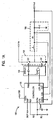
- FIG. 2A a more detailed block diagram of one embodiment of a controller 200 for use with the DC to DC converter of FIG. 1 is illustrated.
- the controller 200 provides a digital one PWM signal to place the switches Q1, Q2 in the switch ON state based on a difference between a first signal representative of the input voltage less a second signal, representative of the output voltage.
- the second signal may be a target voltage level signal, e.g., Vslew, or it may be an output voltage level signal, e.g., Vout.
- use of a target voltage level signal offers smoother current generation.
- the duty cycle of a PWM signal from the controller 200 is generally inversely proportional.to the difference between the input voltage and the output voltage or the target voltage. In other words, as this difference increases, the duty cycle of the PWM signal decreases thereby decreasing the "switch ON" time of the switches Q1 and Q2. Conversely, as the difference between the first signal and second signal decreases, the duty cycle of the PWM signal increases thereby decreasing the "switch OFF" time of the switches Q1 and Q2.
- such control is generally dictated by charging an energy storage element 202 during a first time interval and discharging the energy storage element 202 during a second time interval.
- the PWM output signal is a digital one and hence the switches Q1 and Q2 are in the switch ON state and the inductor current rises in proportion to the charge on the energy storage element 202.
- the PWM signal changes to a digital zero and hence the switches are driven to the switch OFF state. Accordingly, the inductor current then decreases in proportion to the decrease in the charge on the energy storage element 202.
- the controller 200 may generally include various current sources I1, I2, and 13 for charging and discharging the energy storage element 202 based on the results of various voltage comparisons by comparators CMP2, CMP3, and CMP4.
- the first current source 11 is proportional to the output voltage or a target voltage, e.g., Vslew, and configured to provide a first current level
- the second current source 12 is proportional to the input voltage of the DC to DC converter and configured to provide a second current level.
- a third current source 13 is proportional to the output voltage and configured to provide a third current level which is typically, but not necessarily, greater than the first current level.
- the third current source 13 is not mandatory. However, it helps to filter out the parasitic triggering of a new PWM pulse. If the third current source 13 is not utilized, switch S2 can directly discharge the energy storage element 202.
- the controller 200 may also include an output decision circuit 240 to provide the PWM signal to the switch driver circuit.
- the controller 200 may further include a first comparator CMP1 that is configured to compare the charge on the energy storage element 202, e.g., capacitor C1, with a second voltage reference V2.
- the second voltage reference may be a nominal value, e.g., 20 mV in one embodiment, coupled to the positive terminal of the comparator CMP1 such that CMP1 provides a high signal if the charge on the energy storage element is below the nominal V2 value.
- the output of the comparator CMP1 may be further coupled to NAND gate G1.
- a SKIP input may also be coupled to another input of the NAND gage G1. If the SKIP signal is digital zero, then the LDR_EN signal is a digital one regardless of the signal from the comparator CMP1 and hence the PWM signal controls the state of the switches Q1, Q2. If however, SKIP is a digital one and the output from CMP1 is digital one, then the output of NAND gate G1 is a digital zero. As such, if PWM is a digital zero, then both switches Q1 and Q2 will be driven OFF.
- the charge on the energy storage element 202 is initially set at zero volts since it is discharged to ground and the output decision circuit 240 provides a digital zero PWM signal.
- the SLEW voltage will start to increase from zero towards the ratio based on R2 and R3.
- the comparator CMP3 will then sense the SLEW voltage is greater than the feedback voltage VFB, which is representative of the output voltage Vout, and provide a digital one signal to the AND gate G2 of the output decision circuit 240.
- the comparator CMP4 Since there is no current yet through the inductor L, the comparator CMP4 does not sense an over-current condition and provides a digital one signal to the AND gate G2. In addition, since the charge on the energy storage element 202 element has been discharged to zero volts, the output signal of the comparator CMP1 is also a digital one when comparing the charge to the nominal voltage threshold V2. As such, all input signals to the AND gate G2 are a digital one and the flip flop 242 is set. At that moment, the PWM signal goes to a digital one and switch S1 is closed.
- the energy storage element 202 When switch S1 is closed, the energy storage element 202 is charged by a current level equal to the second current level provided by the second current source 12 less the first current level provided by the first current source 11.
- the first current source I1 may provide a first current level representative of the output voltage, e.g., this may be directly proportional to the output voltage level, e.g., Vout, or a target voltage level, e.g., Vslew or Vtarget.
- the energy storage element 202 is charged with a current level proportional to I (Vin - Vout) or (Vin - Vslew).
- the energy storage element 202 is charged until it reaches a predetermined threshold voltage level, e.g., V1 or 2.5 volts in one embodiment.
- the comparator CMP2 compares the charge on the energy storage element 202 with the predetermined threshold voltage level V1 and provides an output signal to the output decision circuit 240 based on the difference. If the charge on the energy storage element 202 reaches the predetermined threshold voltage level V1, then comparator CMP2 will output a digital one signal to the reset terminal R of the flip flop 242 resetting the flip flop so its output Q is moved to a digital zero and hence the PWM signal is also moved to a digital zero.
- switch S1 is open since output Q is a digital zero.
- the energy storage element 202 is now discharged by current source 11.
- An accelerated discharge of the energy storage element 202 may also occur if the output of the AND gate G3 is a digital one. This occurs if the PWM signal is a digital zero hence one input to the AND gate G3 from the QB terminal of the flip flop 242 is a digital one.
- the other input to the AND gate G3 from comparator CMP3 is a digital one if the feedback voltage VFB signal is less than the SLEW voltage. As such, a digital one from the AND gate G3 will close switch S2.
- a third current source 13 may also be coupled to the energy storage element 202 to provide an accelerated discharge.
- the current source 13 has a value of 10 X I_Vout, but its value can be adjusted depending on the particular energy storage element 202 and other parameters to find a desired accelerated discharge level.
- the third current source 13 may be replaced by a short such that switch S2 will discharge the energy storage element to ground.
- the voltage level on the energy storage element 202 will continue to be discharged while the PWM signal is a digital zero. It may be discharged at a normal rate or an accelerated rate depending on a comparison of the SLEW voltage with the feedback voltage VFB as provided by comparator CMP3.
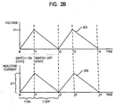
- FIG. 2B a plot 203 of the voltage level on the energy storage element 202 over time is illustrated.
- another plot 205 of the inductor current level in inductor L is illustrated over similar time intervals.
- the charge on the energy storage element is zero volts.
- Ton a first time interval or Ton between time t0 and t1 when the PWM output signal is a digital one, the voltage level on the energy storage element 202 rises linearly until the charge level reaches a predetermined charge threshold level V1, e.g., 2.5 volts in one embodiments.
- Ton between time t0 and t1 depends on the difference between a signal representative of the input voltage Vin and a signal representative of the output voltage, e.g., Vout or Vtarget, since the energy storage element 202 is charged during this time interval with a current level equal proportionate to this difference (current source 12 -11).
- V1 is predetermined charge threshold level (2.5 volts in one example) and I (Vin - Vout) is the value of the charging current provided by the difference between the second current source 12 and the first current source 11 when the second current source is directly proportional to Vout.
- the inductor current rises proportionately to the rise in the voltage level of the energy storage element 202.
- the charge level on the energy storage element is decreased due to discharging.
- the inductor current level also decreases over this time period.
- the controller 200 also provides a zero crossing inductor current estimator.
- the skipping mode when enabled uses this fact that for every PWM pulse the starting inductor current is zero and the energy storage element is completely discharged. When the energy storage element is discharged below the nominal value V2, the output of the comparator CMP1 becomes a digital one. If the skipping mode is enabled then LDR_EN is forced to a digital zero through AND gate G1. So when the inductor current crosses zero, the low side switch Q2 will be OFF as well the high side switch Q1. Therefore, the switching side of the inductor L will be left floating.
- the skipping mode is useful for light load conditions because a new PWM cycle will start when the load discharges the energy storage element, thus minimizing the Q1 and Q2 switching and conduction losses.
- FIG. 3 another embodiment of a controller 300 consistent with the invention is illustrated. Similar to the embodiment of FIG. 1A , the controller 300 provides a PWM control signal to an associated driver circuit based on the input voltage to the associated DC to DC converter less a signal representative of the output voltage, e.g., Vout or Vtarget. However, rather than charge and discharge an energy storage element, the controller 300 essentially counts blocks of time and provides the appropriate PWM and LDR_EN signal based on such counts.
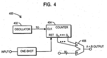
- the controller 300 may generally include an on-time one shot circuit 302, a low side driver one shot circuit 304, a comparator 306, a time delay circuit 308, and a NOR gate 310.
- the time delay circuit 308 may be a blanking circuit for generating retriggering of the on-time one shot circuit 302.
- the one shot circuits 302 and 304 may be triggered by the falling edge of the input signals.
- the on-time for the one shot circuit 302 is proportional to difference between the input voltage Vin of the DC to DC converter and a target voltage Vtarget for the output of the DC to DC converter and T L D R is proportional to Vtarget as detailed in equation (5).
- T L D R is typically chosen to be slightly shorter than suggested by equation (5).
- Ton/T L D R There are several ways to produce Ton/T L D R .
- Vtarget is either a fixed value or one changing in discrete steps.
- Both delays for the one shot circuits 302 and 304 can be digital with the actual delay being a multiple of an elementary time delay, e.g., delay To as given by equations (6) and (7) below.
- Ton To ⁇ 1 * M
- T L D R To ⁇ 2 * N
- the delay circuit 400 generally includes an oscillator 402 for producing time pulses, a counter 404 for counting the time pulses, and a digital comparator 406 for comparing the counted value to an applicable multiple such as M or N.
- the comparator thus provides an output signal indicative of whether or not the counter 404 has reached the necessary amount of counts M or N. Therefore, the applicable on time is controlled by counting the number of counts compared to the multiple M or N.
- Ton is a function of Vin and Vtarget and T L D R is a function of Vtarget
- the multiple N may be produced by a lookup table (LUT) from the digital signal that sets Vtarget.
- the LUT in this instance is one dimensional since various N values correspond to an associated Vtarget value.
- the multiple M may be produced by a LUT from both the digital signal that sets Vtarget and a digitalized Vin signal.
- a digitalized Vin signal may be obtained by utilizing an AD converter on Vin.
- the LUT to produce M in this instance is bi-dimensional since M values correspond to an associated Vtarget and Vin values.
- To1 and To2 are not equal.
- the multiple N is produced similarly as in the first case if To2 is constant.
- the multiple M may be produced by a uni-dimensional LUT having as an input the digital signal that sets Vtarget.
- To1 is not longer fixed but a function of either Vin or a function of both Vin and Vtarget.
Landscapes
- Engineering & Computer Science (AREA)
- Power Engineering (AREA)
- Dc-Dc Converters (AREA)
Claims (8)
- DC/DC-Wandler (100) zum Umwandeln einer Eingangsspannung (Vin) in eine Ausgangsspannung (Vout), wobei der DC/DC-Wandler umfasst:ein Schalterpaar (106), das einen High-Side-Schalter (Q1) und einen Low-Side-Schalter (Q2) umfasst;eine Drossel (L), die mit dem Schalterpaar verbunden ist; und einen Controller (101, 200), der konfiguriert ist für das Schätzen eines Nulldurchgangs eines Drosselstroms durch die Drossel (L), wobei der Controller ferner konfiguriert ist für die Bereitstellung eines impulsbreitenmodulierten (PWM) Signals und eines den Low-Side-Schalter aktivierenden Signals (LDR_EN), wobei der High-Side-Schalter (Q1) auf das PWM-Signal anspricht und wobei der Low-Side-Schalter (Q2) auf das PWM-Signal und auf das den Low-Side-Schalter aktivierende Signal (LDR_EN) anspricht,dadurch gekennzeichnet, dass der Controller, der ein Energiespeicherelement (202) umfasst, derart konfiguriert ist, in einem digitalen AN-Zustand, der einem AN-Zustand des Schalters während eines ersten Zeitintervalls (Ton) entspricht, das PWM-Signal bereitzustellen, wobei der Controller ferner konfiguriert ist für das Laden des Energiespeicherelements (202) während des ersten Zeitintervalls (Ton) und für das Entladen des Energiespeicherelements (202) während eines zweiten Zeitintervalls (Toff), wobei der Drosselstrom im Verhältnis zur Ladung auf dem Energiespeicherelement (202) jeweils zunimmt und abnimmt und wobei die Steuerung konfiguriert ist für ein Steuern des ersten Zeitintervalls (Ton) derart, dass dieses umgekehrt proportional zu der Eingangsspannung (Vin) minus der Ausgangsspannung (Vout) ist, indem das Energiespeicherelement (202) während des ersten Zeitintervalls (Ton) mit einem Strom geladen wird, der proportional ist zu der Eingangsspannung (Vin) minus der Ausgangsspannung (Vout), und indem das PWM-Signal in einen digitalen AUS-Zustand geändert wird, so dass die Schalter (Q1, Q2) in den Schalter-AUS-Zustand wechseln, wenn die Ladung in dem Energiespeicherelement (202) einen vorgegeben Ladezustandschwellwert (V1) erreicht.
- DC/DC-Wandler (100) nach Anspruch 1, wobei das Energiespeicherelement durch einen Kondensator (202) gebildet wird und wobei der Nulldurchgang des Drosselstroms geschätzt wird, indem der Kondensator (202) während des zweiten Zeitintervalls (Toff) unter Verwendung eines zu der Ausgangsspannung (Vout) proportionalen Stroms entladen wird und indem die Ladung des Kondensators (202) auf ein Unterschreiten eines Niedrigspannungsschwellwerts (V2) überwacht wird.
- DC/DC-Wandler (100) nach Anspruch 2, wobei die Schalter High-Side- und Low-Side-Schalter (Q1, Q2) ferner konfiguriert sind für das Schalten eines Schalter-AUS-Zustands, wenn das PWM-Signal digital null und das den Low-Side-Schalter aktivierende Signal (LDR_EN) digital eins ist, wobei die High-Side- und Low-Side-Schalter (Q1, Q2) ferner derart konfiguriert sind, dass beide in einem Sprungzustand auf AUS Schalten, wenn das den Low-Side-Schalter aktivierende Signal (LDR_EN) digital null und das PWM-Signal digital null ist.
- DC/DC-Wandler (100) nach Anspruch 1, wobei die Steuerung (200) umfasst:eine erste Stromquelle (11), die konfiguriert ist für die Bereitstellung eines zur Ausgangsspannung (Vout) proportionalen ersten Strompegels;eine zweite Stromquelle (12), die konfiguriert ist für die Bereitstellung eines zur Eingangsspannung (Vin) proportionalen zweiten Strompegels;wobei das Energiespeicherelement, das durch den Kondensator (202) gebildet wird, derart konfiguriert ist, dass dieses während des ersten Zeitintervalls (Ton) durch einen Ladestrom geladen wird, der gleich dem zweiten Strompegel (12) minus dem ersten Strompegel (11) ist, wobei das erste Zeitintervall (Ton) eine Startzeit (t0) und eine Endzeit (t1) hat, wobei die Startzeit (t0) eintritt, wenn ein Ladezustand des Kondensators (202) im Wesentlichen null ist, und wobei die Endzeit eintritt, wenn ein Ladezustand des Kondensators (202) den Ladezustandschwellwert (V1) übersteigt, wobei der Nulldurchgang des Drosselstroms durch die Startzeit (t0) des ersten Zeitintervalls (Ton) geschätzt wird
- DC/DC-Wandler nach Anspruch 4, wobei die Steuerung (200) während des zweiten Zeitintervalls (Toff) das PWM-Signal in einem digitalen Nullzustand bereitstellt, wobei das zweite Zeitintervall (Toff) eine Startzeit (t1) und eine Endzeit (t2) hat, wobei die Startzeit (t1) des zweiten Zeitintervalls eintritt, wenn ein Ladezustand des Kondensators (202) den Ladezustandschwellwert (V1) übersteigt, und wobei die Endzeit (t2) des zweiten Zeitintervalls eintritt, wenn ein Ladezustand des Kondensators (202) im Wesentlichen null ist, wobei der Nulldurchgang des Drosselstroms durch die Endzeit (t2) des zweiten Zeitintervalls (Toff) geschätzt wird.
- Verfahren, umfassend:das Schätzen eines Nulldurchgangs eines Drosselstroms durch eine Drossel (L) eines DC/DC-Wandlers (100);das Bereitstellen eines impulsbreitenmodulierten (PWM) Signals in einem digitalen AN-Zustand, wobei ein High-Side-Schalter (Q1) des DC/DC-Wandlers (100) in Reaktion auf das PWM-Signal im digitalen AN-Zustand auf AN schaltet; unddas Bestimmen eines ersten Zeitintervalls (Ton), um das PWM-Signal in dem digitalen AN-Zustand zu halten,gekennzeichnet durch die folgenden Schritte:das Laden eines Energiespeicherelements (202) während des ersten Zeitintervalls (Ton);das Entladen des Energiespeicherelements (202) während eines zweiten Zeitintervalls (Toff), wobei sich der Drosselstrom im Verhältnis zur Ladung des Energiespeicherelements (202) jeweils erhöht und verringert, unddas Steuern des ersten Zeitintervalls (Ton) dahingehend, dass dieses umgekehrt proportional zu einer Eingangsspannung (Vin) des DC/DC-Wandlers (100) minus der Ausgangsspannung (Vout) des DC/DC-Wandlers (100) ist, indem das Energiespeicherelement (202) während des ersten Zeitintervalls (Ton) mit einem Strom geladen wird, der proportional zur Eingangsspannung (Vin) minus der Ausgangsspannung (Vout) ist, und indem das PWM-Signal in einen digitalen AUS-Zustand geändert wird, so dass die Schalter (Q1, Q2) in den AUS-Zustand wechseln, wenn die Ladung des Energiespeicherelements (202) einen vorgegebenen Ladezustandschwellwert (V1) erreicht.
- Verfahren nach Anspruch 6, wobei das Energiespeicherelement durch einen Kondensator (202) gebildet wird, wobei der Nulldurchgang des Drosselstroms durch eine Entladung des Kondensators (202) während der zweiten Zeitintervalls (Toff) unter Verwendung eines zur Ausgangsspannung (Vout) proportionalen Stroms und durch eine Überwachung des Ladezustands des Energiespeicherelements (202) eines Controllers (200) für den DC/DC-Wandler (100) geschätzt wird, wobei der Nulldurchgang stattfindet, wenn der Ladezustand des Kondensators (202) einen Niedrigspannungsschwellwert (V2) unterschreitet.
- Verfahren nach Anspruch 6, wobei das Energiespeicherelement durch einen Kondensator (202) gebildet wird, wobei der Nulldurchgang des Drosselstroms durch eine Entladung des Kondensators (202) während der zweiten Zeitintervalls (Toff) unter Verwendung eines zur Ausgangsspannung (Vout) proportionalen Stroms und durch eine Überwachung des Ladezustands des Energiespeicherelements (202) einer Steuerung (200) für den DC/DC-Wandler (100) geschätzt wird, wobei der Nulldurchgang stattfindet, wenn der Ladezustand des Kondensators (202) im Wesentlichen null ist.
Applications Claiming Priority (5)
| Application Number | Priority Date | Filing Date | Title |
|---|---|---|---|
| US42555302P | 2002-11-12 | 2002-11-12 | |
| US425553P | 2002-11-12 | ||
| US10/389,037 US6965221B2 (en) | 2002-11-12 | 2003-03-14 | Controller for DC to DC converter |
| US389037 | 2003-03-14 | ||
| PCT/US2003/036095 WO2004045052A2 (en) | 2002-11-12 | 2003-11-12 | Controller for dc to dc converter |
Publications (3)
| Publication Number | Publication Date |
|---|---|
| EP1579554A2 EP1579554A2 (de) | 2005-09-28 |
| EP1579554A4 EP1579554A4 (de) | 2008-09-03 |
| EP1579554B1 true EP1579554B1 (de) | 2016-01-20 |
Family
ID=32233227
Family Applications (1)
| Application Number | Title | Priority Date | Filing Date |
|---|---|---|---|
| EP03768919.7A Expired - Lifetime EP1579554B1 (de) | 2002-11-12 | 2003-11-12 | Steuerung für dc/dc-wandler |
Country Status (7)
| Country | Link |
|---|---|
| US (3) | US6965221B2 (de) |
| EP (1) | EP1579554B1 (de) |
| JP (1) | JP4291324B2 (de) |
| CN (2) | CN2702526Y (de) |
| AU (1) | AU2003291515A1 (de) |
| TW (1) | TWI238588B (de) |
| WO (1) | WO2004045052A2 (de) |
Families Citing this family (64)
| Publication number | Priority date | Publication date | Assignee | Title |
|---|---|---|---|---|
| US6876181B1 (en) * | 1998-02-27 | 2005-04-05 | Power Integrations, Inc. | Off-line converter with digital control |
| US6844710B2 (en) * | 2002-11-12 | 2005-01-18 | O2Micro International Limited | Controller for DC to DC converter |
| US7075280B2 (en) * | 2003-07-02 | 2006-07-11 | Sigmatel, Inc. | Pulse-skipping PFM DC-DC converter using a voltage mode control loop |
| US6940189B2 (en) * | 2003-07-31 | 2005-09-06 | Andrew Roman Gizara | System and method for integrating a digital core with a switch mode power supply |
| JP4438507B2 (ja) * | 2004-05-12 | 2010-03-24 | セイコーインスツル株式会社 | 電流モード降圧型スイッチングレギュレータ |
| JP4494106B2 (ja) * | 2004-07-14 | 2010-06-30 | 日本電信電話株式会社 | 電源装置、電源制御方法および電源制御プログラム |
| DE102004036958A1 (de) * | 2004-07-30 | 2006-03-23 | Tridonicatco Gmbh & Co. Kg | Ansteuerung von Leistungsschaltern |
| US7081740B2 (en) * | 2004-12-08 | 2006-07-25 | Kiawe Forest, Llc | Digital duty cycle regulator for DC/DC converters |
| JP4311564B2 (ja) * | 2005-03-10 | 2009-08-12 | 富士通マイクロエレクトロニクス株式会社 | 電流モード制御型dc−dcコンバータの制御回路および制御方法 |
| US7233504B2 (en) | 2005-08-26 | 2007-06-19 | Power Integration, Inc. | Method and apparatus for digital control of a switching regulator |
| EP1804368A1 (de) * | 2005-12-29 | 2007-07-04 | Austriamicrosystems AG | Methode zur Gleichstromwandlung and Gleichstromwandleranordnung |
| US7466254B2 (en) | 2006-02-03 | 2008-12-16 | L&L Engineering Llc | Systems and methods for digital control utilizing oversampling |
| US7889019B2 (en) * | 2006-10-13 | 2011-02-15 | Andrew Roman Gizara | Pulse width modulation sequence generating a near critical damped step response |
| US7719336B2 (en) * | 2006-10-31 | 2010-05-18 | Andrew Roman Gizara | Pulse width modulation sequence maintaining maximally flat voltage during current transients |
| US7936087B2 (en) * | 2007-03-12 | 2011-05-03 | System General Corp. | Switching controller for parallel power converters |
| EP2009776A1 (de) * | 2007-06-26 | 2008-12-31 | Austriamicrosystems AG | Auf- und Abwärtstaktregler und zugehöriges Verfahren |
| US8427113B2 (en) * | 2007-08-01 | 2013-04-23 | Intersil Americas LLC | Voltage converter with combined buck converter and capacitive voltage divider |
| US20090033293A1 (en) * | 2007-08-01 | 2009-02-05 | Intersil Americas Inc. | Voltage converter with combined capacitive voltage divider, buck converter and battery charger |
| ATE501545T1 (de) * | 2007-08-20 | 2011-03-15 | Austriamicrosystems Ag | Gleichstromwandleranordnung und verfahren zur gleichstromwandlung |
| US8018212B1 (en) | 2007-08-24 | 2011-09-13 | Intersil Americas Inc. | Buck-boost regulator |
| US8148967B2 (en) * | 2008-08-05 | 2012-04-03 | Intersil Americas Inc. | PWM clock generation system and method to improve transient response of a voltage regulator |
| CN102318174B (zh) * | 2009-02-19 | 2014-06-04 | 皇家飞利浦电子股份有限公司 | 不连续dc-dc电压转换器中的输出电流感测方法 |
| MX350703B (es) | 2009-05-13 | 2017-09-14 | Sio2 Medical Products Inc | Metodo de gasificacion para inspeccionar una superficie revestida. |
| US7985188B2 (en) | 2009-05-13 | 2011-07-26 | Cv Holdings Llc | Vessel, coating, inspection and processing apparatus |
| WO2013170052A1 (en) | 2012-05-09 | 2013-11-14 | Sio2 Medical Products, Inc. | Saccharide protective coating for pharmaceutical package |
| US9458536B2 (en) | 2009-07-02 | 2016-10-04 | Sio2 Medical Products, Inc. | PECVD coating methods for capped syringes, cartridges and other articles |
| US11624115B2 (en) | 2010-05-12 | 2023-04-11 | Sio2 Medical Products, Inc. | Syringe with PECVD lubrication |
| US8450990B2 (en) * | 2010-08-16 | 2013-05-28 | Taiwan Semiconductor Manufacturing Company, Ltd. | Dynamic control loop for switching regulators |
| CN102013820B (zh) * | 2010-10-22 | 2012-07-04 | 凹凸电子(武汉)有限公司 | 交流-直流转换器、方法以及控制器 |
| US8786270B2 (en) | 2010-11-08 | 2014-07-22 | Intersil Americas Inc. | Synthetic ripple regulator with frequency control |
| US9878101B2 (en) | 2010-11-12 | 2018-01-30 | Sio2 Medical Products, Inc. | Cyclic olefin polymer vessels and vessel coating methods |
| US9272095B2 (en) | 2011-04-01 | 2016-03-01 | Sio2 Medical Products, Inc. | Vessels, contact surfaces, and coating and inspection apparatus and methods |
| US11116695B2 (en) | 2011-11-11 | 2021-09-14 | Sio2 Medical Products, Inc. | Blood sample collection tube |
| EP2776603B1 (de) | 2011-11-11 | 2019-03-06 | SiO2 Medical Products, Inc. | Passivierungs-, ph-schutz- oder schmierbeschichtung für arzneimittelverpackung, beschichtungsverfahren und vorrichtung |
| KR101234669B1 (ko) * | 2011-12-08 | 2013-02-19 | 현대자동차주식회사 | 친환경 차량용 dc-dc컨버터의 전류 보상방법 |
| CN102412708B (zh) * | 2011-12-28 | 2014-02-19 | 成都芯源系统有限公司 | 开关变换器及其控制电路和控制方法 |
| US10197607B2 (en) * | 2012-06-26 | 2019-02-05 | City University Of Hong Kong | System and method for estimating component parameters |
| US20150297800A1 (en) | 2012-07-03 | 2015-10-22 | Sio2 Medical Products, Inc. | SiOx BARRIER FOR PHARMACEUTICAL PACKAGE AND COATING PROCESS |
| CA2890066C (en) | 2012-11-01 | 2021-11-09 | Sio2 Medical Products, Inc. | Coating inspection method |
| US9903782B2 (en) | 2012-11-16 | 2018-02-27 | Sio2 Medical Products, Inc. | Method and apparatus for detecting rapid barrier coating integrity characteristics |
| US9764093B2 (en) | 2012-11-30 | 2017-09-19 | Sio2 Medical Products, Inc. | Controlling the uniformity of PECVD deposition |
| JP6382830B2 (ja) | 2012-11-30 | 2018-08-29 | エスアイオーツー・メディカル・プロダクツ・インコーポレイテッド | 医療シリンジ、カートリッジ等上でのpecvd堆積の均一性制御 |
| US9662450B2 (en) | 2013-03-01 | 2017-05-30 | Sio2 Medical Products, Inc. | Plasma or CVD pre-treatment for lubricated pharmaceutical package, coating process and apparatus |
| EP2775600A1 (de) * | 2013-03-04 | 2014-09-10 | Dialog Semiconductor GmbH | Spulenstromabschätzung für ein Schaltnetzteil mit Peakstromsteuerung |
| US9937099B2 (en) | 2013-03-11 | 2018-04-10 | Sio2 Medical Products, Inc. | Trilayer coated pharmaceutical packaging with low oxygen transmission rate |
| EP2971228B1 (de) | 2013-03-11 | 2023-06-21 | Si02 Medical Products, Inc. | Beschichtete verpackung |
| US20160017490A1 (en) | 2013-03-15 | 2016-01-21 | Sio2 Medical Products, Inc. | Coating method |
| EP2804302B1 (de) * | 2013-05-15 | 2017-07-05 | Dialog Semiconductor GmbH | Adaptiver niederleistungs-Nulldurchgangskomparator für ein Schaltnetzteil mit diskontinuierlichem Strommodus |
| US9564817B2 (en) * | 2014-03-17 | 2017-02-07 | Semiconductor Components Industries, Llc | Method and apparatus for dedicated skip mode for resonant converters |
| WO2015148471A1 (en) | 2014-03-28 | 2015-10-01 | Sio2 Medical Products, Inc. | Antistatic coatings for plastic vessels |
| US9864420B2 (en) * | 2014-10-17 | 2018-01-09 | Texas Instruments Deutschland Gmbh | Energy tracking circuit |
| EP3337915B1 (de) | 2015-08-18 | 2021-11-03 | SiO2 Medical Products, Inc. | Pharmazeutische und andere verpackungen mit niedriger sauerstoffübertragungsrate |
| CN107222088B (zh) * | 2016-03-22 | 2019-10-15 | 台达电子工业股份有限公司 | 控制模块、切换式电源供应装置及峰值电流模式控制方法 |
| CN109792202B (zh) * | 2016-10-11 | 2021-05-18 | 阿帕尔斯电力股份有限公司 | 开关模式电源控制器 |
| US10461627B2 (en) | 2018-02-14 | 2019-10-29 | Silanna Asia Pte Ltd | Fractional valley switching controller |
| TWI674740B (zh) * | 2018-06-08 | 2019-10-11 | 茂達電子股份有限公司 | 功率轉換裝置及方法 |
| US10938304B2 (en) * | 2019-06-20 | 2021-03-02 | Intel Corporation | Voltage- and current-based control of direct current (DC)-DC converter |
| EP3772821B1 (de) * | 2019-08-07 | 2025-12-10 | Infineon Technologies AG | Elektrische schaltung, verfahren zur erzeugung eines impulsbreitenmodulierten ausgangssignals und steuerungssystem für eine flugzeitkamera |
| US11005364B1 (en) | 2019-12-18 | 2021-05-11 | Silanna Asia Pte Ltd | Frequency jitter utilizing a fractional valley switching controller |
| TWI729870B (zh) * | 2020-06-29 | 2021-06-01 | 新唐科技股份有限公司 | 恆定功率控制電路 |
| DE102020210577A1 (de) * | 2020-08-20 | 2022-02-24 | Robert Bosch Gesellschaft mit beschränkter Haftung | Verfahren und Vorrichtung zur Ermittlung eines Parameters, wobei der Parameter einen Strom oder eine Spannung in einer Schaltungsanordnung charakterisiert |
| CN114070016B (zh) * | 2021-07-22 | 2024-06-21 | 杰华特微电子股份有限公司 | 开关电路及开关电路的控制方法 |
| US11812234B1 (en) | 2022-03-08 | 2023-11-07 | xMEMS Labs, Inc. | Method of table learning with reduced learning rate applied in driving circuit and driving circuit using the same |
| TWI839141B (zh) * | 2022-03-08 | 2024-04-11 | 美商知微電子有限公司 | 二級反饋控制系統及其相關方法 |
Citations (3)
| Publication number | Priority date | Publication date | Assignee | Title |
|---|---|---|---|---|
| JP2001345682A (ja) * | 2000-06-02 | 2001-12-14 | Koyo Seiko Co Ltd | 三角波発生回路、pwm制御装置及び電動パワーステアリング装置 |
| US6381154B1 (en) * | 2001-03-16 | 2002-04-30 | Tranh To Nguyen | PWM nonlinear controller with a single cycle response and a non resettable integrator |
| KR20020046357A (ko) * | 2000-12-13 | 2002-06-21 | 한흥섭 | 선형적 펄스폭변조 제어장치 |
Family Cites Families (38)
| Publication number | Priority date | Publication date | Assignee | Title |
|---|---|---|---|---|
| JPS61177161A (ja) | 1985-01-30 | 1986-08-08 | Nec Corp | 電源装置 |
| US4727308A (en) * | 1986-08-28 | 1988-02-23 | International Business Machines Corporation | FET power converter with reduced switching loss |
| DE4215980A1 (de) | 1992-05-14 | 1993-11-18 | Siemens Ag | Aktives Freilaufelement |
| US5841362A (en) | 1995-02-10 | 1998-11-24 | Canon Kabushiki Kaisha | Optional apparatus connectable to other apparatus |
| JP3119111B2 (ja) | 1995-04-10 | 2000-12-18 | 株式会社豊田自動織機製作所 | Dc/dcコンバータ |
| JP3097493B2 (ja) | 1995-04-19 | 2000-10-10 | 株式会社豊田自動織機製作所 | Dc/dcコンバータ |
| US5949226A (en) | 1995-04-10 | 1999-09-07 | Kabushiki Kaisha Toyoda Jidoshokki Seisakush | DC/DC converter with reduced power consumpton and improved efficiency |
| JP3090031B2 (ja) | 1995-04-13 | 2000-09-18 | 株式会社豊田自動織機製作所 | Dc/dcコンバータ |
| IT1281349B1 (it) * | 1995-09-19 | 1998-02-18 | Magneti Marelli Spa | Dispositivo regolatore di tensione per alternatore a magneti permanenti |
| JP3402983B2 (ja) | 1997-01-29 | 2003-05-06 | 三洋電機株式会社 | 電源回路 |
| US5905370A (en) * | 1997-05-06 | 1999-05-18 | Fairchild Semiconductor Corporation | Programmable step down DC-DC converter controller |
| US6300777B1 (en) * | 1997-10-15 | 2001-10-09 | International Rectifier Corporation | Lamp ignition detection circuit |
| JP2912346B1 (ja) | 1998-04-08 | 1999-06-28 | 日本電気アイシーマイコンシステム株式会社 | スイッチングレギュレータコントロール回路 |
| US6307356B1 (en) * | 1998-06-18 | 2001-10-23 | Linear Technology Corporation | Voltage mode feedback burst mode circuit |
| JP2000066628A (ja) | 1998-08-21 | 2000-03-03 | Matsushita Electric Ind Co Ltd | Pwm制御システム |
| DE19841341A1 (de) | 1998-09-10 | 2000-03-16 | Bosch Gmbh Robert | Abwärts-Drosselwandler |
| US5982160A (en) * | 1998-12-24 | 1999-11-09 | Harris Corporation | DC-to-DC converter with inductor current sensing and related methods |
| US6137240A (en) * | 1998-12-31 | 2000-10-24 | Lumion Corporation | Universal ballast control circuit |
| JP2000287439A (ja) | 1999-01-26 | 2000-10-13 | Toyota Autom Loom Works Ltd | Dc/dcコンバータおよびその制御回路 |
| EP1095445A1 (de) * | 1999-05-04 | 2001-05-02 | Koninklijke Philips Electronics N.V. | Gleichspannungswandler |
| DE19940419A1 (de) * | 1999-08-26 | 2001-03-08 | Texas Instruments Deutschland | Verfahren zum Betreiben von Aufwärts-Gleichspannungswandlern und Aufwärts-Gleichspannungswandler |
| US6377032B1 (en) * | 2000-07-20 | 2002-04-23 | Semtech Corporation | Method and apparatus for virtual current sensing in DC-DC switched mode power supplies |
| DE10040411A1 (de) * | 2000-08-18 | 2002-03-07 | Infineon Technologies Ag | Schaltungsanordnung mit geregelter Stromaufnahme zur Bereitstellung einer Ausgangsspannung aus einer Eingangsspannung |
| US6396250B1 (en) * | 2000-08-31 | 2002-05-28 | Texas Instruments Incorporated | Control method to reduce body diode conduction and reverse recovery losses |
| US6313616B1 (en) * | 2000-09-21 | 2001-11-06 | Home Touch Lighting Systems Llc | Switching buck converter with floating regulator |
| JP3576526B2 (ja) | 2000-11-21 | 2004-10-13 | ローム株式会社 | Dc/dcコンバータ |
| US6531853B2 (en) | 2000-11-21 | 2003-03-11 | Rohm Co., Ltd. | DC-DC converter |
| US6396252B1 (en) * | 2000-12-14 | 2002-05-28 | National Semiconductor Corporation | Switching DC-to-DC converter with discontinuous pulse skipping and continuous operating modes without external sense resistor |
| US7017087B2 (en) | 2000-12-29 | 2006-03-21 | Teradyne, Inc. | Enhanced loopback testing of serial devices |
| JP2002252979A (ja) | 2001-02-26 | 2002-09-06 | Shindengen Electric Mfg Co Ltd | スイッチング電源 |
| JP2002281744A (ja) | 2001-03-19 | 2002-09-27 | Nec Kansai Ltd | Dc−dcコンバータ |
| JP3637876B2 (ja) | 2001-04-05 | 2005-04-13 | トヨタ自動車株式会社 | Dc−dcコンバータの制御装置 |
| US6366070B1 (en) * | 2001-07-12 | 2002-04-02 | Analog Devices, Inc. | Switching voltage regulator with dual modulation control scheme |
| US6791306B2 (en) | 2002-01-29 | 2004-09-14 | Intersil Americas Inc. | Synthetic ripple regulator |
| US7486894B2 (en) | 2002-06-25 | 2009-02-03 | Finisar Corporation | Transceiver module and integrated circuit with dual eye openers |
| US7203460B2 (en) | 2003-10-10 | 2007-04-10 | Texas Instruments Incorporated | Automated test of receiver sensitivity and receiver jitter tolerance of an integrated circuit |
| US7444558B2 (en) | 2003-12-31 | 2008-10-28 | Intel Corporation | Programmable measurement mode for a serial point to point link |
| US7650540B2 (en) | 2006-07-21 | 2010-01-19 | Intel Corporation | Detecting and differentiating SATA loopback modes |
-
2003
- 2003-03-14 US US10/389,037 patent/US6965221B2/en not_active Expired - Lifetime
- 2003-11-03 TW TW092130622A patent/TWI238588B/zh not_active IP Right Cessation
- 2003-11-12 AU AU2003291515A patent/AU2003291515A1/en not_active Abandoned
- 2003-11-12 WO PCT/US2003/036095 patent/WO2004045052A2/en not_active Ceased
- 2003-11-12 JP JP2005507156A patent/JP4291324B2/ja not_active Expired - Fee Related
- 2003-11-12 EP EP03768919.7A patent/EP1579554B1/de not_active Expired - Lifetime
- 2003-11-12 CN CNU200320100620XU patent/CN2702526Y/zh not_active Expired - Lifetime
- 2003-11-12 CN CN2003101143080A patent/CN1501572B/zh not_active Expired - Fee Related
-
2005
- 2005-11-09 US US11/269,951 patent/US7202650B2/en not_active Expired - Lifetime
-
2007
- 2007-04-10 US US11/733,518 patent/US7598718B2/en not_active Expired - Lifetime
Patent Citations (3)
| Publication number | Priority date | Publication date | Assignee | Title |
|---|---|---|---|---|
| JP2001345682A (ja) * | 2000-06-02 | 2001-12-14 | Koyo Seiko Co Ltd | 三角波発生回路、pwm制御装置及び電動パワーステアリング装置 |
| KR20020046357A (ko) * | 2000-12-13 | 2002-06-21 | 한흥섭 | 선형적 펄스폭변조 제어장치 |
| US6381154B1 (en) * | 2001-03-16 | 2002-04-30 | Tranh To Nguyen | PWM nonlinear controller with a single cycle response and a non resettable integrator |
Also Published As
| Publication number | Publication date |
|---|---|
| JP4291324B2 (ja) | 2009-07-08 |
| EP1579554A4 (de) | 2008-09-03 |
| HK1066639A1 (en) | 2005-03-24 |
| JP2006513690A (ja) | 2006-04-20 |
| CN1501572B (zh) | 2010-05-26 |
| US7202650B2 (en) | 2007-04-10 |
| TW200417115A (en) | 2004-09-01 |
| WO2004045052A3 (en) | 2005-12-29 |
| CN1501572A (zh) | 2004-06-02 |
| TWI238588B (en) | 2005-08-21 |
| US20060061343A1 (en) | 2006-03-23 |
| US20040090804A1 (en) | 2004-05-13 |
| EP1579554A2 (de) | 2005-09-28 |
| US7598718B2 (en) | 2009-10-06 |
| CN2702526Y (zh) | 2005-05-25 |
| AU2003291515A1 (en) | 2004-06-03 |
| US6965221B2 (en) | 2005-11-15 |
| WO2004045052A2 (en) | 2004-05-27 |
| US20070176587A1 (en) | 2007-08-02 |
Similar Documents
| Publication | Publication Date | Title |
|---|---|---|
| EP1579554B1 (de) | Steuerung für dc/dc-wandler | |
| US6844710B2 (en) | Controller for DC to DC converter | |
| US8179105B2 (en) | Systems and methods for controlling output currents of power converters | |
| CN103187854B (zh) | 用于控制电源转换器中的dcm-ccm振荡的系统和方法 | |
| US7161333B2 (en) | System and method for determining load current in switching regulators operable in pulse skipping mode | |
| US20140070785A1 (en) | Controller for a dc to dc converter, a combination of a controller and a dc to dc converter, and a method of operating a dc to dc converter | |
| EP1932236B1 (de) | Schaltregler-tastverhältnisregelung in einem festfrequenzbetrieb | |
| CN102386771A (zh) | 控制器、电流控制方法以及直流直流转换器 | |
| CN119543615A (zh) | 导通时间控制器、电源转换器以及用于其的切换操作方法 | |
| JPH09135568A (ja) | Dc/dcコンバータ | |
| US20250385608A1 (en) | Control unit and method for operating a power converter in a buck-boost mode | |
| US12451805B2 (en) | Feedback current depended ramp generator for switched mode power supply | |
| US20250385607A1 (en) | Control unit and method for transitioning a power converter between a buck mode and a buck-boost mode | |
| US20250385606A1 (en) | Control unit and method for operating a power converter in a boost mode | |
| HK1066639B (en) | Dc/dc converter, controller used for said dc/dc converter, and method for controlling a switch of said dc/dc converter | |
| TW200421699A (en) | Controller for DC to DC converter | |
| HK1117650B (en) | Dc/dc converter | |
| HK1117650A1 (zh) | Dc/dc变换器 | |
| HK1137080B (en) | Method of forming a power supply controller and structure therefor | |
| HK1137080A1 (en) | Method of forming a power supply controller and structure therefor |
Legal Events
| Date | Code | Title | Description |
|---|---|---|---|
| PUAI | Public reference made under article 153(3) epc to a published international application that has entered the european phase |
Free format text: ORIGINAL CODE: 0009012 |
|
| 17P | Request for examination filed |
Effective date: 20050429 |
|
| AK | Designated contracting states |
Kind code of ref document: A2 Designated state(s): AT BE BG CH CY CZ DE DK EE ES FI FR GB GR HU IE IT LI LU MC NL PT RO SE SI SK TR |
|
| AX | Request for extension of the european patent |
Extension state: AL LT LV MK |
|
| PUAK | Availability of information related to the publication of the international search report |
Free format text: ORIGINAL CODE: 0009015 |
|
| RIC1 | Information provided on ipc code assigned before grant |
Ipc: H02M 1/12 20060101AFI20060105BHEP |
|
| DAX | Request for extension of the european patent (deleted) | ||
| A4 | Supplementary search report drawn up and despatched |
Effective date: 20080731 |
|
| RIC1 | Information provided on ipc code assigned before grant |
Ipc: H02M 1/12 20060101AFI20060105BHEP Ipc: H02M 3/156 20060101ALI20080725BHEP |
|
| 17Q | First examination report despatched |
Effective date: 20090115 |
|
| GRAP | Despatch of communication of intention to grant a patent |
Free format text: ORIGINAL CODE: EPIDOSNIGR1 |
|
| INTG | Intention to grant announced |
Effective date: 20150930 |
|
| GRAS | Grant fee paid |
Free format text: ORIGINAL CODE: EPIDOSNIGR3 |
|
| GRAA | (expected) grant |
Free format text: ORIGINAL CODE: 0009210 |
|
| AK | Designated contracting states |
Kind code of ref document: B1 Designated state(s): AT BE BG CH CY CZ DE DK EE ES FI FR GB GR HU IE IT LI LU MC NL PT RO SE SI SK TR |
|
| REG | Reference to a national code |
Ref country code: GB Ref legal event code: FG4D |
|
| REG | Reference to a national code |
Ref country code: CH Ref legal event code: EP |
|
| REG | Reference to a national code |
Ref country code: IE Ref legal event code: FG4D |
|
| REG | Reference to a national code |
Ref country code: AT Ref legal event code: REF Ref document number: 772121 Country of ref document: AT Kind code of ref document: T Effective date: 20160215 |
|
| REG | Reference to a national code |
Ref country code: DE Ref legal event code: R096 Ref document number: 60348497 Country of ref document: DE |
|
| REG | Reference to a national code |
Ref country code: NL Ref legal event code: MP Effective date: 20160120 |
|
| REG | Reference to a national code |
Ref country code: AT Ref legal event code: MK05 Ref document number: 772121 Country of ref document: AT Kind code of ref document: T Effective date: 20160120 |
|
| PG25 | Lapsed in a contracting state [announced via postgrant information from national office to epo] |
Ref country code: NL Free format text: LAPSE BECAUSE OF FAILURE TO SUBMIT A TRANSLATION OF THE DESCRIPTION OR TO PAY THE FEE WITHIN THE PRESCRIBED TIME-LIMIT Effective date: 20160120 |
|
| PG25 | Lapsed in a contracting state [announced via postgrant information from national office to epo] |
Ref country code: ES Free format text: LAPSE BECAUSE OF FAILURE TO SUBMIT A TRANSLATION OF THE DESCRIPTION OR TO PAY THE FEE WITHIN THE PRESCRIBED TIME-LIMIT Effective date: 20160120 Ref country code: GR Free format text: LAPSE BECAUSE OF FAILURE TO SUBMIT A TRANSLATION OF THE DESCRIPTION OR TO PAY THE FEE WITHIN THE PRESCRIBED TIME-LIMIT Effective date: 20160421 Ref country code: FI Free format text: LAPSE BECAUSE OF FAILURE TO SUBMIT A TRANSLATION OF THE DESCRIPTION OR TO PAY THE FEE WITHIN THE PRESCRIBED TIME-LIMIT Effective date: 20160120 Ref country code: IT Free format text: LAPSE BECAUSE OF FAILURE TO SUBMIT A TRANSLATION OF THE DESCRIPTION OR TO PAY THE FEE WITHIN THE PRESCRIBED TIME-LIMIT Effective date: 20160120 |
|
| PG25 | Lapsed in a contracting state [announced via postgrant information from national office to epo] |
Ref country code: AT Free format text: LAPSE BECAUSE OF FAILURE TO SUBMIT A TRANSLATION OF THE DESCRIPTION OR TO PAY THE FEE WITHIN THE PRESCRIBED TIME-LIMIT Effective date: 20160120 Ref country code: PT Free format text: LAPSE BECAUSE OF FAILURE TO SUBMIT A TRANSLATION OF THE DESCRIPTION OR TO PAY THE FEE WITHIN THE PRESCRIBED TIME-LIMIT Effective date: 20160520 Ref country code: SE Free format text: LAPSE BECAUSE OF FAILURE TO SUBMIT A TRANSLATION OF THE DESCRIPTION OR TO PAY THE FEE WITHIN THE PRESCRIBED TIME-LIMIT Effective date: 20160120 |
|
| REG | Reference to a national code |
Ref country code: DE Ref legal event code: R097 Ref document number: 60348497 Country of ref document: DE |
|
| PG25 | Lapsed in a contracting state [announced via postgrant information from national office to epo] |
Ref country code: EE Free format text: LAPSE BECAUSE OF FAILURE TO SUBMIT A TRANSLATION OF THE DESCRIPTION OR TO PAY THE FEE WITHIN THE PRESCRIBED TIME-LIMIT Effective date: 20160120 Ref country code: DK Free format text: LAPSE BECAUSE OF FAILURE TO SUBMIT A TRANSLATION OF THE DESCRIPTION OR TO PAY THE FEE WITHIN THE PRESCRIBED TIME-LIMIT Effective date: 20160120 |
|
| PLBE | No opposition filed within time limit |
Free format text: ORIGINAL CODE: 0009261 |
|
| STAA | Information on the status of an ep patent application or granted ep patent |
Free format text: STATUS: NO OPPOSITION FILED WITHIN TIME LIMIT |
|
| PG25 | Lapsed in a contracting state [announced via postgrant information from national office to epo] |
Ref country code: SK Free format text: LAPSE BECAUSE OF FAILURE TO SUBMIT A TRANSLATION OF THE DESCRIPTION OR TO PAY THE FEE WITHIN THE PRESCRIBED TIME-LIMIT Effective date: 20160120 Ref country code: RO Free format text: LAPSE BECAUSE OF FAILURE TO SUBMIT A TRANSLATION OF THE DESCRIPTION OR TO PAY THE FEE WITHIN THE PRESCRIBED TIME-LIMIT Effective date: 20160120 Ref country code: CZ Free format text: LAPSE BECAUSE OF FAILURE TO SUBMIT A TRANSLATION OF THE DESCRIPTION OR TO PAY THE FEE WITHIN THE PRESCRIBED TIME-LIMIT Effective date: 20160120 |
|
| 26N | No opposition filed |
Effective date: 20161021 |
|
| PG25 | Lapsed in a contracting state [announced via postgrant information from national office to epo] |
Ref country code: BE Free format text: LAPSE BECAUSE OF FAILURE TO SUBMIT A TRANSLATION OF THE DESCRIPTION OR TO PAY THE FEE WITHIN THE PRESCRIBED TIME-LIMIT Effective date: 20160120 |
|
| PG25 | Lapsed in a contracting state [announced via postgrant information from national office to epo] |
Ref country code: SI Free format text: LAPSE BECAUSE OF FAILURE TO SUBMIT A TRANSLATION OF THE DESCRIPTION OR TO PAY THE FEE WITHIN THE PRESCRIBED TIME-LIMIT Effective date: 20160120 Ref country code: BG Free format text: LAPSE BECAUSE OF FAILURE TO SUBMIT A TRANSLATION OF THE DESCRIPTION OR TO PAY THE FEE WITHIN THE PRESCRIBED TIME-LIMIT Effective date: 20160420 |
|
| REG | Reference to a national code |
Ref country code: CH Ref legal event code: PL |
|
| PG25 | Lapsed in a contracting state [announced via postgrant information from national office to epo] |
Ref country code: CH Free format text: LAPSE BECAUSE OF NON-PAYMENT OF DUE FEES Effective date: 20161130 Ref country code: LI Free format text: LAPSE BECAUSE OF NON-PAYMENT OF DUE FEES Effective date: 20161130 |
|
| REG | Reference to a national code |
Ref country code: IE Ref legal event code: MM4A |
|
| REG | Reference to a national code |
Ref country code: FR Ref legal event code: ST Effective date: 20170731 |
|
| PG25 | Lapsed in a contracting state [announced via postgrant information from national office to epo] |
Ref country code: LU Free format text: LAPSE BECAUSE OF NON-PAYMENT OF DUE FEES Effective date: 20161130 |
|
| PG25 | Lapsed in a contracting state [announced via postgrant information from national office to epo] |
Ref country code: FR Free format text: LAPSE BECAUSE OF NON-PAYMENT OF DUE FEES Effective date: 20161130 |
|
| PG25 | Lapsed in a contracting state [announced via postgrant information from national office to epo] |
Ref country code: IE Free format text: LAPSE BECAUSE OF NON-PAYMENT OF DUE FEES Effective date: 20161112 |
|
| PG25 | Lapsed in a contracting state [announced via postgrant information from national office to epo] |
Ref country code: CY Free format text: LAPSE BECAUSE OF FAILURE TO SUBMIT A TRANSLATION OF THE DESCRIPTION OR TO PAY THE FEE WITHIN THE PRESCRIBED TIME-LIMIT Effective date: 20160120 Ref country code: HU Free format text: LAPSE BECAUSE OF FAILURE TO SUBMIT A TRANSLATION OF THE DESCRIPTION OR TO PAY THE FEE WITHIN THE PRESCRIBED TIME-LIMIT; INVALID AB INITIO Effective date: 20031112 |
|
| PG25 | Lapsed in a contracting state [announced via postgrant information from national office to epo] |
Ref country code: TR Free format text: LAPSE BECAUSE OF FAILURE TO SUBMIT A TRANSLATION OF THE DESCRIPTION OR TO PAY THE FEE WITHIN THE PRESCRIBED TIME-LIMIT Effective date: 20160120 Ref country code: MC Free format text: LAPSE BECAUSE OF FAILURE TO SUBMIT A TRANSLATION OF THE DESCRIPTION OR TO PAY THE FEE WITHIN THE PRESCRIBED TIME-LIMIT Effective date: 20160120 |
|
| REG | Reference to a national code |
Ref country code: DE Ref legal event code: R081 Ref document number: 60348497 Country of ref document: DE Owner name: O2MICRO INTERNATIONAL LTD., GEORGE TOWN, KY Free format text: FORMER OWNER: O2MICRO, INC., SANTA CLARA, CALIF., US |
|
| REG | Reference to a national code |
Ref country code: GB Ref legal event code: 732E Free format text: REGISTERED BETWEEN 20220908 AND 20220914 |
|
| PGFP | Annual fee paid to national office [announced via postgrant information from national office to epo] |
Ref country code: GB Payment date: 20221128 Year of fee payment: 20 Ref country code: DE Payment date: 20221125 Year of fee payment: 20 |
|
| REG | Reference to a national code |
Ref country code: DE Ref legal event code: R071 Ref document number: 60348497 Country of ref document: DE |
|
| REG | Reference to a national code |
Ref country code: GB Ref legal event code: PE20 Expiry date: 20231111 |
|
| PG25 | Lapsed in a contracting state [announced via postgrant information from national office to epo] |
Ref country code: GB Free format text: LAPSE BECAUSE OF EXPIRATION OF PROTECTION Effective date: 20231111 |
|
| PG25 | Lapsed in a contracting state [announced via postgrant information from national office to epo] |
Ref country code: GB Free format text: LAPSE BECAUSE OF EXPIRATION OF PROTECTION Effective date: 20231111 |