EP1562237A2 - Dispositif semiconducteur émetteur de lumière à base de nitrure - Google Patents
Dispositif semiconducteur émetteur de lumière à base de nitrure Download PDFInfo
- Publication number
- EP1562237A2 EP1562237A2 EP05250451A EP05250451A EP1562237A2 EP 1562237 A2 EP1562237 A2 EP 1562237A2 EP 05250451 A EP05250451 A EP 05250451A EP 05250451 A EP05250451 A EP 05250451A EP 1562237 A2 EP1562237 A2 EP 1562237A2
- Authority
- EP
- European Patent Office
- Prior art keywords
- nitride
- conductive substrate
- semiconductor element
- layer
- based semiconductor
- Prior art date
- Legal status (The legal status is an assumption and is not a legal conclusion. Google has not performed a legal analysis and makes no representation as to the accuracy of the status listed.)
- Withdrawn
Links
Images


Classifications
-
- H—ELECTRICITY
- H01—ELECTRIC ELEMENTS
- H01L—SEMICONDUCTOR DEVICES NOT COVERED BY CLASS H10
- H01L33/00—Semiconductor devices with at least one potential-jump barrier or surface barrier specially adapted for light emission; Processes or apparatus specially adapted for the manufacture or treatment thereof or of parts thereof; Details thereof
- H01L33/36—Semiconductor devices with at least one potential-jump barrier or surface barrier specially adapted for light emission; Processes or apparatus specially adapted for the manufacture or treatment thereof or of parts thereof; Details thereof characterised by the electrodes
- H01L33/40—Materials therefor
-
- H—ELECTRICITY
- H01—ELECTRIC ELEMENTS
- H01L—SEMICONDUCTOR DEVICES NOT COVERED BY CLASS H10
- H01L33/00—Semiconductor devices with at least one potential-jump barrier or surface barrier specially adapted for light emission; Processes or apparatus specially adapted for the manufacture or treatment thereof or of parts thereof; Details thereof
- H01L33/005—Processes
- H01L33/0093—Wafer bonding; Removal of the growth substrate
-
- H—ELECTRICITY
- H01—ELECTRIC ELEMENTS
- H01L—SEMICONDUCTOR DEVICES NOT COVERED BY CLASS H10
- H01L2933/00—Details relating to devices covered by the group H01L33/00 but not provided for in its subgroups
- H01L2933/0008—Processes
- H01L2933/0016—Processes relating to electrodes
-
- H—ELECTRICITY
- H01—ELECTRIC ELEMENTS
- H01L—SEMICONDUCTOR DEVICES NOT COVERED BY CLASS H10
- H01L33/00—Semiconductor devices with at least one potential-jump barrier or surface barrier specially adapted for light emission; Processes or apparatus specially adapted for the manufacture or treatment thereof or of parts thereof; Details thereof
- H01L33/02—Semiconductor devices with at least one potential-jump barrier or surface barrier specially adapted for light emission; Processes or apparatus specially adapted for the manufacture or treatment thereof or of parts thereof; Details thereof characterised by the semiconductor bodies
- H01L33/26—Materials of the light emitting region
- H01L33/30—Materials of the light emitting region containing only elements of group III and group V of the periodic system
- H01L33/32—Materials of the light emitting region containing only elements of group III and group V of the periodic system containing nitrogen
-
- H—ELECTRICITY
- H01—ELECTRIC ELEMENTS
- H01L—SEMICONDUCTOR DEVICES NOT COVERED BY CLASS H10
- H01L33/00—Semiconductor devices with at least one potential-jump barrier or surface barrier specially adapted for light emission; Processes or apparatus specially adapted for the manufacture or treatment thereof or of parts thereof; Details thereof
- H01L33/36—Semiconductor devices with at least one potential-jump barrier or surface barrier specially adapted for light emission; Processes or apparatus specially adapted for the manufacture or treatment thereof or of parts thereof; Details thereof characterised by the electrodes
- H01L33/38—Semiconductor devices with at least one potential-jump barrier or surface barrier specially adapted for light emission; Processes or apparatus specially adapted for the manufacture or treatment thereof or of parts thereof; Details thereof characterised by the electrodes with a particular shape
-
- H—ELECTRICITY
- H01—ELECTRIC ELEMENTS
- H01L—SEMICONDUCTOR DEVICES NOT COVERED BY CLASS H10
- H01L33/00—Semiconductor devices with at least one potential-jump barrier or surface barrier specially adapted for light emission; Processes or apparatus specially adapted for the manufacture or treatment thereof or of parts thereof; Details thereof
- H01L33/44—Semiconductor devices with at least one potential-jump barrier or surface barrier specially adapted for light emission; Processes or apparatus specially adapted for the manufacture or treatment thereof or of parts thereof; Details thereof characterised by the coatings, e.g. passivation layer or anti-reflective coating
Definitions
- the present invention relates to a nitride-based light-emitting device and a method of manufacturing the same, and more particularly, it relates to a nitride-based light-emitting device comprising a nitride-based semiconductor element layer and a method of manufacturing the same.
- a nitride-based light-emitting device such as a nitride-based light-emitting diode device comprising a nitride-based semiconductor element layer consisting of a nitride-based semiconductor is actively developed at present.
- a nitride-based light-emitting diode device comprising a nitride-based semiconductor element layer consisting of a nitride-based semiconductor is actively developed at present.
- improvement of the light output characteristic of the nitride-based light-emitting diode device and increase of an applied current have recently been developed in particular.
- a nitride-based semiconductor element layer is grown on a sapphire substrate requiring a more reasonable cost than a high-priced nitride-based semiconductor substrate of GaN or the like.
- Fig. 35 is a sectional view showing the structure of a conventional nitride-based light-emitting diode device.
- a buffer layer 102, an underlayer 103, an n-type contact layer 104, an n-type cladding layer 105 and an active layer 106 are successively formed on an insulating sapphire substrate 101 in the conventional nitride-based light-emitting diode device.
- a cap layer 107, a p-type cladding layer 108 and a p-type contact layer 109 are successively formed on the active layer 106.
- the n-type contact layer 104, the n-type cladding layer 105, the active layer 106, the cap layer 107, the p-type cladding layer 108 and the p-type contact layer 109 constitute a nitride-based semiconductor element layer 100.
- the thermal conductivity of the sapphire substrate 101 of the conventional nitride-based light-emitting diode device shown in Fig. 35 is so low that it is disadvantageously difficult to sufficiently radiate heat generated in the nitride-based semiconductor element layer 100.
- a nitride-based light-emitting diode device formed by growing a nitride-based semiconductor element layer on a sapphire substrate and thereafter bonding a cleavable conductive substrate of GaAs or the like to the nitride-based semiconductor element layer and removing the sapphire substrate, as disclosed in Japanese Patent Laying-Open No. 9-8403 (1997), for example.
- a p-side electrode and an n-side electrode can be oppositely arranged through the nitride-based semiconductor element layer due to the employment of the conductive substrate. Therefore, the nitride-based light-emitting diode device may not be assembled by flip chip bonding requiring precise position control dissimilarly to the case of employing the insulating sapphire substrate, whereby the manufacturing yield can be improved.
- a nitride-based light-emitting device comprises a conductive substrate at least containing a single type of metal and a single type of inorganic material having a lower linear expansion coefficient than the metal and a nitride-based semiconductor element layer bonded to the conductive substrate.
- the conductive substrate is so constituted as to contain at least a single type of metal and a single type of inorganic material having a lower linear expansion coefficient than the metal, whereby the conductive substrate can be provided with high thermal conductivity similar to that of the metal.
- the conductive substrate is so employed that two electrodes can be oppositely arranged through the nitride-based semiconductor element layer.
- the emission area can be increased as compared with a nitride-based light-emitting device employing an insulating substrate having two electrodes arranged only on one side of a nitride-based semiconductor element layer, whereby the light output characteristic can be improved.
- the nitride-based light-emitting device may not be assembled by flip chip bonding requiring precise position control for improving the light output characteristic, whereby reduction of the manufacturing yield can be suppressed also by this.
- the inorganic material preferably includes a metal oxide. According to this structure, the linear expansion coefficient of the conductive substrate containing the metal and the inorganic material (metal oxide) can be easily rendered lower than that of a conductive substrate consisting of only a metal.
- the conductive substrate and the nitride-based semiconductor element layer are preferably bonded to each other through the electrode. According to this structure, the conductive substrate and the nitride-based semiconductor element layer can be easily bonded to each other through the electrode.
- a surface of the electrode closer to the nitride-based semiconductor element layer is preferably textured, and the nitride-based semiconductor element layer is preferably formed on the textured surface of the electrode.
- a surface of the conductive substrate closer to the electrode is preferably textured, and the electrode is preferably bonded to the textured surface of the conductive substrate. According to this structure, the contact area between the conductive substrate and the electrode is so increased that heat radiation toward the conductive substrate can be further improved.
- the aforementioned nitride-based light-emitting device preferably further comprises a protective film covering the side surface of the nitride-based semiconductor element layer.
- the protective film can protect the nitride-based semiconductor element layer.
- the inorganic material preferably includes copper oxide. According to this structure, the linear expansion coefficient of the conductive substrate can be easily approached to that of the nitride-based semiconductor element layer through the function of copper oxide, whereby the difference between the linear expansion coefficients of the conductive substrate and the nitride-based semiconductor element layer can be reduced.
- the conductive substrate preferably has thermal conductivity of at least 100 W/m ⁇ K. According to this structure, heat generated in the nitride-based semiconductor element layer can be easily sufficiently radiated toward the conductive substrate. This point has already been experimentally confirmed.
- the conductive substrate preferably has a linear expansion coefficient of not more than 18 ⁇ 10 -6 /K. According to this structure, the difference between the linear expansion coefficients of the conductive substrate and the nitride-based semiconductor element layer can be easily reduced. Thus, the nitride-based light-emitting device can be inhibited from warping resulting from large difference between the linear expansion coefficients of the conductive substrate and the nitride-based semiconductor element layer. This point has also been already experimentally confirmed.
- a method of manufacturing a nitride-based light-emitting device comprises steps of growing a nitride-based semiconductor element layer on a growth substrate, bonding a conductive substrate at least containing a single type of metal and a single type of inorganic material having a lower linear expansion coefficient than the metal to the nitride-based semiconductor element layer and removing the growth substrate from the nitride-based semiconductor element layer to which the conductive substrate is bonded.
- the linear expansion coefficient of the conductive substrate can be approached to that of the nitride-based semiconductor element layer by adjusting the mixing ratio between the metal and the inorganic material through the function of the inorganic material having a low linear expansion coefficient contained in the conductive substrate, whereby the distance between the linear expansion coefficients of the conductive substrate and the nitride-based semiconductor element layer can be reduced.
- the nitride-based light-emitting device can be inhibited from warping or cracking resulting from large difference between the linear expansion coefficients of the conductive substrate and the nitride-based semiconductor element layer in the manufacturing process, whereby reduction of the manufacturing yield can be suppressed.
- the conductive substrate is so employed that two electrodes can be oppositely arranged through the nitride-based semiconductor element layer.
- the emission area can be increased as compared with a nitride-based light-emitting device employing an insulating substrate having two electrodes arranged only on one side of a nitride-based semiconductor element layer, whereby a nitride-based light-emitting device capable of improving the light output characteristic can be formed.
- the nitride-based light-emitting device may not be assembled by flip chip bonding requiring precise position control for improving the light output characteristic, whereby reduction of the manufacturing yield can be suppressed also by this.
- the inorganic material preferably includes a metal oxide. According to this structure, the linear expansion coefficient of the conductive substrate containing the metal and the inorganic material (metal oxide) can be easily rendered lower than that of a conductive substrate consisting of only a metal.
- the step of bonding the conductive substrate to the nitride-based semiconductor element layer preferably includes a step of bonding the conductive substrate to the nitride-based semiconductor element layer through at least either an electrode or a conductive material. According to this structure, the conductive substrate can be easily bonded to the nitride-based semiconductor element layer.
- the step of bonding the conductive substrate to the nitride-based semiconductor element layer preferably includes a step of bonding the conductive substrate to the nitride-based semiconductor element layer through the electrode. According to this structure, the conductive substrate and the nitride-based semiconductor element layer can be easily bonded to each other through the electrode.
- the step of bonding the conductive substrate to the nitride-based semiconductor element layer through the electrode preferably includes steps of texturing a surface of the nitride-based semiconductor element layer, forming the electrode on the textured surface of the nitride-based semiconductor element layer and bonding the conductive substrate to a surface of the electrode opposite to the nitride-based semiconductor element layer.
- this structure light incident upon the interface between the electrode and the nitride-based semiconductor element layer is easily reflected due to the textured surface of the electrode.
- the reflected light is emitted from a surface (light-emitting surface) of the nitride-based semiconductor element layer opposite to the conductive substrate, whereby the light output characteristic can be improved.
- the step of forming the electrode on the textured surface of the nitride-based semiconductor element layer preferably includes a step of forming the electrode on the textured surface of the nitride-based semiconductor element layer to have a textured surface reflecting the texture on the surface of the nitride-based semiconductor element
- the step of bonding the conductive substrate to the surface of the electrode opposite to the nitride-based semiconductor element layer preferably includes steps of texturing a surface of the conductive substrate and bonding the conductive substrate to the surface of the electrode opposite to the nitride-based semiconductor element layer so that the positions of projecting and recess portions of the electrode and the positions of recess and projecting portions of the conductive substrate coincide with each other.
- the contact area between the conductive substrate and the electrode is so increased that heat radiation toward the conductive substrate can be further improved.
- the aforementioned method of manufacturing a nitride-based light-emitting device preferably further comprises a step of forming a protective film to cover the side surface of the nitride-based semiconductor element layer in advance of the step of bonding the conductive substrate to the nitride-based semiconductor element layer.
- the protective film can protect the nitride-based semiconductor element layer.
- the metal may include copper. According to this structure, the conductive substrate can be easily provided with high thermal conductivity similar to that of copper through the function of copper.
- the inorganic material may include copper oxide. According to this structure, the linear expansion coefficient of the conductive substrate can be easily approached to that of the nitride-based semiconductor element layer through the function of copper oxide, whereby the difference between the linear expansion coefficients of the conductive substrate and the nitride-based semiconductor element layer can be reduced.
- the metal may include copper, and the inorganic material may include copper oxide.
- the conductive substrate containing such materials has a linear expansion coefficient close to that of a nitride-based semiconductor such as GaN used for a light-emitting device and high thermal conductivity, whereby warping of the nitride-based light-emitting device resulting from large difference between the linear expansion coefficients of the conductive substrate and the nitride-based semiconductor element layer can be easily suppressed while sufficiently radiating heat generated in the nitride-based semiconductor element layer toward the conductive substrate.
- a nitride-based semiconductor such as GaN used for a light-emitting device and high thermal conductivity
- the conductive substrate may have thermal conductivity of at least 100 W/m ⁇ K. According to this structure, heat generated in the nitride-based semiconductor element layer can be easily sufficiently radiated toward the conductive substrate. This point has already been experimentally confirmed.
- the conductive substrate may have a Young's modulus of not more than 120 GPa. According to this structure, the conductive substrate can be inhibited from deformation under stress.
- the nitride-based semiconductor element layer bonded to the conductive substrate can be inhibited from deformation under stress resulting from deformation under stress of the conductive substrate when the same is separated from the growth substrate. Therefore, the nitride-based semiconductor element layer can be inhibited from cracking, whereby reduction of the manufacturing yield resulting from cracking of the nitride-based light-emitting device can be suppressed. This point has also been already experimentally confirmed.
- the conductive substrate may have a linear expansion coefficient of not more than 18 ⁇ 10 -6 /K. According to this structure, the difference between the linear expansion coefficients of the conductive substrate and the nitride-based semiconductor element layer can be easily reduced. Thus, the nitride-based light-emitting device can be inhibited from cracking resulting from large difference between the linear expansion coefficients of the conductive substrate and the nitride-based semiconductor element layer. This point has also been already experimentally confirmed.
- the p-side electrode 2 prepared by successively forming an Au layer having a thickness of about 100 nm and a Pd layer having a thickness of about 300 nm from the side closer to the conductive substrate 1 is bonded to the conductive substrate 1.
- the p-side electrode 2 is an example of the "electrode" in the present invention.
- An active layer 6 including a well layer of InGaN having a thickness of about 3 nm and a barrier layer of InGaN or GaN having a thickness of about 10 nm is formed on the cap layer 5.
- This active layer 6 has a multiple quantum well (MQW) structure including a plurality of well layers and a plurality of barrier layers or a single quantum well (SQW) structure including a single well layer and a single barrier layer.
- MQW multiple quantum well
- SQW single quantum well
- the p-type contact layer 3, the p-type cladding layer 4, the cap layer 5, the active layer 6, the n-type cladding layer 7 and the n-type contact layer 8 constitute a nitride-based semiconductor element layer 10.
- n-side electrode 9 is formed on a prescribed region of the n-type contact layer 8 constituting the nitride-based semiconductor element layer 10.
- This n-side electrode 9 is constituted of an Al layer having a thickness of about 10 nm, a Pd layer having a thickness of about 10 nm and an Au layer having a thickness of about 100 nm in ascending order.
- the device is separated from an adjacent device along a separation region 10a.
- the separation region 10a may be notched through dicing, for separating the device from the adjacent device along the notch.
- the separation region 10a may be notched through etching, for separating the device from the adjacent device along the notch.
- the separation region 10a of the conductive substrate 1 may be notched through dicing while notching the separation region 10a of the nitride-based semiconductor element layer 10 through etching, for separating the device from the adjacent device along the notches formed through dicing and etching respectively.
- the nitride-based light-emitting diode device according to the first embodiment is formed as shown in Fig. 1.
- a nitride-based light-emitting diode device employs a conductive substrate 21 containing copper and copper oxide mixed with each other at a ratio of 70:30, dissimilarly to the aforementioned first embodiment.
- a p-side electrode 2 having a composition and a thickness similar to those in the aforementioned first embodiment is bonded to the conductive substrate 21 containing copper and copper oxide mixed with each other at the ratio of 70:30, as shown in Fig. 8.
- a nitride-based semiconductor element layer 10 constituted of layers 3 to 8 having compositions and thicknesses similar to those in the aforementioned first embodiment respectively is formed on the p-side electrode 2.
- An n-side electrode 9 having a composition and a thickness similar to those in the aforementioned first embodiment is formed on a prescribed region of the n-type contact layer 8 constituting the nitride-based semiconductor element layer 10.
- the conductive substrate 21 is so formed as to contain copper and copper oxide mixed with each other at the ratio of 70:30, whereby the conductive substrate 21 can be provided with high thermal conductivity similar to that of copper while the linear expansion coefficient of the conductive substrate 21 can be approached to that of the nitride-based semiconductor element layer 10.
- the conductive substrate 21 employed in the second embodiment has a higher percentage of copper and a lower percentage of copper oxide as compared with the conductive substrate 1 containing copper and copper oxide mixed with each other at the ratio of 20:80 in the aforementioned first embodiment. In the conductive substrate 21 employed in the second embodiment, therefore, the thermal conductivity as well as the linear expansion coefficient are higher than those in the conductive substrate 1 employed in the aforementioned first embodiment.
- a nitride-based light-emitting diode device employs a conductive substrate 31 having thermal conductivity of about 170 W/m ⁇ K and containing copper and copper oxide mixed with each other at a ratio of 60:40, dissimilarly to the aforementioned first and second embodiments.
- a p-side electrode 32 having a composition and a thickness similar to those of the p-side electrode 2 in the aforementioned first embodiment with a width smaller than that of the conductive substrate 31 is bonded to the conductive substrate 31 having the thermal conductivity of about 170 W/m ⁇ K and containing copper and copper oxide mixed with each other at the ratio of 60:40, as shown in Fig. 13.
- the p-side electrode 32 is an example of the "electrode" in the present invention.
- a p-type contact layer 33, a p-type cladding layer 34, a cap layer 35, an active layer 36, an n-type cladding layer 37 and an n-type contact layer 38 each having a width smaller than that of the conductive substrate 31 and larger than that of the p-side electrode 32 are successively formed on the p-side electrode 32.
- the p-type contact layer 33, the p-type cladding layer 34, the cap layer 35, the active layer 36, the n-type cladding layer 37 and the n-type contact layer 38 have compositions and thicknesses similar to those of the p-type contact layer 3, the p-type cladding layer 4, the cap layer 5, the active layer 6, the n-type cladding layer 7 and the n-type contact layer 8 in the aforementioned first embodiment respectively.
- the p-type contact layer 33, the p-type cladding layer 34, the cap layer 35, the active layer 36, the n-type cladding layer 37 and the n-type contact layer 38 constitute a nitride-based semiconductor element layer 30.
- a protective film 39 of SiO 2 , SiN, TiO 2 or ZrO having a thickness of about 300 nm is formed to cover regions other than the upper surface of the nitride-based semiconductor element layer 30 (the n-type contact layer 38).
- An n-side electrode 9 having a composition and a thickness similar to those in the aforementioned first embodiment is formed on a prescribed region of the n-type contact layer 38 constituting the nitride-based semiconductor element layer 30.
- a buffer layer 42 and an underlayer 43 are successively grown on an SiC substrate 41 serving as a growth substrate by MOCVD.
- the buffer layer 42 and the underlayer 43 have compositions and thicknesses similar to those of the buffer layer 12 and the underlayer 13 in the aforementioned first embodiment respectively.
- the n-type contact layer 38, the n-type cladding layer 37, the active layer 36, the cap layer 35, the p-type cladding layer 34 and the p-type contact layer 33 are successively grown on the isolation layer 44, and the p-type cladding layer 34 and the p-type contact layer 33 are thereafter converted to the p type.
- a prescribed region of the protective film 39 located on the upper surface of the p-type contact layer 33 constituting the nitride-based semiconductor element layer 30 is removed, and the p-side electrode 32 is thereafter formed on the exposed upper surface of the p-type contact layer 33 by vacuum evaporation or the like.
- the conductive substrate 31 having the thermal conductivity of about 170 W/m ⁇ K and containing copper and copper oxide mixed with each other at the ratio of 60:40 is bonded onto the upper surface of the p-side electrode 32 through a process similar to that of the first embodiment shown in Fig. 4. Thereafter the nitride-based semiconductor element layer 30 located on the isolation layer 44 is isolated from the layers (the SiC substrate 41, the buffer layer 42 and the underlayer 43) located under the isolation layer 44.
- a laser beam is applied through a high-output laser such as a YAG laser, a KrF excimer laser, a DPSS laser (semiconductor laser excited solid-state laser) or a nitrogen laser from the side of the SiC substrate 41, so that the isolation layer 44 absorbs light.
- a high-output laser such as a YAG laser, a KrF excimer laser, a DPSS laser (semiconductor laser excited solid-state laser) or a nitrogen laser from the side of the SiC substrate 41, so that the isolation layer 44 absorbs light.
- the isolation layer 44 is so thermally decomposed as to isolate the nitride-based semiconductor element layer 30 located thereon from the layers (41 to 43) located under the same.
- the isolation layer 44 is made of In 0.5 Ga 0.5 N, and a second harmonic laser beam (wavelength: 532 nm) is applied through a YAG laser from the side of the SiC substrate 41 so that the isolation layer 44 absorbs the laser beam transmitted through the SiC substrate 41, the buffer layer 42 and the underlayer 43.
- a second harmonic laser beam (wavelength: 532 nm) is applied through a YAG laser from the side of the SiC substrate 41 so that the isolation layer 44 absorbs the laser beam transmitted through the SiC substrate 41, the buffer layer 42 and the underlayer 43.
- isolation through the isolation layer 44 can be simplified by properly designing the band gap of the isolation layer 44 and the wavelength of the applied laser beam.
- the isolation layer 44 can most efficiently absorb the laser beam, so that isolation can be easily performed through the isolation layer 44.
- the surface of the n-type contact layer 38 is exposed as shown in Fig. 18.
- the n-side electrode 9 having the composition and the thickness similar to those in the aforementioned first embodiment is formed on the prescribed region of the exposed surface of the n-type contact layer 38 by vacuum evaporation or the like, and the device is separated from an adjacent device along a separation region 30a through a process similar to that of the first embodiment shown in Fig. 7.
- the nitride-based light-emitting diode device according to the third embodiment is formed as shown in Fig. 13.
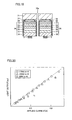
- Fig. 20 shows the relation between the applied currents and the light outputs in the samples of the nitride-based light-emitting diode devices employing the three types of conductive substrates different in thermal conductivity from each other.
- the axis of ordinates shows the light outputs of an arbitrary unit (a.u.)
- the axis of abscissas shows the applied currents (A).
- the light output is increased in proportion to the applied current in the sample of the nitride-based light-emitting diode device according to the third embodiment employing the conductive substrate having the thermal conductivity of about 170 W/m ⁇ K also when the applied current exceeds 1.0 A. It has also been proved that the light output is increased in proportion to the applied current also in the sample of the nitride-based light-emitting diode device employing the conductive substrate having the thermal conductivity of about 100 W/m ⁇ K similarly to the aforementioned sample of the nitride-based light-emitting diode device according to the third embodiment until the applied current reaches a value close to 1.0 A.
- the light output cannot keep proportional relation to the applied current in the sample of the nitride-based light-emitting diode device employing the conductive substrate having the thermal conductivity of about 80 W/m ⁇ K when the applied current exceeds about 0.5 A. It is conceivable from these results that the light output is increased in proportion to the applied current also when the applied current exceeds 0.5 A, if the thermal conductivity of the conductive substrate is at least about 100 W/m ⁇ K.
- the conductive substrate 31 is so formed as to contain copper and copper oxide mixed with each other at the ratio of 60:40, whereby heat generated in the nitride-based semiconductor element layer 30 bonded to the conductive substrate 31 can be easily sufficiently radiated toward the conductive substrate 31 when a high current of at least 0.5 A is fed to the nitride-based light-emitting diode device by setting the thermal conductivity of the conductive substrate 31 to about 170 W/m ⁇ K and hence reduction of the light output characteristic caused by heat can be easily suppressed. Consequently, the nitride-based light-emitting diode device can be provided with a high rated output.
- a p-side electrode 52 having a textured surface with a width smaller than that of the conductive substrate 51 is bonded to the conductive substrate 51 containing copper and copper oxide mixed with each other at the ratio of 45:55, as shown in Fig. 21.
- the p-side electrode 52 has a composition and a thickness similar to those of the p-side electrode 2 in the aforementioned first embodiment.
- the width of portions between the centers of adjacent projecting and recess portions of the textured surface of the p-side electrode 52 is about 0.1 ⁇ m to about 50 ⁇ m, and the height of the projecting portions with reference to the bottoms of the recess portions is about 1 nm to about 2 ⁇ m.
- the p-side electrode 52 is an example of the "electrode" in the present invention.
- a p-type contact layer 53 having a function for serving as a cladding layer is formed on the p-side electrode 52 to fill up the recess portions on the surface of the p-side electrode 52.
- the p-type contact layer 53, the cap layer 54, the active layer 55, the n-type cladding layer 56 and the n-type contact layer 57 constitute a nitride-based semiconductor element layer 50.
- a protective film 58 having a composition and a thickness similar to those of the protective film 39 in the aforementioned third embodiment is formed on the side surfaces of the nitride-based semiconductor element layer 50.
- An n-side electrode 9 having a composition and a thickness similar to those in the aforementioned first embodiment is formed on a prescribed region of the n-type contact layer 57 constituting the nitride-based semiconductor element layer 50.
- a buffer layer 62 and an underlayer 63 are successively grown on an Si substrate 61 serving as a growth substrate by MOCVD.
- the buffer layer 62 and the underlayer 63 have compositions and thicknesses similar to those of the buffer layer 12 and the underlayer 13 in the aforementioned first embodiment respectively.
- the p-type contact layer 57, the n-type cladding layer 56, the active layer 55, the cap layer 54 and the p-type contact layer 53 are successively grown on the underlayer 63, and the p-type contact layer 53 is thereafter converted to the p type.
- a trench having a depth reaching the Si substrate 61 is formed in a separation region 50a by etching, thereby parting the nitride-based semiconductor element layer 50 through the trench.
- the protective film 58 is formed by CVD to cover the nitride-based semiconductor element layer 50, the buffer layer 62 and the underlayer 63.
- the portion of the protective film 58 located on the upper surface of the p-type contact layer 53 is removed, and the exposed surface of the p-type contact layer 53 is thereafter textured by photolithography and dry etching.
- the surface of the p-type contact layer 53 is so textured that the width of the portions between the centers of the adjacent projecting and recess portions of the textured surface of the p-type contact layer 53 is about 0.1 ⁇ m to about 50 ⁇ m and the height of the projecting portions with reference to the bottoms of the recess portions is about 1 nm to about 2 ⁇ m.
- the p-side electrode 52 is formed by vacuum evaporation or the like to fill up the recess portions on the surface of the p-type contact layer 53.
- the n-side electrode 9 having the composition and the thickness similar to those in the aforementioned first embodiment is formed on the prescribed region of the exposed surface of the n-type contact layer 57 by vacuum evaporation or the like, and the device is separated from an adjacent device along the separation region 50a through a process similar to that of the first embodiment shown in Fig. 7.
- the nitride-based light-emitting diode device according to the fourth embodiment is formed as shown in Fig. 21.
- Table 1 shows results of an experiment for investigating presence/absence of cracks on nitride-based semiconductor element layers with reference to five conductive substrates having different Young's moduli (about 100 GPa, about 110 GPa, about 120 GPa, about 130 GPa and about 140 GPa) respectively.
- the Young's moduli of about 100 GPa, about 110 GPa, about 120 GPa, about 130 GPa and about 140 GPa were adjusted by adjusting the mixing ratios of copper and copper oxide contained in the conductive substrates respectively. Further, the Young's moduli of about 130 GPa and about 140 GPa were adjusted by employing other conductive metals. Young's Modulus (GPa) Crack 100 no 110 no 120 no 130 yes 140 yes
- the conductive substrate 51 has the Young's modulus of about 50 GPa, whereby the nitride-based semiconductor element layer 50 can conceivably be inhibited from cracking.
- the surface of the conductive substrate 71 is textured similarly to the textured surfaces of the p-side electrode 72 formed on the p-type contact layer 73 while the conductive substrate 71 and the p-side electrode 72 are so bonded to each other that the positions of the recess portions (projecting portions) of the conductive substrate 71 coincide with the positions of the projecting portions (recess portions) of the p-side electrode 72, whereby the contact area between the conductive substrate 71 and the p-side electrode 72 is increased and heat radiation toward the conductive substrate 71 can be further improved.
- the nitride-based semiconductor element layer includes the layer of GaN, AlGaN or InGaN in each of the aforementioned first to fifth embodiments, the present invention is not restricted to this but the nitride-based semiconductor element layer may alternatively include a layer other than the layer of GaN, AlGaN or InGaN.
Applications Claiming Priority (2)
| Application Number | Priority Date | Filing Date | Title |
|---|---|---|---|
| JP2004030048A JP2005223165A (ja) | 2004-02-06 | 2004-02-06 | 窒化物系発光素子 |
| JP2004030048 | 2004-02-06 |
Publications (2)
| Publication Number | Publication Date |
|---|---|
| EP1562237A2 true EP1562237A2 (fr) | 2005-08-10 |
| EP1562237A3 EP1562237A3 (fr) | 2008-01-16 |
Family
ID=34675540
Family Applications (1)
| Application Number | Title | Priority Date | Filing Date |
|---|---|---|---|
| EP05250451A Withdrawn EP1562237A3 (fr) | 2004-02-06 | 2005-01-28 | Dispositif semiconducteur émetteur de lumière à base de nitrure |
Country Status (4)
| Country | Link |
|---|---|
| US (3) | US7592630B2 (fr) |
| EP (1) | EP1562237A3 (fr) |
| JP (1) | JP2005223165A (fr) |
| CN (2) | CN100524852C (fr) |
Cited By (3)
| Publication number | Priority date | Publication date | Assignee | Title |
|---|---|---|---|---|
| EP2017898A1 (fr) * | 2007-07-17 | 2009-01-21 | Vishay Israel Ltd. | Dispositif semi-conducteur émetteur de lumière et son procédé de fabrication |
| EP2448016A3 (fr) * | 2010-11-01 | 2014-04-09 | Samsung Electronics Co., Ltd. | Procédé de fabrication de dispositif électroluminescent à semi-conducteur |
| EP3107128A4 (fr) * | 2014-03-24 | 2016-12-21 | Shanghai Chiptek Semiconductor Tech Co Ltd | Tranche épitaxiale de del bleue non polaire basée sur un substrat lao et son procédé de préparation |
Families Citing this family (33)
| Publication number | Priority date | Publication date | Assignee | Title |
|---|---|---|---|---|
| CN100372137C (zh) * | 2005-05-27 | 2008-02-27 | 晶能光电(江西)有限公司 | 具有上下电极结构的铟镓铝氮发光器件及其制造方法 |
| KR100635157B1 (ko) | 2005-09-09 | 2006-10-17 | 삼성전기주식회사 | 질화물계 반도체 발광소자 |
| JP4799974B2 (ja) * | 2005-09-16 | 2011-10-26 | 昭和電工株式会社 | 窒化物系半導体発光素子及びその製造方法 |
| JP4799975B2 (ja) * | 2005-09-16 | 2011-10-26 | 昭和電工株式会社 | 窒化物系半導体発光素子及びその製造方法 |
| KR100649763B1 (ko) * | 2005-12-09 | 2006-11-27 | 삼성전기주식회사 | 수직구조 질화물 발광소자의 제조방법 |
| SG10201405004WA (en) * | 2006-02-23 | 2014-10-30 | Azzurro Semiconductors Ag | Nitride semiconductor component and process for its production |
| KR100755658B1 (ko) * | 2006-03-09 | 2007-09-04 | 삼성전기주식회사 | 발광다이오드 패키지 |
| GB2436398B (en) * | 2006-03-23 | 2011-08-24 | Univ Bath | Growth method using nanostructure compliant layers and HVPE for producing high quality compound semiconductor materials |
| JP5232971B2 (ja) * | 2006-04-28 | 2013-07-10 | 豊田合成株式会社 | 窒化物系半導体発光素子の製造方法 |
| JP5113446B2 (ja) * | 2006-08-11 | 2013-01-09 | 三洋電機株式会社 | 半導体素子およびその製造方法 |
| JP5126875B2 (ja) * | 2006-08-11 | 2013-01-23 | シャープ株式会社 | 窒化物半導体発光素子の製造方法 |
| TWI318013B (en) | 2006-09-05 | 2009-12-01 | Epistar Corp | A light emitting device and the manufacture method thereof |
| GB0701069D0 (en) * | 2007-01-19 | 2007-02-28 | Univ Bath | Nanostructure template and production of semiconductors using the template |
| TW200840082A (en) * | 2007-03-22 | 2008-10-01 | Univ Nat Sun Yat Sen | LED structure made of ZnO |
| WO2009004980A1 (fr) * | 2007-06-29 | 2009-01-08 | Showa Denko K.K. | Procédé de fabrication d'une diode électroluminescente |
| TWI411124B (zh) * | 2007-07-10 | 2013-10-01 | Delta Electronics Inc | 發光二極體裝置及其製造方法 |
| US8652947B2 (en) * | 2007-09-26 | 2014-02-18 | Wang Nang Wang | Non-polar III-V nitride semiconductor and growth method |
| US7928448B2 (en) * | 2007-12-04 | 2011-04-19 | Philips Lumileds Lighting Company, Llc | III-nitride light emitting device including porous semiconductor layer |
| US7791101B2 (en) * | 2008-03-28 | 2010-09-07 | Cree, Inc. | Indium gallium nitride-based ohmic contact layers for gallium nitride-based devices |
| WO2009129353A1 (fr) * | 2008-04-15 | 2009-10-22 | Purdue Research Foundation | Substrat en silicium métallisé destiné à une diode électroluminescente au nitrure de gallium enrichi à l’indium |
| JP2010258296A (ja) * | 2009-04-27 | 2010-11-11 | Renesas Electronics Corp | 窒化物系半導体光素子およびその製造方法 |
| TW201112440A (en) * | 2009-09-29 | 2011-04-01 | Ubilux Optoelectronics Corp | Manufacturing method of vertical light emitting diode |
| US8471282B2 (en) * | 2010-06-07 | 2013-06-25 | Koninklijke Philips Electronics N.V. | Passivation for a semiconductor light emitting device |
| KR101735670B1 (ko) * | 2010-07-13 | 2017-05-15 | 엘지이노텍 주식회사 | 발광 소자 |
| TWI429110B (zh) * | 2011-01-07 | 2014-03-01 | Nat Univ Tsing Hua | 具有自我複製式光子晶體之發光元件與其製造方法 |
| KR101781436B1 (ko) | 2011-07-22 | 2017-09-25 | 삼성전자주식회사 | 질화물계 반도체 발광소자 |
| US9343641B2 (en) | 2011-08-02 | 2016-05-17 | Manutius Ip, Inc. | Non-reactive barrier metal for eutectic bonding process |
| JP6066253B2 (ja) * | 2011-09-26 | 2017-01-25 | 東芝ライテック株式会社 | 発光装置の製造方法 |
| US9574135B2 (en) * | 2013-08-22 | 2017-02-21 | Nanoco Technologies Ltd. | Gas phase enhancement of emission color quality in solid state LEDs |
| WO2015118419A1 (fr) * | 2014-02-06 | 2015-08-13 | Koninklijke Philips N.V. | Diode électroluminescente à substrat structuré |
| WO2015156381A1 (fr) * | 2014-04-10 | 2015-10-15 | 富士電機株式会社 | Procédé de traitement de substrat semi-conducteur et procédé de fabrication de dispositif à semi-conducteur mettant en œuvre ledit procédé de traitement |
| KR20170008417A (ko) * | 2015-07-14 | 2017-01-24 | 에스프린팅솔루션 주식회사 | 자동장착장치 및 이를 포함하는 화상형성장치 |
| JP7041338B2 (ja) * | 2017-09-01 | 2022-03-24 | 日亜化学工業株式会社 | 発光装置の製造方法 |
Citations (5)
| Publication number | Priority date | Publication date | Assignee | Title |
|---|---|---|---|---|
| JPH098403A (ja) * | 1995-06-15 | 1997-01-10 | Nichia Chem Ind Ltd | 窒化物半導体素子の製造方法及び窒化物半導体素子 |
| JPH10154780A (ja) * | 1996-09-26 | 1998-06-09 | Toshiba Corp | 放熱部品とその製造方法、およびそれを用いた半導体装置 |
| US6331450B1 (en) * | 1998-12-22 | 2001-12-18 | Toyoda Gosei Co., Ltd. | Method of manufacturing semiconductor device using group III nitride compound |
| EP1167559A1 (fr) * | 1998-12-07 | 2002-01-02 | Hitachi, Ltd. | Materiau composite et son utilisation |
| US6562648B1 (en) * | 2000-08-23 | 2003-05-13 | Xerox Corporation | Structure and method for separation and transfer of semiconductor thin films onto dissimilar substrate materials |
Family Cites Families (21)
| Publication number | Priority date | Publication date | Assignee | Title |
|---|---|---|---|---|
| US14630A (en) * | 1856-04-08 | Improvement in machines for sowing seed broadcast | ||
| JP3914615B2 (ja) | 1997-08-19 | 2007-05-16 | 住友電気工業株式会社 | 半導体発光素子及びその製造方法 |
| TW413956B (en) * | 1998-07-28 | 2000-12-01 | Sumitomo Electric Industries | Fluorescent substrate LED |
| US6319742B1 (en) | 1998-07-29 | 2001-11-20 | Sanyo Electric Co., Ltd. | Method of forming nitride based semiconductor layer |
| JP3525061B2 (ja) | 1998-09-25 | 2004-05-10 | 株式会社東芝 | 半導体発光素子の製造方法 |
| JP3469484B2 (ja) | 1998-12-24 | 2003-11-25 | 株式会社東芝 | 半導体発光素子およびその製造方法 |
| JP3451979B2 (ja) | 1999-04-28 | 2003-09-29 | 株式会社日立製作所 | 半導体装置 |
| US6492661B1 (en) | 1999-11-04 | 2002-12-10 | Fen-Ren Chien | Light emitting semiconductor device having reflection layer structure |
| JP3893874B2 (ja) | 1999-12-21 | 2007-03-14 | 日亜化学工業株式会社 | 窒化物半導体発光素子の製造方法 |
| CN1292494C (zh) | 2000-04-26 | 2006-12-27 | 奥斯兰姆奥普托半导体有限责任公司 | 发光半导体元件及其制造方法 |
| US6841808B2 (en) * | 2000-06-23 | 2005-01-11 | Toyoda Gosei Co., Ltd. | Group III nitride compound semiconductor device and method for producing the same |
| JP4024994B2 (ja) | 2000-06-30 | 2007-12-19 | 株式会社東芝 | 半導体発光素子 |
| US20020188542A1 (en) | 2001-04-13 | 2002-12-12 | Yong Zhang | Compensation-data processing |
| ATE525755T1 (de) | 2001-10-12 | 2011-10-15 | Nichia Corp | Lichtemittierendes bauelement und verfahren zu seiner herstellung |
| JP3856750B2 (ja) * | 2001-11-13 | 2006-12-13 | 松下電器産業株式会社 | 半導体装置及びその製造方法 |
| CN1202578C (zh) | 2001-12-07 | 2005-05-18 | 洲磊科技股份有限公司 | 形成具有金属基板的半导体元件 |
| KR20030067964A (ko) | 2002-02-09 | 2003-08-19 | 엘지전자 주식회사 | 질화갈륨 기판 제조 방법 |
| US20030189215A1 (en) | 2002-04-09 | 2003-10-09 | Jong-Lam Lee | Method of fabricating vertical structure leds |
| JP4107868B2 (ja) | 2002-04-16 | 2008-06-25 | シャープ株式会社 | 窒化物系半導体発光素子の製造方法 |
| CN1241253C (zh) | 2002-06-24 | 2006-02-08 | 丰田合成株式会社 | 半导体元件的制造方法 |
| KR101030068B1 (ko) * | 2002-07-08 | 2011-04-19 | 니치아 카가쿠 고교 가부시키가이샤 | 질화물 반도체 소자의 제조방법 및 질화물 반도체 소자 |
-
2004
- 2004-02-06 JP JP2004030048A patent/JP2005223165A/ja active Pending
-
2005
- 2005-01-28 EP EP05250451A patent/EP1562237A3/fr not_active Withdrawn
- 2005-02-02 US US11/047,580 patent/US7592630B2/en not_active Expired - Fee Related
- 2005-02-04 CN CNB2005100073569A patent/CN100524852C/zh not_active Expired - Fee Related
- 2005-02-04 CN CNA2009101424804A patent/CN101582481A/zh active Pending
-
2007
- 2007-10-16 US US11/907,649 patent/US7488613B2/en not_active Expired - Fee Related
-
2009
- 2009-06-30 US US12/495,122 patent/US7892874B2/en not_active Expired - Fee Related
Patent Citations (5)
| Publication number | Priority date | Publication date | Assignee | Title |
|---|---|---|---|---|
| JPH098403A (ja) * | 1995-06-15 | 1997-01-10 | Nichia Chem Ind Ltd | 窒化物半導体素子の製造方法及び窒化物半導体素子 |
| JPH10154780A (ja) * | 1996-09-26 | 1998-06-09 | Toshiba Corp | 放熱部品とその製造方法、およびそれを用いた半導体装置 |
| EP1167559A1 (fr) * | 1998-12-07 | 2002-01-02 | Hitachi, Ltd. | Materiau composite et son utilisation |
| US6331450B1 (en) * | 1998-12-22 | 2001-12-18 | Toyoda Gosei Co., Ltd. | Method of manufacturing semiconductor device using group III nitride compound |
| US6562648B1 (en) * | 2000-08-23 | 2003-05-13 | Xerox Corporation | Structure and method for separation and transfer of semiconductor thin films onto dissimilar substrate materials |
Cited By (5)
| Publication number | Priority date | Publication date | Assignee | Title |
|---|---|---|---|---|
| EP2017898A1 (fr) * | 2007-07-17 | 2009-01-21 | Vishay Israel Ltd. | Dispositif semi-conducteur émetteur de lumière et son procédé de fabrication |
| EP2448016A3 (fr) * | 2010-11-01 | 2014-04-09 | Samsung Electronics Co., Ltd. | Procédé de fabrication de dispositif électroluminescent à semi-conducteur |
| EP3107128A4 (fr) * | 2014-03-24 | 2016-12-21 | Shanghai Chiptek Semiconductor Tech Co Ltd | Tranche épitaxiale de del bleue non polaire basée sur un substrat lao et son procédé de préparation |
| RU2643176C1 (ru) * | 2014-03-24 | 2018-01-31 | Шанхай Чиптек Сэмикондактор Текнолоджи Ко., Лтд. | Неполярная светодиодная эпитаксиальная пластина синего свечения на подложке из lao и способ ее получения |
| US9978908B2 (en) | 2014-03-24 | 2018-05-22 | Shanghai Chiptek Semiconductor Technology Co., Ltd. | Non-polar blue light LED epitaxial wafer based on LAO substrate and preparation method thereof |
Also Published As
| Publication number | Publication date |
|---|---|
| CN1652364A (zh) | 2005-08-10 |
| CN101582481A (zh) | 2009-11-18 |
| EP1562237A3 (fr) | 2008-01-16 |
| JP2005223165A (ja) | 2005-08-18 |
| CN100524852C (zh) | 2009-08-05 |
| US7592630B2 (en) | 2009-09-22 |
| US20080064130A1 (en) | 2008-03-13 |
| US20090263925A1 (en) | 2009-10-22 |
| US7892874B2 (en) | 2011-02-22 |
| US7488613B2 (en) | 2009-02-10 |
| US20050173725A1 (en) | 2005-08-11 |
Similar Documents
| Publication | Publication Date | Title |
|---|---|---|
| US7592630B2 (en) | Nitride-based light-emitting device and method of manufacturing the same | |
| US7154123B2 (en) | Nitride-based semiconductor light-emitting device | |
| US9559252B2 (en) | Substrate removal process for high light extraction LEDs | |
| US7023026B2 (en) | Light emitting device of III-V group compound semiconductor and fabrication method therefor | |
| KR101438818B1 (ko) | 발광다이오드 소자 | |
| JP5016808B2 (ja) | 窒化物半導体発光素子及び窒化物半導体発光素子製造方法 | |
| US7929587B2 (en) | Semiconductor laser diode element and method of manufacturing the same | |
| JP4592388B2 (ja) | Iii−v族化合物半導体発光素子およびその製造方法 | |
| JP6419077B2 (ja) | 波長変換発光デバイス | |
| US20090045431A1 (en) | Semiconductor light-emitting device having a current-blocking layer formed between a semiconductor multilayer film and a metal film and located at the periphery. , method for fabricating the same and method for bonding the same | |
| US20060246687A1 (en) | Method for producing a semiconductor component | |
| JP2013102240A (ja) | 二重ヘテロ構造の発光領域を有するiii族窒化物発光デバイス | |
| TW200411955A (en) | Vertical GaN light emitting diode and method for manufacturing the same | |
| KR20130140048A (ko) | 향상된 추출 효율을 가진 발광 디바이스 | |
| JP2006237339A (ja) | 窒化物系半導体素子の作製方法 | |
| JP2008300621A (ja) | 半導体発光素子及びその製造方法 | |
| US20110024775A1 (en) | Methods for and devices made using multiple stage growths | |
| US7304325B2 (en) | Group III nitride compound semiconductor light-emitting device | |
| KR101499954B1 (ko) | 수직구조 그룹 3족 질화물계 반도체 발광다이오드 소자 및제조방법 | |
| KR101510382B1 (ko) | 수직구조의 그룹 3족 질화물계 반도체 발광다이오드 소자및 제조방법 | |
| KR20090109598A (ko) | 수직구조의 그룹 3족 질화물계 반도체 발광다이오드 소자및 제조방법 | |
| KR20090115631A (ko) | 수직구조의 그룹 3족 질화물계 반도체 발광다이오드 소자및 제조방법 | |
| KR101550913B1 (ko) | 수직구조의 그룹 3족 질화물계 반도체 발광다이오드 소자및 제조방법 | |
| US20160276532A1 (en) | Semiconductor light emitting element, method for manufacturing same, and light emitting device | |
| KR20090115903A (ko) | 수직구조 그룹 3족 질화물계 반도체 발광다이오드 소자 및제조방법 |
Legal Events
| Date | Code | Title | Description |
|---|---|---|---|
| PUAI | Public reference made under article 153(3) epc to a published international application that has entered the european phase |
Free format text: ORIGINAL CODE: 0009012 |
|
| AK | Designated contracting states |
Kind code of ref document: A2 Designated state(s): AT BE BG CH CY CZ DE DK EE ES FI FR GB GR HU IE IS IT LI LT LU MC NL PL PT RO SE SI SK TR |
|
| AX | Request for extension of the european patent |
Extension state: AL BA HR LV MK YU |
|
| PUAL | Search report despatched |
Free format text: ORIGINAL CODE: 0009013 |
|
| AK | Designated contracting states |
Kind code of ref document: A3 Designated state(s): AT BE BG CH CY CZ DE DK EE ES FI FR GB GR HU IE IS IT LI LT LU MC NL PL PT RO SE SI SK TR |
|
| AX | Request for extension of the european patent |
Extension state: AL BA HR LV MK YU |
|
| 17P | Request for examination filed |
Effective date: 20080221 |
|
| AKX | Designation fees paid |
Designated state(s): AT BE BG CH CY CZ DE DK EE ES FI FR GB GR HU IE IS IT LI LT LU MC NL PL PT RO SE SI SK TR |
|
| 17Q | First examination report despatched |
Effective date: 20101105 |
|
| STAA | Information on the status of an ep patent application or granted ep patent |
Free format text: STATUS: THE APPLICATION IS DEEMED TO BE WITHDRAWN |
|
| 18D | Application deemed to be withdrawn |
Effective date: 20110316 |