EP1560278B1 - Dielektrisches Element, piezoelektrisches Element, Tintenstrahlkopf und Verfahren zu Herstellung dieses Kopfes - Google Patents
Dielektrisches Element, piezoelektrisches Element, Tintenstrahlkopf und Verfahren zu Herstellung dieses Kopfes Download PDFInfo
- Publication number
- EP1560278B1 EP1560278B1 EP05000307A EP05000307A EP1560278B1 EP 1560278 B1 EP1560278 B1 EP 1560278B1 EP 05000307 A EP05000307 A EP 05000307A EP 05000307 A EP05000307 A EP 05000307A EP 1560278 B1 EP1560278 B1 EP 1560278B1
- Authority
- EP
- European Patent Office
- Prior art keywords
- layer
- electrode layer
- dielectric
- substrate
- oriented
- Prior art date
- Legal status (The legal status is an assumption and is not a legal conclusion. Google has not performed a legal analysis and makes no representation as to the accuracy of the status listed.)
- Ceased
Links
- 238000004519 manufacturing process Methods 0.000 title claims description 25
- 239000000758 substrate Substances 0.000 claims description 143
- 239000013078 crystal Substances 0.000 claims description 53
- 239000007788 liquid Substances 0.000 claims description 52
- 229910052751 metal Inorganic materials 0.000 claims description 34
- 239000002184 metal Substances 0.000 claims description 34
- 238000002441 X-ray diffraction Methods 0.000 claims description 22
- MCMNRKCIXSYSNV-UHFFFAOYSA-N Zirconium dioxide Chemical compound O=[Zr]=O MCMNRKCIXSYSNV-UHFFFAOYSA-N 0.000 claims description 8
- 229910052710 silicon Inorganic materials 0.000 claims description 6
- XUIMIQQOPSSXEZ-UHFFFAOYSA-N Silicon Chemical compound [Si] XUIMIQQOPSSXEZ-UHFFFAOYSA-N 0.000 claims description 5
- 239000010703 silicon Substances 0.000 claims description 5
- 238000004891 communication Methods 0.000 claims description 4
- 238000007599 discharging Methods 0.000 claims description 3
- 229910052814 silicon oxide Inorganic materials 0.000 claims 1
- 239000010408 film Substances 0.000 description 42
- 238000000034 method Methods 0.000 description 37
- 230000006870 function Effects 0.000 description 23
- 239000000463 material Substances 0.000 description 19
- 229910002353 SrRuO3 Inorganic materials 0.000 description 18
- VYPSYNLAJGMNEJ-UHFFFAOYSA-N Silicium dioxide Chemical compound O=[Si]=O VYPSYNLAJGMNEJ-UHFFFAOYSA-N 0.000 description 15
- 230000008569 process Effects 0.000 description 15
- 238000004544 sputter deposition Methods 0.000 description 10
- 238000005530 etching Methods 0.000 description 8
- 229910052681 coesite Inorganic materials 0.000 description 7
- 229910052906 cristobalite Inorganic materials 0.000 description 7
- 239000000377 silicon dioxide Substances 0.000 description 7
- 229910001220 stainless steel Inorganic materials 0.000 description 7
- 239000010935 stainless steel Substances 0.000 description 7
- 229910052682 stishovite Inorganic materials 0.000 description 7
- 229910052905 tridymite Inorganic materials 0.000 description 7
- 238000010438 heat treatment Methods 0.000 description 6
- 230000015654 memory Effects 0.000 description 6
- -1 e.g. Inorganic materials 0.000 description 5
- 229910052759 nickel Inorganic materials 0.000 description 5
- 238000000059 patterning Methods 0.000 description 5
- GWEVSGVZZGPLCZ-UHFFFAOYSA-N Titan oxide Chemical compound O=[Ti]=O GWEVSGVZZGPLCZ-UHFFFAOYSA-N 0.000 description 4
- 239000003990 capacitor Substances 0.000 description 4
- 238000005304 joining Methods 0.000 description 4
- 150000002739 metals Chemical class 0.000 description 4
- 229910052719 titanium Inorganic materials 0.000 description 4
- 229910002340 LaNiO3 Inorganic materials 0.000 description 3
- 229910020279 Pb(Zr, Ti)O3 Inorganic materials 0.000 description 3
- 230000008901 benefit Effects 0.000 description 3
- 229910052804 chromium Inorganic materials 0.000 description 3
- 230000000052 comparative effect Effects 0.000 description 3
- 230000006378 damage Effects 0.000 description 3
- 238000004299 exfoliation Methods 0.000 description 3
- 229910052745 lead Inorganic materials 0.000 description 3
- 229910044991 metal oxide Inorganic materials 0.000 description 3
- 150000004706 metal oxides Chemical class 0.000 description 3
- 230000010287 polarization Effects 0.000 description 3
- 239000010409 thin film Substances 0.000 description 3
- 238000001039 wet etching Methods 0.000 description 3
- 239000003513 alkali Substances 0.000 description 2
- 229910052782 aluminium Inorganic materials 0.000 description 2
- 229910002113 barium titanate Inorganic materials 0.000 description 2
- 229910052791 calcium Inorganic materials 0.000 description 2
- 229910010293 ceramic material Inorganic materials 0.000 description 2
- 229910052802 copper Inorganic materials 0.000 description 2
- 238000005336 cracking Methods 0.000 description 2
- 230000007423 decrease Effects 0.000 description 2
- 230000000694 effects Effects 0.000 description 2
- 239000007789 gas Substances 0.000 description 2
- 230000006872 improvement Effects 0.000 description 2
- 229910052741 iridium Inorganic materials 0.000 description 2
- 239000000203 mixture Substances 0.000 description 2
- 230000003287 optical effect Effects 0.000 description 2
- 239000011295 pitch Substances 0.000 description 2
- 229910052697 platinum Inorganic materials 0.000 description 2
- 238000001552 radio frequency sputter deposition Methods 0.000 description 2
- 229910052712 strontium Inorganic materials 0.000 description 2
- 229910016037 BaMoO3 Inorganic materials 0.000 description 1
- 229910004648 CaMoO3 Inorganic materials 0.000 description 1
- 229910002273 La1–xSrxCoO3 Inorganic materials 0.000 description 1
- 229910002280 La1–xSrxVO3 Inorganic materials 0.000 description 1
- 229910002260 LaCuO3 Inorganic materials 0.000 description 1
- 229910020289 Pb(ZrxTi1-x)O3 Inorganic materials 0.000 description 1
- 229910020273 Pb(ZrxTi1−x)O3 Inorganic materials 0.000 description 1
- 229910003781 PbTiO3 Inorganic materials 0.000 description 1
- 238000005299 abrasion Methods 0.000 description 1
- 239000002253 acid Substances 0.000 description 1
- 239000000853 adhesive Substances 0.000 description 1
- 238000004458 analytical method Methods 0.000 description 1
- QVGXLLKOCUKJST-UHFFFAOYSA-N atomic oxygen Chemical compound [O] QVGXLLKOCUKJST-UHFFFAOYSA-N 0.000 description 1
- 229910001566 austenite Inorganic materials 0.000 description 1
- 229910021523 barium zirconate Inorganic materials 0.000 description 1
- 230000015572 biosynthetic process Effects 0.000 description 1
- 239000000919 ceramic Substances 0.000 description 1
- 230000008859 change Effects 0.000 description 1
- 238000006243 chemical reaction Methods 0.000 description 1
- 150000001875 compounds Chemical class 0.000 description 1
- 230000002950 deficient Effects 0.000 description 1
- 230000001419 dependent effect Effects 0.000 description 1
- 239000003989 dielectric material Substances 0.000 description 1
- 238000006073 displacement reaction Methods 0.000 description 1
- 239000002019 doping agent Substances 0.000 description 1
- 238000001312 dry etching Methods 0.000 description 1
- 230000001747 exhibiting effect Effects 0.000 description 1
- 229910052737 gold Inorganic materials 0.000 description 1
- 229910052738 indium Inorganic materials 0.000 description 1
- 238000003754 machining Methods 0.000 description 1
- 238000005259 measurement Methods 0.000 description 1
- 230000007246 mechanism Effects 0.000 description 1
- 238000003801 milling Methods 0.000 description 1
- 239000001301 oxygen Substances 0.000 description 1
- 229910052760 oxygen Inorganic materials 0.000 description 1
- 229910052763 palladium Inorganic materials 0.000 description 1
- 238000005192 partition Methods 0.000 description 1
- 239000004576 sand Substances 0.000 description 1
- 229910052709 silver Inorganic materials 0.000 description 1
- 238000005245 sintering Methods 0.000 description 1
- 230000000087 stabilizing effect Effects 0.000 description 1
- 229910052726 zirconium Inorganic materials 0.000 description 1
Images


Classifications
-
- B—PERFORMING OPERATIONS; TRANSPORTING
- B41—PRINTING; LINING MACHINES; TYPEWRITERS; STAMPS
- B41J—TYPEWRITERS; SELECTIVE PRINTING MECHANISMS, i.e. MECHANISMS PRINTING OTHERWISE THAN FROM A FORME; CORRECTION OF TYPOGRAPHICAL ERRORS
- B41J2/00—Typewriters or selective printing mechanisms characterised by the printing or marking process for which they are designed
- B41J2/005—Typewriters or selective printing mechanisms characterised by the printing or marking process for which they are designed characterised by bringing liquid or particles selectively into contact with a printing material
- B41J2/01—Ink jet
- B41J2/135—Nozzles
- B41J2/14—Structure thereof only for on-demand ink jet heads
- B41J2/14201—Structure of print heads with piezoelectric elements
- B41J2/14233—Structure of print heads with piezoelectric elements of film type, deformed by bending and disposed on a diaphragm
-
- B—PERFORMING OPERATIONS; TRANSPORTING
- B41—PRINTING; LINING MACHINES; TYPEWRITERS; STAMPS
- B41J—TYPEWRITERS; SELECTIVE PRINTING MECHANISMS, i.e. MECHANISMS PRINTING OTHERWISE THAN FROM A FORME; CORRECTION OF TYPOGRAPHICAL ERRORS
- B41J2/00—Typewriters or selective printing mechanisms characterised by the printing or marking process for which they are designed
- B41J2/005—Typewriters or selective printing mechanisms characterised by the printing or marking process for which they are designed characterised by bringing liquid or particles selectively into contact with a printing material
- B41J2/01—Ink jet
- B41J2/015—Ink jet characterised by the jet generation process
- B41J2/04—Ink jet characterised by the jet generation process generating single droplets or particles on demand
- B41J2/045—Ink jet characterised by the jet generation process generating single droplets or particles on demand by pressure, e.g. electromechanical transducers
-
- H—ELECTRICITY
- H10—SEMICONDUCTOR DEVICES; ELECTRIC SOLID-STATE DEVICES NOT OTHERWISE PROVIDED FOR
- H10N—ELECTRIC SOLID-STATE DEVICES NOT OTHERWISE PROVIDED FOR
- H10N30/00—Piezoelectric or electrostrictive devices
- H10N30/01—Manufacture or treatment
- H10N30/07—Forming of piezoelectric or electrostrictive parts or bodies on an electrical element or another base
- H10N30/074—Forming of piezoelectric or electrostrictive parts or bodies on an electrical element or another base by depositing piezoelectric or electrostrictive layers, e.g. aerosol or screen printing
- H10N30/076—Forming of piezoelectric or electrostrictive parts or bodies on an electrical element or another base by depositing piezoelectric or electrostrictive layers, e.g. aerosol or screen printing by vapour phase deposition
-
- H—ELECTRICITY
- H10—SEMICONDUCTOR DEVICES; ELECTRIC SOLID-STATE DEVICES NOT OTHERWISE PROVIDED FOR
- H10N—ELECTRIC SOLID-STATE DEVICES NOT OTHERWISE PROVIDED FOR
- H10N30/00—Piezoelectric or electrostrictive devices
- H10N30/01—Manufacture or treatment
- H10N30/07—Forming of piezoelectric or electrostrictive parts or bodies on an electrical element or another base
- H10N30/074—Forming of piezoelectric or electrostrictive parts or bodies on an electrical element or another base by depositing piezoelectric or electrostrictive layers, e.g. aerosol or screen printing
- H10N30/079—Forming of piezoelectric or electrostrictive parts or bodies on an electrical element or another base by depositing piezoelectric or electrostrictive layers, e.g. aerosol or screen printing using intermediate layers, e.g. for growth control
-
- H—ELECTRICITY
- H10—SEMICONDUCTOR DEVICES; ELECTRIC SOLID-STATE DEVICES NOT OTHERWISE PROVIDED FOR
- H10N—ELECTRIC SOLID-STATE DEVICES NOT OTHERWISE PROVIDED FOR
- H10N30/00—Piezoelectric or electrostrictive devices
- H10N30/20—Piezoelectric or electrostrictive devices with electrical input and mechanical output, e.g. functioning as actuators or vibrators
- H10N30/204—Piezoelectric or electrostrictive devices with electrical input and mechanical output, e.g. functioning as actuators or vibrators using bending displacement, e.g. unimorph, bimorph or multimorph cantilever or membrane benders
- H10N30/2047—Membrane type
-
- H—ELECTRICITY
- H10—SEMICONDUCTOR DEVICES; ELECTRIC SOLID-STATE DEVICES NOT OTHERWISE PROVIDED FOR
- H10N—ELECTRIC SOLID-STATE DEVICES NOT OTHERWISE PROVIDED FOR
- H10N30/00—Piezoelectric or electrostrictive devices
- H10N30/80—Constructional details
- H10N30/85—Piezoelectric or electrostrictive active materials
- H10N30/853—Ceramic compositions
- H10N30/8548—Lead-based oxides
- H10N30/8554—Lead-zirconium titanate [PZT] based
-
- H—ELECTRICITY
- H10—SEMICONDUCTOR DEVICES; ELECTRIC SOLID-STATE DEVICES NOT OTHERWISE PROVIDED FOR
- H10N—ELECTRIC SOLID-STATE DEVICES NOT OTHERWISE PROVIDED FOR
- H10N30/00—Piezoelectric or electrostrictive devices
- H10N30/80—Constructional details
- H10N30/87—Electrodes or interconnections, e.g. leads or terminals
- H10N30/877—Conductive materials
-
- B—PERFORMING OPERATIONS; TRANSPORTING
- B41—PRINTING; LINING MACHINES; TYPEWRITERS; STAMPS
- B41J—TYPEWRITERS; SELECTIVE PRINTING MECHANISMS, i.e. MECHANISMS PRINTING OTHERWISE THAN FROM A FORME; CORRECTION OF TYPOGRAPHICAL ERRORS
- B41J2202/00—Embodiments of or processes related to ink-jet or thermal heads
- B41J2202/01—Embodiments of or processes related to ink-jet heads
- B41J2202/03—Specific materials used
Definitions
- the present invention relates to a dielectric element applicable to capacitors, sensors, transducers, actuators and the like, piezoelectric element (electrostrictive element) using the same dielectric element, ink jet head, and method for producing the same head.
- the dielectric element is also suitable in particular for a piezoelectric element for ferroelectric memories, MEMS elements, memory heads, optical shutters and speakers.
- Dielectric materials of high relative dielectric constant have been in demand for capacitors.
- films of ceramic materials e.g., BaTiO 3
- ceramic materials of BaTiO 3 , Pb (Zr, Ti) O 3 or the like have a relative dielectric constant of 1500 or so at the highest. This, coupled with problems resulting from unsatisfactory sintering or defective structures in the interfaces, may damage characteristics of electronic devices in which the thin ceramic film is used.
- PZT (111)-oriented film which has a stable remanent polarization value, to memories.
- 2003-179278 discloses a method for producing a (111)-oriented film.
- This method first forms a YSZ (111)-oriented film as a buffer layer on a Si substrate, and then an SrRuO 3 (SRO) (111)-oriented film by utilizing the lattices of the buffer layer, to form a (111)-oriented film on the Si substrate.
- This method involves several problems. It needs a buffer layer, and also needs control of stress in the buffer layer, because it determines performance of the element. Furthermore, when a film is stress-controlled to have a tensile stress prevailing therein, the SRO (111)-oriented film may not be produced with stable crystallinity. Moreover, all of these films are formed by epitaxial growth and hence frequently with poor reproducibility. Therefore, there are demands for methods which can solve the above problems for producing uniaxially oriented films having the same orientation with uniform characteristics, or epitaxial film structures with high reproducibility.
- a piezoelectric element is composed of a piezoelectric layer placed between electrodes to expand or contract when a voltage is applied to the layer, and is applicable to various purposes, e.g., motors, ultrasonic motors and actuators.
- This method provides an oriented electrode on a substrate to control crystal structure of the piezoelectric layer.
- This method can form a (001)-oriented Pt electrode of high crystallinity on a single-crystal MgO substrate.
- applicability of the device is frequently limited, because a single-crystal MgO substrate is expensive and limited in size.
- a (111)-oriented piezoelectric film is formed on the (111) plane of deliquescent MgO, and there is still a room for improvement left in the method for more stably forming a (111)-oriented Pt crystal film.
- Further piezoelectric elements are disclosed in US 2003/0222947 A1 , EP 1168 465 A1 and EP 1 018 771 A1 .
- the present invention as defined by claims 1, 8, and 13 is based on the method developed to provide a dielectric layer of crystal structure preferentially or uniaxially oriented on a common substrate for solving the above problems.
- the first aspect of the dielectric element of the present invention comprises a lower electrode layer, a perovskite dielectric layer and upper electrode layer in this order on a substrate, wherein at least one of the lower and upper electrode layers comprises a first electrode layer mainly composed of a metal and second electrode layer mainly composed of an oxide, each of the first electrode layer, second electrode layer and dielectric layer has a preferentially or uniaxially oriented crystal structure, and the first electrode layer, second electrode layer and dielectric layer satisfy the relationship represented by the general formula (1): f ⁇ 3 > f ⁇ 2 > f ⁇ 1 ⁇ 0.1 ⁇ ° where, f1, f2 and f3 are half bandwidths of the X-ray diffraction (XRD) peaks of the first electrode layer, second electrode layer and dielectric layer in the preferentially or uniaxially orientation axis, said half bandwidth being determined by fitting a pseudo-Voigt function, and f1 is in a range from 0.1 to 10°.
- XRD
- the metal in the first electrode layer is preferably a face-centered cubic crystal system and (111)-oriented.
- the second electrode layer is mainly composed of a perovskite oxide which is preferentially or uniaxially oriented in the (111) direction and has a half bandwidth f2 of the XRD peak in a range from 0.5 to 3.0°, determined by fitting a pseudo-Voigt function, in the (101) direction, which is not perpendicular to the second electrode layer surface.
- the dielectric layer has a perovskite structure which is preferentially or uniaxially oriented in the (111) direction and has a half bandwidth f3 of the XRD peak in a range from 1.0 to 6.0°, determined by fitting a pseudo-Voigt function, in the (101) direction, which is not perpendicular to the dielectric layer surface.
- the second aspect of the dielectric element of the present invention is a dielectric element comprising an intermediate layer, lower electrode layer, a perovskite dielectric layer and upper electrode layer in this order on a substrate, wherein the lower electrode layer comprises a first and second electrode layers, the former being mainly composed of a face-centered cubic crystal metal which is (111)-oriented and having a half bandwidth of the XRD (111) peak in a range from 0.1 to 10°, determined by fitting a pseudo-Voigt function, and the latter being positioned adjacent to the first electrode, layer mainly composed of a perovskite oxide which is oriented in the (111) direction and having a half bandwidth of the XRD (101) peak in a range from 0.5 to 11°, determined by fitting a pseudo-Voigt function, said second electrode layer being formed at a side of said dielectric layer, and the dielectric layer has a perovskite structure which is oriented in the (111) direction and has a half bandwidth of the XRD (101)
- the substrate is made of silicon, and a SiO 2 layer is formed to a thickness of 5 nm or more as the intermediate layer on the substrate.
- the dielectric layer preferably has a crystal orientation degree of 80% or more, more preferably 99% or more in the (111) direction.
- the dielectric element of the present invention comprises a lower electrode layer, dielectric layer and upper electrode layer in this order on a substrate, wherein at least one of the lower and upper electrode layers comprises a first electrode layer mainly composed of a metal and second electrode layer mainly composed of a perovskite oxide, said second electrode layer is formed at a side of said dielectric layer, each of the first electrode layer, second electrode layer and dielectric layer has a preferentially or uniaxially oriented crystal structure, and the first electrode layer, second electrode layer and dielectric layer each are a single-crystal layer, and satisfy the relationship represented by the general formula (1): f ⁇ 3 > f ⁇ 2 > f ⁇ 1 ⁇ 0.1 ⁇ ° where, f1, f2 and f3 are half bandwidths of the XRD peaks of the first electrode layer, second electrode layer and dielectric layer in the preferentially or uniaxially orientation axis, said half bandwidths being determined by fitting a pseudo-Voigt function, and f1
- the dielectric element of the present invention comprises a (100)-oriented single-crystal film containing Y 2 O 3 at 1 to 20% by weight, inclusive, the balance being ZrO 2 , a (111)-oriented single-crystal film of face-centered cubic crystal metal, a (111)-oriented single-crystal film of perovskite oxide, and a (111)-oriented single-crystal film of perovskite oxide as a dielectric layer in this order on a (100)-oriented silicon substrate.
- Each dielectric element of the above structure is applicable to piezoelectric elements.
- the ink jet head of the present invention comprises a liquid passage in communication with a discharge port from which a liquid is discharged and piezoelectric element which gives energy to the liquid in the liquid passage for discharging it from the discharge port, wherein the dielectric element of the above structure is used as the piezoelectric element.
- the ink jet head can be used for ink jet recording units.
- the method of the present invention for producing a dielectric element according to any one of claims 1 and 8 to 10 is for producing the dielectric element of the above structure, wherein the substrate temperature levels are preferably set to satisfy the relationship represented by the general formula (2): T ⁇ 2 ⁇ T ⁇ 3 > T ⁇ 1 where, T1: substrate temperature at which the first electrode layer is formed T2: substrate temperature at which the second electrode layer is formed T3: substrate temperature at which the dielectric layer is formed.
- the method of the present invention can produce a dielectric element of layered structure with a face-centered cubic crystal metal film coated with an oxide electrode layer and dielectric layer, wherein the half bandwidths of the peaks of these layers, determined by a reciprocal lattice map, satisfy a specific relationship, even when these layers are formed on a substrate of a common material.
- the method of the present invention can reproducibly give a dielectric element of limited variations of characteristics, because it can form the dielectric layer for the element at a reduced temperature to relax stress therein with little selectivity to substrate.
- the dielectric element is suitable as a piezoelectric element for ink jet heads; as a dielectric element for capacitors, sensors, transducers, actuators; and as a piezoelectric element for ferroelectric memories, MEMS elements, memory heads, optical shutters and speakers.
- the dielectric element has a structure with a lower electrode layer, dielectric layer and upper electrode layer in this order on a substrate. At least one of the lower and upper electrode layers comprises a first electrode layer mainly composed of a metal and second electrode layer mainly composed of an oxide. Each of the first electrode layer, second electrode layer and dielectric layer independently has a preferentially or uniaxially oriented crystal structure.
- the first electrode layer, second electrode layer and dielectric layer satisfy the relationship represented by the general formula (1): f ⁇ 3 > f ⁇ 2 > f ⁇ 1 ⁇ 0.1 ⁇ °
- f1, f2 and f3 are half bandwidths of the XRD peaks in a reciprocal lattice map of the first electrode layer, second electrode layer and dielectric layer in the preferentially or uniaxially orientation axis, said half bandwidths being determined by fitting a pseudo-Voigt function
- f1 is in a range from 0.1 to 10°.
- the dielectric element of the present invention formed to have the above structure, has no selectivity to substrate while exhibiting stable characteristics.
- the crystalline dielectric layer can be formed at a reduced temperature, which is another advantage of the structure.
- the present invention can provide a material which is substantially free of cracking, exfoliation and the like while being formed into devices, because substrate removal and patterning of the dielectric layer change internal stresses to only a limited extent.
- the first electrode layer is mainly composed of a face-centered cubic crystal metal which is (111)-oriented and has a half bandwidth f1 of the XRD (111) peak in a range from 0.1 to 10°, determined by fitting a pseudo-Voigt function.
- the second electrode layer is mainly composed of a perovskite oxide which is preferentially or uniaxially oriented in the (111) direction and preferably has a half bandwidth f2 of the XRD peak in a range from 0.5 to 11°, determined by fitting a pseudo-Voigt function, in the (101) direction, which is not perpendicular to the second electrode layer surface.
- the material for the first electrode layer is not limited, so long as it is a metal which can be a face-centered cubic crystal.
- the useful metals include Ni, Pt, Pb, Ir, Cu, Al, Ag and ⁇ -Fe, of which Ni, Pt and Ir are more preferable.
- a face-centered metal is (111)-oriented in a naturally oriented film, and can be easily (111)-oriented under widely varying film-making conditions irrespective of the lower structure or electrode composition, which is the reason why a face-centered metal is preferable for the present invention.
- the film should have a half bandwidth of 0.1 or more, determined by fitting a pseudo-Voigt function.
- the second electrode can be formed on the first electrode having a specific half bandwidth for forming the (111)-oriented dielectric layer (dielectric film) with good characteristics, resulting in the present invention.
- the dielectric element with the first electrode layer having a half bandwidth of the (111) peak of below 0.1°, determined by a reciprocal lattice map, is unsuitable for devices, because the electrode layer strongly restricts the substrate and generates high stresses in the layer, although high in crystallinity.
- the first electrode layer having a half bandwidth above 10° may make the dielectric element insufficient in dielectric or piezoelectric characteristics, because of difficulty in controlling crystallinity of the second electrode on the first electrode, which possibly leads to random crystallinity of the dielectric layer.
- the second electrode layer is preferentially or uniaxially oriented in the (111) direction and preferably has a half bandwidth f2 of the XRD peak in a range from 0.5 to 11°, inclusive, determined by fitting a pseudo-Voigt function for the peak in a reciprocal lattice map.
- the dielectric layer on the second electrode layer preferably has a perovskite structure, is preferentially or uniaxially oriented in the (111) direction and has a half bandwidth f3 of the (101) peak in a reciprocal lattice map in a range from 1.0 to 12°, determined by fitting a pseudo-Voigt function.
- each layer having a half bandwidth of the peak in the above range can reduce production-related troubles and give a dielectric element with good characteristics.
- a discontinuous layer or very thin layer may be placed between the above layers so long as the functions of the objective dielectric element are kept.
- the substrate is provided with the electrode layer A comprising the first and second electrodes, then with the dielectric layer and electrode layer B to have a desired structure.
- the electrode layer A works as the lower electrode on the substrate side and electrode B works as the upper electrode.
- the electrode B works as the lower electrode on the element substrate side and electrode A works as the upper electrode.
- the dielectric element of the second aspect comprises an anchor layer as an intermediate layer, lower electrode layer comprises a first and second electrode layers, the former being mainly composed of a face-centered cubic crystal metal which is (111)-oriented and having a half bandwidth of the XRD (111) peak in a range from 0.1 to 10°, determined by fitting a pseudo-Voigt function, and the latter being positioned adjacent to the first electrode, mainly composed of a metal oxide which is oriented in the (111) direction and having a half bandwidth of the XRD (101) peak in a range from 0.5 to 11°, determined by fitting a pseudo-Voigt function, and the dielectric layer having a perovskite structure which is oriented in the (111) direction and having a half bandwidth of the XRD (101) peak in a range from 1.0 to 12°, determined by fitting a pseudo-Voigt function.
- the preferable half bandwidths are 0.3 to 3° for the first electrode layer, 1.0 to 5° for the second electrode layer and 2.0 to 6° for the dielectric layer (piezoelectric layer). They preferably satisfy the relationship f3 > f2 > f1, where, f1, f2 and f3 are half bandwidths of the first electrode layer, second electrode layer and dielectric layer. It is preferable that the first and second electrodes are substantially adjacent to each other, although a thin, dissimilar film may be placed between them so long as the functions of the objective dielectric element are kept. The same holds for the relationship between the second electrode layer and dielectric layer.
- the substrate for the dielectric element for the second aspect can stably give the element of the present invention, when coated with a SiO 2 layer as an oxide layer having a thickness of 5 nm or more, without altering the production process.
- the dielectric layer in the first and second aspects preferably have a crystal orientation degree of 80% or more in the (111) direction. This can secure the good dielectric and piezoelectric characteristics. More preferably, the (111)-oriented dielectric layer has a degree of 90% or more, still more preferably 99% or more.
- the third aspect of the present invention is a structure related to a (111)-oriented, single-crystal dielectric element, comprising a lower electrode layer, dielectric layer and upper electrode layer in this order on a substrate, wherein at least one of the lower and upper electrode layers comprises a first electrode layer mainly composed of a metal and second electrode layer mainly composed of an oxide, each of the first electrode layer, second electrode layer and dielectric layer is a single-crystal layer, and the first electrode layer, second electrode layer and dielectric layer satisfy the relationship represented by the general formula (1): f ⁇ 3 > f ⁇ 2 > f ⁇ 1 ⁇ 0.1 ⁇ ° where, f1, f2 and f3 are half bandwidths of the XRD peaks of the first electrode layer, second electrode layer and dielectric layer, said half bandwidths being determined by fitting a pseudo-Voigt function, and f1 is in a range from 0.1 to 3°, inclusive.
- the dielectric element comprises a (100)-oriented single-crystal film containing Y 2 O 3 at 1 to 20% by weight, inclusive, the balance being ZrO 2 , (111)-oriented single-crystal film of face-centered cubic crystal metal, (111)-oriented single-crystal film of perovskite oxide, and (111)-oriented single-crystal film of perovskite oxide as the dielectric layer in this order on a (100)-oriented silicon substrate.
- the above structure can give the (111)-oriented, single-crystal dielectric element well reproducibly while solving the above problems.
- One of the preferable layer structures comprises (111)-oriented PZT/(111)-oriented SRO/(111)-oriented Pt/(100)-oriented YSZ/(100)-oriented Si.
- Degree of crystal orientation is estimated by ratio of peak intensity in the major orientation to total peak intensities in all directions from ⁇ - ⁇ in XRD measurement.
- intensity is observed only for a peak oriented in one direction, and in-plane orientation is well aligned, as indicated in a pole figure.
- the electrode layer of perovskite oxide when directly formed on (100)-oriented YSZ tends to be (110)-oriented rather than (111)-oriented, and so is on SRO. It is therefore necessary to form the layer via a face-centered cubic metal layer, as described above.
- the dielectric element of the above structure works as a piezoelectric layer, when the dielectric layer is piezoelectric.
- the material for the first electrode layer is described above.
- the material for the second electrode layer can be selected from electroconductive, perovskite oxides. These oxide compounds include La 1-x Sr x VO 3 with 0.23 ⁇ x ⁇ 1, Gd 1-x Sr x VO 3 with 0.4 ⁇ x ⁇ 0.5, La 1-x Sr x CoO 3 with 0 ⁇ x ⁇ 1, Ca 1-x Sr x RuO 3 with 0 ⁇ x ⁇ 1, (Ba, Ca, Sr)TiO 3-x with x ⁇ 0, SrRuO 3 , CaRuO 3 , BaPbO 3 , La 2 SrCu 2 VO 6.2 , SrCrO 3 , LaNiO 3 , LaCuO 3 , BaRuO 3 , SrMoO 3 , CaMoO 3 , BaMoO 3 , and SrIrO 3 , of which SrRuO 3 , LaNiO 3 , BaPbO 3
- the preferable perovskite oxides for the dielectric or piezoelectric layer include those represented by Pb(Zr x Ti 1-x )O 3 preferably with 0.2 ⁇ x ⁇ 0.8, which may be doped with La, Nb, Si, Ca or Sr.
- PZT-based ones include BaTiO 3 -SrTiO 3 - and BaTiO 3 -BaZrO 3 -based ones.
- the dielectric or piezoelectric layer is ferroelectric, when it has the (111) plane running in parallel to the substrate surface.
- a (111)-oriented PZT layer when formed on a (111)-oriented, face-centered cubic metal layer on a YSZ layer, may have destroyed crystallinity.
- This problem can be solved by forming the layer via a (111)-oriented perovskite oxide layer, as in the third aspect.
- Each electrode layer preferably has a thickness in the range, described later, for the electrode layer to keep single-crystallinity.
- the YSZ layer is incorporated with Y 2 O 3 at 1 to 20% by weight for single-crystallinity.
- the YSZ layer composition is preferably not inclined, and compositionally fluctuates within ⁇ 5%.
- the piezoelectric element of the dielectric element having the above structure can be used for producing an ink jet head.
- the ink jet head is durable and stably works, when it uses the piezoelectric element of the above structure.
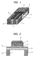
- Fig. 1 schematically illustrates an ink jet head comprising the discharge port 1 through which a liquid, e.g., ink, is discharged, liquid passage 2 by which the individual liquid chamber 3 is in communication with the discharge port 1, common liquid chamber 4, vibrator 5, lower electrode 6, piezoelectric layer 7 and upper electrode 8.
- the piezoelectric layer 7 has a rectangular surface in the vibrator 5 plane direction, as illustrated in Fig. 1 .
- the piezoelectric layer 7 is described in more detail by referring to Fig. 2 , which is a cross-sectional view of the layer shown in Fig. 1 , cut in the width direction, perpendicular to the vibrator 5, where 9: second electrode layer, 7: piezoelectric layer, 5: vibrator, 6: first electrode layer, 8: upper electrode, 12: individual liquid chamber, and 11: partition in the liquid chamber.
- the second electrode layer is patterned like the piezoelectric layer, but may be designed similarly to the first electrode layer 6.
- a preferred embodiment has an anchor layer between the first electrode layer 6 and vibrator 5 (or substrate).
- the preferable materials for the anchor layer include metals, e.g., Ti, Cr, Pb and Ni; and oxides, e.g., TiO 2 .
- the film thickness of the anchor layer is 0.5 to 50 nm, preferably 1 to 20 nm.
- the material constituting the anchor layer may be laminate of the above materials.
- the upper electrode may be multi-layered with a first and second electrodes.
- the layer comprising the layers 7 and 9 has a rectangular cross-section, but may have a trapezoidal or inverted trapezoidal cross-section.
- the order of the layer 8 and electrode layer comprising the layers 6 and 9 may be inverted.
- the structure may comprise, the first electrode layer 6, the second electrode layer 9, and the piezoelectric layer 7 in this order. The inverted structure, caused from a device production process, can secure the same effect.
- the first and second electrode layers 6 and 9 or first electrode layer 6 for the lower electrode extends beyond the piezoelectric layer 7, and the upper electrode extends beyond the element on the side opposite to the lower electrode, to be connected to a driving power source (these situations are not shown).
- the vibrator can be made of a material which has a Young's modulus of 50 GPa or more, preferably 60 GPa or more, and hence can be formed into a plate shape.
- the materials useful for the vibrator 5 include SiO 2 , SiN, SiNO, ZrO 2 (which may be doped with a stabilizing element), Si (which may contain a dopant), stainless steel, Ti, Cr, Ni and Al.
- the vibrator 5 may be 0.5 to 10 ⁇ m thick, preferably 1.0 to 6.0 ⁇ m.
- the electrode layer may be 0.05 to 0.6 ⁇ m thick, preferably 0.08 to 0.3 ⁇ m thick.
- the first layer may be 5 to 450 nm thick, preferably 10 to 200 nm thick
- the second electrode layer may be 5 to 250 nm thick, preferably 10 to 150 nm thick.
- the individual liquid chamber 12 may have a width Wa (see Fig. 5 ) of 30 to 180 ⁇ m, and length Wb (also see Fig. 5 ) of 0.3 to 6.0 mm, although varying depending on quantity of liquid droplets to be discharged.
- the discharge port 1 preferably has a circular or star-shaped cross-section of 7 to 30 ⁇ m in diameter in the plane perpendicular to the opening direction, and a cross-section flaring towards the liquid passage 2 along the opening direction.
- the liquid passage 2 is preferably 0.05 to 0.5 mm long. The liquid droplet discharge speed may be insufficient when a longer passage is used, and fluctuate largely when a shorter one is used.
- the ink jet head of the above structure can be used for ink jet recording units.
- the piezoelectric element of the above structure can give an ink jet head with stable discharge characteristics and long service life, and ink jet recording units with high performance.
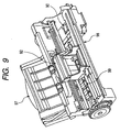
- Fig. 8 outlines an ink jet recording unit which uses the ink jet head of the present invention
- Fig. 9 outlines the ink jet recording unit, with the exteriors 81 to 85 and 87 removed to illustrate the working mechanism.
- the unit comprises the automatic feeder 97 which automatically supplies recording paper as a recording medium into the unit inside, transfer section 99 which sends the recording paper supplied by the automatic feeder 97 to a given recording position and sends the paper from the recording position to the medium discharge port 98, recording member which performs recording on the paper at the recording position, and recovering member 90 which is responsible for recovering treatment for the recording member.
- the ink jet head of the present invention is set in the carriage 92 in the unit.
- Fig. 8 shows a printer as one of the devices to which the ink jet head of the present invention is applicable. However, the ink jet head of the present invention is also applicable to facsimiles, complex machines, copiers and industrial discharging units.
- the dielectric layer is preferably (111)-oriented for production-related considerations, e.g., productivity.
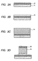
- Figs. 3A to 3D outline a specific process for producing the dielectric element of the present invention.
- the process comprises at least a step for forming the first electrode layer 22 on the substrate 21, step for forming the second electrode layer 23 and step for forming the dielectric layer 24.
- the dielectric element also has the upper electrode layer 26.
- the substrate 21 is made of a material selected from Si, stainless steel and others.
- the substrate material is selected so as to have heat resistance up to 600°C, irrespective of crystallinity and crystal orientation, which is one of the characteristics of the method of the present invention.
- Si(110), Si(100), or stainless steel is preferably selected for the device formation in the latter half process. Selection of an Invor material with low thermal expansion coefficient is a preferred aspect for a stainless steel substrate.
- the Si substrate whether or not it is coated with an oxide layer, can give the element of similar structure, because the present invention is not dependent on crystal structure for the substrate. This brings a production-related merit, because it can dispense with a substrate etching step for removing an oxide layer.
- the electrode and dielectric layer layers can be produced by various methods, e.g., sputtering, MO-CVD, laser-aided abrasion, sol-gel and MBE, of which sputtering, MO-CVD and sol-gel are more preferable, and sputtering and MO-CVD are still more preferable.
- the substrate 21 is coated with the first electrode layer preferably while it is not heated, or heated at a moderate temperature. This prevents a high stress from being generated in the first electrode layer.
- the face-centered cubic metal, described earlier, for the first electrode layer should be selected from those resistant to heat under the heating conditions in the subsequent steps. It is preferably selected from face-centered cubic metals having a half bandwidth of 0.1 to 10°.
- the substrate temperature levels are preferably set to satisfy the relationship T2 ⁇ T3 > T1, where T1: substrate temperature at which the first electrode layer is formed, T2: substrate temperature at which the second electrode layer is formed and T3: substrate temperature at which the dielectric layer is formed. More specifically, T1 is preferably room temperature to 350°C, inclusive, more preferably 100 to 350°C, inclusive; T2 is 300 to 800°C, inclusive; and T3 is preferably 450°C or higher but below 600°C.
- T3 ⁇ T2 the dielectric layer can be formed without any problem, e.g., compositional deviation resulting from release of oxygen from the second electrode layer as the oxide electrode, to give the dielectric element to be assembled in a device while keeping its inherent characteristics.
- the second electrode is preferably produced by forming the above-described perovskite oxide into a film under heating while keeping the substrate at an adequate temperature level.
- the substrate heating temperature is 300 to 800°C, preferably 450 to 620°C.
- the perovskite oxide can be formed into the oxide electrode layer having a half bandwidth of 0.5 to 11° under the above conditions.
- the dielectric element of the present invention can be produced by forming the dielectric layer on the second electrode layer while keeping the substrate on which it is formed while heating the substrate.
- the thin (111)-oriented crystalline film of perovskite structure can be formed as the dielectric film at a lower temperature by forming the dielectric layer on the second electrode layer. The temperature level at which the substrate is to be kept is already described earlier.
- the dielectric layer is preferably formed at around 500°C, and it is recommended that the substrate is kept at 450 to 550°C. Moreover, the dielectric layer can have a half bandwidth of 1.0 to 12° by controlling the operating conditions, e.g., gas pressure.
- the pulsed process in which the starting gas is supplied onto a substrate intermittently rather than continuously is preferable. This is another condition for the process, in addition to substrate temperature.
- the method for producing the dielectric element as the third aspect comprises a step for forming a (100)-oriented YSZ film on a (100)-oriented Si substrate, step for forming a face-centered cubic metal film, step for forming an electrode layer of perovskite oxide, step for forming a (111)-oriented dielectric element, and step for forming another electrode on the dielectric element.
- the YSZ film when formed on a Si substrate heated at around 800°C, can be epitaxially grown while fitting lattice constants of the substrate. It is preferably formed by sputtering. It is particularly preferable to form the film on a substrate coated with a SiO 2 layer having a thickness of 15 nm or less. The SiO 2 layer should be sufficiently thin, having a thickness in the above range, to be depleted by the reaction with metallic Zr deposited thereon.
- the YSZ film is then coated with a (111)-oriented, face-centered cubic metal film.
- a single-crystal electrode layer of perovskite oxide can be also (111)-oriented, when formed on the metal film.
- the (111)-oriented dielectric layer is formed by the method described earlier.
- the method for producing the dielectric layer is applicable to production of ink jet head in which the dielectric element is used as a piezoelectric element.
- the method for producing an ink jet head may fall into the following two general categories.
- the first method at least comprises a step for forming a first electrode layer on a substrate while it is not heated or heated, step for forming, under heating, a second electrode layer which is oriented, electroconductive and mainly composed of a metal oxide, step for forming a (111)-oriented dielectric layer, step for forming an upper electrode layer, step for forming individual liquid chambers and step for forming liquid discharge ports.
- the second method at least comprises a step for forming a first electrode layer on a substrate while it is not heated, step for forming, under heating, a second electrode layer which is oriented, electroconductive and mainly composed of a metal oxide, step for forming a (111)-oriented dielectric layer, step for joining the (111)-oriented dielectric layer to an electrode layer formed on a second substrate, step for removing the first substrate, step for forming individual liquid chambers and step for forming liquid discharge ports.
- the (111)-oriented dielectric layer may be joined to the second substrate after it is provided with a vibrator.
- the first method is the same as the method for producing the dielectric element until the piezoelectric layer is formed, and additionally comprises a step for removing part of the substrate 21 and step for forming the ink discharge ports.
- the substrate is partly removed to form the individual liquid chambers 3 in Fig. 1 or 12 in Fig. 2 .
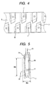
- a plurality of chambers can be formed by treating the substrate by wet etching, dry etching, sand milling or the like, at certain pitches on the substrate. Arranging these chambers 12 in zigzags is a preferred embodiment, as shown in Fig. 4 , which is a plan view of an ink jet head. Referring to Fig.
- the region 12 defined by broken lines represents that for the individual liquid chamber to which a pressure is applied, and the region 7 represents that for the patterned piezoelectric element.
- the piezoelectric layer in the piezoelectric element is composed at least of the dielectric element of the present invention and upper electrode.
- the region 5 represents portion for the vibrator and lower electrode.
- the lower electrode may be patterned, as shown in Figs. 3A to 3D .
- At least the electrode immediately below the dielectric layer has a layered structure with the first and second electrode layers.
- the region for the individual liquid chamber is formed of a parallelogram.
- Fig. 5 is a plan view showing the whole individual liquid chamber, where the upper electrode 26 is connected to a driving circuit by the region 13 extending from the individual liquid chamber 12, and the region 14 represents a restriction in the passage extending from the common liquid chamber to the individual liquid chamber.
- the piezoelectric layer extends into this region, which, however, is not prerequisite.
- the ink discharge port 1 is formed in such a way to connect the substrate on which it is formed, or the discharge port 1 and liquid passage 2 are formed, to another. It can be formed by etching, machining or laser beams.
- the substrate on which the liquid discharge port is formed may be the same as, or different from, the substrate on which the piezoelectric layer is formed.
- the former substrate is made of a material, e.g., stainless steel or Ni, selected from those having a thermal expansion coefficient different by 1E-6 to 1E-8°C from that of a material for the latter substrate.
- the substrates may be joined to each other by an organic adhesive agent, but more preferably by a metal, because it can join them at low 300°C or lower, decreases a differential thermal expansion coefficient with the substrate to avoid problems, e.g., substrate deformation, when length of the dielectric element exceeds a certain level, and decreases damages on the piezoelectric layer.
- the metals useful for joining the substrates include In, Au, Cu, Ni, Pb, Ti, Cr and Pd.
- the second method transfers the piezoelectric layer (dielectric layer) formed on the first substrate to the second substrate. It is the same as the method for producing the dielectric element, illustrated in Figs. 3A to 3D , until the piezoelectric layer is formed. It additionally comprises a step for forming the vibrator 5 on the upper electrode while the piezoelectric layer is kept unpatterned and step for transferring the vibrator to the second electrode, or a step for forming the electrode and/or vibrator on the piezoelectric layer and step for joining the vibrator to the second substrate to transfer the vibrator to the second substrate together with the piezoelectric layer.
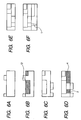
- the second substrate is provided with the individual liquid chamber 12, liquid passage 2 and common liquid chamber 4 by, e.g., the steps shown in Figs. 6A to 6E (the figure shows the steps of 6A to 6F).
- the step shown in Fig. 6A forms a mask on the substrate for each of the individual liquid chambers.
- the step shown in Fig. 6B treats the substrate from the top by etching or the like (the cross-hatched region represents the area to be treated).
- the step shown in Fig. 6C removes the mask and forms a mask for the liquid passage 2.
- the step shown in Fig. 6D forms the liquid passage and common liquid chamber by treating the cross-hatched region on the substrate by etching or the like.
- FIG. 6E schematically illustrates the substrate provided with the individual liquid chamber, liquid passage and common liquid chamber after the mask is removed.
- Fig. 6F shows the substrate joined to the other substrate with the discharge port and part of the common liquid chamber.
- the substrate surface 16 with the liquid discharge port is preferably treated for liquid repellency.
- the second substrate to be joined to the piezoelectric layer on the first substrate is used in the condition illustrated in Fig. 6E or 6F .
- the second substrate having the vibrator on the individual liquid chamber 12 is used ( Fig. 6E or 6F ).
- Fig. 7 illustrates the patterned piezoelectric layer, after the first substrate is joined and then removed.
- the upper electrode 8 shown in Fig. 7 is composed of the second and first electrodes in this order from the vibrator 5 side.
- the piezoelectric may be patterned beforehand or not.
- the metal joint layer it is preferable to use the metal joint layer as the lower electrode.
- the method of the present invention for producing an ink jet head involves patterning of the piezoelectric layer and/or removal of the first substrate in the production process, which is one of the characteristics of the present invention.
- the first electrode layer of a metal can be used as an etching stop layer, which is a preferred embodiment viewed from the process side. Keeping a half bandwidth in the above range minimizes stress changes by the piezoelectric patterning step or substrate removal step, to bring advantages of reducing problems, e.g., cracking, exfoliation or deformation.
- the present invention can produce the dielectric element on a substrate of large area, reduce the device unit cost and improve production through-put.
- the similar effects can be realized in the piezoelectric patterning step, to bring a significant advantage of reducing element characteristic changes, which may be caused by production steps.
- the laminate thus produced had an XRD-determined degree of crystal orientation of 99% or more in the (111) direction running in parallel to the substrate surface.
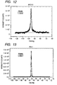
- Half-value bandwidths f3, f2 and f1 of the respective dielectric, second electrode and first electrode layers in the laminate were 3.9, 1.7 and 0.46°, determined by fitting a pseudo-Voigt function, as shown in Figs. 11 to 13 .
- the dielectric and second electrode layers were analyzed using the (101) peak, as described earlier.
- the laminate was then coated with a 100 nm thick SRO layer as an upper electrode, to produce the dielectric element of the present invention. It had a remanent polarization 2Pr of 47 ⁇ C/cm 2 and coercive force Ec of 71 kV/cm, determined by the electrical analysis. These properties are sufficient to make the element useful for ferroelectric memories.
- a 200 ⁇ m thick (110)-oriented Si substrate was coated with a 1.5 ⁇ m thick SiN layer by sputtering; 5 nm thick Ti layer as an anchor layer and 50 nm thick Ir electrode layer by rf sputtering while controlling the substrate at 200°C; 100 nm thick SRO layer as a second electrode layer also by rf sputtering while controlling the substrate at 600°C; 2.5 ⁇ m thick piezoelectric layer of Pb(Zr, Ti)O 3 (Zr/Ti ratio: 48/52); and a Pt/Cr layer as an upper electrode, where the piezoelectric layer was patterned with 45 ⁇ m wide, 3 mm long rectangles.
- Fig. 2 is a cross-sectional view of the piezoelectric element for one patterning.
- the first electrode layer sufficiently worked as an etching stop layer in the production process.
- the piezoelectric element exhibited a good displacement of 0.15 m, when a voltage of 20 V was applied thereto.
- All of the PZT, SRO and Ir layers which constituted the piezoelectric element had a degree of crystal orientation of 99% or more in the (111) direction, and half bandwidths f1, f2 and f3 of 0.53, 2.1 and 4.5°, determined in the same manner as in EXAMPLE 1.
- the stainless steel substrate provided with the liquid passage 2, discharge port 1 and ink supply passage ( Fig. 10 ) was joined in the above element, to produce the ink jet head of the present invention.
- the element was confirmed to discharge liquid droplets smoothly at a driving voltage of 20 V. It was also confirmed that characteristic variations were limited port by port and device by device.
- a (110)-oriented Si substrate was coated with a 100 nm thick Pt layer as a first electrode layer (substrate temperature controlled at 250°C), 60 nm thick LaNiO 3 layer as a second electrode layer and 3.0. ⁇ m thick Pb(Zr, Ti)O 3 (Zr/Ti ratio: 50/50) layer as a piezoelectric layer while controlling the substrate at T1 of room temperature, T2 of 650°C and T3 of 520°C.
- the piezoelectric layer was coated with a 200 nm thick Pt/Ti electrode layer and 2.0 ⁇ m thick SiN layer as a vibrator.
- the substrate was joined to a second Si substrate, prepared to have a condition illustrated in Fig.
- the (100)-oriented Si substrate was removed by etching with an alkali.
- the first and second electrode layers were patterned by ICP.
- the piezoelectric layer was patterned by etching with a mixed acid as an etchant, to be left on the individual liquid chambers.
- the resulting laminate was joined to a stainless steel (SUS) plate provided with discharge ports of 20 ⁇ m in diameter, to produce the ink jet head of the present invention. The discharge characteristics were evaluated, and the results similar to those observed in EXAMPLE 2 were produced.
- the first electrode layer, second electrode layer and piezoelectric layer had a degree of crystal orientation of 99% in the (111) direction, and half bandwidths f1, f2 and f3 of 0.56, 2.0 and 3.3°.
- the ink jet head with the first electrode layer replaced by a (110)-oriented Si substrate exhibited characteristics not different much.
- a Si substrate coated with a 20 nm thick SiO 2 layer was coated with a TiO 2 layer, and then with a 70 nm thick (111)-oriented Pt layer while controlling the substrate at 200°C.
- the resulting laminate was then coated with a 300 nm thick (111)-oriented PZT (Zr/Ti ratio: 40/60) layer either directly or via a 40 nm thick (111)-oriented SRO layer by a pulsed MO-CVD process while controlling the substrate at 500°C, to evaluate the ferroelectric characteristics.
- the SRO film was provided while controlling the substrate at 600°C.
- the resultant piezoelectric element of the present invention with the SRO layer had a remanent polarization 2Pr of 44 ⁇ C/cm 2 , whereas the SRO-free one had a value of 21 ⁇ C/cm 2 .
- the layers had half bandwidths f1, f2 and f3 of 0.63, 2.9 and 4.4°.
- a substrate of (111)-oriented, single-crystal MgO was coated with a 100 nm thick Pt layer by sputtering while controlling the substrate at 600°C to form the (111)-oriented layer thereon. It was then coated with a 15 nm thick SRO layer while controlling the substrate at 650°C and then with a PZT (Zr/Ti ratio: 48/52) layer while controlling the substrate at 600°C by sputtering for both layers. These layers had half bandwidths f1, f2 and f3 of 0.09, 0.48 and 1.5°. The half bandwidth of the PZT layer was fairly wide.
- the laminate showed exfoliation in places, when joined to a second substrate in the same manner as in EXAMPLE 3, and needed some improvement. It was also observed that crystallinity of the PZT layer varied widely, when it was directly in contact with the Pt layer, i.e., without a PbTiO 3 layer in-between.
- a (100)-oriented Si substrate was rinsed (treated) to remove a surface oxide layer, and then with H 2 O 2 to form an oxide layer thereon. It was coated with a Zr layer by sputtering with a metal target while controlling the substrate at 800°C, and then with a YSZ layer with a target containing the Y component at 30%.
- the YSZ layer was a (100)-oriented, single-crystal, epitaxial layer.
- the substrate coated with these layers to a total thickness of 30 to 60 nm was coated with a 50 to 80 nm Pt layer while controlling the substrate at 60°C.
- the Pt layer had a half bandwidth f1 of 0.10°.
- Both Pt and SRO layers were (111)-oriented and single-crystalline.
- a PZT layer was then formed on the above laminate. It was found that the (111)-oriented and single-crystalline could be formed.
- a (111)-oriented, SRO-free Pt layer was coated with a PZT layer.
- the PZT layer was not single-crystalline, randomly oriented in the in-plane direction and containing a (110) component in the out-of-plane direction.
Landscapes
- Engineering & Computer Science (AREA)
- Manufacturing & Machinery (AREA)
- Chemical & Material Sciences (AREA)
- Ceramic Engineering (AREA)
- Particle Formation And Scattering Control In Inkjet Printers (AREA)
Claims (13)
- Dielektrisches Element, umfassend eine untere Elektrodenschicht (6, 9), eine dielektrische Perowskit-Schicht (7) und eine obere Elektrodenschicht (8) in dieser Reihenfolge auf einem Substrat, dadurch gekennzeichnet, dass mindestens eine der unteren und der oberen Elektrodenschicht eine erste, hauptsächlich aus Metall bestehende Elektrodenschicht (6) und eine zweite, hauptsächlich aus einem Perowskit-Oxid bestehende Elektrodenschicht (9) umfasst, wobei die zweite Elektrodenschicht auf einer Seite der dielektrischen Schicht gebildet ist,
jede der ersten Elektrodenschicht (6), der zweiten Elektrodenschicht (9) und der dielektrischen Schicht (7) eine bevorzugte (111)- oder uniaxial orientierte (111)-Kristallstruktur aufweist, und
die erste Elektrodenschicht, die zweite Elektrodenschicht und die dielektrische Schicht die Beziehung gemäß folgender allgemeiner Formel (1) erfüllen:
- Dielektrisches Element nach Anspruch 1,
bei dem das Metall in der ersten Elektrodenschicht ein kubischflächenzentrierter Kristall ist. - Dielektrisches Element nach Anspruch 1 oder 2,
bei dem die zweite Elektrodenschicht eine Halbbandbreite f2 des XRD-Peaks in einem Bereich von 0,5 bis 3,0°, bestimmt durch Anpassen einer Pseudo-Voigt-Funktion, in der (101)-Richtung, die nicht rechtwinklig zu der Oberfläche der zweiten Elektrodenschicht ist, aufweist. - Dielektrisches Element nach einem der Ansprüche 1 bis 3,
bei dem die dielektrische Schicht eine Halbbandbreite f3 des XRD-Peaks im Bereich von 1,0 bis 6,0°, bestimmt durch Anpassen einer Pseudo-Voigt-Funktion in der (101)-Richtung, die nicht rechtwinklig zu der Oberfläche der dielektrischen Schicht ist, aufweist. - Dielektrisches Element nach Anspruch 4,
bei dem das Substrat aus Silicium hergestellt ist und eine SiO2-Schicht einer Dicke von 5 nm oder mehr als Zwischenschicht auf dem Substrat gebildet ist. - Dielektrisches Element nach einem der Ansprüche 1 bis 5,
bei dem die dielektrische Schicht einen Kristallorientierungsgrad von 80 % oder mehr in der (111)-Richtung aufweist. - Dielektrisches Element nach Anspruch 6,
bei dem die dielektrische Schicht einen Kristallorientierungsgrad von 99 % oder mehr in der (111)-Richtung aufweist. - Dielektrisches Element, umfassend eine untere Elektrodenschicht (6, 9), eine dielektrische Schicht (7) und eine obere Elektrodenschicht (8) in dieser Reihenfolge auf einem Substrat,
dadurch gekennzeichnet, dass
mindestens eine der unteren und der oberen Elektrodenschicht eine erste, hauptsächlich aus Metall bestehende Elektrodenschicht (6) und eine zweite, hauptsächlich aus einem Perowskit-Oxid bestehende Elektrodenschicht (9) umfasst, wobei die zweite Elektrodenschicht auf einer Seite der dielektrischen Schicht gebildet ist,
die erste Elektrodenschicht, die zweite Elektrodenschicht und die dielektrische Schicht je eine Einkristallschicht sind, wobei die dielektrische Schicht eine in (1 1 1)-Richtung orientierte Perowskit-Struktur aufweist, und
die erste Elektrodenschicht, die zweite Elektrodenschicht und die dielektrische Schicht die durch die allgemeine Formel (1) repräsentierte Beziehung erfüllen: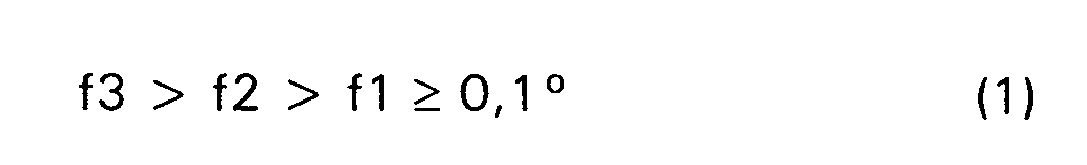
- Dielektrisches Element nach Anspruch 8, weiterhin umfassend
eine (100)-orientierte einkristalline Schicht, die 1 bis 20 Gew.-% Y2O3 inklusive und den Rest ZrO2 enthält; und außerdem umfassend:eine (111)-orientierte einkristalline Schicht aus einem kubisch-flächenzentrierten Metall als die erste Schicht (6);eine (111)-orientierte einkristalline Schicht aus Perowskit-Oxid als zweite Schicht (9); undeine (111)-orientierte einkristalline Schicht aus Perowskit-Oxid als die dielektrische Schicht (7),die in der genannten Reihenfolge auf einem (100)-orientierten Siliciumsubstrat gebildet sind. - Dielektrisches Element nach Anspruch 1 oder 8,
bei dem die erste Elektrodenschicht (6) vornehmlich aus einem Metall in Form eines kubisch-flächenzentrierten Metalls zusammengesetzt ist,
die zweite Elektrodenschicht (9) benachbart zu der ersten Elektrodenschicht angeordnet ist und eine Halbbandbreite des XRD-(101)-Peaks in einem Bereich von 0,5 bis 11 ° aufweist, bestimmt durch Anpassen einer Pseudo-Voigt-Funktion, und
die dielektrische Schicht (7) eine Halbbandbreite des XRD-(101)-Peaks in einem Bereich von 1,0 bis 12° aufweist, bestimmt durch Anpassen einer Pseudo-Voigt-Funktion. - Piezoelektrisches Element mit dem dielektrischen Element nach einem der Ansprüche 1 und 8 bis 10.
- Tintenstrahlkopf, umfassend
einen Flüssigkeitskanal (2), der strömungsverbunden ist mit einer Ausstoßöffnung (1), aus der eine Flüssigkeit ausgestoßen wird, und ein piezoelektrisches Element, welches Energie der in dem Flüssigkeitskanal befindlichen Flüssigkeit zuführt, um diese aus der Ausstoßöffnung auszustoßen, wobei das piezoelektrische Element ein Element gemäß Anspruch 11 ist. - Verfahren zum Fertigen des dielektrischen Elements nach einem der Ansprüche 1 und 8 bis 12,
bei dem die Substrat-Temperaturwerte so eingestellt werden, dass die Beziehung gemäß nachstehender allgemeiner Formel (2) erfüllt ist:
worin bedeuten
T1: Substrattemperatur, bei der die erste Elektrodenschicht gebildet wird,
T2: Substrattemperatur, bei der die zweite Elektrodenschicht gebildet wird,
T3: Substrattemperatur, bei der die dielektrische Schicht gebildet wird.
Applications Claiming Priority (2)
| Application Number | Priority Date | Filing Date | Title |
|---|---|---|---|
| JP2004004748 | 2004-01-09 | ||
| JP2004004748 | 2004-01-09 |
Publications (3)
| Publication Number | Publication Date |
|---|---|
| EP1560278A1 EP1560278A1 (de) | 2005-08-03 |
| EP1560278B1 true EP1560278B1 (de) | 2008-12-17 |
| EP1560278B9 EP1560278B9 (de) | 2009-08-19 |
Family
ID=34650737
Family Applications (1)
| Application Number | Title | Priority Date | Filing Date |
|---|---|---|---|
| EP05000307A Ceased EP1560278B9 (de) | 2004-01-09 | 2005-01-08 | Dielektrisches Element, piezoelektrisches Element, Tintenstrahlkopf und Verfahren zur Herstellung dieses Kopfes |
Country Status (6)
| Country | Link |
|---|---|
| US (1) | US7262544B2 (de) |
| EP (1) | EP1560278B9 (de) |
| KR (1) | KR100875315B1 (de) |
| CN (1) | CN100457458C (de) |
| DE (1) | DE602005011690D1 (de) |
| TW (1) | TWI264839B (de) |
Families Citing this family (33)
| Publication number | Priority date | Publication date | Assignee | Title |
|---|---|---|---|---|
| KR100672883B1 (ko) * | 2003-01-31 | 2007-01-24 | 캐논 가부시끼가이샤 | 압전 소자 |
| JP4717344B2 (ja) * | 2003-12-10 | 2011-07-06 | キヤノン株式会社 | 誘電体薄膜素子、圧電アクチュエータおよび液体吐出ヘッド |
| TWI255057B (en) * | 2004-02-27 | 2006-05-11 | Canon Kk | Dielectric element, piezoelectric element, ink jet head and ink jet recording apparatus and manufacturing method of same |
| JP2005244133A (ja) * | 2004-02-27 | 2005-09-08 | Canon Inc | 誘電体素子、圧電素子、インクジェットヘッド及びインクジェット記録装置、並びにこれらの製造方法 |
| US7235917B2 (en) * | 2004-08-10 | 2007-06-26 | Canon Kabushiki Kaisha | Piezoelectric member element and liquid discharge head comprising element thereof |
| US8082640B2 (en) * | 2004-08-31 | 2011-12-27 | Canon Kabushiki Kaisha | Method for manufacturing a ferroelectric member element structure |
| JP2006069152A (ja) * | 2004-09-06 | 2006-03-16 | Canon Inc | インクジェットヘッド及びその製造方法 |
| US20070046153A1 (en) * | 2005-08-23 | 2007-03-01 | Canon Kabushiki Kaisha | Piezoelectric substrate, piezoelectric element, liquid discharge head and liquid discharge apparatus |
| US7998362B2 (en) * | 2005-08-23 | 2011-08-16 | Canon Kabushiki Kaisha | Piezoelectric substance, piezoelectric element, liquid discharge head using piezoelectric element, liquid discharge apparatus, and production method of piezoelectric element |
| US7528532B2 (en) * | 2005-08-23 | 2009-05-05 | Canon Kabushiki Kaisha | Piezoelectric substance and manufacturing method thereof, piezoelectric element and liquid discharge head using such piezoelectric element and liquid discharge apparatus |
| US7528530B2 (en) * | 2005-08-23 | 2009-05-05 | Canon Kabushiki Kaisha | Piezoelectric substance, piezoelectric substance element, liquid discharge head, liquid discharge device and method for producing piezoelectric substance |
| US7591543B2 (en) * | 2005-08-23 | 2009-09-22 | Canon Kabushiki Kaisha | Piezoelectric member, piezoelectric member element, liquid discharge head in use thereof, liquid discharge apparatus and method of manufacturing piezoelectric member |
| US7521845B2 (en) * | 2005-08-23 | 2009-04-21 | Canon Kabushiki Kaisha | Piezoelectric substance, piezoelectric element, liquid discharge head using piezoelectric element, and liquid discharge apparatus |
| US8142678B2 (en) * | 2005-08-23 | 2012-03-27 | Canon Kabushiki Kaisha | Perovskite type oxide material, piezoelectric element, liquid discharge head and liquid discharge apparatus using the same, and method of producing perovskite type oxide material |
| US7759845B2 (en) * | 2006-03-10 | 2010-07-20 | Canon Kabushiki Kaisha | Piezoelectric substance element, liquid discharge head utilizing the same and optical element |
| JP5188076B2 (ja) * | 2006-04-03 | 2013-04-24 | キヤノン株式会社 | 圧電素子及びその製造方法、電子デバイス、インクジェット装置 |
| CN101641806B (zh) * | 2007-03-30 | 2011-11-30 | 佳能株式会社 | 外延膜、压电元件、铁电元件、它们的制造方法以及液体排出头 |
| JP2008258516A (ja) * | 2007-04-09 | 2008-10-23 | Funai Electric Co Ltd | 圧電素子及び結晶質セラミックスの成膜方法 |
| JP4361102B2 (ja) * | 2007-09-12 | 2009-11-11 | 富士フイルム株式会社 | 圧電素子の製造方法 |
| JP5531653B2 (ja) * | 2010-02-02 | 2014-06-25 | 日立金属株式会社 | 圧電薄膜素子、その製造方法及び圧電薄膜デバイス |
| JP5440697B2 (ja) * | 2010-05-17 | 2014-03-12 | 株式会社村田製作所 | 圧電アクチュエータ及び駆動装置 |
| US8456061B2 (en) * | 2011-01-25 | 2013-06-04 | Hewlett-Packard Development Company, L.P. | Architecture for piezoelectric MEMS devices |
| US8426270B2 (en) * | 2011-07-22 | 2013-04-23 | Intermolecular, Inc. | Memory device with a textured lowered electrode |
| US8866367B2 (en) | 2011-10-17 | 2014-10-21 | The United States Of America As Represented By The Secretary Of The Army | Thermally oxidized seed layers for the production of {001} textured electrodes and PZT devices and method of making |
| US9761785B2 (en) | 2011-10-17 | 2017-09-12 | The United States Of America As Represented By The Secretary Of The Army | Stylo-epitaxial piezoelectric and ferroelectric devices and method of manufacturing |
| JP2013197522A (ja) * | 2012-03-22 | 2013-09-30 | Ricoh Co Ltd | 圧電体薄膜素子とその製造方法、該圧電体薄膜素子を用いた液滴吐出ヘッドおよびインクジェット記録装置 |
| JP2017063138A (ja) * | 2015-09-25 | 2017-03-30 | 株式会社リコー | 圧電体膜、圧電デバイス、圧電体膜の製造方法 |
| JP2017092097A (ja) * | 2015-11-04 | 2017-05-25 | セイコーエプソン株式会社 | 圧電素子、超音波プローブ、超音波測定装置及び圧電素子の製造方法 |
| JP6733941B1 (ja) * | 2019-03-22 | 2020-08-05 | 大口マテリアル株式会社 | 半導体素子搭載用基板 |
| JP7034384B2 (ja) * | 2019-12-18 | 2022-03-11 | 日本碍子株式会社 | 振動板と支持基板との接合体およびその製造方法 |
| JP7667052B2 (ja) * | 2021-09-27 | 2025-04-22 | 富士フイルム株式会社 | 圧電積層体及び圧電素子 |
| EP4216245A3 (de) | 2022-01-19 | 2023-11-22 | Samsung Electronics Co., Ltd. | Kondensator, halbleiterbauelement mit dem kondensator und verfahren zur herstellung des kondensators |
| CN116046029B (zh) * | 2023-03-27 | 2023-07-14 | 成都凯天电子股份有限公司 | 压电式力学传感器温度漂移补偿结构及其补偿方法 |
Citations (1)
| Publication number | Priority date | Publication date | Assignee | Title |
|---|---|---|---|---|
| JP2003179278A (ja) * | 2001-12-10 | 2003-06-27 | Seiko Epson Corp | 圧電アクチュエータ及びインクジェット式記録ヘッド |
Family Cites Families (15)
| Publication number | Priority date | Publication date | Assignee | Title |
|---|---|---|---|---|
| JP3104550B2 (ja) | 1994-10-17 | 2000-10-30 | 松下電器産業株式会社 | 圧電アクチュエータおよびその製造方法 |
| JP3209082B2 (ja) | 1996-03-06 | 2001-09-17 | セイコーエプソン株式会社 | 圧電体薄膜素子及びその製造方法、並びにこれを用いたインクジェット式記録ヘッド |
| JP3796394B2 (ja) | 2000-06-21 | 2006-07-12 | キヤノン株式会社 | 圧電素子の製造方法および液体噴射記録ヘッドの製造方法 |
| JP3833070B2 (ja) * | 2001-02-09 | 2006-10-11 | キヤノン株式会社 | 液体噴射ヘッドおよび製造方法 |
| JP3754897B2 (ja) * | 2001-02-09 | 2006-03-15 | キヤノン株式会社 | 半導体装置用基板およびsoi基板の製造方法 |
| KR100865652B1 (ko) * | 2001-05-11 | 2008-10-29 | 우베 고산 가부시키가이샤 | 압전 박막 공진자 |
| US6663989B2 (en) * | 2001-06-06 | 2003-12-16 | Max-Planck-Institut Fur Mikrostrukturphysik | Non c-axis oriented bismuth-layered perovskite ferroelectric structure epitaxially grown on buffered silicon |
| JP3817730B2 (ja) * | 2001-12-10 | 2006-09-06 | セイコーエプソン株式会社 | 圧電アクチュエータの製造方法、インクジェット式記録ヘッド、及びプリンタ |
| JP2004006722A (ja) * | 2002-03-27 | 2004-01-08 | Seiko Epson Corp | 圧電アクチュエータ、インクジェット式ヘッド及び吐出装置 |
| JP4086535B2 (ja) * | 2002-04-18 | 2008-05-14 | キヤノン株式会社 | アクチュエータ及びインクジェットヘッドの製造方法 |
| US6969157B2 (en) * | 2002-05-31 | 2005-11-29 | Matsushita Electric Industrial Co., Ltd. | Piezoelectric element, ink jet head, angular velocity sensor, method for manufacturing the same, and ink jet recording apparatus |
| JP4708667B2 (ja) * | 2002-08-08 | 2011-06-22 | キヤノン株式会社 | アクチュエータおよび液体噴射ヘッド |
| JP4457587B2 (ja) * | 2002-09-05 | 2010-04-28 | セイコーエプソン株式会社 | 電子デバイス用基体の製造方法及び電子デバイスの製造方法 |
| JP3873935B2 (ja) * | 2003-06-18 | 2007-01-31 | セイコーエプソン株式会社 | 強誘電体メモリ素子 |
| JP4165347B2 (ja) * | 2003-06-25 | 2008-10-15 | セイコーエプソン株式会社 | 圧電素子の製造方法 |
-
2004
- 2004-12-30 US US11/024,961 patent/US7262544B2/en not_active Expired - Lifetime
-
2005
- 2005-01-03 TW TW094100090A patent/TWI264839B/zh not_active IP Right Cessation
- 2005-01-07 CN CNB200510004145XA patent/CN100457458C/zh not_active Expired - Fee Related
- 2005-01-07 KR KR1020050001473A patent/KR100875315B1/ko not_active Expired - Fee Related
- 2005-01-08 EP EP05000307A patent/EP1560278B9/de not_active Ceased
- 2005-01-08 DE DE602005011690T patent/DE602005011690D1/de not_active Expired - Lifetime
Patent Citations (1)
| Publication number | Priority date | Publication date | Assignee | Title |
|---|---|---|---|---|
| JP2003179278A (ja) * | 2001-12-10 | 2003-06-27 | Seiko Epson Corp | 圧電アクチュエータ及びインクジェット式記録ヘッド |
Also Published As
| Publication number | Publication date |
|---|---|
| US20050168112A1 (en) | 2005-08-04 |
| CN1636729A (zh) | 2005-07-13 |
| TW200529480A (en) | 2005-09-01 |
| KR100875315B1 (ko) | 2008-12-19 |
| EP1560278A1 (de) | 2005-08-03 |
| TWI264839B (en) | 2006-10-21 |
| EP1560278B9 (de) | 2009-08-19 |
| KR20050073410A (ko) | 2005-07-13 |
| DE602005011690D1 (de) | 2009-01-29 |
| CN100457458C (zh) | 2009-02-04 |
| US7262544B2 (en) | 2007-08-28 |
Similar Documents
| Publication | Publication Date | Title |
|---|---|---|
| EP1560278B9 (de) | Dielektrisches Element, piezoelektrisches Element, Tintenstrahlkopf und Verfahren zur Herstellung dieses Kopfes | |
| EP1585180B1 (de) | Dielektrisches Element, piezoelektrisches Element, Tintenstrahlkopf, Tintenstrahlaufzeichnungsgerät sowie deren Herstellungsverfahren | |
| KR100581257B1 (ko) | 압전소자, 잉크젯헤드, 각속도센서 및 이들의 제조방법,그리고 잉크젯방식 기록장치 | |
| JP4717344B2 (ja) | 誘電体薄膜素子、圧電アクチュエータおよび液体吐出ヘッド | |
| US7517063B2 (en) | Piezoelectric element | |
| KR100738290B1 (ko) | 유전체 소자, 압전체 소자, 잉크 제트 헤드 및 잉크 제트기록 장치, 및 그 제조 방법 | |
| JP5164052B2 (ja) | 圧電体素子、液体吐出ヘッド及び液体吐出装置 | |
| KR100748727B1 (ko) | 유전체 소자, 압전 소자, 잉크젯 헤드 및 잉크젯 기록 장치, 및 그 제조 방법 | |
| JP2005175099A5 (de) | ||
| US7528530B2 (en) | Piezoelectric substance, piezoelectric substance element, liquid discharge head, liquid discharge device and method for producing piezoelectric substance | |
| JP2004071933A (ja) | アクチュエータおよび液体噴射ヘッドならびに前記液体噴射ヘッドの製造方法 | |
| JP2004186646A (ja) | 圧電素子、インクジェットヘッド及びこれらの製造方法、並びにインクジェット式記録装置 | |
| JP4250593B2 (ja) | 誘電体素子、圧電体素子、インクジェットヘッド及びその製造方法 | |
| JP2005119166A (ja) | 圧電素子、インクジェットヘッド、及びこれらの製造方法、並びにインクジェット式記録装置 | |
| JP2003188431A (ja) | 圧電素子、インクジェットヘッドおよびそれらの製造方法、並びにインクジェット式記録装置 | |
| JP4689482B2 (ja) | 圧電アクチュエーター、圧電アクチュエーターの製造方法、液体吐出ヘッド |
Legal Events
| Date | Code | Title | Description |
|---|---|---|---|
| PUAI | Public reference made under article 153(3) epc to a published international application that has entered the european phase |
Free format text: ORIGINAL CODE: 0009012 |
|
| AK | Designated contracting states |
Kind code of ref document: A1 Designated state(s): AT BE BG CH CY CZ DE DK EE ES FI FR GB GR HU IE IS IT LI LT LU MC NL PL PT RO SE SI SK TR |
|
| AX | Request for extension of the european patent |
Extension state: AL BA HR LV MK YU |
|
| 17P | Request for examination filed |
Effective date: 20051216 |
|
| AKX | Designation fees paid |
Designated state(s): DE FR GB IT |
|
| 17Q | First examination report despatched |
Effective date: 20060112 |
|
| GRAP | Despatch of communication of intention to grant a patent |
Free format text: ORIGINAL CODE: EPIDOSNIGR1 |
|
| RIN1 | Information on inventor provided before grant (corrected) |
Inventor name: ASANO, GOJI Inventor name: OKAMOTO, SHOJI Inventor name: FUNAKUBO, HIROSHI Inventor name: FUKUI, TETSURO Inventor name: TAKEDA, KENICHI Inventor name: AOKI, KATSUMI |
|
| GRAS | Grant fee paid |
Free format text: ORIGINAL CODE: EPIDOSNIGR3 |
|
| GRAA | (expected) grant |
Free format text: ORIGINAL CODE: 0009210 |
|
| AK | Designated contracting states |
Kind code of ref document: B1 Designated state(s): DE FR GB IT |
|
| REG | Reference to a national code |
Ref country code: GB Ref legal event code: FG4D |
|
| REF | Corresponds to: |
Ref document number: 602005011690 Country of ref document: DE Date of ref document: 20090129 Kind code of ref document: P |
|
| PLBE | No opposition filed within time limit |
Free format text: ORIGINAL CODE: 0009261 |
|
| STAA | Information on the status of an ep patent application or granted ep patent |
Free format text: STATUS: NO OPPOSITION FILED WITHIN TIME LIMIT |
|
| 26N | No opposition filed |
Effective date: 20090918 |
|
| REG | Reference to a national code |
Ref country code: FR Ref legal event code: PLFP Year of fee payment: 12 |
|
| REG | Reference to a national code |
Ref country code: FR Ref legal event code: PLFP Year of fee payment: 13 |
|
| REG | Reference to a national code |
Ref country code: FR Ref legal event code: PLFP Year of fee payment: 14 |
|
| PGFP | Annual fee paid to national office [announced via postgrant information from national office to epo] |
Ref country code: FR Payment date: 20191216 Year of fee payment: 16 |
|
| PGFP | Annual fee paid to national office [announced via postgrant information from national office to epo] |
Ref country code: GB Payment date: 20200102 Year of fee payment: 16 Ref country code: DE Payment date: 20191224 Year of fee payment: 16 Ref country code: IT Payment date: 20200114 Year of fee payment: 16 |
|
| REG | Reference to a national code |
Ref country code: DE Ref legal event code: R119 Ref document number: 602005011690 Country of ref document: DE |
|
| GBPC | Gb: european patent ceased through non-payment of renewal fee |
Effective date: 20210108 |
|
| PG25 | Lapsed in a contracting state [announced via postgrant information from national office to epo] |
Ref country code: FR Free format text: LAPSE BECAUSE OF NON-PAYMENT OF DUE FEES Effective date: 20210131 |
|
| PG25 | Lapsed in a contracting state [announced via postgrant information from national office to epo] |
Ref country code: DE Free format text: LAPSE BECAUSE OF NON-PAYMENT OF DUE FEES Effective date: 20210803 Ref country code: GB Free format text: LAPSE BECAUSE OF NON-PAYMENT OF DUE FEES Effective date: 20210108 |
|
| PG25 | Lapsed in a contracting state [announced via postgrant information from national office to epo] |
Ref country code: IT Free format text: LAPSE BECAUSE OF NON-PAYMENT OF DUE FEES Effective date: 20210108 |