EP1557880A1 - Harzzusammensetzung um Halbleiter zu verkapseln - Google Patents
Harzzusammensetzung um Halbleiter zu verkapseln Download PDFInfo
- Publication number
- EP1557880A1 EP1557880A1 EP20050000896 EP05000896A EP1557880A1 EP 1557880 A1 EP1557880 A1 EP 1557880A1 EP 20050000896 EP20050000896 EP 20050000896 EP 05000896 A EP05000896 A EP 05000896A EP 1557880 A1 EP1557880 A1 EP 1557880A1
- Authority
- EP
- European Patent Office
- Prior art keywords
- resin composition
- resin
- semiconductor
- sheet
- epoxy
- Prior art date
- Legal status (The legal status is an assumption and is not a legal conclusion. Google has not performed a legal analysis and makes no representation as to the accuracy of the status listed.)
- Withdrawn
Links
- 239000011342 resin composition Substances 0.000 title claims abstract description 174
- 239000004065 semiconductor Substances 0.000 title claims abstract description 157
- 239000003822 epoxy resin Substances 0.000 claims abstract description 51
- 229920000647 polyepoxide Polymers 0.000 claims abstract description 51
- 239000003795 chemical substances by application Substances 0.000 claims abstract description 44
- 239000002245 particle Substances 0.000 claims abstract description 44
- VYPSYNLAJGMNEJ-UHFFFAOYSA-N Silicium dioxide Chemical compound O=[Si]=O VYPSYNLAJGMNEJ-UHFFFAOYSA-N 0.000 claims abstract description 43
- 125000003700 epoxy group Chemical group 0.000 claims abstract description 9
- 238000002834 transmittance Methods 0.000 claims description 22
- 238000001723 curing Methods 0.000 description 64
- 238000000034 method Methods 0.000 description 42
- 229920005989 resin Polymers 0.000 description 37
- 239000011347 resin Substances 0.000 description 37
- ZWEHNKRNPOVVGH-UHFFFAOYSA-N 2-Butanone Chemical compound CCC(C)=O ZWEHNKRNPOVVGH-UHFFFAOYSA-N 0.000 description 36
- 239000000203 mixture Substances 0.000 description 27
- 238000005476 soldering Methods 0.000 description 27
- 238000004519 manufacturing process Methods 0.000 description 23
- 230000000052 comparative effect Effects 0.000 description 22
- 229910000679 solder Inorganic materials 0.000 description 14
- 239000004593 Epoxy Substances 0.000 description 13
- 238000005538 encapsulation Methods 0.000 description 13
- 239000000463 material Substances 0.000 description 13
- 238000002844 melting Methods 0.000 description 13
- 239000011256 inorganic filler Substances 0.000 description 12
- 229910003475 inorganic filler Inorganic materials 0.000 description 12
- 239000000047 product Substances 0.000 description 11
- 238000012360 testing method Methods 0.000 description 11
- 238000000227 grinding Methods 0.000 description 10
- 229920001187 thermosetting polymer Polymers 0.000 description 10
- XEKOWRVHYACXOJ-UHFFFAOYSA-N Ethyl acetate Chemical compound CCOC(C)=O XEKOWRVHYACXOJ-UHFFFAOYSA-N 0.000 description 9
- YXFVVABEGXRONW-UHFFFAOYSA-N Toluene Chemical compound CC1=CC=CC=C1 YXFVVABEGXRONW-UHFFFAOYSA-N 0.000 description 9
- 238000005520 cutting process Methods 0.000 description 9
- 230000008018 melting Effects 0.000 description 9
- 229920005992 thermoplastic resin Polymers 0.000 description 9
- ISWSIDIOOBJBQZ-UHFFFAOYSA-N phenol group Chemical group C1(=CC=CC=C1)O ISWSIDIOOBJBQZ-UHFFFAOYSA-N 0.000 description 8
- 239000000377 silicon dioxide Substances 0.000 description 8
- 238000010438 heat treatment Methods 0.000 description 6
- 239000007788 liquid Substances 0.000 description 6
- 239000003960 organic solvent Substances 0.000 description 6
- 239000000758 substrate Substances 0.000 description 6
- RIOQSEWOXXDEQQ-UHFFFAOYSA-N triphenylphosphine Chemical compound C1=CC=CC=C1P(C=1C=CC=CC=1)C1=CC=CC=C1 RIOQSEWOXXDEQQ-UHFFFAOYSA-N 0.000 description 6
- CSCPPACGZOOCGX-UHFFFAOYSA-N Acetone Chemical compound CC(C)=O CSCPPACGZOOCGX-UHFFFAOYSA-N 0.000 description 5
- XUIMIQQOPSSXEZ-UHFFFAOYSA-N Silicon Chemical compound [Si] XUIMIQQOPSSXEZ-UHFFFAOYSA-N 0.000 description 5
- LNEPOXFFQSENCJ-UHFFFAOYSA-N haloperidol Chemical compound C1CC(O)(C=2C=CC(Cl)=CC=2)CCN1CCCC(=O)C1=CC=C(F)C=C1 LNEPOXFFQSENCJ-UHFFFAOYSA-N 0.000 description 5
- 229920006267 polyester film Polymers 0.000 description 5
- 229910052710 silicon Inorganic materials 0.000 description 5
- 239000010703 silicon Substances 0.000 description 5
- 239000000243 solution Substances 0.000 description 5
- 239000002904 solvent Substances 0.000 description 5
- -1 benzoxazine cyclic compounds Chemical class 0.000 description 4
- 239000004841 bisphenol A epoxy resin Substances 0.000 description 4
- 239000004842 bisphenol F epoxy resin Substances 0.000 description 4
- 229920001577 copolymer Polymers 0.000 description 4
- 238000009826 distribution Methods 0.000 description 4
- 238000001035 drying Methods 0.000 description 4
- 150000002148 esters Chemical class 0.000 description 4
- 239000011521 glass Substances 0.000 description 4
- 125000002887 hydroxy group Chemical group [H]O* 0.000 description 4
- 239000011259 mixed solution Substances 0.000 description 4
- 229920003986 novolac Polymers 0.000 description 4
- 239000005011 phenolic resin Substances 0.000 description 4
- 230000008569 process Effects 0.000 description 4
- 239000002994 raw material Substances 0.000 description 4
- 230000035882 stress Effects 0.000 description 4
- XLYOFNOQVPJJNP-UHFFFAOYSA-N water Substances O XLYOFNOQVPJJNP-UHFFFAOYSA-N 0.000 description 4
- QTBSBXVTEAMEQO-UHFFFAOYSA-N Acetic acid Chemical compound CC(O)=O QTBSBXVTEAMEQO-UHFFFAOYSA-N 0.000 description 3
- LFQSCWFLJHTTHZ-UHFFFAOYSA-N Ethanol Chemical compound CCO LFQSCWFLJHTTHZ-UHFFFAOYSA-N 0.000 description 3
- OKKJLVBELUTLKV-UHFFFAOYSA-N Methanol Chemical compound OC OKKJLVBELUTLKV-UHFFFAOYSA-N 0.000 description 3
- 229920002396 Polyurea Polymers 0.000 description 3
- 238000010521 absorption reaction Methods 0.000 description 3
- 239000000654 additive Substances 0.000 description 3
- 125000003178 carboxy group Chemical group [H]OC(*)=O 0.000 description 3
- 150000001875 compounds Chemical class 0.000 description 3
- 239000007822 coupling agent Substances 0.000 description 3
- 230000002950 deficient Effects 0.000 description 3
- 238000011156 evaluation Methods 0.000 description 3
- 238000011049 filling Methods 0.000 description 3
- 230000009477 glass transition Effects 0.000 description 3
- PCHJSUWPFVWCPO-UHFFFAOYSA-N gold Chemical compound [Au] PCHJSUWPFVWCPO-UHFFFAOYSA-N 0.000 description 3
- 229910052737 gold Inorganic materials 0.000 description 3
- 239000010931 gold Substances 0.000 description 3
- 229910052751 metal Inorganic materials 0.000 description 3
- 239000002184 metal Substances 0.000 description 3
- 229920001568 phenolic resin Polymers 0.000 description 3
- 230000035939 shock Effects 0.000 description 3
- KXGFMDJXCMQABM-UHFFFAOYSA-N 2-methoxy-6-methylphenol Chemical compound [CH]OC1=CC=CC([CH])=C1O KXGFMDJXCMQABM-UHFFFAOYSA-N 0.000 description 2
- NLHHRLWOUZZQLW-UHFFFAOYSA-N Acrylonitrile Chemical compound C=CC#N NLHHRLWOUZZQLW-UHFFFAOYSA-N 0.000 description 2
- JBRZTFJDHDCESZ-UHFFFAOYSA-N AsGa Chemical compound [As]#[Ga] JBRZTFJDHDCESZ-UHFFFAOYSA-N 0.000 description 2
- RYGMFSIKBFXOCR-UHFFFAOYSA-N Copper Chemical compound [Cu] RYGMFSIKBFXOCR-UHFFFAOYSA-N 0.000 description 2
- 241001050985 Disco Species 0.000 description 2
- VZCYOOQTPOCHFL-OWOJBTEDSA-N Fumaric acid Chemical compound OC(=O)\C=C\C(O)=O VZCYOOQTPOCHFL-OWOJBTEDSA-N 0.000 description 2
- XEEYBQQBJWHFJM-UHFFFAOYSA-N Iron Chemical compound [Fe] XEEYBQQBJWHFJM-UHFFFAOYSA-N 0.000 description 2
- 229920000459 Nitrile rubber Polymers 0.000 description 2
- 239000006087 Silane Coupling Agent Substances 0.000 description 2
- ATJFFYVFTNAWJD-UHFFFAOYSA-N Tin Chemical compound [Sn] ATJFFYVFTNAWJD-UHFFFAOYSA-N 0.000 description 2
- RTAQQCXQSZGOHL-UHFFFAOYSA-N Titanium Chemical compound [Ti] RTAQQCXQSZGOHL-UHFFFAOYSA-N 0.000 description 2
- MCMNRKCIXSYSNV-UHFFFAOYSA-N Zirconium dioxide Chemical compound O=[Zr]=O MCMNRKCIXSYSNV-UHFFFAOYSA-N 0.000 description 2
- QCEUXSAXTBNJGO-UHFFFAOYSA-N [Ag].[Sn] Chemical compound [Ag].[Sn] QCEUXSAXTBNJGO-UHFFFAOYSA-N 0.000 description 2
- WNLRTRBMVRJNCN-UHFFFAOYSA-N adipic acid Chemical compound OC(=O)CCCCC(O)=O WNLRTRBMVRJNCN-UHFFFAOYSA-N 0.000 description 2
- 239000003963 antioxidant agent Substances 0.000 description 2
- 230000003078 antioxidant effect Effects 0.000 description 2
- 239000011248 coating agent Substances 0.000 description 2
- 238000000576 coating method Methods 0.000 description 2
- 229910052802 copper Inorganic materials 0.000 description 2
- 239000010949 copper Substances 0.000 description 2
- 238000001514 detection method Methods 0.000 description 2
- SWXVUIWOUIDPGS-UHFFFAOYSA-N diacetone alcohol Chemical compound CC(=O)CC(C)(C)O SWXVUIWOUIDPGS-UHFFFAOYSA-N 0.000 description 2
- 239000006185 dispersion Substances 0.000 description 2
- 230000000694 effects Effects 0.000 description 2
- 230000005496 eutectics Effects 0.000 description 2
- 239000000706 filtrate Substances 0.000 description 2
- 230000004907 flux Effects 0.000 description 2
- 230000006870 function Effects 0.000 description 2
- 238000001879 gelation Methods 0.000 description 2
- ZFSLODLOARCGLH-UHFFFAOYSA-N isocyanuric acid Chemical compound OC1=NC(O)=NC(O)=N1 ZFSLODLOARCGLH-UHFFFAOYSA-N 0.000 description 2
- 239000011344 liquid material Substances 0.000 description 2
- 238000002156 mixing Methods 0.000 description 2
- 150000002989 phenols Chemical class 0.000 description 2
- XNGIFLGASWRNHJ-UHFFFAOYSA-N phthalic acid Chemical compound OC(=O)C1=CC=CC=C1C(O)=O XNGIFLGASWRNHJ-UHFFFAOYSA-N 0.000 description 2
- 239000004033 plastic Substances 0.000 description 2
- 229920003023 plastic Polymers 0.000 description 2
- 229920001296 polysiloxane Polymers 0.000 description 2
- 238000011417 postcuring Methods 0.000 description 2
- 238000004382 potting Methods 0.000 description 2
- 238000003825 pressing Methods 0.000 description 2
- CYIDZMCFTVVTJO-UHFFFAOYSA-N pyromellitic acid Chemical compound OC(=O)C1=CC(C(O)=O)=C(C(O)=O)C=C1C(O)=O CYIDZMCFTVVTJO-UHFFFAOYSA-N 0.000 description 2
- 230000000717 retained effect Effects 0.000 description 2
- 239000010936 titanium Substances 0.000 description 2
- 229910052719 titanium Inorganic materials 0.000 description 2
- VZCYOOQTPOCHFL-UHFFFAOYSA-N trans-butenedioic acid Natural products OC(=O)C=CC(O)=O VZCYOOQTPOCHFL-UHFFFAOYSA-N 0.000 description 2
- ARCGXLSVLAOJQL-UHFFFAOYSA-N trimellitic acid Chemical compound OC(=O)C1=CC=C(C(O)=O)C(C(O)=O)=C1 ARCGXLSVLAOJQL-UHFFFAOYSA-N 0.000 description 2
- 229960000834 vinyl ether Drugs 0.000 description 2
- KJCVRFUGPWSIIH-UHFFFAOYSA-N 1-naphthol Chemical compound C1=CC=C2C(O)=CC=CC2=C1 KJCVRFUGPWSIIH-UHFFFAOYSA-N 0.000 description 1
- HECLRDQVFMWTQS-RGOKHQFPSA-N 1755-01-7 Chemical group C1[C@H]2[C@@H]3CC=C[C@@H]3[C@@H]1C=C2 HECLRDQVFMWTQS-RGOKHQFPSA-N 0.000 description 1
- SMZOUWXMTYCWNB-UHFFFAOYSA-N 2-(2-methoxy-5-methylphenyl)ethanamine Chemical compound COC1=CC=C(C)C=C1CCN SMZOUWXMTYCWNB-UHFFFAOYSA-N 0.000 description 1
- JAHNSTQSQJOJLO-UHFFFAOYSA-N 2-(3-fluorophenyl)-1h-imidazole Chemical compound FC1=CC=CC(C=2NC=CN=2)=C1 JAHNSTQSQJOJLO-UHFFFAOYSA-N 0.000 description 1
- NIXOWILDQLNWCW-UHFFFAOYSA-N 2-Propenoic acid Natural products OC(=O)C=C NIXOWILDQLNWCW-UHFFFAOYSA-N 0.000 description 1
- QTWJRLJHJPIABL-UHFFFAOYSA-N 2-methylphenol;3-methylphenol;4-methylphenol Chemical compound CC1=CC=C(O)C=C1.CC1=CC=CC(O)=C1.CC1=CC=CC=C1O QTWJRLJHJPIABL-UHFFFAOYSA-N 0.000 description 1
- JIDDFPFGMDDOLO-UHFFFAOYSA-N 5-fluoro-1-(1-oxothiolan-2-yl)pyrimidine-2,4-dione Chemical compound O=C1NC(=O)C(F)=CN1C1S(=O)CCC1 JIDDFPFGMDDOLO-UHFFFAOYSA-N 0.000 description 1
- 238000012935 Averaging Methods 0.000 description 1
- ZOXJGFHDIHLPTG-UHFFFAOYSA-N Boron Chemical compound [B] ZOXJGFHDIHLPTG-UHFFFAOYSA-N 0.000 description 1
- 229910001218 Gallium arsenide Inorganic materials 0.000 description 1
- GPXJNWSHGFTCBW-UHFFFAOYSA-N Indium phosphide Chemical compound [In]#P GPXJNWSHGFTCBW-UHFFFAOYSA-N 0.000 description 1
- CTQNGGLPUBDAKN-UHFFFAOYSA-N O-Xylene Chemical compound CC1=CC=CC=C1C CTQNGGLPUBDAKN-UHFFFAOYSA-N 0.000 description 1
- OAICVXFJPJFONN-UHFFFAOYSA-N Phosphorus Chemical compound [P] OAICVXFJPJFONN-UHFFFAOYSA-N 0.000 description 1
- 239000004642 Polyimide Substances 0.000 description 1
- OFOBLEOULBTSOW-UHFFFAOYSA-N Propanedioic acid Natural products OC(=O)CC(O)=O OFOBLEOULBTSOW-UHFFFAOYSA-N 0.000 description 1
- 229910020816 Sn Pb Inorganic materials 0.000 description 1
- 229910020922 Sn-Pb Inorganic materials 0.000 description 1
- 229910008783 Sn—Pb Inorganic materials 0.000 description 1
- QYKIQEUNHZKYBP-UHFFFAOYSA-N Vinyl ether Chemical class C=COC=C QYKIQEUNHZKYBP-UHFFFAOYSA-N 0.000 description 1
- GDFCWFBWQUEQIJ-UHFFFAOYSA-N [B].[P] Chemical compound [B].[P] GDFCWFBWQUEQIJ-UHFFFAOYSA-N 0.000 description 1
- PQIJHIWFHSVPMH-UHFFFAOYSA-N [Cu].[Ag].[Sn] Chemical compound [Cu].[Ag].[Sn] PQIJHIWFHSVPMH-UHFFFAOYSA-N 0.000 description 1
- 239000002253 acid Substances 0.000 description 1
- 150000008065 acid anhydrides Chemical class 0.000 description 1
- 229920000800 acrylic rubber Polymers 0.000 description 1
- 230000004913 activation Effects 0.000 description 1
- 230000000996 additive effect Effects 0.000 description 1
- 229920006223 adhesive resin Polymers 0.000 description 1
- 239000001361 adipic acid Substances 0.000 description 1
- 235000011037 adipic acid Nutrition 0.000 description 1
- 230000002776 aggregation Effects 0.000 description 1
- 238000004220 aggregation Methods 0.000 description 1
- 125000002723 alicyclic group Chemical group 0.000 description 1
- 150000001412 amines Chemical class 0.000 description 1
- 239000002518 antifoaming agent Substances 0.000 description 1
- 150000004982 aromatic amines Chemical class 0.000 description 1
- 239000011324 bead Substances 0.000 description 1
- 230000008901 benefit Effects 0.000 description 1
- 229940049676 bismuth hydroxide Drugs 0.000 description 1
- TZSXPYWRDWEXHG-UHFFFAOYSA-K bismuth;trihydroxide Chemical compound [OH-].[OH-].[OH-].[Bi+3] TZSXPYWRDWEXHG-UHFFFAOYSA-K 0.000 description 1
- 229910052796 boron Inorganic materials 0.000 description 1
- FACXGONDLDSNOE-UHFFFAOYSA-N buta-1,3-diene;styrene Chemical compound C=CC=C.C=CC1=CC=CC=C1.C=CC1=CC=CC=C1 FACXGONDLDSNOE-UHFFFAOYSA-N 0.000 description 1
- 125000000484 butyl group Chemical group [H]C([*])([H])C([H])([H])C([H])([H])C([H])([H])[H] 0.000 description 1
- 150000001732 carboxylic acid derivatives Chemical class 0.000 description 1
- 150000001735 carboxylic acids Chemical class 0.000 description 1
- 239000000919 ceramic Substances 0.000 description 1
- 238000001816 cooling Methods 0.000 description 1
- 229930003836 cresol Natural products 0.000 description 1
- 125000000113 cyclohexyl group Chemical group [H]C1([H])C([H])([H])C([H])([H])C([H])(*)C([H])([H])C1([H])[H] 0.000 description 1
- 230000006866 deterioration Effects 0.000 description 1
- QGBSISYHAICWAH-UHFFFAOYSA-N dicyandiamide Chemical compound NC(N)=NC#N QGBSISYHAICWAH-UHFFFAOYSA-N 0.000 description 1
- 239000003085 diluting agent Substances 0.000 description 1
- BFMKFCLXZSUVPI-UHFFFAOYSA-N ethyl but-3-enoate Chemical compound CCOC(=O)CC=C BFMKFCLXZSUVPI-UHFFFAOYSA-N 0.000 description 1
- 125000001495 ethyl group Chemical group [H]C([H])([H])C([H])([H])* 0.000 description 1
- 239000000945 filler Substances 0.000 description 1
- 239000001530 fumaric acid Substances 0.000 description 1
- 229910052732 germanium Inorganic materials 0.000 description 1
- GNPVGFCGXDBREM-UHFFFAOYSA-N germanium atom Chemical compound [Ge] GNPVGFCGXDBREM-UHFFFAOYSA-N 0.000 description 1
- 238000013007 heat curing Methods 0.000 description 1
- 230000006872 improvement Effects 0.000 description 1
- 238000002347 injection Methods 0.000 description 1
- 239000007924 injection Substances 0.000 description 1
- 150000002500 ions Chemical class 0.000 description 1
- 229910052742 iron Inorganic materials 0.000 description 1
- 125000001449 isopropyl group Chemical group [H]C([H])([H])C([H])(*)C([H])([H])[H] 0.000 description 1
- VZCYOOQTPOCHFL-UPHRSURJSA-N maleic acid Chemical compound OC(=O)\C=C/C(O)=O VZCYOOQTPOCHFL-UPHRSURJSA-N 0.000 description 1
- 239000011976 maleic acid Substances 0.000 description 1
- LVHBHZANLOWSRM-UHFFFAOYSA-N methylenebutanedioic acid Natural products OC(=O)CC(=C)C(O)=O LVHBHZANLOWSRM-UHFFFAOYSA-N 0.000 description 1
- 239000003094 microcapsule Substances 0.000 description 1
- 230000004048 modification Effects 0.000 description 1
- 238000012986 modification Methods 0.000 description 1
- 229910052698 phosphorus Inorganic materials 0.000 description 1
- 239000011574 phosphorus Substances 0.000 description 1
- 229920001721 polyimide Polymers 0.000 description 1
- 229920000642 polymer Polymers 0.000 description 1
- 230000002265 prevention Effects 0.000 description 1
- 125000001436 propyl group Chemical group [H]C([*])([H])C([H])([H])C([H])([H])[H] 0.000 description 1
- 230000009467 reduction Effects 0.000 description 1
- 238000000790 scattering method Methods 0.000 description 1
- 229920002545 silicone oil Polymers 0.000 description 1
- 239000007787 solid Substances 0.000 description 1
- 238000004528 spin coating Methods 0.000 description 1
- 238000003756 stirring Methods 0.000 description 1
- 229920000468 styrene butadiene styrene block copolymer Polymers 0.000 description 1
- 239000000126 substance Substances 0.000 description 1
- 230000001629 suppression Effects 0.000 description 1
- 229920003051 synthetic elastomer Polymers 0.000 description 1
- 239000005061 synthetic rubber Substances 0.000 description 1
- 230000008646 thermal stress Effects 0.000 description 1
- 238000002525 ultrasonication Methods 0.000 description 1
- 238000005406 washing Methods 0.000 description 1
- 239000008096 xylene Substances 0.000 description 1
Images


Classifications
-
- C—CHEMISTRY; METALLURGY
- C08—ORGANIC MACROMOLECULAR COMPOUNDS; THEIR PREPARATION OR CHEMICAL WORKING-UP; COMPOSITIONS BASED THEREON
- C08K—Use of inorganic or non-macromolecular organic substances as compounding ingredients
- C08K7/00—Use of ingredients characterised by shape
- C08K7/16—Solid spheres
- C08K7/18—Solid spheres inorganic
-
- H—ELECTRICITY
- H01—ELECTRIC ELEMENTS
- H01L—SEMICONDUCTOR DEVICES NOT COVERED BY CLASS H10
- H01L23/00—Details of semiconductor or other solid state devices
- H01L23/28—Encapsulations, e.g. encapsulating layers, coatings, e.g. for protection
- H01L23/29—Encapsulations, e.g. encapsulating layers, coatings, e.g. for protection characterised by the material, e.g. carbon
- H01L23/293—Organic, e.g. plastic
-
- C—CHEMISTRY; METALLURGY
- C08—ORGANIC MACROMOLECULAR COMPOUNDS; THEIR PREPARATION OR CHEMICAL WORKING-UP; COMPOSITIONS BASED THEREON
- C08K—Use of inorganic or non-macromolecular organic substances as compounding ingredients
- C08K3/00—Use of inorganic substances as compounding ingredients
- C08K3/34—Silicon-containing compounds
- C08K3/36—Silica
-
- C—CHEMISTRY; METALLURGY
- C08—ORGANIC MACROMOLECULAR COMPOUNDS; THEIR PREPARATION OR CHEMICAL WORKING-UP; COMPOSITIONS BASED THEREON
- C08L—COMPOSITIONS OF MACROMOLECULAR COMPOUNDS
- C08L63/00—Compositions of epoxy resins; Compositions of derivatives of epoxy resins
-
- H—ELECTRICITY
- H01—ELECTRIC ELEMENTS
- H01L—SEMICONDUCTOR DEVICES NOT COVERED BY CLASS H10
- H01L21/00—Processes or apparatus adapted for the manufacture or treatment of semiconductor or solid state devices or of parts thereof
- H01L21/02—Manufacture or treatment of semiconductor devices or of parts thereof
- H01L21/04—Manufacture or treatment of semiconductor devices or of parts thereof the devices having at least one potential-jump barrier or surface barrier, e.g. PN junction, depletion layer or carrier concentration layer
- H01L21/50—Assembly of semiconductor devices using processes or apparatus not provided for in a single one of the subgroups H01L21/06 - H01L21/326, e.g. sealing of a cap to a base of a container
- H01L21/56—Encapsulations, e.g. encapsulation layers, coatings
- H01L21/563—Encapsulation of active face of flip-chip device, e.g. underfilling or underencapsulation of flip-chip, encapsulation preform on chip or mounting substrate
-
- H—ELECTRICITY
- H01—ELECTRIC ELEMENTS
- H01L—SEMICONDUCTOR DEVICES NOT COVERED BY CLASS H10
- H01L24/00—Arrangements for connecting or disconnecting semiconductor or solid-state bodies; Methods or apparatus related thereto
- H01L24/01—Means for bonding being attached to, or being formed on, the surface to be connected, e.g. chip-to-package, die-attach, "first-level" interconnects; Manufacturing methods related thereto
- H01L24/26—Layer connectors, e.g. plate connectors, solder or adhesive layers; Manufacturing methods related thereto
- H01L24/27—Manufacturing methods
-
- H—ELECTRICITY
- H01—ELECTRIC ELEMENTS
- H01L—SEMICONDUCTOR DEVICES NOT COVERED BY CLASS H10
- H01L24/00—Arrangements for connecting or disconnecting semiconductor or solid-state bodies; Methods or apparatus related thereto
- H01L24/01—Means for bonding being attached to, or being formed on, the surface to be connected, e.g. chip-to-package, die-attach, "first-level" interconnects; Manufacturing methods related thereto
- H01L24/26—Layer connectors, e.g. plate connectors, solder or adhesive layers; Manufacturing methods related thereto
- H01L24/28—Structure, shape, material or disposition of the layer connectors prior to the connecting process
- H01L24/29—Structure, shape, material or disposition of the layer connectors prior to the connecting process of an individual layer connector
-
- H—ELECTRICITY
- H01—ELECTRIC ELEMENTS
- H01L—SEMICONDUCTOR DEVICES NOT COVERED BY CLASS H10
- H01L24/00—Arrangements for connecting or disconnecting semiconductor or solid-state bodies; Methods or apparatus related thereto
- H01L24/80—Methods for connecting semiconductor or other solid state bodies using means for bonding being attached to, or being formed on, the surface to be connected
- H01L24/83—Methods for connecting semiconductor or other solid state bodies using means for bonding being attached to, or being formed on, the surface to be connected using a layer connector
-
- H—ELECTRICITY
- H01—ELECTRIC ELEMENTS
- H01L—SEMICONDUCTOR DEVICES NOT COVERED BY CLASS H10
- H01L2224/00—Indexing scheme for arrangements for connecting or disconnecting semiconductor or solid-state bodies and methods related thereto as covered by H01L24/00
- H01L2224/01—Means for bonding being attached to, or being formed on, the surface to be connected, e.g. chip-to-package, die-attach, "first-level" interconnects; Manufacturing methods related thereto
- H01L2224/10—Bump connectors; Manufacturing methods related thereto
- H01L2224/15—Structure, shape, material or disposition of the bump connectors after the connecting process
- H01L2224/16—Structure, shape, material or disposition of the bump connectors after the connecting process of an individual bump connector
- H01L2224/161—Disposition
- H01L2224/16151—Disposition the bump connector connecting between a semiconductor or solid-state body and an item not being a semiconductor or solid-state body, e.g. chip-to-substrate, chip-to-passive
- H01L2224/16221—Disposition the bump connector connecting between a semiconductor or solid-state body and an item not being a semiconductor or solid-state body, e.g. chip-to-substrate, chip-to-passive the body and the item being stacked
- H01L2224/16225—Disposition the bump connector connecting between a semiconductor or solid-state body and an item not being a semiconductor or solid-state body, e.g. chip-to-substrate, chip-to-passive the body and the item being stacked the item being non-metallic, e.g. insulating substrate with or without metallisation
-
- H—ELECTRICITY
- H01—ELECTRIC ELEMENTS
- H01L—SEMICONDUCTOR DEVICES NOT COVERED BY CLASS H10
- H01L2224/00—Indexing scheme for arrangements for connecting or disconnecting semiconductor or solid-state bodies and methods related thereto as covered by H01L24/00
- H01L2224/01—Means for bonding being attached to, or being formed on, the surface to be connected, e.g. chip-to-package, die-attach, "first-level" interconnects; Manufacturing methods related thereto
- H01L2224/26—Layer connectors, e.g. plate connectors, solder or adhesive layers; Manufacturing methods related thereto
- H01L2224/27—Manufacturing methods
- H01L2224/274—Manufacturing methods by blanket deposition of the material of the layer connector
-
- H—ELECTRICITY
- H01—ELECTRIC ELEMENTS
- H01L—SEMICONDUCTOR DEVICES NOT COVERED BY CLASS H10
- H01L2224/00—Indexing scheme for arrangements for connecting or disconnecting semiconductor or solid-state bodies and methods related thereto as covered by H01L24/00
- H01L2224/01—Means for bonding being attached to, or being formed on, the surface to be connected, e.g. chip-to-package, die-attach, "first-level" interconnects; Manufacturing methods related thereto
- H01L2224/26—Layer connectors, e.g. plate connectors, solder or adhesive layers; Manufacturing methods related thereto
- H01L2224/28—Structure, shape, material or disposition of the layer connectors prior to the connecting process
- H01L2224/29—Structure, shape, material or disposition of the layer connectors prior to the connecting process of an individual layer connector
- H01L2224/29001—Core members of the layer connector
- H01L2224/29099—Material
- H01L2224/291—Material with a principal constituent of the material being a metal or a metalloid, e.g. boron [B], silicon [Si], germanium [Ge], arsenic [As], antimony [Sb], tellurium [Te] and polonium [Po], and alloys thereof
- H01L2224/29101—Material with a principal constituent of the material being a metal or a metalloid, e.g. boron [B], silicon [Si], germanium [Ge], arsenic [As], antimony [Sb], tellurium [Te] and polonium [Po], and alloys thereof the principal constituent melting at a temperature of less than 400°C
- H01L2224/29111—Tin [Sn] as principal constituent
-
- H—ELECTRICITY
- H01—ELECTRIC ELEMENTS
- H01L—SEMICONDUCTOR DEVICES NOT COVERED BY CLASS H10
- H01L2224/00—Indexing scheme for arrangements for connecting or disconnecting semiconductor or solid-state bodies and methods related thereto as covered by H01L24/00
- H01L2224/01—Means for bonding being attached to, or being formed on, the surface to be connected, e.g. chip-to-package, die-attach, "first-level" interconnects; Manufacturing methods related thereto
- H01L2224/26—Layer connectors, e.g. plate connectors, solder or adhesive layers; Manufacturing methods related thereto
- H01L2224/28—Structure, shape, material or disposition of the layer connectors prior to the connecting process
- H01L2224/29—Structure, shape, material or disposition of the layer connectors prior to the connecting process of an individual layer connector
- H01L2224/29001—Core members of the layer connector
- H01L2224/29099—Material
- H01L2224/2919—Material with a principal constituent of the material being a polymer, e.g. polyester, phenolic based polymer, epoxy
-
- H—ELECTRICITY
- H01—ELECTRIC ELEMENTS
- H01L—SEMICONDUCTOR DEVICES NOT COVERED BY CLASS H10
- H01L2224/00—Indexing scheme for arrangements for connecting or disconnecting semiconductor or solid-state bodies and methods related thereto as covered by H01L24/00
- H01L2224/01—Means for bonding being attached to, or being formed on, the surface to be connected, e.g. chip-to-package, die-attach, "first-level" interconnects; Manufacturing methods related thereto
- H01L2224/26—Layer connectors, e.g. plate connectors, solder or adhesive layers; Manufacturing methods related thereto
- H01L2224/31—Structure, shape, material or disposition of the layer connectors after the connecting process
- H01L2224/32—Structure, shape, material or disposition of the layer connectors after the connecting process of an individual layer connector
- H01L2224/321—Disposition
- H01L2224/32151—Disposition the layer connector connecting between a semiconductor or solid-state body and an item not being a semiconductor or solid-state body, e.g. chip-to-substrate, chip-to-passive
- H01L2224/32221—Disposition the layer connector connecting between a semiconductor or solid-state body and an item not being a semiconductor or solid-state body, e.g. chip-to-substrate, chip-to-passive the body and the item being stacked
- H01L2224/32225—Disposition the layer connector connecting between a semiconductor or solid-state body and an item not being a semiconductor or solid-state body, e.g. chip-to-substrate, chip-to-passive the body and the item being stacked the item being non-metallic, e.g. insulating substrate with or without metallisation
-
- H—ELECTRICITY
- H01—ELECTRIC ELEMENTS
- H01L—SEMICONDUCTOR DEVICES NOT COVERED BY CLASS H10
- H01L2224/00—Indexing scheme for arrangements for connecting or disconnecting semiconductor or solid-state bodies and methods related thereto as covered by H01L24/00
- H01L2224/73—Means for bonding being of different types provided for in two or more of groups H01L2224/10, H01L2224/18, H01L2224/26, H01L2224/34, H01L2224/42, H01L2224/50, H01L2224/63, H01L2224/71
- H01L2224/731—Location prior to the connecting process
- H01L2224/73101—Location prior to the connecting process on the same surface
- H01L2224/73103—Bump and layer connectors
- H01L2224/73104—Bump and layer connectors the bump connector being embedded into the layer connector
-
- H—ELECTRICITY
- H01—ELECTRIC ELEMENTS
- H01L—SEMICONDUCTOR DEVICES NOT COVERED BY CLASS H10
- H01L2224/00—Indexing scheme for arrangements for connecting or disconnecting semiconductor or solid-state bodies and methods related thereto as covered by H01L24/00
- H01L2224/73—Means for bonding being of different types provided for in two or more of groups H01L2224/10, H01L2224/18, H01L2224/26, H01L2224/34, H01L2224/42, H01L2224/50, H01L2224/63, H01L2224/71
- H01L2224/732—Location after the connecting process
- H01L2224/73201—Location after the connecting process on the same surface
- H01L2224/73203—Bump and layer connectors
- H01L2224/73204—Bump and layer connectors the bump connector being embedded into the layer connector
-
- H—ELECTRICITY
- H01—ELECTRIC ELEMENTS
- H01L—SEMICONDUCTOR DEVICES NOT COVERED BY CLASS H10
- H01L2224/00—Indexing scheme for arrangements for connecting or disconnecting semiconductor or solid-state bodies and methods related thereto as covered by H01L24/00
- H01L2224/80—Methods for connecting semiconductor or other solid state bodies using means for bonding being attached to, or being formed on, the surface to be connected
- H01L2224/83—Methods for connecting semiconductor or other solid state bodies using means for bonding being attached to, or being formed on, the surface to be connected using a layer connector
- H01L2224/8319—Arrangement of the layer connectors prior to mounting
- H01L2224/83191—Arrangement of the layer connectors prior to mounting wherein the layer connectors are disposed only on the semiconductor or solid-state body
-
- H—ELECTRICITY
- H01—ELECTRIC ELEMENTS
- H01L—SEMICONDUCTOR DEVICES NOT COVERED BY CLASS H10
- H01L2224/00—Indexing scheme for arrangements for connecting or disconnecting semiconductor or solid-state bodies and methods related thereto as covered by H01L24/00
- H01L2224/80—Methods for connecting semiconductor or other solid state bodies using means for bonding being attached to, or being formed on, the surface to be connected
- H01L2224/83—Methods for connecting semiconductor or other solid state bodies using means for bonding being attached to, or being formed on, the surface to be connected using a layer connector
- H01L2224/8319—Arrangement of the layer connectors prior to mounting
- H01L2224/83192—Arrangement of the layer connectors prior to mounting wherein the layer connectors are disposed only on another item or body to be connected to the semiconductor or solid-state body
-
- H—ELECTRICITY
- H01—ELECTRIC ELEMENTS
- H01L—SEMICONDUCTOR DEVICES NOT COVERED BY CLASS H10
- H01L2224/00—Indexing scheme for arrangements for connecting or disconnecting semiconductor or solid-state bodies and methods related thereto as covered by H01L24/00
- H01L2224/93—Batch processes
- H01L2224/94—Batch processes at wafer-level, i.e. with connecting carried out on a wafer comprising a plurality of undiced individual devices
-
- H—ELECTRICITY
- H01—ELECTRIC ELEMENTS
- H01L—SEMICONDUCTOR DEVICES NOT COVERED BY CLASS H10
- H01L2924/00—Indexing scheme for arrangements or methods for connecting or disconnecting semiconductor or solid-state bodies as covered by H01L24/00
- H01L2924/01—Chemical elements
- H01L2924/01005—Boron [B]
-
- H—ELECTRICITY
- H01—ELECTRIC ELEMENTS
- H01L—SEMICONDUCTOR DEVICES NOT COVERED BY CLASS H10
- H01L2924/00—Indexing scheme for arrangements or methods for connecting or disconnecting semiconductor or solid-state bodies as covered by H01L24/00
- H01L2924/01—Chemical elements
- H01L2924/01006—Carbon [C]
-
- H—ELECTRICITY
- H01—ELECTRIC ELEMENTS
- H01L—SEMICONDUCTOR DEVICES NOT COVERED BY CLASS H10
- H01L2924/00—Indexing scheme for arrangements or methods for connecting or disconnecting semiconductor or solid-state bodies as covered by H01L24/00
- H01L2924/01—Chemical elements
- H01L2924/01013—Aluminum [Al]
-
- H—ELECTRICITY
- H01—ELECTRIC ELEMENTS
- H01L—SEMICONDUCTOR DEVICES NOT COVERED BY CLASS H10
- H01L2924/00—Indexing scheme for arrangements or methods for connecting or disconnecting semiconductor or solid-state bodies as covered by H01L24/00
- H01L2924/01—Chemical elements
- H01L2924/01015—Phosphorus [P]
-
- H—ELECTRICITY
- H01—ELECTRIC ELEMENTS
- H01L—SEMICONDUCTOR DEVICES NOT COVERED BY CLASS H10
- H01L2924/00—Indexing scheme for arrangements or methods for connecting or disconnecting semiconductor or solid-state bodies as covered by H01L24/00
- H01L2924/01—Chemical elements
- H01L2924/01019—Potassium [K]
-
- H—ELECTRICITY
- H01—ELECTRIC ELEMENTS
- H01L—SEMICONDUCTOR DEVICES NOT COVERED BY CLASS H10
- H01L2924/00—Indexing scheme for arrangements or methods for connecting or disconnecting semiconductor or solid-state bodies as covered by H01L24/00
- H01L2924/01—Chemical elements
- H01L2924/01025—Manganese [Mn]
-
- H—ELECTRICITY
- H01—ELECTRIC ELEMENTS
- H01L—SEMICONDUCTOR DEVICES NOT COVERED BY CLASS H10
- H01L2924/00—Indexing scheme for arrangements or methods for connecting or disconnecting semiconductor or solid-state bodies as covered by H01L24/00
- H01L2924/01—Chemical elements
- H01L2924/01027—Cobalt [Co]
-
- H—ELECTRICITY
- H01—ELECTRIC ELEMENTS
- H01L—SEMICONDUCTOR DEVICES NOT COVERED BY CLASS H10
- H01L2924/00—Indexing scheme for arrangements or methods for connecting or disconnecting semiconductor or solid-state bodies as covered by H01L24/00
- H01L2924/01—Chemical elements
- H01L2924/01029—Copper [Cu]
-
- H—ELECTRICITY
- H01—ELECTRIC ELEMENTS
- H01L—SEMICONDUCTOR DEVICES NOT COVERED BY CLASS H10
- H01L2924/00—Indexing scheme for arrangements or methods for connecting or disconnecting semiconductor or solid-state bodies as covered by H01L24/00
- H01L2924/01—Chemical elements
- H01L2924/01032—Germanium [Ge]
-
- H—ELECTRICITY
- H01—ELECTRIC ELEMENTS
- H01L—SEMICONDUCTOR DEVICES NOT COVERED BY CLASS H10
- H01L2924/00—Indexing scheme for arrangements or methods for connecting or disconnecting semiconductor or solid-state bodies as covered by H01L24/00
- H01L2924/01—Chemical elements
- H01L2924/01033—Arsenic [As]
-
- H—ELECTRICITY
- H01—ELECTRIC ELEMENTS
- H01L—SEMICONDUCTOR DEVICES NOT COVERED BY CLASS H10
- H01L2924/00—Indexing scheme for arrangements or methods for connecting or disconnecting semiconductor or solid-state bodies as covered by H01L24/00
- H01L2924/01—Chemical elements
- H01L2924/01047—Silver [Ag]
-
- H—ELECTRICITY
- H01—ELECTRIC ELEMENTS
- H01L—SEMICONDUCTOR DEVICES NOT COVERED BY CLASS H10
- H01L2924/00—Indexing scheme for arrangements or methods for connecting or disconnecting semiconductor or solid-state bodies as covered by H01L24/00
- H01L2924/01—Chemical elements
- H01L2924/01049—Indium [In]
-
- H—ELECTRICITY
- H01—ELECTRIC ELEMENTS
- H01L—SEMICONDUCTOR DEVICES NOT COVERED BY CLASS H10
- H01L2924/00—Indexing scheme for arrangements or methods for connecting or disconnecting semiconductor or solid-state bodies as covered by H01L24/00
- H01L2924/01—Chemical elements
- H01L2924/0105—Tin [Sn]
-
- H—ELECTRICITY
- H01—ELECTRIC ELEMENTS
- H01L—SEMICONDUCTOR DEVICES NOT COVERED BY CLASS H10
- H01L2924/00—Indexing scheme for arrangements or methods for connecting or disconnecting semiconductor or solid-state bodies as covered by H01L24/00
- H01L2924/01—Chemical elements
- H01L2924/01079—Gold [Au]
-
- H—ELECTRICITY
- H01—ELECTRIC ELEMENTS
- H01L—SEMICONDUCTOR DEVICES NOT COVERED BY CLASS H10
- H01L2924/00—Indexing scheme for arrangements or methods for connecting or disconnecting semiconductor or solid-state bodies as covered by H01L24/00
- H01L2924/01—Chemical elements
- H01L2924/01082—Lead [Pb]
-
- H—ELECTRICITY
- H01—ELECTRIC ELEMENTS
- H01L—SEMICONDUCTOR DEVICES NOT COVERED BY CLASS H10
- H01L2924/00—Indexing scheme for arrangements or methods for connecting or disconnecting semiconductor or solid-state bodies as covered by H01L24/00
- H01L2924/013—Alloys
- H01L2924/0132—Binary Alloys
-
- H—ELECTRICITY
- H01—ELECTRIC ELEMENTS
- H01L—SEMICONDUCTOR DEVICES NOT COVERED BY CLASS H10
- H01L2924/00—Indexing scheme for arrangements or methods for connecting or disconnecting semiconductor or solid-state bodies as covered by H01L24/00
- H01L2924/013—Alloys
- H01L2924/0132—Binary Alloys
- H01L2924/01322—Eutectic Alloys, i.e. obtained by a liquid transforming into two solid phases
-
- H—ELECTRICITY
- H01—ELECTRIC ELEMENTS
- H01L—SEMICONDUCTOR DEVICES NOT COVERED BY CLASS H10
- H01L2924/00—Indexing scheme for arrangements or methods for connecting or disconnecting semiconductor or solid-state bodies as covered by H01L24/00
- H01L2924/013—Alloys
- H01L2924/0133—Ternary Alloys
-
- H—ELECTRICITY
- H01—ELECTRIC ELEMENTS
- H01L—SEMICONDUCTOR DEVICES NOT COVERED BY CLASS H10
- H01L2924/00—Indexing scheme for arrangements or methods for connecting or disconnecting semiconductor or solid-state bodies as covered by H01L24/00
- H01L2924/10—Details of semiconductor or other solid state devices to be connected
- H01L2924/102—Material of the semiconductor or solid state bodies
- H01L2924/1025—Semiconducting materials
- H01L2924/1026—Compound semiconductors
- H01L2924/1032—III-V
- H01L2924/10329—Gallium arsenide [GaAs]
-
- H—ELECTRICITY
- H01—ELECTRIC ELEMENTS
- H01L—SEMICONDUCTOR DEVICES NOT COVERED BY CLASS H10
- H01L2924/00—Indexing scheme for arrangements or methods for connecting or disconnecting semiconductor or solid-state bodies as covered by H01L24/00
- H01L2924/15—Details of package parts other than the semiconductor or other solid state devices to be connected
- H01L2924/151—Die mounting substrate
- H01L2924/156—Material
- H01L2924/15786—Material with a principal constituent of the material being a non metallic, non metalloid inorganic material
- H01L2924/15787—Ceramics, e.g. crystalline carbides, nitrides or oxides
-
- H—ELECTRICITY
- H01—ELECTRIC ELEMENTS
- H01L—SEMICONDUCTOR DEVICES NOT COVERED BY CLASS H10
- H01L2924/00—Indexing scheme for arrangements or methods for connecting or disconnecting semiconductor or solid-state bodies as covered by H01L24/00
- H01L2924/15—Details of package parts other than the semiconductor or other solid state devices to be connected
- H01L2924/151—Die mounting substrate
- H01L2924/156—Material
- H01L2924/1579—Material with a principal constituent of the material being a polymer, e.g. polyester, phenolic based polymer, epoxy
-
- H—ELECTRICITY
- H01—ELECTRIC ELEMENTS
- H01L—SEMICONDUCTOR DEVICES NOT COVERED BY CLASS H10
- H01L2924/00—Indexing scheme for arrangements or methods for connecting or disconnecting semiconductor or solid-state bodies as covered by H01L24/00
- H01L2924/30—Technical effects
- H01L2924/35—Mechanical effects
- H01L2924/351—Thermal stress
-
- Y—GENERAL TAGGING OF NEW TECHNOLOGICAL DEVELOPMENTS; GENERAL TAGGING OF CROSS-SECTIONAL TECHNOLOGIES SPANNING OVER SEVERAL SECTIONS OF THE IPC; TECHNICAL SUBJECTS COVERED BY FORMER USPC CROSS-REFERENCE ART COLLECTIONS [XRACs] AND DIGESTS
- Y10—TECHNICAL SUBJECTS COVERED BY FORMER USPC
- Y10T—TECHNICAL SUBJECTS COVERED BY FORMER US CLASSIFICATION
- Y10T428/00—Stock material or miscellaneous articles
- Y10T428/31504—Composite [nonstructural laminate]
- Y10T428/31511—Of epoxy ether
Definitions
- the present invention relates to a resin composition for encapsulating a semiconductor (which may be hereinafter also simply referred to as a "resin composition" in some cases) for encapsulating a gap formed between a printed circuit board and a semiconductor element in a semiconductor device, and to a semiconductor device manufactured by encapsulating a semiconductor with the resin composition.
- a resin composition for encapsulating a semiconductor which may be hereinafter also simply referred to as a "resin composition” in some cases
- resin composition for encapsulating a gap formed between a printed circuit board and a semiconductor element in a semiconductor device
- a flip-chip mounting in which a semiconductor element is mounted on a printed circuit board with a facedown structure has been carried out.
- a gap formed between a semiconductor element and a printed circuit board is encapsulated with a thermosetting resin composition in order to protect the semiconductor element.
- connection reliability comprising filling a liquid resin material into a gap formed between semiconductor elements and a printed circuit board, and curing the liquid resin material to form a resin-cured product, thereby dispersing stresses concentrated on the electric connection portion also to the above-mentioned resin-cured product.
- semiconductor elements are first mounted on a printed circuit board to form a metal junction by the step of solder melting, and thereafter injecting a liquid resin material into a gap formed between semiconductor elements and a printed circuit board by a capillary phenomenon (for example, refer to JP2001-279058A).
- thermosetting resin composition having solderability the manufacture which attempts to further simplify the processes than the method for injecting a liquid material utilizing a capillary phenomenon (for instance, refer to JP2000-120360A).
- the thermosetting resin composition is first applied to semiconductor elements or a printed circuit board to carry out interfacial encapsulation together with chip mounting, and thereafter the printed circuit board with chips is subjected to solder reflow to form metal junction. Therefore, the steps such as application and washing of flux and injection of a liquid resin can be omitted, as compared to the manufacture of semiconductor devices using the above-mentioned liquid resin material, whereby the productivity of semiconductor devices can be improved.
- a conventional manufacturing method with the flip-chip mounting comprises the step of creating patterns on a wafer, forming bumps on the wafer, cutting the wafer into individual semiconductor elements, mounting the semiconductor elements on a printed circuit board, and carrying out resin encapsulation.
- a method comprising the steps of creating patterns on a wafer, forming bumps on the wafer, feeding an adhesive (resin composition) to a patterned side, cutting the wafer into individual semiconductor elements, and mounting the semiconductor element on a printed circuit board in a face-down structure (hereinafter referred to as wafer level flip-chip mounting method) (see, for instance, JP2001-144120A).
- thermosetting resin composition for encapsulating a connecting portion of the flip-chip package, generally, coefficient of linear thermal expansion or water absorption is lowered by containing an inorganic filler in an organic resin composition, thereby satisfying thermal cycle test performance and solder resistance of semiconductor devices (for instance, see JP2003-138100A).
- the present invention pertains to:
- 11 is a printed circuit board
- 12 is a connecting electrode
- 13 is a semiconductor element
- 14 is an encapsulating resin layer
- 15 is a resin composition for encapsulating a semiconductor
- 21 is a resin composition for encapsulating a semiconductor
- 22 is a stripping sheet
- 23 is a wafer
- 24 is a bump
- 25 is a dicing tape
- 26 is an individual chip
- 27 is a printed circuit board.
- the present invention relates to a resin composition for encapsulating a semiconductor, which can be suitably used for flip-chip mounting, which is excellent in solderability and workability, thereby providing electric connection reliability after the resin encapsulation, and to a semiconductor device manufactured by encapsulation with the above composition.
- the present invention also relates to a sheet-like resin composition for encapsulating a semiconductor, which can be suitably used for a wafer level flip-chip mounting, which retains pattern-recognizable transmittance, and is excellent in workability, thereby providing electric connection reliability after the resin encapsulation, and to a semiconductor device manufactured by encapsulation with the above composition.
- a resin composition for encapsulating a semiconductor which is excellent in solderability and workability, is provided.
- the composition is used, a semiconductor device having an excellent connection reliability can be efficiently manufactured.
- a sheet-like resin composition for encapsulating a semiconductor which retains pattern-recognizable transmittance, and is excellent in workability.
- the composition is used, a semiconductor device having an excellent connection reliability can be efficiently manufactured.
- thermosetting resin composition is first applied to a semiconductor element or a printed circuit board, and thereafter soldering is carried out. Therefore, in the case where an inorganic filler such as silica is contained in the thermosetting resin composition, a sufficient solderability is not obtained because the inorganic filler sterically hinders on the surface of soldering. In addition, the mere containment of an inorganic filler having a smaller particle size in the resin composition so that the inorganic filler would not hinder the soldering would make the bulk density of the inorganic filler too high, whereby the compatibility with the resin composition is worsened, and its viscosity becomes too high so that the resin composition cannot be fed to a wafer.
- the coefficient of linear thermal expansion of a resin composition is increased, various loads such as stresses generated by the difference in thermal expansion and shrinkage between the semiconductor elements and an encapsulating resin layer are applied on a connecting electrode. By repeated distortions generated by the load or the like, a connecting electrode is broken, leading to the breaking of a wire in the connecting electrode portion.
- the coefficient of linear thermal expansion or the water absorption of the resin composition is increased, whereby the resulting semiconductor device does not have sufficient thermal cycle test performance and solderability resistance.
- the resin composition for encapsulating a semiconductor of the present invention resides in that the resin composition has a viscosity of 5000 Pa•s or less as determined at 80°C, and that the resin composition comprises:
- An inorganic filler such as silica particles is usually added to a resin composition used as a resin for encapsulation in the semiconductor device for the purpose of lowering coefficient of linear thermal expansion or water absorption thereof, thereby satisfying thermal stress reliability and solderability resistance of the semiconductor device. As described above, however, there arises a problem that a sufficient solderability cannot be obtained.
- the resin composition of this embodiment contains silica particles having a specified particle diameter, there are exhibited some excellent effects that steric hindrance on the soldering surface can be avoided and that the stresses applied to a connecting electrode can be reduced when the gap between the printed circuit board and the semiconductor elements are encapsulated. Further, the semiconductor device manufactured by encapsulation with the resin composition of this embodiment has excellent property that excellent connection reliability is exhibited.
- the epoxy resin having two or more epoxy groups in one molecule herein contained in the resin composition of this embodiment is not particularly limited as long as the epoxy resin is in a liquid state at a temperature of preferably at least 50°C.
- the epoxy resin includes, for instance, bisphenol A epoxy resins, bisphenol F epoxy resins, naphthalenic epoxy resins, alicyclic epoxy resins, and the like.
- the bisphenol A epoxy resins and the bisphenol F epoxy resins can be suitably used from the viewpoint of securing fluidity of the resin composition upon melting.
- These epoxy resins can be used alone or in admixture of two or more kinds.
- the epoxy resin has an epoxy equivalence of preferably from 90 to 1000 g/eq., more preferably from 100 to 500 g/eq. It is preferable that the epoxy resin has an epoxy equivalence of 90 g/eq. or more in order that the cured product is less likely to be brittle, and that the epoxy resin has an epoxy equivalence of 1000 g/eq. or less in order that the glass transition temperature (Tg) of the cured product would not become too low.
- the content of the epoxy resin in the resin composition is preferably from 5 to 90% by weight, more preferably from 10 to 80% by weight of the composition, from the viewpoints of thermal resistance and moisture tolerance.
- the curing agent contained in the resin composition of this embodiment is not particularly limited, as long as the agent functions as a curing agent for above-mentioned epoxy resin, and various curing agents can be used.
- the phenolic curing agent is generally used from the viewpoint of having excellent moisture tolerance reliability, and various acid anhydride-based curing agents, aromatic amines, dicyandiamide, hydrazide, benzoxazine cyclic compounds and the like can be also used. These curing agents can be used alone or in admixture of two or more kinds.
- the phenolic curing agent includes, for instance, cresol novolak resins, phenol novolak resins, phenolic resins containing dicyclopentadiene ring, phenol aralkyl resins, naphthol, xylylenic phenol resins, silicone-modified phenol novolak resins, and the like. These phenolic curing agents can be used alone or in admixture of two or more kinds.
- the reactive hydroxyl group equivalent in the phenolic curing agent is preferably from 0.5 to 1.5 g/eq., more preferably from 0.7 to 1.2 g/eq., per 1 g/eq. of the epoxy equivalence in the epoxy resin, from the viewpoints of securing curability, thermal resistance and moisture tolerance reliability.
- the composition ratio is in accordance with the composition ratio (equivalence ratio) as in the case where the phenolic curing agent is used.
- the silica particles contained in the resin composition of this embodiment have an average particle diameter dmax of from 3 to 50 nm, preferably 8 to 30 nm from the viewpoints of securing solderability and transparency.
- the silica particles have a half-width of 1.5 times or less of the average particle diameter dmax. Furthermore, those silica particles having high spherocity are preferable.
- average particle diameter dmax refers to a diameter of a particle having a largest volume in a particle size distribution curve in which the volume ratio of the particle is plotted against the particle diameter when the particle size is determined by a neutron small angle scattering method.
- half-width refers to a width of the distribution curve positioned at a height corresponding to one-half of the peak dmax in the particle size distribution curve. The smaller the half-width, the sharper the particle size distribution. Since the silica particles having the above properties are used in the resin composition of this embodiment, a resin composition having a low viscosity can be obtained even in a comparatively higher content.
- the content of the silica particles in the resin composition is preferably from 10 to 65% by weight, more preferably from 20 to 60% by weight of the composition, from the viewpoints of securing fluidity and improving connection reliability.
- the resin composition of this embodiment may contain other components as mentioned below as desired.
- a curing accelerator can be added to the resin composition of this embodiment as desired.
- the curing accelerator is not particularly limited as long as the curing accelerator serves as a curing accelerator for the above-mentioned epoxy resin.
- the curing accelerator includes various curing accelerators, such as amine adduct-based curing accelerators, phosphorus-containing curing accelerators, boron-containing curing accelerators, phosphorus-boron-containing curing accelerators, and the like.
- a microcapsulated curing accelerator in which the curing accelerator is enveloped in a microcapsule is more preferably used. These curing accelerators can be used alone or in admixture of two or more kinds.
- the content of the curing accelerator in the resin composition may be appropriately set in a ratio so that the desired curing rate is obtained and that solderability and adhesiveness are not lowered.
- the setting method includes, for instance, a method comprising measuring the gelation time (index for curing rate) on a hot plate of the resin composition containing a curing accelerator in various amounts, whereby the amount at which the desired gelation time is obtained is defined as its content.
- the content of the curing accelerator is preferably from 0.01 to 20 parts by weight, more preferably from 0.05 to 10 parts by weight, based on 100 parts by weight of the curing agent.
- soldering aid can be added to the resin composition of this embodiment as desired.
- the soldering aid is not particularly limited as long as the soldering aid has been conventionally used.
- the soldering aid includes organic carboxylic acids such as acetic acid, adipic acid, maleic acid, fumaric acid, itaconic acid, phthalic acid, trimellitic acid, pyromellitic acid, acrylic acid, isocyanuric acid and carboxyl group-containing acrylonitrile-butadiene rubbers.
- An ester formed between the organic carboxylic acid and a vinyl ether compound may be also used as the soldering aid from the viewpoint of improving solderability and compatibility with the epoxy resin.
- the vinyl ether compound includes vinyl ethers having butyl group, ethyl group, propyl group, isopropyl group, cyclohexyl group or the like. Since the formed ester mentioned above is used as a soldering aid, the ester can exhibit its solderability function in the process of mounting a semiconductor and thereafter react with the epoxy resin. Therefore, the ester can be suitably used as a material having properties of both the soldering aid and the curing agent
- the content of the soldering aid in the resin composition is preferably from 0.1 to 20% by weight, more preferably from 0.3 to 10% by weight, and even more preferably from 0.5 to 5% by weight of the composition, from the viewpoint of securing solderability and strength of the cured product.
- a coupling agent such as a silane coupling agent and a titanium coupling agent
- a flexibility imparting agent such as a synthetic rubber or a silicone compound, an antioxidant, a defoaming agent or the like.
- the resin composition of this embodiment can be prepared, for instance, in the following manner. Specifically, first, a given amount of silica particles are dispersed in a given amount of an epoxy resin from the viewpoints of the homogeneity of the dispersion and the suppression of increase in viscosity, and thereafter the mixture is dried under reduced pressure to give a mixture of the epoxy resin and the silica particles (which may be also referred to herein as "silica-dispersed epoxy resin").
- a solvent capable of forming an azeotropic compound with water may be mixed for completely dehydrating the mixture. Examples of the solvent described above include methanol, ethanol, acetone, methyl ethyl ketone, ethyl acetate and the like.
- the dispersion as used to herein refers to a state in which a gel-like substance derived from the aggregation of solid particles does not substantially exist in the medium.
- the silica-dispersed epoxy resin includes, for instance, ones commercially available from HANSE under the trade names of "NANOPOX XP22/0543," “NANOPOX XP22/0540” and the like.
- the silica-dispersed epoxy resin obtained as described above and a curing agent are mixed in given amounts, and further components other than the above are properly added as desired, and the mixture is kneaded and melt-mixed in a heating state by means of a kneader such as a universal stirring pot. Next, the mixture is filtered with a filter, and the filtrate is subsequently defoamed under reduced pressure to give the desired resin composition.
- an organic solvent may be added for the purpose of adjusting fluidity of the composition.
- the above-mentioned organic solvent includes, for instance, toluene, xylene, methyl ethyl ketone (MEK), acetone, diacetone alcohol and the like. These organic solvents may be used alone or in admixture of two or more kinds.
- the resin composition of this embodiment prepared as described above has a viscosity of 5000 Pa•s or less as determined at 80°C, and the resin composition has a viscosity of preferably from 0.1 to 5000 Pa•s, more preferably from 0.1 to 3000 Pa•s, and even more preferably from 1 to 1000 Pa•s, from the viewpoint of securing solderability and coating operability.
- the viscosity of the above-mentioned resin composition is determined with an E-type viscometer (commercially available from Thermo Electron Corporation, trade name: RS-1) at 80°C for 1 g of the resin composition.
- the cured product of the resin composition of this embodiment prepared as described above has a coefficient of linear thermal expansion of preferably 70 ⁇ 10 -6 /K or less, more preferably 60 ⁇ 10 -6 /K or less, as determined at a glass transition temperature (Tg), from the viewpoint of securing junction reliability.
- Tg glass transition temperature
- the coefficient of linear thermal expansion of the above-mentioned resin composition is determined by curing the resin composition in a mold die at 170°C for 2 hours to prepare a test piece of 5 mm ⁇ ⁇ 20 mm, and measuring the coefficient of linear thermal expansion at the temperature of Tg with MJ800GM commercially available from RIGAKU CORPORATION at a programming rate of 5°C/min.
- the semiconductor device manufactured by encapsulating with the resin composition of this embodiment has a structure in which a semiconductor element 13 is mounted on one side of a printed circuit board 11 via plural connecting electrodes 12. Further, an encapsulating resin layer 14 is formed between the printed circuit board 11 and the semiconductor element 13.
- the printed circuit board 11 is not particularly limited and is roughly divided into a ceramic board and a plastic board.
- the plastic board includes an epoxy board such as a glass epoxy board, a bismaleimidotriazine board, a polyimide board, and the like.
- the plural connecting electrodes 12 electrically connecting the printed circuit board 11 and the semiconductor element 13 may be previously arranged on the surface of the printed circuit board 11 or on the surface of the semiconductor element 13. Further, the plural connecting electrodes 12 may be arranged on each of both the surface of the printed circuit board 11 and the surface of the semiconductor element 13.
- the material for the plural connecting electrodes 12 is not particularly limited, and the material includes, for instance, low-melting point solders, high-melting point solders, tin, silver-tin and the like. Also, the material for the plural connecting electrodes 12 may be optionally gold, copper and the like in the case where the electrodes on the printed circuit board are made of the above-mentioned materials.
- the semiconductor element 13 is not particularly limited, and one usually used as the semiconductor element can be used.
- the semiconductor element 13 includes, for instance, various semiconductors such as element semiconductors made of silicon, germanium or the like, and compound semiconductors made of gallium arsenide, indium phosphide or the like.
- the size of the semiconductor element 13 is usually set at a width of from 2 to 20 mm and a length of from 2 to 20 mm and a thickness of from 0.1 to 0.6 mm.
- the size of the printed circuit board 11 on which a printed circuit mounting the semiconductor element 13 is formed is usually set in a range of a width of from 10 to 70 mm, a length of from 10 to 70 mm and a thickness of from 0.05 to 3.0 mm so as to match the size of the semiconductor element 13.
- both the width and the length of the board can be set at 40 mm or more.
- the gap distance between the semiconductor element 13 and the printed circuit board 11, in which gap the molten resin composition is filled is usually from 5 to 100 ⁇ m.
- the semiconductor device manufactured by encapsulating with the resin composition of this embodiment, as described above, can be manufactured by allowing the resin composition to exist between the printed circuit board and the semiconductor elements, and forming an encapsulating resin layer.
- the resin composition may be applied to the printed circuit board or semiconductor elements.
- the resin composition can be applied to the wafer before cutting into individual chips, or the resin composition can be applied to individual chips after dicing. Since the method comprising applying a resin composition to a wafer, dicing into individual chips, and subsequently performing subjected to chip-mounting allows to resin-coat collectively at the wafer level, the method is preferable from the viewpoint of improving productivity.
- the method of resin coating may be either of a printing method or a spin coating method, and a printing encapsulation method utilizing vacuum differential pressure in the printing method is more preferable because air bubbles are less likely to enter the encapsulating resin layer.
- a resin composition 15 of this embodiment in a molten state for instance, heated to a temperature of 60°C is subject to potting onto a printed circuit board 11.
- a semiconductor element 13 provided with plural spherical connecting electrodes (joint balls) 12 is placed at a given position on the resin composition.
- the resin composition 15 is further heated into a molten state on a heating stage, so that the connecting electrodes 12 of the semiconductor element 13 are contacted with the printed circuit board 11 while the connecting electrodes 12 push away the resin composition 15 in a molten state, and the resin composition 15 in a molten state is filled into a gap formed between the semiconductor element 13 and the printed circuit board 11. Thereafter, a metal junction is performed by solder reflow, and thereafter the resin composition is cured to form an encapsulating resin layer 14 and encapsulate the gap.
- the curing temperature of the resin composition is usually preferably from 130° to 200°C.
- the solder reflow system may be a soldering system using a reflow furnace, or a soldering system in which a heater portion is heated to a temperature of the melting point or higher of the solder simultaneously with chip mounting to perform solder melting.
- the semiconductor device shown in Figure 1 is manufactured.
- the method for manufacturing a semiconductor device is described in the case where a semiconductor element 13 provided with plural spherical connecting electrodes (joint balls) 12 is used, and the method is not limited thereto. For instance, there may be used one in which plural spherical connecting electrodes 12 is previously provided on a printed circuit board 11.
- the thickness and the weight of the resin composition 15 are properly set in accordance with the size of the semiconductor element 13 to be mounted and the size of connecting electrodes 12 provided on the semiconductor element 13, i.e. the volume occupied by the encapsulating resin layer 14 to be formed by filling and encapsulating the gap formed between the semiconductor element 13 and a printed circuit board 11.
- the heating temperature at which the resin composition 15 is heat-melted into a molten state is properly set in consideration of heat resistance of the semiconductor element 13 and the printed circuit board 11, the melting point of the connecting electrodes 12, softening point and heat resistance of the resin composition 15, and the like.
- the composition of the present invention can be used in a sheet-like form, and the composition of the present invention can be also applied to a wafer level flip-chip mounting system or the like.
- the viscosity of the composition is 10000 Pa•s or less as determined at 80°C. Therefore, the present invention can also provide a sheet-like resin composition usable for encapsulating a semiconductor, wherein said sheet-like resin composition has a viscosity of 10000 Pa•s or less as determined at 80°C, and wherein the sheet-like resin composition comprises:
- the resin for encapsulation is fed to a patterned side of a wafer, the wafer is diced into individual semiconductor elements, and the semiconductor elements are mounted on a circuit board.
- the sheet-like resin composition for encapsulating a semiconductor of this embodiment since the silica particles have particle sizes smaller than the wavelength of light in the visible region, the sheet-like resin composition retains pattern-recognizable transmittance. Therefore, by feeding this resin composition to the patterned side, the wafer can be easily diced into individual chips, so that a semiconductor device having excellent electric connection after the encapsulation can be manufactured.
- the epoxy resin, the curing agent and the silica particles are the same ones as those used in Embodiment 1.
- transmittance refers to the transmittance as determined by a spectrophotometer (commercially available from Shimadzu Corporation, trade name: UV3101) at a wavelength of 650 nm.
- the transmittance of the composition of this embodiment is not particularly limited as long as the patterns can be recognized.
- the transmittance is preferably 30% or more, more preferably 50% or more.
- thermoplastic resin can be added to the resin composition of this embodiment as desired.
- the thermoplastic resin includes, for instance, alkyl acrylate copolymers, acrylonitrile-butadiene copolymers, hydrogenated acrylonitrile-butadiene copolymers, styrene-butadiene-styrene copolymers, epoxy-modified styrene-butadiene-styrene copolymers, and the like.
- the content of the thermoplastic resin in the resin composition is not particularly limited as long as the resin composition can be formed into a sheet.
- the content of the thermoplastic resin in the composition is preferably from 1 to 50% by weight, more preferably from 3 to 30% by weight, from the viewpoint of securing adhering property to the wafer, cutting workability and chip-mounting property.
- thermoplastic resins can be used alone or in admixture of two or more kinds.
- a curing accelerator, a soldering aid or a combination of both can be added to the resin composition of this embodiment as desired in the same manner as in Embodiment 1.
- the curing accelerator and the soldering aid are the same one as those used in Embodiment 1.
- a silane coupling agent for example, a titanium coupling agent, a surface-modifying agent, an antioxidant, a tackifying agent, silicone oil, a silicone rubber-reactive or synthetic rubber-reactive diluent or the like from the viewpoint of lowering stress, or there may be added thereto ion trapping agents such as hydrotalcites and bismuth hydroxide from the viewpoint of improving moisture tolerance reliability.
- ion trapping agents such as hydrotalcites and bismuth hydroxide from the viewpoint of improving moisture tolerance reliability.
- the resin composition of this embodiment can be, for instance, prepared as follows.
- the composition is usually formed as a sheet-like composition on a stripping sheet (for instance, a polyester film) in consideration of its convenience of use.
- a silica-dispersed epoxy resin is obtained in the same manner as in Embodiment 1.
- the silica-dispersed epoxy resin, a curing agent, and optional other components are blended in a given amount, and the mixture obtained is mixed and dissolved in an organic solvent such as toluene, methyl ethyl ketone or ethyl acetate, and this mixed solution is applied to a given stripping sheet (for instance, a polyester film).
- a given stripping sheet for instance, a polyester film.
- the sheet is subjected to a drying step at a temperature of from about 80° to about 160°C, and thereafter the organic solvent is removed, thereby preparing a sheet-like resin composition on the stripping sheet.
- the silica-dispersed epoxy resin, a curing agent, and optional other components are blended in a given amount, and the mixture obtained is mixed and dissolved in an organic solvent such as toluene, methyl ethyl ketone or ethyl acetate, and this mixed solution is applied to a substrate film such as a polyester film subjected to a releasing treatment (for instance, silicon treatment). Next, this applied substrate film is subjected to a drying step at a temperature of from about 80° to about 160°C, thereby preparing the sheet-like resin composition on the substrate film.
- a substrate film such as a polyester film subjected to a releasing treatment (for instance, silicon treatment).
- a drying step at a temperature of from about 80° to about 160°C, thereby preparing the sheet-like resin composition on the substrate film.
- the sheet-like resin composition on the substrate film is adhered to the given stripping sheet using a roll laminater, and only the substrate film is removed from the sheet, whereby preparing a sheet-like resin composition on the stripping sheet.
- the application of the above-mentioned mixed solution to the stripping sheet or the substrate film is preferably carried out so that the film obtained has a thickness of from 10 to 200 ⁇ m.
- the resin composition of this embodiment prepared as described above has a viscosity of 10000 Pa•s or less, from the viewpoint of securing solderability and fluidity during melting.
- the resin composition has a viscosity of preferably from 0.1 to 10000 Pa•s, more preferably from 0.1 to 5000 Pa•s, even more preferably from 1 to 3000 Pa•s, as determined at 80°C.
- the viscosity of the above-mentioned resin composition can be determined in the same manner as in Embodiment 1.
- the cured product of the resin composition of this embodiment prepared as described above has a coefficient of linear thermal expansion of preferably 70 ⁇ 10 -6 /K or less, more preferably 60 ⁇ 10 -6 /K or less, as determined at a temperature of a glass transition temperature (Tg), from the viewpoint of securing bonding reliability.
- Tg glass transition temperature
- the coefficient of linear thermal expansion of the above-mentioned resin composition can be determined in the same manner as in Embodiment 1.
- FIG. 4 One example of the resin sheet made from the resin composition of this embodiment and the stripping sheet is shown in Figure 4.
- a resin composition 21 is laminated on a stripping sheet 22.
- the method for manufacturing a semiconductor device of this embodiment comprises the steps of adhering a resin sheet containing the resin composition of this embodiment to the semiconductor circuit side, optionally grinding a backside of a bump-mounting wafer to which the resin sheet is adhered, removing (stripping) a stripping sheet leaving only the resin composition to the wafer, and cutting the wafer into individual chips.
- Figures 5 to 9 each shows one example of each step in the method for manufacturing a semiconductor device of this embodiment. The method for manufacturing a semiconductor device of this embodiment will be explained hereinbelow by referring to these drawings.
- FIG. 5 One example of the bump-mounting wafer is shown in Figure 5, wherein a bump 24 is formed on a wafer 23.
- the materials of the wafer 23 usable in this embodiment include, but not particularly limited to, silicon, gallium-arsenic and the like.
- the bump 24 includes, for instance, but not particularly limited to, low-melting point and high-melting point bumps obtained by soldering, tin bumps, silver-tin bumps, silver-tin-copper bumps, gold bumps, copper bumps and the like.
- the roller-type adhering device and a vacuum-type adhering device is used.
- the adhering temperature is preferably from 25° to 100°C, more preferably from 40° to 80°C, from the viewpoints of reduction of voids, improvement in close contact of the wafer, and prevention of bowing of the wafer after grinding.
- the adhering pressure is appropriately set depending upon the adhering method, the adhering time and the like.
- the wafer to which the above-mentioned resin sheet is adhered may be subjected to grinding to obtain the desired thickness.
- the grinding device having a grinding stage is used without particular limitation.
- the grinding device includes a known device such as "DFG-840" commercially available from DISCO K.K. Also, the grinding conditions are not particularly limited.
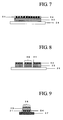
- FIG. 7 One example where a dicing tape is adhered to a backside or grinding side of the wafer after grinding is shown in Figure 7, wherein only a stripping sheet 22 is removed from the resin sheet, and a dicing tape 25 is adhered to a backside of the wafer 23.
- the removal of the stripping sheet 22 is carried out by using, for instance, "HR-8500-II" commercially available from Nitto Denko Co., Ltd.
- the dicing tape 25 usable in this embodiment is not particularly limited, as long as the dicing tape is one which is usually used in the field of art.
- the devices and conditions for adhering the dicing tape 25 are not particularly limited, and known devices and conditions can be employed.
- FIG 8 One example after cutting (dicing) of the wafer is shown in Figure 8, wherein the wafer 23 to which the resin composition 21 is adhered is cut into individual chips 26 with keeping the wafer 23 adhered to the dicing tape 25.
- the cutting of the wafer is not particularly limited, and cutting is carried out with an ordinary dicing device.
- FIG. 9 One example after mounting the chips is shown in Figure 9, wherein the individual chips 26 are removed from the dicing tape, and mounted on a printed circuit board 27.
- the gap formed between the wafer 23 and the printed circuit board 27 is resin-encapsulated by the resin composition.
- the printed circuit board 27 is the same one used in Embodiment 1.
- the method for mounting individual chips 26 on a printed circuit board 27 includes a method comprising firstly picking up and removing the individual chips 26 from a dicing tape 25, and housing the individual chips in a chip tray or conveying the individual chips 26 to a chip-mounting nozzle of a flip-chip bonder; and thereafter (i) obtaining electric connection at the same time as mounting the individual chips 26 to the printed circuit board 27, while pressing with heating in a bump-bonding form; (ii) obtaining an electric connection at the same time as mounting the individual chips 26 to a printed circuit board 27 using heat, pressure and ultrasonication; (iii) mounting the individual chips 26 to a printed circuit board 27, and thereafter obtaining electric connection by solder reflow; and the like.
- the above-mentioned heating temperature is preferably 500°C or lower, more preferably 400°C or lower, from the viewpoint of preventing deterioration of the individual chips 26 and the printed circuit board 27.
- the lower limit of the heating temperature is about 100°C.
- the above-mentioned pressure conditions depend on the number of connecting electrodes or the like, the pressure is preferably from 9.8 ⁇ 10 -3 to 1.96 N/bump, more preferably from 1.96 ⁇ 10 -2 to 9.8 ⁇ 10 -1 N/bump.
- the semiconductor device obtained is encompassed in this embodiment.
- a semiconductor device (equivalent to a semiconductor device shown in Figure 1) was manufactured by using the resin composition prepared above in accordance with the above-mentioned method for manufacturing a semiconductor device. Specifically, a resin composition heated to a temperature of 80°C in a molten state was subjected to potting on a printed circuit board (thickness of a glass epoxy board: 0.8 mm).
- the resin in a molten state was filled into a gap between the printed circuit board and the semiconductor element. Thereafter, the soldering was carried out under the following JEDEC condition with a solder-reflow furnace (commercially available from JARD, Inc., trade name: MJ-R4000) to provide an electric connection.
- JEDEC condition with a solder-reflow furnace (commercially available from JARD, Inc., trade name: MJ-R4000) to provide an electric connection.
- IPC/JEDEC J-STD-20C reflow condition for Sn-Pb was used.
- the temperature profile was as follows: Ramping up for preheat from 25° to 100°C in 60 seconds, keeping the temperature for flux activation between 100° and 150°C for 90 seconds, following ramping up to 240°C by an averaging rate of 2°C/second, keeping within 5°C of actual peak temperature 240°C for 15 seconds, and finally ramping down cooling by less than 6°C/second.
- the time maintained above 183°C (solder melting temperature) was 90 seconds.
- the resin was then cured in the oven (PHH-100, commercially available from ESPEC Corporation) at a temperature of 170°C for 120 minutes to manufacture an intended semiconductor device.
- the semiconductor device obtained was evaluated as described above. The results are shown in Tables 3 and 4. Example Nos.
- a procedure of keeping the semiconductor device at -55°C for 10 minutes, and thereafter keeping the semiconductor device at 125°C for 10 minutes was carried out for 500 times (TST 500 cycles) or 1000 times (TST 1000 cycles). Thereafter, the electric resistance of the semiconductor device was determined with a daisy chain (commercially available from ADVANTEST, trade name: DIGITAL MULTIMETER TR6847). The obtained electric resistance was compared to the initial value (electric resistance of the semiconductor device before carrying out the above-mentioned procedure). Those semiconductor devices of which electric resistances are twice or more of the initial value were counted as defective products.
- the resin composition prepared above was adhered to ethyl vinyl acetate (stripping sheet, 135 ⁇ m) at 80°C, to form a resin sheet.
- This resin sheet was adhered to a semiconductor circuit board side of the bump-mounting wafer with a roller adhering apparatus (commercially available from Nitto Denko Co., Ltd., trade name: DR-8500-II) at 70°C.
- a dicing tape (commercially available from Nitto Denko Co., Ltd., trade name: DU-300) was adhered to the wafer obtained.
- the stripping sheet was removed, and thereafter the wafer obtained was cut into individual chips with a dicing apparatus (commercially available from DISCO, trade name: DFD-651), to give a chip with the resin composition.
- the resin composition prepared in Comparative Example 2-1 had a high transmittance and a low viscosity, so that a chip with the resin composition could be obtained. Since the resin composition has a high coefficient of linear thermal expansion, the semiconductor device produced therefrom caused failure in TST500 and TST1000. In addition, since the resin compositions prepared in Comparative Examples 2-2, 2-4 and 2-5 had high viscosities and little fluidity, the adhesion to the wafer at a given temperature could not be made, so that the chips with the resin composition could not be obtained. In addition, since the resin compositions prepared in Comparative Examples 2-3 and 2-5 had low transmittances that were not pattern-recognizable, the chips with the resin composition could not be obtained.
- the semiconductor devices produced in Examples 2-1 to 2-5 retained pattern-recognizable transmittance, had fluidity capable of adhering to the wafer, and secured stable electric resistance in a thermal shock test, i.e. the semiconductor devices are excellent in electric connection reliability.
- the resin composition for encapsulating a semiconductor of the present invention can be utilized in encapsulating a gap formed between a printed circuit board and a semiconductor element in the semiconductor industries.
Applications Claiming Priority (4)
| Application Number | Priority Date | Filing Date | Title |
|---|---|---|---|
| JP2004013405 | 2004-01-21 | ||
| JP2004013405A JP4417122B2 (ja) | 2004-01-21 | 2004-01-21 | シート状半導体封止用樹脂組成物 |
| JP2004013396 | 2004-01-21 | ||
| JP2004013396A JP2005206664A (ja) | 2004-01-21 | 2004-01-21 | 半導体封止用樹脂組成物 |
Publications (1)
| Publication Number | Publication Date |
|---|---|
| EP1557880A1 true EP1557880A1 (de) | 2005-07-27 |
Family
ID=34635686
Family Applications (1)
| Application Number | Title | Priority Date | Filing Date |
|---|---|---|---|
| EP20050000896 Withdrawn EP1557880A1 (de) | 2004-01-21 | 2005-01-18 | Harzzusammensetzung um Halbleiter zu verkapseln |
Country Status (4)
| Country | Link |
|---|---|
| US (1) | US20050158557A1 (de) |
| EP (1) | EP1557880A1 (de) |
| KR (1) | KR101139740B1 (de) |
| TW (1) | TWI369716B (de) |
Cited By (3)
| Publication number | Priority date | Publication date | Assignee | Title |
|---|---|---|---|---|
| WO2006049853A2 (en) * | 2004-11-01 | 2006-05-11 | 3M Innovative Properties Company | Method of connecting a semiconductor package to a printed wiring board |
| EP2166037A1 (de) * | 2007-07-11 | 2010-03-24 | Nissan Chemical Industries, Ltd. | Epoxidharzformendes flüssigpräparat mit anorganischen partikeln |
| WO2016050557A1 (de) * | 2014-09-30 | 2016-04-07 | Siemens Aktiengesellschaft | Formulierung für ein isoliersystem und isoliersystem |
Families Citing this family (11)
| Publication number | Priority date | Publication date | Assignee | Title |
|---|---|---|---|---|
| JP2008192984A (ja) * | 2007-02-07 | 2008-08-21 | Elpida Memory Inc | 半導体装置及びその製造方法 |
| JP4430085B2 (ja) * | 2007-03-01 | 2010-03-10 | 日東電工株式会社 | ダイシング・ダイボンドフィルム |
| EP2242090A4 (de) * | 2008-02-07 | 2011-05-18 | Sumitomo Bakelite Co | Folie für halbleiter, verfahren zur herstellung eines halbleiterbauelements und halbleiterbauelement |
| EP2246979A4 (de) * | 2008-02-18 | 2014-03-05 | Murata Manufacturing Co | Elastische wellenvorrichtung und herstellungsverfahren dafür |
| JP4801127B2 (ja) * | 2008-09-01 | 2011-10-26 | 日東電工株式会社 | ダイシング・ダイボンドフィルムの製造方法 |
| US20100244286A1 (en) * | 2008-10-06 | 2010-09-30 | Lagsa Earl Vincent B | Nanocomposites for optoelectronic devices |
| JP5234029B2 (ja) * | 2009-08-05 | 2013-07-10 | 山栄化学株式会社 | 無洗浄活性樹脂組成物及び表面実装技術 |
| DE102010032555A1 (de) * | 2010-07-29 | 2012-02-02 | Siemens Aktiengesellschaft | Isolierung für rotierende elektrische Maschinen |
| DE102012205650A1 (de) | 2012-04-05 | 2013-10-10 | Siemens Aktiengesellschaft | Isolierstoff für rotierende Maschinen |
| JP6135991B2 (ja) * | 2012-10-11 | 2017-05-31 | パナソニックIpマネジメント株式会社 | 封止用エポキシ樹脂無機複合シート |
| KR101922296B1 (ko) * | 2016-06-23 | 2018-11-26 | 삼성에스디아이 주식회사 | 고체상 반도체 소자 밀봉용 에폭시 수지 조성물 및 이를 포함하는 봉지재 및 반도체 패키지 |
Citations (7)
| Publication number | Priority date | Publication date | Assignee | Title |
|---|---|---|---|---|
| JPS63297436A (ja) * | 1987-05-28 | 1988-12-05 | Mitsubishi Kasei Corp | Ic用封止材樹脂組成物 |
| JPH10168286A (ja) * | 1996-12-13 | 1998-06-23 | Nitto Denko Corp | 硬化促進剤含有マイクロカプセルおよびそれを用いた熱硬化性樹脂組成物ならびに半導体装置 |
| JP2000063494A (ja) * | 1998-08-20 | 2000-02-29 | Toshiba Chem Corp | エポキシ樹脂組成物および半導体封止装置 |
| EP1090942A1 (de) * | 1999-10-06 | 2001-04-11 | Nitto Denko Corporation | Harzzusammensetzung zur Einkapselung von Halbleitern, Halbleiteranordnungen die diese enthalten und Verfahren für die Herstellung von diesen Halbleiteranordnungen |
| US20030017342A1 (en) * | 2001-04-06 | 2003-01-23 | Koichiro Nakamura | Optical adhesive composition and optical device |
| JP2003096268A (ja) * | 2001-09-19 | 2003-04-03 | Sumitomo Bakelite Co Ltd | エポキシ樹脂組成物及び半導体装置 |
| US20030069331A1 (en) * | 2000-02-15 | 2003-04-10 | Inada Teiichi | Adhesive composition , process for producing the same, adhesive film made with the same, substrate for semiconductor mounting, and semiconductor device |
Family Cites Families (4)
| Publication number | Priority date | Publication date | Assignee | Title |
|---|---|---|---|---|
| JP3294803B2 (ja) * | 1997-08-18 | 2002-06-24 | 株式会社日本触媒 | 熱硬化性樹脂封止材 |
| JP2000336247A (ja) * | 1999-05-27 | 2000-12-05 | C I Kasei Co Ltd | 液状エポキシ樹脂封止材 |
| EP1236765A1 (de) * | 2001-02-28 | 2002-09-04 | hanse chemie GmbH | Siliciumdioxiddispersion |
| US20040101688A1 (en) * | 2002-11-22 | 2004-05-27 | Slawomir Rubinsztajn | Curable epoxy compositions, methods and articles made therefrom |
-
2005
- 2005-01-18 EP EP20050000896 patent/EP1557880A1/de not_active Withdrawn
- 2005-01-19 KR KR1020050004897A patent/KR101139740B1/ko active IP Right Grant
- 2005-01-19 US US11/037,051 patent/US20050158557A1/en not_active Abandoned
- 2005-01-21 TW TW094101867A patent/TWI369716B/zh not_active IP Right Cessation
Patent Citations (7)
| Publication number | Priority date | Publication date | Assignee | Title |
|---|---|---|---|---|
| JPS63297436A (ja) * | 1987-05-28 | 1988-12-05 | Mitsubishi Kasei Corp | Ic用封止材樹脂組成物 |
| JPH10168286A (ja) * | 1996-12-13 | 1998-06-23 | Nitto Denko Corp | 硬化促進剤含有マイクロカプセルおよびそれを用いた熱硬化性樹脂組成物ならびに半導体装置 |
| JP2000063494A (ja) * | 1998-08-20 | 2000-02-29 | Toshiba Chem Corp | エポキシ樹脂組成物および半導体封止装置 |
| EP1090942A1 (de) * | 1999-10-06 | 2001-04-11 | Nitto Denko Corporation | Harzzusammensetzung zur Einkapselung von Halbleitern, Halbleiteranordnungen die diese enthalten und Verfahren für die Herstellung von diesen Halbleiteranordnungen |
| US20030069331A1 (en) * | 2000-02-15 | 2003-04-10 | Inada Teiichi | Adhesive composition , process for producing the same, adhesive film made with the same, substrate for semiconductor mounting, and semiconductor device |
| US20030017342A1 (en) * | 2001-04-06 | 2003-01-23 | Koichiro Nakamura | Optical adhesive composition and optical device |
| JP2003096268A (ja) * | 2001-09-19 | 2003-04-03 | Sumitomo Bakelite Co Ltd | エポキシ樹脂組成物及び半導体装置 |
Non-Patent Citations (4)
| Title |
|---|
| PATENT ABSTRACTS OF JAPAN vol. 013, no. 134 (C - 581) 4 April 1989 (1989-04-04) * |
| PATENT ABSTRACTS OF JAPAN vol. 1998, no. 11 30 September 1998 (1998-09-30) * |
| PATENT ABSTRACTS OF JAPAN vol. 2000, no. 05 14 September 2000 (2000-09-14) * |
| PATENT ABSTRACTS OF JAPAN vol. 2003, no. 08 6 August 2003 (2003-08-06) * |
Cited By (5)
| Publication number | Priority date | Publication date | Assignee | Title |
|---|---|---|---|---|
| WO2006049853A2 (en) * | 2004-11-01 | 2006-05-11 | 3M Innovative Properties Company | Method of connecting a semiconductor package to a printed wiring board |
| WO2006049853A3 (en) * | 2004-11-01 | 2006-08-24 | 3M Innovative Properties Co | Method of connecting a semiconductor package to a printed wiring board |
| EP2166037A1 (de) * | 2007-07-11 | 2010-03-24 | Nissan Chemical Industries, Ltd. | Epoxidharzformendes flüssigpräparat mit anorganischen partikeln |
| EP2166037A4 (de) * | 2007-07-11 | 2012-07-25 | Nissan Chemical Ind Ltd | Epoxidharzformendes flüssigpräparat mit anorganischen partikeln |
| WO2016050557A1 (de) * | 2014-09-30 | 2016-04-07 | Siemens Aktiengesellschaft | Formulierung für ein isoliersystem und isoliersystem |
Also Published As
| Publication number | Publication date |
|---|---|
| US20050158557A1 (en) | 2005-07-21 |
| KR20050076660A (ko) | 2005-07-26 |
| TWI369716B (en) | 2012-08-01 |
| TW200537578A (en) | 2005-11-16 |
| KR101139740B1 (ko) | 2012-04-26 |
Similar Documents
| Publication | Publication Date | Title |
|---|---|---|
| EP1557880A1 (de) | Harzzusammensetzung um Halbleiter zu verkapseln | |
| EP1233446B1 (de) | Thermisch aushärtbare Harzverbindung und Halbleitervorrichtung, die dieselbe verwendet | |
| US7521122B2 (en) | Laminated sheet | |
| US7312104B2 (en) | Resin composition for encapsulating semiconductor device | |
| KR102012790B1 (ko) | 반도체 장치 및 반도체 장치의 제조 방법 | |
| US20120205820A1 (en) | Encapsulating resin sheet and semiconductor device using the same, and manufacturing method for the semiconductor device | |
| KR102012788B1 (ko) | 접착 필름, 반도체 장치의 제조 방법 및 반도체 장치 | |
| US20150014842A1 (en) | Semiconductor device and production method therefor | |
| JP4417122B2 (ja) | シート状半導体封止用樹脂組成物 | |
| JP4206631B2 (ja) | 熱硬化性液状封止樹脂組成物、半導体素子の組立方法及び半導体装置 | |
| CN100543099C (zh) | 半导体密封用树脂组合物 | |
| JP2001223227A (ja) | 半導体封止用樹脂組成物および半導体装置 | |
| JP2002241617A (ja) | 熱硬化性樹脂組成物および半導体装置 | |
| JP3938502B2 (ja) | 液状封止樹脂組成物、半導体素子の組立方法及び半導体装置 | |
| JP3732148B2 (ja) | 半導体装置の製造方法及び半導体装置 | |
| US20150035175A1 (en) | Adhesive for semiconductor, fluxing agent, manufacturing method for semiconductor device, and semiconductor device | |
| JP3779091B2 (ja) | 封止用樹脂組成物 | |
| KR20210143720A (ko) | 반도체용 접착제, 반도체 장치의 제조 방법 및 반도체 장치 | |
| JPH0855867A (ja) | 樹脂封止型半導体装置 | |
| JP2000174044A (ja) | 半導体素子の組立方法 | |
| KR102204964B1 (ko) | 반도체 회로 접속용 접착제 조성물 및 이를 포함한 접착 필름 | |
| JP2000195904A (ja) | 半導体素子の組立方法 | |
| KR20220015197A (ko) | 반도체 회로 접속용 접착제 조성물 및 이를 포함한 반도체 회로 접속용 접착 필름 | |
| US8772176B2 (en) | Method for forming an adhesive layer and adhesive composition | |
| KR20220011938A (ko) | 반도체 회로 접속용 접착제 조성물 및 이를 포함한 반도체 회로 접속용 접착 필름 |
Legal Events
| Date | Code | Title | Description |
|---|---|---|---|
| PUAI | Public reference made under article 153(3) epc to a published international application that has entered the european phase |
Free format text: ORIGINAL CODE: 0009012 |
|
| AK | Designated contracting states |
Kind code of ref document: A1 Designated state(s): AT BE BG CH CY CZ DE DK EE ES FI FR GB GR HU IE IS IT LI LT LU MC NL PL PT RO SE SI SK TR |
|
| AX | Request for extension of the european patent |
Extension state: AL BA HR LV MK YU |
|
| 17P | Request for examination filed |
Effective date: 20050922 |
|
| AKX | Designation fees paid |
Designated state(s): AT BE BG CH CY CZ DE DK EE ES FI FR GB GR HU IE IS IT LI LT LU MC NL PL PT RO SE SI SK TR |
|
| STAA | Information on the status of an ep patent application or granted ep patent |
Free format text: STATUS: THE APPLICATION HAS BEEN WITHDRAWN |
|
| 18W | Application withdrawn |
Effective date: 20091118 |