EP1540828B1 - Codierung von informationen in integrierten schaltungen - Google Patents
Codierung von informationen in integrierten schaltungen Download PDFInfo
- Publication number
- EP1540828B1 EP1540828B1 EP03795107A EP03795107A EP1540828B1 EP 1540828 B1 EP1540828 B1 EP 1540828B1 EP 03795107 A EP03795107 A EP 03795107A EP 03795107 A EP03795107 A EP 03795107A EP 1540828 B1 EP1540828 B1 EP 1540828B1
- Authority
- EP
- European Patent Office
- Prior art keywords
- signal
- signals
- delay
- paths
- propagating
- Prior art date
- Legal status (The legal status is an assumption and is not a legal conclusion. Google has not performed a legal analysis and makes no representation as to the accuracy of the status listed.)
- Expired - Lifetime
Links
Images


Classifications
-
- H—ELECTRICITY
- H04—ELECTRIC COMMUNICATION TECHNIQUE
- H04L—TRANSMISSION OF DIGITAL INFORMATION, e.g. TELEGRAPHIC COMMUNICATION
- H04L25/00—Baseband systems
- H04L25/02—Details ; arrangements for supplying electrical power along data transmission lines
- H04L25/0264—Arrangements for coupling to transmission lines
- H04L25/0266—Arrangements for providing Galvanic isolation, e.g. by means of magnetic or capacitive coupling
-
- H—ELECTRICITY
- H03—ELECTRONIC CIRCUITRY
- H03M—CODING; DECODING; CODE CONVERSION IN GENERAL
- H03M5/00—Conversion of the form of the representation of individual digits
- H03M5/02—Conversion to or from representation by pulses
-
- G—PHYSICS
- G01—MEASURING; TESTING
- G01R—MEASURING ELECTRIC VARIABLES; MEASURING MAGNETIC VARIABLES
- G01R31/00—Arrangements for testing electric properties; Arrangements for locating electric faults; Arrangements for electrical testing characterised by what is being tested not provided for elsewhere
- G01R31/28—Testing of electronic circuits, e.g. by signal tracer
- G01R31/317—Testing of digital circuits
- G01R31/3181—Functional testing
- G01R31/3185—Reconfiguring for testing, e.g. LSSD, partitioning
- G01R31/318533—Reconfiguring for testing, e.g. LSSD, partitioning using scanning techniques, e.g. LSSD, Boundary Scan, JTAG
- G01R31/318536—Scan chain arrangements, e.g. connections, test bus, analog signals
- G01R31/318538—Topological or mechanical aspects
-
- H—ELECTRICITY
- H01—ELECTRIC ELEMENTS
- H01L—SEMICONDUCTOR DEVICES NOT COVERED BY CLASS H10
- H01L23/00—Details of semiconductor or other solid state devices
- H01L23/52—Arrangements for conducting electric current within the device in operation from one component to another, i.e. interconnections, e.g. wires, lead frames
- H01L23/522—Arrangements for conducting electric current within the device in operation from one component to another, i.e. interconnections, e.g. wires, lead frames including external interconnections consisting of a multilayer structure of conductive and insulating layers inseparably formed on the semiconductor body
- H01L23/5227—Inductive arrangements or effects of, or between, wiring layers
-
- H—ELECTRICITY
- H01—ELECTRIC ELEMENTS
- H01L—SEMICONDUCTOR DEVICES NOT COVERED BY CLASS H10
- H01L2924/00—Indexing scheme for arrangements or methods for connecting or disconnecting semiconductor or solid-state bodies as covered by H01L24/00
- H01L2924/0001—Technical content checked by a classifier
- H01L2924/0002—Not covered by any one of groups H01L24/00, H01L24/00 and H01L2224/00
Definitions
- the present invention relates to a method for coding information in an electronic circuit and an electronic circuit for coding information, said circuit comprising at least two electrically coupled signal paths.
- Cross-talk A well-known electrical phenomenon known as cross-talk exists among signal paths that are electrically coupled to each other.
- Cross-talk manifests itself by inducing voltage glitches on electrically coupled signal paths, which is seen as an undesired disturbance that has to be minimized.
- Cross-talk also manifests itself by modifying the speed of the signals travelling on these signal paths. Normally, neighboring signal paths will affect each other to a greater extent than paths located some distance away from each other, since the closer they are located to each other, the stronger the electrical coupling will be.
- GB 2,089,122 discloses a semiconductor integrated circuit (IC) and seeks to reduce interference between signal lines thereof.
- IC semiconductor integrated circuit
- the first signal line transmits a first signal
- the third signal line transmits a third signal having a phase which is opposite to that of the first signal.
- the cross-talk from the first signal line to the second signal line can be cancelled by the cross-talk from the third signal line to the second signal line, on which a second signal is transmitted.
- This object is achieved by the invention in a first aspect in the form of a method for coding information in an electronic circuit, said circuit comprising at least two electrically coupled signal paths according to claim 1 and in a second aspect in the form of an electronic circuit for coding information, said circuit comprising at least two electrically coupled signal paths according to claim 5.
- This has the advantage that cross-talk related additional hardware is utilized to generate useful information rather than to merely eliminate or reduce an effect that will become more and more pronounced with increasing integration densities on ICs. So, in accordance with the invention, cross-talk is being utilized rather than being countered.
- a method for coding information wherein the relative delay between signals propagating on at least two electrically coupled paths is determined when the signals make a transition from a first logic level to a second logic level. An output signal is then produced having a further logic level depending on the relative delay between the signals.
- an electronic circuit for coding information comprising means arranged to determine the relative delay between signals propagating on at least two electrically coupled paths when the signals make a transition from a first logic level to a second logic level.
- the electronic circuit further comprises means arranged to produce an output signal having a further logic level depending on the relative delay between the signals.
- the invention is based on the idea that cross-talk between two electrically coupled signal paths can be utilized to perform a logical computation.
- a signal is propagating on two signal paths in the form of either rising or falling transitions.
- the relative delay between the transitions on the two paths determines the further logic value i.e., a logic "0" or a logic "1", of the output signal to be produced. This is hereinafter referred to as "delay coding". If the signal on the first path propagates faster than the signal on the second path, an output signal of a first further logic value is produced. If the signal on the second path propagates faster than the signal on the first path, an output signal of a second further logic value is produced.
- logic gates performing computation by means of cross-talk, which is used to modify the speed of transitions propagating on electrically coupled signal paths and thus modulating delays.
- cross-talk is used to modify the speed of transitions propagating on electrically coupled signal paths and thus modulating delays.
- logic gates comprised of transistors can be replaced by logic gates comprised of electrically coupled signal paths.
- Transistors are only needed when conversion is to be done between the boolean domain, where signal values are represented by logic levels, and the delay domain where signal values are represented by the difference in arrival time of signals.
- a logical signal is divided into two delay coded signals propagating on respective electrically coupled signal paths.
- a relative delay between the two delay coded signals is created by means of a delay encoder, e.g. a programmable delay circuit, a buffer or some other type of circuit having an inherent delay.
- a delay encoder e.g. a programmable delay circuit, a buffer or some other type of circuit having an inherent delay.
- the conversion between the boolean domain, i.e., the standard digital binary domain, and the delay coding domain is performed.
- Standard delay decoders for example metastability filters, can be used to convert delay coded signals to binary signals.
- Fig. 1 shows an embodiment of delay coding according to the invention.
- two signal paths X0, X1 are needed for each binary variable X.
- the signal paths X0, X1 are constituted of for example wires, copper lines on a printed circuit board, signal lines in an integrated circuit etc.
- electrical coupling between the signal paths X0, X1 must exist, which usually is the case among neighboring signal paths X0, X1.
- a signal is propagating on both signal paths X0, X1 in the form of either rising or falling transitions.
- the delay coding scheme is the same for falling transitions.
- the further logic value i.e., a logic "1” or "0"
- a logic "1” or "0” that is assigned to the output depending on the relative delay between the signals, i.e., depending on which of the signals propagates faster, is a mere matter of choice, i.e., convention.
- the conventional delay coding scheme shown in Fig. 1 will be used.
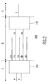
- Fig. 2 shows another embodiment of delay coding according to the invention, in which embodiment an AND gate 200 is implemented.
- the delay encoder 120 and the delay decoder 140 are standard electronic components utilized to make the conversion between the boolean domain I and the delay coding domain II and vice versa.
- variables X and Y are delay coded as described in Fig. 1 .
- the signal propagating on signal path ⁇ is a reference transition synchronized with the fastest signal propagating on either of the signal paths X0, X1, Y0 and Y1.
- Three possible scenarios can occur:
- circuit in Fig. 2 implements an AND gate 200.
- the verb 'to accelerate' is used to indicate the difference between a signal propagation speed on a wire caused by advantageous signal propagations on neighboring wires, and a signal propagation speed on a wire having no advantageous signal propagations on its neighboring wires, leaving the signal propagation on the wire to be more hampered by cross-talk with its environment. Consequently, the signal propagation speed in the first situation is better than the signal propagation speed in the second situation, hence the signal propagation on the wire in the first situation is 'accelerated' with respect to the signal propagation of the wire in the second situation. It is stipulated that the use of the verb 'to accelerate' as used in the aforementioned context should not necessarily be explained as an indication of an increase of the actual speed of a signal propagation on the wire.
- Fig. 4 shows a speed-matching gate 500 employed in the present invention.
- An important factor in interference delay logic is that signals such as the reference have the proper speed, i.e., a well-defined speed. A signal propagating over a wire in a random environment will always exhibit some delay resulting from the interaction of the wire with the environment.
- a wire from an interacting wire pair employing the techniques of the present invention may have a smaller delay than the delay from a random environment, because the cross-talk with the neighboring wire in the wire pair may be reduced due to the fact that both wires may carry matching transient signals.
- Drivers 502 are included in both output terminals 520 and 530 to reduce the load on the wire X1, in order to allow for an optimization of the propagation speed of the signal. Because the switching behavior on output terminal 530 matches the switching behavior on output terminal 520, the cross-talk between the output terminal 520 and its environment is reduced, thus reducing the effects of cross-talk on the output terminal 520, which improves the propagation speed of the signal on output terminal 520.
- Drivers 502 and receiver 504 may be implemented by any buffer or driver known from the art.
- transistors are only needed in the form of delay encoders 120 and delay decoders 140 when conversion is to be done between the boolean domain I, where signal values are represented by logic levels, and the delay coding domain II where signal values are represented by the difference in arrival time of signals.
- the relative number of transistors used in a logical network decreases as the number of cascaded gates increases, since all logical computations can be performed in the delay coding domain II and transistors are necessary only at the interfaces between the two domains I and II.
- An extensive network of delay coded gates would still only need transistors at the interfaces. Possibly, simple transistor buffers, e.g.
- drivers 502 are used to amplify the signals propagating on the signal paths, i.e., output terminals 520 and 530.
- the two wires each have an own driver 502 in order for acceleration to take place. Note that the length of the two wires is a design parameter; the longer the parallel run length of the two wires, the more acceleration is obtained.
- Delay coding can preferably be used in interconnections for electrical signals.
- Interconnections e.g., busses on a printed circuit board, are passive components for transmissions of bits from one place to another.
- Fig. 5 shows a typical bus structure 600 containing flip-flops 1, buffers 2 and wires 3 for amplification of signals propagating on the wires.
- delay coding By using delay coding, logical computations can be performed on the busses while transmitting the signals.
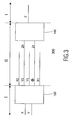
- Fig. 6 shows a circuit 700 implementing an embodiment of delay coding according to the invention when used on a bus structure or another multiple-wire arrangement.
- a data wire 610 is split into a program wire 620 and a signal wire 630.
- computation can only be performed when a transition takes place on the data wire 610.
- the signal wire 630 and the program wire 620 must be electrically coupled to each other in order to employ the effects of cross-talk, i.e., modifying the speed of the signal propagating on the signal wire 630. Synchronization of the program wire 620 and the signal wire 630 is an important issue, since the delay modification caused by the program wire 620 on the signal wire 630 should preferably be maximised.
- a standard delay decoder 140 can be used to convert delay coded signals to binary signals by comparing the transient behavior on signal wire 630 with that of reference wire 640.
- the wires 610, 620, 630, 640 may be equipped with appropriate driver circuits 602 to obtain the desired signal strength on the wires.
- Fig. 7 shows another embodiment of delay coding according to the invention when used on bus structures or other multiple-wire arrangements.
- the circuit 700 in Fig. 6 is represented by a block followed by a repeater 720.
- the block 700 and the repeater 720 forms a stage. Each stage can perform computing and employ data from the previous stages.
- the conventional transmission path for busses includes the signals propagating via "Data" and "Z”.
- Variables a, b, and c represent additional data transportation and Z-EXTRA represents additional computed data transportation. Note that data transport may take place without the performance of computation.
Landscapes
- Engineering & Computer Science (AREA)
- Power Engineering (AREA)
- Physics & Mathematics (AREA)
- General Physics & Mathematics (AREA)
- General Engineering & Computer Science (AREA)
- Microelectronics & Electronic Packaging (AREA)
- Computer Hardware Design (AREA)
- Condensed Matter Physics & Semiconductors (AREA)
- Computer Networks & Wireless Communication (AREA)
- Signal Processing (AREA)
- Theoretical Computer Science (AREA)
- Design And Manufacture Of Integrated Circuits (AREA)
- Compression, Expansion, Code Conversion, And Decoders (AREA)
- Tests Of Electronic Circuits (AREA)
- Pulse Circuits (AREA)
Claims (7)
- Verfahren zum Codieren von Informationen in einer elektronischen Schaltung (700), wobei die Schaltung wenigstens zwei elektrisch gekoppelte Signalwege (620; 630) umfasst, und wobei das Verfahren die Schritte umfasst:Bestimmen einer relativen Verzögerung zwischen Signalen, die sich auf den Wegen (620; 630) fortpflanzen, wenn die Signale einen Übergang von einem ersten logischen Pegel zu einem zweiten logischen Pegel vollziehen; undErzeugen eines Ausgangsignals (Z_EXTRA), das einen weiteren logischen Pegel aufweist, der von der relativen Verzögerung zwischen den Signalen abhängt;gekennzeichnet durch das Manipulieren der relativen Verzögerung durch Modifizieren der Fortpflanzungsgeschwindigkeit eines der Signale.
- Verfahren nach Anspruch 1, das ferner den Schritt umfasst:Unterteilen eines logischen Signals (X, Y) in zwei Signale (X0; X1, Y0; Y1), die sich auf einem entsprechenden der Signalwege (620; 630) fortpflanzen sollen.
- Verfahren nach Anspruch 1 oder 2, wobei der Schritt des Manipulierens der relativen Verzögerung das Erzeugen eines Referenzsignals (Φ) umfasst, das mit dem schnellsten Signal synchronisiert ist, das sich auf einem der Signalwege (620; 630) fortpflanzt.
- Verfahren nach Anspruch 1, wobei der Erzeugungsschritt mittels eines Verzögerungsdecodierers (140) durchgeführt wird.
- Elektronische Schaltung (700) zum Codieren von Informationen, umfassend:wenigstens zwei elektrisch gekoppelte Signalwege (620; 630);Mittel (640) zum Bestimmen einer relativen Verzögerung zwischen Signalen, die sich auf den Wegen (620; 630) fortpflanzen, wenn die Signale einen Übergang von einem ersten logischen Pegel zu einem zweiten logischen Pegel vollziehen;Mittel (140) zum Erzeugen eines Ausgangssignals (Z_EXTRA), das einen weiteren logischen Pegel aufweist, der von der relativen Verzögerung zwischen den zwei Signalen abhängt;gekennzeichnet durch ein weiteres Mittel zum Erzeugen eines Referenzsignals (Φ), das mit dem schnellsten Signal synchronisiert ist, das sich auf einem der Signalwege (620; 630) fortpflanzt, um die Fortpflanzungsgeschwindigkeit eines der Signale zu modifizieren.
- Schaltung nach Anspruch 5, ferner umfassend:Mittel zum Unterteilen eines logischen Signals (X, Y) in zwei Signale (X0; X1, Y0; Y1), die sich auf einem entsprechenden der Signalwege (620; 630) fortpflanzen sollen.
- Schaltung nach Anspruch 5, wobei die Erzeugungsmittel (140) einen Verzögerungsdecodierer umfassen.
Priority Applications (1)
| Application Number | Priority Date | Filing Date | Title |
|---|---|---|---|
| EP03795107A EP1540828B1 (de) | 2002-09-13 | 2003-08-06 | Codierung von informationen in integrierten schaltungen |
Applications Claiming Priority (4)
| Application Number | Priority Date | Filing Date | Title |
|---|---|---|---|
| EP02078779 | 2002-09-13 | ||
| EP02078779 | 2002-09-13 | ||
| PCT/IB2003/003496 WO2004025838A1 (en) | 2002-09-13 | 2003-08-06 | Coding of information in integrated circuits |
| EP03795107A EP1540828B1 (de) | 2002-09-13 | 2003-08-06 | Codierung von informationen in integrierten schaltungen |
Publications (2)
| Publication Number | Publication Date |
|---|---|
| EP1540828A1 EP1540828A1 (de) | 2005-06-15 |
| EP1540828B1 true EP1540828B1 (de) | 2009-02-25 |
Family
ID=31985093
Family Applications (1)
| Application Number | Title | Priority Date | Filing Date |
|---|---|---|---|
| EP03795107A Expired - Lifetime EP1540828B1 (de) | 2002-09-13 | 2003-08-06 | Codierung von informationen in integrierten schaltungen |
Country Status (10)
| Country | Link |
|---|---|
| US (1) | US7515074B2 (de) |
| EP (1) | EP1540828B1 (de) |
| JP (1) | JP2005538632A (de) |
| KR (1) | KR20050043945A (de) |
| CN (1) | CN100481731C (de) |
| AT (1) | ATE424060T1 (de) |
| AU (1) | AU2003255884A1 (de) |
| DE (1) | DE60326363D1 (de) |
| TW (1) | TWI310594B (de) |
| WO (1) | WO2004025838A1 (de) |
Families Citing this family (1)
| Publication number | Priority date | Publication date | Assignee | Title |
|---|---|---|---|---|
| US8145442B2 (en) * | 2009-01-30 | 2012-03-27 | Synopsys, Inc. | Fast and accurate estimation of gate output loading |
Citations (1)
| Publication number | Priority date | Publication date | Assignee | Title |
|---|---|---|---|---|
| EP1286470A2 (de) * | 2001-07-19 | 2003-02-26 | Fujitsu Limited | Eingangs-/Ausgangsschnittstelle und Integrierte Halbleiterschaltung mit Eingangs-/Ausgangsschnittstelle |
Family Cites Families (19)
| Publication number | Priority date | Publication date | Assignee | Title |
|---|---|---|---|---|
| US3084223A (en) * | 1960-12-23 | 1963-04-02 | Bell Telephone Labor Inc | Crosstalk reduction in plural carrier multiplex systems |
| JPS5140449A (ja) * | 1974-10-04 | 1976-04-05 | Toray Industries | Makitorisochi |
| JPS5784149A (en) * | 1980-11-14 | 1982-05-26 | Hitachi Ltd | Semiconductor integrated circuit device |
| JPS604347A (ja) * | 1983-06-22 | 1985-01-10 | Fuji Xerox Co Ltd | デイジタル信号伝送システムの障害対策方式 |
| US5493588A (en) * | 1992-01-22 | 1996-02-20 | Trimble Navigation Limited | Multipath compensation for code phase signals |
| JP3136742B2 (ja) * | 1992-02-14 | 2001-02-19 | 日産自動車株式会社 | 通信装置 |
| IL120538A (en) * | 1997-03-26 | 2000-11-21 | Dspc Tech Ltd | Method and apparatus for reducing spread-spectrum noise |
| US6148038A (en) * | 1997-03-31 | 2000-11-14 | Sun Microsystems, Inc. | Circuit for detecting and decoding phase encoded digital serial data |
| US6480548B1 (en) * | 1997-11-17 | 2002-11-12 | Silicon Graphics, Inc. | Spacial derivative bus encoder and decoder |
| WO1999046861A1 (en) * | 1998-03-11 | 1999-09-16 | Thomson Licensing S.A. | Digital signal modulation system |
| JP3137328B2 (ja) * | 1998-04-22 | 2001-02-19 | 富士通株式会社 | ノイズ除去方法および伝送回路 |
| US6731622B1 (en) * | 1998-05-01 | 2004-05-04 | Telefonaktiebolaget Lm Ericsson (Publ) | Multipath propagation delay determining means using periodically inserted pilot symbols |
| JP2001326584A (ja) * | 2000-05-18 | 2001-11-22 | Nec Corp | パス検出方式と受信装置 |
| KR100335503B1 (ko) * | 2000-06-26 | 2002-05-08 | 윤종용 | 서로 다른 지연 특성을 동일하게 하는 신호 전달 회로,신호 전달 방법 및 이를 구비하는 반도체 장치의 데이터래치 회로 |
| JP3813490B2 (ja) * | 2001-10-30 | 2006-08-23 | 富士通株式会社 | スペクトラム拡散レイク受信機 |
| JP2003316736A (ja) * | 2002-04-19 | 2003-11-07 | Oki Electric Ind Co Ltd | Usb回路およびデータ構造 |
| US6958721B2 (en) * | 2003-09-18 | 2005-10-25 | The Regents Of The University Of Colorado | Matched delay line voltage converter |
| JP3927576B2 (ja) * | 2005-01-31 | 2007-06-13 | 富士通株式会社 | 入出力インタフェースおよび半導体集積回路 |
| US20070271535A1 (en) * | 2006-05-16 | 2007-11-22 | National Tsing Hua University | Method for crosstalk elimination and bus architecture performing the same |
-
2003
- 2003-08-06 EP EP03795107A patent/EP1540828B1/de not_active Expired - Lifetime
- 2003-08-06 CN CNB038217961A patent/CN100481731C/zh not_active Expired - Fee Related
- 2003-08-06 KR KR1020057004206A patent/KR20050043945A/ko not_active Ceased
- 2003-08-06 AT AT03795107T patent/ATE424060T1/de not_active IP Right Cessation
- 2003-08-06 DE DE60326363T patent/DE60326363D1/de not_active Expired - Lifetime
- 2003-08-06 AU AU2003255884A patent/AU2003255884A1/en not_active Abandoned
- 2003-08-06 WO PCT/IB2003/003496 patent/WO2004025838A1/en not_active Ceased
- 2003-08-06 US US10/527,551 patent/US7515074B2/en not_active Expired - Lifetime
- 2003-08-06 JP JP2004535729A patent/JP2005538632A/ja active Pending
- 2003-09-10 TW TW092125072A patent/TWI310594B/zh not_active IP Right Cessation
Patent Citations (1)
| Publication number | Priority date | Publication date | Assignee | Title |
|---|---|---|---|---|
| EP1286470A2 (de) * | 2001-07-19 | 2003-02-26 | Fujitsu Limited | Eingangs-/Ausgangsschnittstelle und Integrierte Halbleiterschaltung mit Eingangs-/Ausgangsschnittstelle |
Also Published As
| Publication number | Publication date |
|---|---|
| TW200419734A (en) | 2004-10-01 |
| CN1682447A (zh) | 2005-10-12 |
| TWI310594B (en) | 2009-06-01 |
| KR20050043945A (ko) | 2005-05-11 |
| AU2003255884A1 (en) | 2004-04-30 |
| US20050270194A1 (en) | 2005-12-08 |
| US7515074B2 (en) | 2009-04-07 |
| CN100481731C (zh) | 2009-04-22 |
| DE60326363D1 (de) | 2009-04-09 |
| EP1540828A1 (de) | 2005-06-15 |
| ATE424060T1 (de) | 2009-03-15 |
| JP2005538632A (ja) | 2005-12-15 |
| WO2004025838A1 (en) | 2004-03-25 |
Similar Documents
| Publication | Publication Date | Title |
|---|---|---|
| US6711089B2 (en) | Method and apparatus for performing signal synchronization | |
| EP1540828B1 (de) | Codierung von informationen in integrierten schaltungen | |
| KR100209224B1 (ko) | 고속 다중화기 | |
| KR100678332B1 (ko) | 데이터 종속 구동 강도 제어 로직을 구비한 버스 드라이버 | |
| US6642748B2 (en) | Input circuit | |
| US6690221B1 (en) | Method and apparatus to delay signal latching | |
| KR20020017082A (ko) | 버스라인들 간의 스큐를 방지하기 위한 메모리 모듈 | |
| US7492205B2 (en) | Clock generator | |
| US6144224A (en) | Clock distribution network with dual wire routing | |
| JP3198999B2 (ja) | スキャンパス回路のクロックツリー形成方法 | |
| JPH0437447B2 (de) | ||
| JPH11340796A (ja) | フリップフロップ回路 | |
| JP2600597B2 (ja) | 情報伝播用ダイナミック回路 | |
| GB2307365A (en) | A transparent latch immune to control signal race hazard | |
| JPS62217632A (ja) | 半導体集積回路 | |
| KR0154723B1 (ko) | 클럭신호 입력회로 | |
| KR0158640B1 (ko) | 데이타 버스 제어회로 | |
| JPH0675658A (ja) | 半導体集積回路 | |
| JPH08307460A (ja) | デジタル信号伝送路 | |
| JPH01166968A (ja) | 論理装置 | |
| JPH02285708A (ja) | フリップフロップic | |
| JPH11330374A (ja) | 半導体集積回路装置 | |
| JPH09331260A (ja) | 半導体装置 | |
| JPH04222995A (ja) | シフトレジスタ回路 | |
| JPH0370414B2 (de) |
Legal Events
| Date | Code | Title | Description |
|---|---|---|---|
| PUAI | Public reference made under article 153(3) epc to a published international application that has entered the european phase |
Free format text: ORIGINAL CODE: 0009012 |
|
| 17P | Request for examination filed |
Effective date: 20050413 |
|
| AK | Designated contracting states |
Kind code of ref document: A1 Designated state(s): AT BE BG CH CY CZ DE DK EE ES FI FR GB GR HU IE IT LI LU MC NL PT RO SE SI SK TR |
|
| AX | Request for extension of the european patent |
Extension state: AL LT LV MK |
|
| DAX | Request for extension of the european patent (deleted) | ||
| 17Q | First examination report despatched |
Effective date: 20060110 |
|
| RAP1 | Party data changed (applicant data changed or rights of an application transferred) |
Owner name: NXP B.V. |
|
| GRAP | Despatch of communication of intention to grant a patent |
Free format text: ORIGINAL CODE: EPIDOSNIGR1 |
|
| GRAS | Grant fee paid |
Free format text: ORIGINAL CODE: EPIDOSNIGR3 |
|
| GRAA | (expected) grant |
Free format text: ORIGINAL CODE: 0009210 |
|
| AK | Designated contracting states |
Kind code of ref document: B1 Designated state(s): AT BE BG CH CY CZ DE DK EE ES FI FR GB GR HU IE IT LI LU MC NL PT RO SE SI SK TR |
|
| REG | Reference to a national code |
Ref country code: GB Ref legal event code: FG4D |
|
| REG | Reference to a national code |
Ref country code: CH Ref legal event code: EP |
|
| REG | Reference to a national code |
Ref country code: IE Ref legal event code: FG4D |
|
| REF | Corresponds to: |
Ref document number: 60326363 Country of ref document: DE Date of ref document: 20090409 Kind code of ref document: P |
|
| PG25 | Lapsed in a contracting state [announced via postgrant information from national office to epo] |
Ref country code: FI Free format text: LAPSE BECAUSE OF FAILURE TO SUBMIT A TRANSLATION OF THE DESCRIPTION OR TO PAY THE FEE WITHIN THE PRESCRIBED TIME-LIMIT Effective date: 20090225 Ref country code: SI Free format text: LAPSE BECAUSE OF FAILURE TO SUBMIT A TRANSLATION OF THE DESCRIPTION OR TO PAY THE FEE WITHIN THE PRESCRIBED TIME-LIMIT Effective date: 20090225 Ref country code: NL Free format text: LAPSE BECAUSE OF FAILURE TO SUBMIT A TRANSLATION OF THE DESCRIPTION OR TO PAY THE FEE WITHIN THE PRESCRIBED TIME-LIMIT Effective date: 20090225 |
|
| NLV1 | Nl: lapsed or annulled due to failure to fulfill the requirements of art. 29p and 29m of the patents act | ||
| PG25 | Lapsed in a contracting state [announced via postgrant information from national office to epo] |
Ref country code: AT Free format text: LAPSE BECAUSE OF FAILURE TO SUBMIT A TRANSLATION OF THE DESCRIPTION OR TO PAY THE FEE WITHIN THE PRESCRIBED TIME-LIMIT Effective date: 20090225 Ref country code: SE Free format text: LAPSE BECAUSE OF FAILURE TO SUBMIT A TRANSLATION OF THE DESCRIPTION OR TO PAY THE FEE WITHIN THE PRESCRIBED TIME-LIMIT Effective date: 20090525 |
|
| PG25 | Lapsed in a contracting state [announced via postgrant information from national office to epo] |
Ref country code: BE Free format text: LAPSE BECAUSE OF FAILURE TO SUBMIT A TRANSLATION OF THE DESCRIPTION OR TO PAY THE FEE WITHIN THE PRESCRIBED TIME-LIMIT Effective date: 20090225 |
|
| PG25 | Lapsed in a contracting state [announced via postgrant information from national office to epo] |
Ref country code: ES Free format text: LAPSE BECAUSE OF FAILURE TO SUBMIT A TRANSLATION OF THE DESCRIPTION OR TO PAY THE FEE WITHIN THE PRESCRIBED TIME-LIMIT Effective date: 20090605 Ref country code: PT Free format text: LAPSE BECAUSE OF FAILURE TO SUBMIT A TRANSLATION OF THE DESCRIPTION OR TO PAY THE FEE WITHIN THE PRESCRIBED TIME-LIMIT Effective date: 20090812 Ref country code: CZ Free format text: LAPSE BECAUSE OF FAILURE TO SUBMIT A TRANSLATION OF THE DESCRIPTION OR TO PAY THE FEE WITHIN THE PRESCRIBED TIME-LIMIT Effective date: 20090225 Ref country code: DK Free format text: LAPSE BECAUSE OF FAILURE TO SUBMIT A TRANSLATION OF THE DESCRIPTION OR TO PAY THE FEE WITHIN THE PRESCRIBED TIME-LIMIT Effective date: 20090225 Ref country code: EE Free format text: LAPSE BECAUSE OF FAILURE TO SUBMIT A TRANSLATION OF THE DESCRIPTION OR TO PAY THE FEE WITHIN THE PRESCRIBED TIME-LIMIT Effective date: 20090225 |
|
| PG25 | Lapsed in a contracting state [announced via postgrant information from national office to epo] |
Ref country code: RO Free format text: LAPSE BECAUSE OF FAILURE TO SUBMIT A TRANSLATION OF THE DESCRIPTION OR TO PAY THE FEE WITHIN THE PRESCRIBED TIME-LIMIT Effective date: 20090225 Ref country code: SK Free format text: LAPSE BECAUSE OF FAILURE TO SUBMIT A TRANSLATION OF THE DESCRIPTION OR TO PAY THE FEE WITHIN THE PRESCRIBED TIME-LIMIT Effective date: 20090225 |
|
| PLBE | No opposition filed within time limit |
Free format text: ORIGINAL CODE: 0009261 |
|
| STAA | Information on the status of an ep patent application or granted ep patent |
Free format text: STATUS: NO OPPOSITION FILED WITHIN TIME LIMIT |
|
| PG25 | Lapsed in a contracting state [announced via postgrant information from national office to epo] |
Ref country code: BG Free format text: LAPSE BECAUSE OF FAILURE TO SUBMIT A TRANSLATION OF THE DESCRIPTION OR TO PAY THE FEE WITHIN THE PRESCRIBED TIME-LIMIT Effective date: 20090525 |
|
| 26N | No opposition filed |
Effective date: 20091126 |
|
| PG25 | Lapsed in a contracting state [announced via postgrant information from national office to epo] |
Ref country code: MC Free format text: LAPSE BECAUSE OF NON-PAYMENT OF DUE FEES Effective date: 20090831 |
|
| REG | Reference to a national code |
Ref country code: CH Ref legal event code: PL |
|
| PG25 | Lapsed in a contracting state [announced via postgrant information from national office to epo] |
Ref country code: LI Free format text: LAPSE BECAUSE OF NON-PAYMENT OF DUE FEES Effective date: 20090831 Ref country code: CH Free format text: LAPSE BECAUSE OF NON-PAYMENT OF DUE FEES Effective date: 20090831 |
|
| REG | Reference to a national code |
Ref country code: IE Ref legal event code: MM4A |
|
| PG25 | Lapsed in a contracting state [announced via postgrant information from national office to epo] |
Ref country code: IE Free format text: LAPSE BECAUSE OF NON-PAYMENT OF DUE FEES Effective date: 20090806 |
|
| PG25 | Lapsed in a contracting state [announced via postgrant information from national office to epo] |
Ref country code: GR Free format text: LAPSE BECAUSE OF FAILURE TO SUBMIT A TRANSLATION OF THE DESCRIPTION OR TO PAY THE FEE WITHIN THE PRESCRIBED TIME-LIMIT Effective date: 20090526 |
|
| PG25 | Lapsed in a contracting state [announced via postgrant information from national office to epo] |
Ref country code: IT Free format text: LAPSE BECAUSE OF FAILURE TO SUBMIT A TRANSLATION OF THE DESCRIPTION OR TO PAY THE FEE WITHIN THE PRESCRIBED TIME-LIMIT Effective date: 20090225 |
|
| PG25 | Lapsed in a contracting state [announced via postgrant information from national office to epo] |
Ref country code: LU Free format text: LAPSE BECAUSE OF NON-PAYMENT OF DUE FEES Effective date: 20090806 |
|
| PG25 | Lapsed in a contracting state [announced via postgrant information from national office to epo] |
Ref country code: HU Free format text: LAPSE BECAUSE OF FAILURE TO SUBMIT A TRANSLATION OF THE DESCRIPTION OR TO PAY THE FEE WITHIN THE PRESCRIBED TIME-LIMIT Effective date: 20090826 |
|
| PG25 | Lapsed in a contracting state [announced via postgrant information from national office to epo] |
Ref country code: TR Free format text: LAPSE BECAUSE OF FAILURE TO SUBMIT A TRANSLATION OF THE DESCRIPTION OR TO PAY THE FEE WITHIN THE PRESCRIBED TIME-LIMIT Effective date: 20090225 |
|
| PG25 | Lapsed in a contracting state [announced via postgrant information from national office to epo] |
Ref country code: CY Free format text: LAPSE BECAUSE OF FAILURE TO SUBMIT A TRANSLATION OF THE DESCRIPTION OR TO PAY THE FEE WITHIN THE PRESCRIBED TIME-LIMIT Effective date: 20090225 |
|
| PGFP | Annual fee paid to national office [announced via postgrant information from national office to epo] |
Ref country code: GB Payment date: 20120725 Year of fee payment: 10 |
|
| GBPC | Gb: european patent ceased through non-payment of renewal fee |
Effective date: 20130806 |
|
| PG25 | Lapsed in a contracting state [announced via postgrant information from national office to epo] |
Ref country code: GB Free format text: LAPSE BECAUSE OF NON-PAYMENT OF DUE FEES Effective date: 20130806 |
|
| REG | Reference to a national code |
Ref country code: FR Ref legal event code: PLFP Year of fee payment: 13 |
|
| REG | Reference to a national code |
Ref country code: DE Ref legal event code: R082 Ref document number: 60326363 Country of ref document: DE Representative=s name: MUELLER-BORE & PARTNER PATENTANWAELTE PARTG MB, DE Ref country code: DE Ref legal event code: R081 Ref document number: 60326363 Country of ref document: DE Owner name: LLL HOLDINGS 6, LLC, WILMINGTON, US Free format text: FORMER OWNER: NXP B.V., EINDHOVEN, NL Ref country code: DE Ref legal event code: R081 Ref document number: 60326363 Country of ref document: DE Owner name: III HOLDINGS 6, LLC, WILMINGTON, US Free format text: FORMER OWNER: NXP B.V., EINDHOVEN, NL |
|
| REG | Reference to a national code |
Ref country code: FR Ref legal event code: TP Owner name: III HOLDINGS 6, LLC, US Effective date: 20160118 |
|
| REG | Reference to a national code |
Ref country code: FR Ref legal event code: PLFP Year of fee payment: 14 |
|
| REG | Reference to a national code |
Ref country code: FR Ref legal event code: PLFP Year of fee payment: 15 |
|
| REG | Reference to a national code |
Ref country code: DE Ref legal event code: R082 Ref document number: 60326363 Country of ref document: DE Representative=s name: MUELLER-BORE & PARTNER PATENTANWAELTE PARTG MB, DE Ref country code: DE Ref legal event code: R081 Ref document number: 60326363 Country of ref document: DE Owner name: III HOLDINGS 6, LLC, WILMINGTON, US Free format text: FORMER OWNER: LLL HOLDINGS 6, LLC, WILMINGTON, DEL., US |
|
| PGFP | Annual fee paid to national office [announced via postgrant information from national office to epo] |
Ref country code: FR Payment date: 20170720 Year of fee payment: 15 Ref country code: DE Payment date: 20170825 Year of fee payment: 15 |
|
| REG | Reference to a national code |
Ref country code: DE Ref legal event code: R119 Ref document number: 60326363 Country of ref document: DE |
|
| PG25 | Lapsed in a contracting state [announced via postgrant information from national office to epo] |
Ref country code: DE Free format text: LAPSE BECAUSE OF NON-PAYMENT OF DUE FEES Effective date: 20190301 |
|
| PG25 | Lapsed in a contracting state [announced via postgrant information from national office to epo] |
Ref country code: FR Free format text: LAPSE BECAUSE OF NON-PAYMENT OF DUE FEES Effective date: 20180831 |