EP1540828B1 - Coding of information in integrated circuits - Google Patents
Coding of information in integrated circuits Download PDFInfo
- Publication number
- EP1540828B1 EP1540828B1 EP03795107A EP03795107A EP1540828B1 EP 1540828 B1 EP1540828 B1 EP 1540828B1 EP 03795107 A EP03795107 A EP 03795107A EP 03795107 A EP03795107 A EP 03795107A EP 1540828 B1 EP1540828 B1 EP 1540828B1
- Authority
- EP
- European Patent Office
- Prior art keywords
- signal
- signals
- delay
- paths
- propagating
- Prior art date
- Legal status (The legal status is an assumption and is not a legal conclusion. Google has not performed a legal analysis and makes no representation as to the accuracy of the status listed.)
- Expired - Lifetime
Links
Images


Classifications
-
- H—ELECTRICITY
- H04—ELECTRIC COMMUNICATION TECHNIQUE
- H04L—TRANSMISSION OF DIGITAL INFORMATION, e.g. TELEGRAPHIC COMMUNICATION
- H04L25/00—Baseband systems
- H04L25/02—Details ; arrangements for supplying electrical power along data transmission lines
- H04L25/0264—Arrangements for coupling to transmission lines
- H04L25/0266—Arrangements for providing Galvanic isolation, e.g. by means of magnetic or capacitive coupling
-
- H—ELECTRICITY
- H03—ELECTRONIC CIRCUITRY
- H03M—CODING; DECODING; CODE CONVERSION IN GENERAL
- H03M5/00—Conversion of the form of the representation of individual digits
- H03M5/02—Conversion to or from representation by pulses
-
- G—PHYSICS
- G01—MEASURING; TESTING
- G01R—MEASURING ELECTRIC VARIABLES; MEASURING MAGNETIC VARIABLES
- G01R31/00—Arrangements for testing electric properties; Arrangements for locating electric faults; Arrangements for electrical testing characterised by what is being tested not provided for elsewhere
- G01R31/28—Testing of electronic circuits, e.g. by signal tracer
- G01R31/317—Testing of digital circuits
- G01R31/3181—Functional testing
- G01R31/3185—Reconfiguring for testing, e.g. LSSD, partitioning
- G01R31/318533—Reconfiguring for testing, e.g. LSSD, partitioning using scanning techniques, e.g. LSSD, Boundary Scan, JTAG
- G01R31/318536—Scan chain arrangements, e.g. connections, test bus, analog signals
- G01R31/318538—Topological or mechanical aspects
-
- H—ELECTRICITY
- H10—SEMICONDUCTOR DEVICES; ELECTRIC SOLID-STATE DEVICES NOT OTHERWISE PROVIDED FOR
- H10W—GENERIC PACKAGES, INTERCONNECTIONS, CONNECTORS OR OTHER CONSTRUCTIONAL DETAILS OF DEVICES COVERED BY CLASS H10
- H10W20/00—Interconnections in chips, wafers or substrates
- H10W20/40—Interconnections external to wafers or substrates, e.g. back-end-of-line [BEOL] metallisations or vias connecting to gate electrodes
- H10W20/497—Inductive arrangements or effects of, or between, wiring layers
Definitions
- the present invention relates to a method for coding information in an electronic circuit and an electronic circuit for coding information, said circuit comprising at least two electrically coupled signal paths.
- Cross-talk A well-known electrical phenomenon known as cross-talk exists among signal paths that are electrically coupled to each other.
- Cross-talk manifests itself by inducing voltage glitches on electrically coupled signal paths, which is seen as an undesired disturbance that has to be minimized.
- Cross-talk also manifests itself by modifying the speed of the signals travelling on these signal paths. Normally, neighboring signal paths will affect each other to a greater extent than paths located some distance away from each other, since the closer they are located to each other, the stronger the electrical coupling will be.
- GB 2,089,122 discloses a semiconductor integrated circuit (IC) and seeks to reduce interference between signal lines thereof.
- IC semiconductor integrated circuit
- the first signal line transmits a first signal
- the third signal line transmits a third signal having a phase which is opposite to that of the first signal.
- the cross-talk from the first signal line to the second signal line can be cancelled by the cross-talk from the third signal line to the second signal line, on which a second signal is transmitted.
- This object is achieved by the invention in a first aspect in the form of a method for coding information in an electronic circuit, said circuit comprising at least two electrically coupled signal paths according to claim 1 and in a second aspect in the form of an electronic circuit for coding information, said circuit comprising at least two electrically coupled signal paths according to claim 5.
- This has the advantage that cross-talk related additional hardware is utilized to generate useful information rather than to merely eliminate or reduce an effect that will become more and more pronounced with increasing integration densities on ICs. So, in accordance with the invention, cross-talk is being utilized rather than being countered.
- a method for coding information wherein the relative delay between signals propagating on at least two electrically coupled paths is determined when the signals make a transition from a first logic level to a second logic level. An output signal is then produced having a further logic level depending on the relative delay between the signals.
- an electronic circuit for coding information comprising means arranged to determine the relative delay between signals propagating on at least two electrically coupled paths when the signals make a transition from a first logic level to a second logic level.
- the electronic circuit further comprises means arranged to produce an output signal having a further logic level depending on the relative delay between the signals.
- the invention is based on the idea that cross-talk between two electrically coupled signal paths can be utilized to perform a logical computation.
- a signal is propagating on two signal paths in the form of either rising or falling transitions.
- the relative delay between the transitions on the two paths determines the further logic value i.e., a logic "0" or a logic "1", of the output signal to be produced. This is hereinafter referred to as "delay coding". If the signal on the first path propagates faster than the signal on the second path, an output signal of a first further logic value is produced. If the signal on the second path propagates faster than the signal on the first path, an output signal of a second further logic value is produced.
- logic gates performing computation by means of cross-talk, which is used to modify the speed of transitions propagating on electrically coupled signal paths and thus modulating delays.
- cross-talk is used to modify the speed of transitions propagating on electrically coupled signal paths and thus modulating delays.
- logic gates comprised of transistors can be replaced by logic gates comprised of electrically coupled signal paths.
- Transistors are only needed when conversion is to be done between the boolean domain, where signal values are represented by logic levels, and the delay domain where signal values are represented by the difference in arrival time of signals.
- a logical signal is divided into two delay coded signals propagating on respective electrically coupled signal paths.
- a relative delay between the two delay coded signals is created by means of a delay encoder, e.g. a programmable delay circuit, a buffer or some other type of circuit having an inherent delay.
- a delay encoder e.g. a programmable delay circuit, a buffer or some other type of circuit having an inherent delay.
- the conversion between the boolean domain, i.e., the standard digital binary domain, and the delay coding domain is performed.
- Standard delay decoders for example metastability filters, can be used to convert delay coded signals to binary signals.
- Fig. 1 shows an embodiment of delay coding according to the invention.
- two signal paths X0, X1 are needed for each binary variable X.
- the signal paths X0, X1 are constituted of for example wires, copper lines on a printed circuit board, signal lines in an integrated circuit etc.
- electrical coupling between the signal paths X0, X1 must exist, which usually is the case among neighboring signal paths X0, X1.
- a signal is propagating on both signal paths X0, X1 in the form of either rising or falling transitions.
- the delay coding scheme is the same for falling transitions.
- the further logic value i.e., a logic "1” or "0"
- a logic "1” or "0” that is assigned to the output depending on the relative delay between the signals, i.e., depending on which of the signals propagates faster, is a mere matter of choice, i.e., convention.
- the conventional delay coding scheme shown in Fig. 1 will be used.
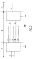
- Fig. 2 shows another embodiment of delay coding according to the invention, in which embodiment an AND gate 200 is implemented.
- the delay encoder 120 and the delay decoder 140 are standard electronic components utilized to make the conversion between the boolean domain I and the delay coding domain II and vice versa.
- variables X and Y are delay coded as described in Fig. 1 .
- the signal propagating on signal path ⁇ is a reference transition synchronized with the fastest signal propagating on either of the signal paths X0, X1, Y0 and Y1.
- Three possible scenarios can occur:
- circuit in Fig. 2 implements an AND gate 200.
- the verb 'to accelerate' is used to indicate the difference between a signal propagation speed on a wire caused by advantageous signal propagations on neighboring wires, and a signal propagation speed on a wire having no advantageous signal propagations on its neighboring wires, leaving the signal propagation on the wire to be more hampered by cross-talk with its environment. Consequently, the signal propagation speed in the first situation is better than the signal propagation speed in the second situation, hence the signal propagation on the wire in the first situation is 'accelerated' with respect to the signal propagation of the wire in the second situation. It is stipulated that the use of the verb 'to accelerate' as used in the aforementioned context should not necessarily be explained as an indication of an increase of the actual speed of a signal propagation on the wire.
- Fig. 4 shows a speed-matching gate 500 employed in the present invention.
- An important factor in interference delay logic is that signals such as the reference have the proper speed, i.e., a well-defined speed. A signal propagating over a wire in a random environment will always exhibit some delay resulting from the interaction of the wire with the environment.
- a wire from an interacting wire pair employing the techniques of the present invention may have a smaller delay than the delay from a random environment, because the cross-talk with the neighboring wire in the wire pair may be reduced due to the fact that both wires may carry matching transient signals.
- Drivers 502 are included in both output terminals 520 and 530 to reduce the load on the wire X1, in order to allow for an optimization of the propagation speed of the signal. Because the switching behavior on output terminal 530 matches the switching behavior on output terminal 520, the cross-talk between the output terminal 520 and its environment is reduced, thus reducing the effects of cross-talk on the output terminal 520, which improves the propagation speed of the signal on output terminal 520.
- Drivers 502 and receiver 504 may be implemented by any buffer or driver known from the art.
- transistors are only needed in the form of delay encoders 120 and delay decoders 140 when conversion is to be done between the boolean domain I, where signal values are represented by logic levels, and the delay coding domain II where signal values are represented by the difference in arrival time of signals.
- the relative number of transistors used in a logical network decreases as the number of cascaded gates increases, since all logical computations can be performed in the delay coding domain II and transistors are necessary only at the interfaces between the two domains I and II.
- An extensive network of delay coded gates would still only need transistors at the interfaces. Possibly, simple transistor buffers, e.g.
- drivers 502 are used to amplify the signals propagating on the signal paths, i.e., output terminals 520 and 530.
- the two wires each have an own driver 502 in order for acceleration to take place. Note that the length of the two wires is a design parameter; the longer the parallel run length of the two wires, the more acceleration is obtained.
- Delay coding can preferably be used in interconnections for electrical signals.
- Interconnections e.g., busses on a printed circuit board, are passive components for transmissions of bits from one place to another.
- Fig. 5 shows a typical bus structure 600 containing flip-flops 1, buffers 2 and wires 3 for amplification of signals propagating on the wires.
- delay coding By using delay coding, logical computations can be performed on the busses while transmitting the signals.
- Fig. 6 shows a circuit 700 implementing an embodiment of delay coding according to the invention when used on a bus structure or another multiple-wire arrangement.
- a data wire 610 is split into a program wire 620 and a signal wire 630.
- computation can only be performed when a transition takes place on the data wire 610.
- the signal wire 630 and the program wire 620 must be electrically coupled to each other in order to employ the effects of cross-talk, i.e., modifying the speed of the signal propagating on the signal wire 630. Synchronization of the program wire 620 and the signal wire 630 is an important issue, since the delay modification caused by the program wire 620 on the signal wire 630 should preferably be maximised.
- a standard delay decoder 140 can be used to convert delay coded signals to binary signals by comparing the transient behavior on signal wire 630 with that of reference wire 640.
- the wires 610, 620, 630, 640 may be equipped with appropriate driver circuits 602 to obtain the desired signal strength on the wires.
- Fig. 7 shows another embodiment of delay coding according to the invention when used on bus structures or other multiple-wire arrangements.
- the circuit 700 in Fig. 6 is represented by a block followed by a repeater 720.
- the block 700 and the repeater 720 forms a stage. Each stage can perform computing and employ data from the previous stages.
- the conventional transmission path for busses includes the signals propagating via "Data" and "Z”.
- Variables a, b, and c represent additional data transportation and Z-EXTRA represents additional computed data transportation. Note that data transport may take place without the performance of computation.
Landscapes
- Engineering & Computer Science (AREA)
- General Engineering & Computer Science (AREA)
- Physics & Mathematics (AREA)
- General Physics & Mathematics (AREA)
- Power Engineering (AREA)
- Computer Networks & Wireless Communication (AREA)
- Signal Processing (AREA)
- Theoretical Computer Science (AREA)
- Design And Manufacture Of Integrated Circuits (AREA)
- Compression, Expansion, Code Conversion, And Decoders (AREA)
- Pulse Circuits (AREA)
- Tests Of Electronic Circuits (AREA)
Abstract
Description
- The present invention relates to a method for coding information in an electronic circuit and an electronic circuit for coding information, said circuit comprising at least two electrically coupled signal paths.
- A well-known electrical phenomenon known as cross-talk exists among signal paths that are electrically coupled to each other. Cross-talk manifests itself by inducing voltage glitches on electrically coupled signal paths, which is seen as an undesired disturbance that has to be minimized. Cross-talk also manifests itself by modifying the speed of the signals travelling on these signal paths. Normally, neighboring signal paths will affect each other to a greater extent than paths located some distance away from each other, since the closer they are located to each other, the stronger the electrical coupling will be.
- For instance, consider two electrically coupled signal paths in an IC. This is normally the case when two parallel extending signal paths are located closely together. If a signal transition occurs on a signal path, it will propagate along the path with a given speed, reaching the end of the path within a given delay time. If, on the other hand, a signal transition occurs on both paths and the transition on each path is in the same direction, both transitions will propagate at a higher speed. The transitions will therefore reach the end of the path with a shorter delay. Cross-talk is thus effectively modulating the delay of signals propagating along signal paths being electrically coupled to each other. These effects are in the prior art usually seen as problems that have to be minimized or eliminated.
- For example,
GB 2,089,122 - It is a drawback that dedicated hardware has to be added to the integrated circuit for the sole purpose of eliminating cross-talk, especially when taking into consideration that the ongoing increase in integration density on ICs will lead to more pronounced occurrences of cross-talk, and a further increase in the required additional hardware, which has negative implications for the silicon real estate of the IC.
- Amongst others, it is an object of the present invention to provide an improved method and electronic circuit for coding information.
- This object is achieved by the invention in a first aspect in the form of a method for coding information in an electronic circuit, said circuit comprising at least two electrically coupled signal paths according to
claim 1 and in a second aspect in the form of an electronic circuit for coding information, said circuit comprising at least two electrically coupled signal paths according to claim 5. This has the advantage that cross-talk related additional hardware is utilized to generate useful information rather than to merely eliminate or reduce an effect that will become more and more pronounced with increasing integration densities on ICs. So, in accordance with the invention, cross-talk is being utilized rather than being countered. - At this point, it is stated that it is known per se to define a logic value by means of a delay between signal transitions on different signal paths. For instance, in 'A CMOS 160 Mb/s Phase Modulation I/O Interface Circuit' by Nogami et al. in Proc. Solid-State Circuits Conference 1994, 16 February 1994 pages 108-109, a phase modulation technique to define multi-bit values on a single conductor is disclosed. The various multi-bit values are defined by different delays between the rising edge of a signal transition of said conductor and the rising edge of a clock pulse on a different conductor. A similar technique is disclosed in European patent application
EP 1286470 , which has been filed before the priority date of the present application and has been published after this date, which is therefore only relevant to assessing the novelty of the present application. However, none of these documents disclose the utilization of cross-talk to manipulate the relative delay between the signal transitions. - According to the first aspect of the invention, a method for coding information is provided wherein the relative delay between signals propagating on at least two electrically coupled paths is determined when the signals make a transition from a first logic level to a second logic level. An output signal is then produced having a further logic level depending on the relative delay between the signals.
- According to the second aspect of the invention, an electronic circuit for coding information is provided comprising means arranged to determine the relative delay between signals propagating on at least two electrically coupled paths when the signals make a transition from a first logic level to a second logic level. The electronic circuit further comprises means arranged to produce an output signal having a further logic level depending on the relative delay between the signals.
- The invention is based on the idea that cross-talk between two electrically coupled signal paths can be utilized to perform a logical computation. A signal is propagating on two signal paths in the form of either rising or falling transitions. The relative delay between the transitions on the two paths determines the further logic value i.e., a logic "0" or a logic "1", of the output signal to be produced. This is hereinafter referred to as "delay coding". If the signal on the first path propagates faster than the signal on the second path, an output signal of a first further logic value is produced. If the signal on the second path propagates faster than the signal on the first path, an output signal of a second further logic value is produced.
- By employing the concept of delay coding, it is possible to implement logic gates performing computation by means of cross-talk, which is used to modify the speed of transitions propagating on electrically coupled signal paths and thus modulating delays. This is advantageous since logic gates comprised of transistors can be replaced by logic gates comprised of electrically coupled signal paths. Transistors are only needed when conversion is to be done between the boolean domain, where signal values are represented by logic levels, and the delay domain where signal values are represented by the difference in arrival time of signals.
- According to an embodiment of the invention, a logical signal is divided into two delay coded signals propagating on respective electrically coupled signal paths. A relative delay between the two delay coded signals is created by means of a delay encoder, e.g. a programmable delay circuit, a buffer or some other type of circuit having an inherent delay. Thereby, the conversion between the boolean domain, i.e., the standard digital binary domain, and the delay coding domain is performed. Standard delay decoders, for example metastability filters, can be used to convert delay coded signals to binary signals.
- The present invention will be described in greater detail with reference made to the accompanying drawings, in which:
-
Fig. 1 shows an embodiment of delay coding according to the invention; -
Fig. 2 shows another embodiment of delay coding according to the invention, in which embodiment an AND gate is implemented; -
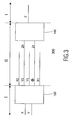
Fig. 3 shows another embodiment of delay coding according to the invention, in which embodiment an OR gate is implemented; -
Fig. 4 shows a speed-matching gate employed in the present invention; -
Fig. 5 shows a typical bus structure in which the present invention advantageously can be employed; -
Fig. 6 shows an embodiment of delay coding according to the invention when used on a bus structure; and -
Fig. 7 shows another embodiment of delay coding according to the invention when used on bus structures; -
Fig. 1 shows an embodiment of delay coding according to the invention. In delay coding two signal paths X0, X1 are needed for each binary variable X. The signal paths X0, X1 are constituted of for example wires, copper lines on a printed circuit board, signal lines in an integrated circuit etc. In order for cross-talk to emerge, electrical coupling between the signal paths X0, X1 must exist, which usually is the case among neighboring signal paths X0, X1. A signal is propagating on both signal paths X0, X1 in the form of either rising or falling transitions. The relative delay Δ between the transitions on the two paths X0, X1, i.e, when the signals make a transition from a first logic level to a second logic level, e.g., a "0"→ "1" transition or a "1→ "0" transition, determines the logic value of the output signal X to be produced. If the signal propagating on path X0 propagates faster than the signal on path X1, X has the logical value "0". If the signal propagating on path X0 propagates slower than the signal on path X1, X has the logical value "1". The delay coding scheme is the same for falling transitions. The further logic value, i.e., a logic "1" or "0", that is assigned to the output depending on the relative delay between the signals, i.e., depending on which of the signals propagates faster, is a mere matter of choice, i.e., convention. However, hereinafter the conventional delay coding scheme shown inFig. 1 will be used. -
Fig. 2 shows another embodiment of delay coding according to the invention, in which embodiment anAND gate 200 is implemented. As mentioned earlier, thedelay encoder 120 and thedelay decoder 140 are standard electronic components utilized to make the conversion between the boolean domain I and the delay coding domain II and vice versa. Assume that variables X and Y are delay coded as described inFig. 1 . The signal propagating on signal path Φ is a reference transition synchronized with the fastest signal propagating on either of the signal paths X0, X1, Y0 and Y1. Three possible scenarios can occur: - 1. Signals X and Y are both equal to logic "1". In this case the transitions on X1 and Y1 are faster than the transitions on X0 and Y0 in accordance with
Fig. 1 and synchronized with the reference. - 2. Signals X and Y are both equal to logic "0". In this case the transitions on X0 and Y0 are faster than the transitions on X1 and Y1 in accordance with
Fig. 1 and synchronized with the reference. - 3. The logical value on signals X and Y differ. In this case either the transitions on X0 and Y1 or the transitions on X1 and Y0 are faster in accordance with
Fig. 1 and either the transitions on X0 or Y0 are synchronized with the reference. - In
case 1, the signals propagating on X0 and Y0 do not influence the neighboring reference since they are slower than the reference while Y1 is accelerated by X1. Consequently, the transition on Z1 is faster than the transition on Z0 and thus, in accordance withFig. 1 , Z is equal to logic "1". - In
case 2, the signals on X0, X1, Y0 and Y1 are all accelerated. However, the signals propagating on X0 and Y0 now accelerate the neighboring reference. Consequently, the transition on Z0 is faster than the transition on Z1 and thus, in accordance withFig. 1 , Z is equal to logic "0". - In
case 3, either the signals propagating on X0 or Y0 are synchronized with the neighboring reference and, as a consequence, are able to accelerate the reference. As the signal on Y1 is not accelerated, the transition on Z0 is faster than the one on Z1. Consequently, in accordance withFig. 1 , Z is equal to logic "0". - Hence, studying these three cases, it can be seen that the circuit in
Fig. 2 implements an ANDgate 200. - By applying a similar reasoning, the function of an
OR gate 300 as shown inFig. 3 can be verified. - It will be understood by those skilled in the art that in the context of the present invention, the verb 'to accelerate' is used to indicate the difference between a signal propagation speed on a wire caused by advantageous signal propagations on neighboring wires, and a signal propagation speed on a wire having no advantageous signal propagations on its neighboring wires, leaving the signal propagation on the wire to be more hampered by cross-talk with its environment. Consequently, the signal propagation speed in the first situation is better than the signal propagation speed in the second situation, hence the signal propagation on the wire in the first situation is 'accelerated' with respect to the signal propagation of the wire in the second situation. It is stipulated that the use of the verb 'to accelerate' as used in the aforementioned context should not necessarily be explained as an indication of an increase of the actual speed of a signal propagation on the wire.
-
Fig. 4 shows a speed-matchinggate 500 employed in the present invention. An important factor in interference delay logic is that signals such as the reference have the proper speed, i.e., a well-defined speed. A signal propagating over a wire in a random environment will always exhibit some delay resulting from the interaction of the wire with the environment. In contrast, a wire from an interacting wire pair employing the techniques of the present invention may have a smaller delay than the delay from a random environment, because the cross-talk with the neighboring wire in the wire pair may be reduced due to the fact that both wires may carry matching transient signals. Consequently, in an arrangement where a substantial number of gates according to the invention are cascaded, signals propagating through these gates may substantially benefit from this effect, and properly accelerated references, i.e., references that exhibit optimized signal propagation speeds resulting from advantageous signal propagations on interacting wires, which match this benificial effect must be provided to ensure that the reference still defines the upper limit of the signal propagation speed. Speed-matching gates are thus required. An example of such a gate is illustrated inFig. 4 . The speed-matchinggate 500 has two output terminals, i.e.,output terminals open output terminal 530 tooutput terminal 520, the later being coupled to areceiver 504.Drivers 502 are included in bothoutput terminals output terminal 530 matches the switching behavior onoutput terminal 520, the cross-talk between theoutput terminal 520 and its environment is reduced, thus reducing the effects of cross-talk on theoutput terminal 520, which improves the propagation speed of the signal onoutput terminal 520.Drivers 502 andreceiver 504 may be implemented by any buffer or driver known from the art. - As previously mentioned, transistors are only needed in the form of
delay encoders 120 and delaydecoders 140 when conversion is to be done between the boolean domain I, where signal values are represented by logic levels, and the delay coding domain II where signal values are represented by the difference in arrival time of signals. The relative number of transistors used in a logical network decreases as the number of cascaded gates increases, since all logical computations can be performed in the delay coding domain II and transistors are necessary only at the interfaces between the two domains I and II. An extensive network of delay coded gates would still only need transistors at the interfaces. Possibly, simple transistor buffers, e.g.drivers 502, are used to amplify the signals propagating on the signal paths, i.e.,output terminals own driver 502 in order for acceleration to take place. Note that the length of the two wires is a design parameter; the longer the parallel run length of the two wires, the more acceleration is obtained. - Delay coding according to the invention can preferably be used in interconnections for electrical signals. Interconnections, e.g., busses on a printed circuit board, are passive components for transmissions of bits from one place to another.
Fig. 5 shows atypical bus structure 600 containing flip-flops 1,buffers 2 andwires 3 for amplification of signals propagating on the wires. By using delay coding, logical computations can be performed on the busses while transmitting the signals. -
Fig. 6 shows acircuit 700 implementing an embodiment of delay coding according to the invention when used on a bus structure or another multiple-wire arrangement. Adata wire 610 is split into aprogram wire 620 and asignal wire 630. As described earlier, computation can only be performed when a transition takes place on thedata wire 610. Thesignal wire 630 and theprogram wire 620 must be electrically coupled to each other in order to employ the effects of cross-talk, i.e., modifying the speed of the signal propagating on thesignal wire 630. Synchronization of theprogram wire 620 and thesignal wire 630 is an important issue, since the delay modification caused by theprogram wire 620 on thesignal wire 630 should preferably be maximised. As described earlier, astandard delay decoder 140 can be used to convert delay coded signals to binary signals by comparing the transient behavior onsignal wire 630 with that ofreference wire 640. Thewires appropriate driver circuits 602 to obtain the desired signal strength on the wires. - The principle of the logic computation will be described in the following. By default, the signal propagating on the reference wire 640 (which can be shared with other signal wires) is faster than the signal propagating on the
signal wire 630. This produces a logic value of "0" on the Z_EXTRA output ofdelay decoder 140. However, if the computation conditions are met, i.e. a*(b+c), the signal propagating on the signal wire will be accelerated by the signal propagating on theprogram wire 620. Hence, Z_EXTRA will be equal to logic "1" and the logical function Z_EXTRA = a*(b+c) has been implemented. By swapping the inputs X and Y of thedelay decoder 140, the inverse function is implemented. It should be clear that this particular logic function merely is exemplifying, and any logic function can be implemented. As can be seen inFig. 6 , thedelay encoder 120 is, as mentioned previously, implemented by means oftransistors -
Fig. 7 shows another embodiment of delay coding according to the invention when used on bus structures or other multiple-wire arrangements. Here, thecircuit 700 inFig. 6 is represented by a block followed by arepeater 720. Theblock 700 and therepeater 720 forms a stage. Each stage can perform computing and employ data from the previous stages. The conventional transmission path for busses includes the signals propagating via "Data" and "Z". Variables a, b, and c represent additional data transportation and Z-EXTRA represents additional computed data transportation. Note that data transport may take place without the performance of computation. - When cascading the stages as in
Fig. 7 , conversion is made from the boolean domain I to the delay coding domain II for each stage. When passing the data on to next stage, conversion is made from the delay coding domain II to the boolean domain I. - It should be noted that the above-mentioned embodiments illustrate rather than limit the invention, and that those skilled in the art will be able to design many alternative embodiments without departing from the scope of the appended claims. In the claims, any reference signs placed between parentheses shall not be construed as limiting the claim. The word "comprising" does not exclude the presence of elements or steps other than those listed in a claim. The word "a" or "an" preceding an element does not exclude the presence of a plurality of such elements. In the device claim enumerating several means, several of these means can be embodied by one and the same item of hardware. The mere fact that certain measures are recited in mutually different dependent claims does not indicate that a combination of these measures cannot be used to advantage.
Claims (7)
- A method for coding information in an electronic circuit (700), said circuit comprising at least two electrically coupled signal paths (620; 630), the method comprising the steps of:determining a relative delay between signals propagating on said paths (620; 630) when said signals make a transition from a first logic level to a second logic level; andproducing an output signal (Z_EXTRA) having a further logic level depending on the relative delay between said signals;characterized by manipulating the relative delay by modifying the propagation speed of one of said signals.
- The method according to claim 1, further comprising the step of:dividing a logical signal (X, Y) into two signals (X0; X1, Y0; Y1) to be propagated on a respective one of said signal paths (620; 630).
- The method according to claim 1 or 2, wherein the step of manipulating the relative delay comprises creating a reference signal (Φ) being synchronized with the fastest signal propagating on either of said signal paths (620; 630).
- The method according to claim 1, wherein the producing step is performed by means of a delay decoder (140).
- An electronic circuit (700) for coding information, comprising:at least two electrically coupled signal paths (620; 630);means (640) for determining a relative delay between signals propagating on said paths (620; 630) when said signals make a transition from a first logic level to a second logic level;means (140) for producing an output signal (Z _EXTRA) having a further logic level depending on the relative delay between said two signals;characterized by further comprising means for creating a reference signal (Φ) being synchronized with the fastest signal propagating on either of said signal paths (620; 630) for modifying the propagation speed of one of said signals.
- The circuit according to claim 5, further comprising:means for dividing a logical signal (X, Y) into two signals (X0; X1, Y0; Y1) to be propagated on a respective one of said signal paths (620; 630).
- The circuit according to claim 5, wherein the producing means (140) comprise a delay decoder.
Priority Applications (1)
| Application Number | Priority Date | Filing Date | Title |
|---|---|---|---|
| EP03795107A EP1540828B1 (en) | 2002-09-13 | 2003-08-06 | Coding of information in integrated circuits |
Applications Claiming Priority (4)
| Application Number | Priority Date | Filing Date | Title |
|---|---|---|---|
| EP02078779 | 2002-09-13 | ||
| EP02078779 | 2002-09-13 | ||
| PCT/IB2003/003496 WO2004025838A1 (en) | 2002-09-13 | 2003-08-06 | Coding of information in integrated circuits |
| EP03795107A EP1540828B1 (en) | 2002-09-13 | 2003-08-06 | Coding of information in integrated circuits |
Publications (2)
| Publication Number | Publication Date |
|---|---|
| EP1540828A1 EP1540828A1 (en) | 2005-06-15 |
| EP1540828B1 true EP1540828B1 (en) | 2009-02-25 |
Family
ID=31985093
Family Applications (1)
| Application Number | Title | Priority Date | Filing Date |
|---|---|---|---|
| EP03795107A Expired - Lifetime EP1540828B1 (en) | 2002-09-13 | 2003-08-06 | Coding of information in integrated circuits |
Country Status (10)
| Country | Link |
|---|---|
| US (1) | US7515074B2 (en) |
| EP (1) | EP1540828B1 (en) |
| JP (1) | JP2005538632A (en) |
| KR (1) | KR20050043945A (en) |
| CN (1) | CN100481731C (en) |
| AT (1) | ATE424060T1 (en) |
| AU (1) | AU2003255884A1 (en) |
| DE (1) | DE60326363D1 (en) |
| TW (1) | TWI310594B (en) |
| WO (1) | WO2004025838A1 (en) |
Families Citing this family (1)
| Publication number | Priority date | Publication date | Assignee | Title |
|---|---|---|---|---|
| US8145442B2 (en) * | 2009-01-30 | 2012-03-27 | Synopsys, Inc. | Fast and accurate estimation of gate output loading |
Citations (1)
| Publication number | Priority date | Publication date | Assignee | Title |
|---|---|---|---|---|
| EP1286470A2 (en) * | 2001-07-19 | 2003-02-26 | Fujitsu Limited | Input/output interface and semiconductor integrated circuit having input/output interface |
Family Cites Families (19)
| Publication number | Priority date | Publication date | Assignee | Title |
|---|---|---|---|---|
| US3084223A (en) * | 1960-12-23 | 1963-04-02 | Bell Telephone Labor Inc | Crosstalk reduction in plural carrier multiplex systems |
| JPS5140449A (en) * | 1974-10-04 | 1976-04-05 | Toray Industries | MAKITORISOCHI |
| JPS5784149A (en) * | 1980-11-14 | 1982-05-26 | Hitachi Ltd | Semiconductor integrated circuit device |
| JPS604347A (en) * | 1983-06-22 | 1985-01-10 | Fuji Xerox Co Ltd | System for coping with trouble in digital signal transmission system |
| US5493588A (en) * | 1992-01-22 | 1996-02-20 | Trimble Navigation Limited | Multipath compensation for code phase signals |
| JP3136742B2 (en) * | 1992-02-14 | 2001-02-19 | 日産自動車株式会社 | Communication device |
| IL120538A (en) * | 1997-03-26 | 2000-11-21 | Dspc Tech Ltd | Method and apparatus for reducing spread-spectrum noise |
| US6148038A (en) * | 1997-03-31 | 2000-11-14 | Sun Microsystems, Inc. | Circuit for detecting and decoding phase encoded digital serial data |
| US6480548B1 (en) * | 1997-11-17 | 2002-11-12 | Silicon Graphics, Inc. | Spacial derivative bus encoder and decoder |
| AU769804B2 (en) * | 1998-03-11 | 2004-02-05 | Thomson Licensing S.A. | Digital signal modulation system |
| JP3137328B2 (en) * | 1998-04-22 | 2001-02-19 | 富士通株式会社 | Noise removal method and transmission circuit |
| US6731622B1 (en) * | 1998-05-01 | 2004-05-04 | Telefonaktiebolaget Lm Ericsson (Publ) | Multipath propagation delay determining means using periodically inserted pilot symbols |
| JP2001326584A (en) * | 2000-05-18 | 2001-11-22 | Nec Corp | Path detection system and receiver |
| KR100335503B1 (en) * | 2000-06-26 | 2002-05-08 | 윤종용 | Signal transmission circuit, signal transmission method for synchronizing different delay characteristics, and data latch circuit of semiconductor device having the same |
| JP3813490B2 (en) * | 2001-10-30 | 2006-08-23 | 富士通株式会社 | Spread spectrum rake receiver |
| JP2003316736A (en) * | 2002-04-19 | 2003-11-07 | Oki Electric Ind Co Ltd | Usb circuit and data structure |
| US6958721B2 (en) * | 2003-09-18 | 2005-10-25 | The Regents Of The University Of Colorado | Matched delay line voltage converter |
| JP3927576B2 (en) * | 2005-01-31 | 2007-06-13 | 富士通株式会社 | Input/output interface and semiconductor integrated circuit |
| US20070271535A1 (en) * | 2006-05-16 | 2007-11-22 | National Tsing Hua University | Method for crosstalk elimination and bus architecture performing the same |
-
2003
- 2003-08-06 KR KR1020057004206A patent/KR20050043945A/en not_active Ceased
- 2003-08-06 EP EP03795107A patent/EP1540828B1/en not_active Expired - Lifetime
- 2003-08-06 DE DE60326363T patent/DE60326363D1/en not_active Expired - Lifetime
- 2003-08-06 WO PCT/IB2003/003496 patent/WO2004025838A1/en not_active Ceased
- 2003-08-06 US US10/527,551 patent/US7515074B2/en not_active Expired - Lifetime
- 2003-08-06 AT AT03795107T patent/ATE424060T1/en not_active IP Right Cessation
- 2003-08-06 AU AU2003255884A patent/AU2003255884A1/en not_active Abandoned
- 2003-08-06 CN CNB038217961A patent/CN100481731C/en not_active Expired - Fee Related
- 2003-08-06 JP JP2004535729A patent/JP2005538632A/en active Pending
- 2003-09-10 TW TW092125072A patent/TWI310594B/en not_active IP Right Cessation
Patent Citations (1)
| Publication number | Priority date | Publication date | Assignee | Title |
|---|---|---|---|---|
| EP1286470A2 (en) * | 2001-07-19 | 2003-02-26 | Fujitsu Limited | Input/output interface and semiconductor integrated circuit having input/output interface |
Also Published As
| Publication number | Publication date |
|---|---|
| ATE424060T1 (en) | 2009-03-15 |
| WO2004025838A1 (en) | 2004-03-25 |
| CN100481731C (en) | 2009-04-22 |
| US20050270194A1 (en) | 2005-12-08 |
| DE60326363D1 (en) | 2009-04-09 |
| EP1540828A1 (en) | 2005-06-15 |
| CN1682447A (en) | 2005-10-12 |
| KR20050043945A (en) | 2005-05-11 |
| JP2005538632A (en) | 2005-12-15 |
| US7515074B2 (en) | 2009-04-07 |
| TWI310594B (en) | 2009-06-01 |
| TW200419734A (en) | 2004-10-01 |
| AU2003255884A1 (en) | 2004-04-30 |
Similar Documents
| Publication | Publication Date | Title |
|---|---|---|
| JPH10293636A (en) | Interleaved inverters to reduce capacitive coupling in transmission lines | |
| US6711089B2 (en) | Method and apparatus for performing signal synchronization | |
| EP1540828B1 (en) | Coding of information in integrated circuits | |
| KR100209224B1 (en) | High speed multiplex | |
| KR100678332B1 (en) | Bus Driver with Data-Dependent Drive Strength Control Logic | |
| US6642748B2 (en) | Input circuit | |
| US6690221B1 (en) | Method and apparatus to delay signal latching | |
| KR20020017082A (en) | Memory module preventing skew of signal lines | |
| US7492205B2 (en) | Clock generator | |
| US6144224A (en) | Clock distribution network with dual wire routing | |
| JP3198999B2 (en) | Method of forming clock tree of scan path circuit | |
| JPH11340796A (en) | Flip-flop circuit | |
| AU720687B2 (en) | Logic circuits | |
| JPS62217632A (en) | Semiconductor integrated circuit | |
| KR0154723B1 (en) | Input circuit of clock signal | |
| KR0158640B1 (en) | Data bus control circuit | |
| JPH0675658A (en) | Semiconductor integrated circuit | |
| JPH08307460A (en) | Digital signal transmission line | |
| JPH01166968A (en) | Logic device | |
| JPH02285708A (en) | Flip-flop ic | |
| JPH11330374A (en) | Semiconductor integrated circuit device | |
| JPH09331260A (en) | Semiconductor device | |
| JPH04222995A (en) | Shift register circuit | |
| JPH0370414B2 (en) | ||
| JPH065705A (en) | Semiconductor integrated circuit |
Legal Events
| Date | Code | Title | Description |
|---|---|---|---|
| PUAI | Public reference made under article 153(3) epc to a published international application that has entered the european phase |
Free format text: ORIGINAL CODE: 0009012 |
|
| 17P | Request for examination filed |
Effective date: 20050413 |
|
| AK | Designated contracting states |
Kind code of ref document: A1 Designated state(s): AT BE BG CH CY CZ DE DK EE ES FI FR GB GR HU IE IT LI LU MC NL PT RO SE SI SK TR |
|
| AX | Request for extension of the european patent |
Extension state: AL LT LV MK |
|
| DAX | Request for extension of the european patent (deleted) | ||
| 17Q | First examination report despatched |
Effective date: 20060110 |
|
| RAP1 | Party data changed (applicant data changed or rights of an application transferred) |
Owner name: NXP B.V. |
|
| GRAP | Despatch of communication of intention to grant a patent |
Free format text: ORIGINAL CODE: EPIDOSNIGR1 |
|
| GRAS | Grant fee paid |
Free format text: ORIGINAL CODE: EPIDOSNIGR3 |
|
| GRAA | (expected) grant |
Free format text: ORIGINAL CODE: 0009210 |
|
| AK | Designated contracting states |
Kind code of ref document: B1 Designated state(s): AT BE BG CH CY CZ DE DK EE ES FI FR GB GR HU IE IT LI LU MC NL PT RO SE SI SK TR |
|
| REG | Reference to a national code |
Ref country code: GB Ref legal event code: FG4D |
|
| REG | Reference to a national code |
Ref country code: CH Ref legal event code: EP |
|
| REG | Reference to a national code |
Ref country code: IE Ref legal event code: FG4D |
|
| REF | Corresponds to: |
Ref document number: 60326363 Country of ref document: DE Date of ref document: 20090409 Kind code of ref document: P |
|
| PG25 | Lapsed in a contracting state [announced via postgrant information from national office to epo] |
Ref country code: FI Free format text: LAPSE BECAUSE OF FAILURE TO SUBMIT A TRANSLATION OF THE DESCRIPTION OR TO PAY THE FEE WITHIN THE PRESCRIBED TIME-LIMIT Effective date: 20090225 Ref country code: SI Free format text: LAPSE BECAUSE OF FAILURE TO SUBMIT A TRANSLATION OF THE DESCRIPTION OR TO PAY THE FEE WITHIN THE PRESCRIBED TIME-LIMIT Effective date: 20090225 Ref country code: NL Free format text: LAPSE BECAUSE OF FAILURE TO SUBMIT A TRANSLATION OF THE DESCRIPTION OR TO PAY THE FEE WITHIN THE PRESCRIBED TIME-LIMIT Effective date: 20090225 |
|
| NLV1 | Nl: lapsed or annulled due to failure to fulfill the requirements of art. 29p and 29m of the patents act | ||
| PG25 | Lapsed in a contracting state [announced via postgrant information from national office to epo] |
Ref country code: AT Free format text: LAPSE BECAUSE OF FAILURE TO SUBMIT A TRANSLATION OF THE DESCRIPTION OR TO PAY THE FEE WITHIN THE PRESCRIBED TIME-LIMIT Effective date: 20090225 Ref country code: SE Free format text: LAPSE BECAUSE OF FAILURE TO SUBMIT A TRANSLATION OF THE DESCRIPTION OR TO PAY THE FEE WITHIN THE PRESCRIBED TIME-LIMIT Effective date: 20090525 |
|
| PG25 | Lapsed in a contracting state [announced via postgrant information from national office to epo] |
Ref country code: BE Free format text: LAPSE BECAUSE OF FAILURE TO SUBMIT A TRANSLATION OF THE DESCRIPTION OR TO PAY THE FEE WITHIN THE PRESCRIBED TIME-LIMIT Effective date: 20090225 |
|
| PG25 | Lapsed in a contracting state [announced via postgrant information from national office to epo] |
Ref country code: ES Free format text: LAPSE BECAUSE OF FAILURE TO SUBMIT A TRANSLATION OF THE DESCRIPTION OR TO PAY THE FEE WITHIN THE PRESCRIBED TIME-LIMIT Effective date: 20090605 Ref country code: PT Free format text: LAPSE BECAUSE OF FAILURE TO SUBMIT A TRANSLATION OF THE DESCRIPTION OR TO PAY THE FEE WITHIN THE PRESCRIBED TIME-LIMIT Effective date: 20090812 Ref country code: CZ Free format text: LAPSE BECAUSE OF FAILURE TO SUBMIT A TRANSLATION OF THE DESCRIPTION OR TO PAY THE FEE WITHIN THE PRESCRIBED TIME-LIMIT Effective date: 20090225 Ref country code: DK Free format text: LAPSE BECAUSE OF FAILURE TO SUBMIT A TRANSLATION OF THE DESCRIPTION OR TO PAY THE FEE WITHIN THE PRESCRIBED TIME-LIMIT Effective date: 20090225 Ref country code: EE Free format text: LAPSE BECAUSE OF FAILURE TO SUBMIT A TRANSLATION OF THE DESCRIPTION OR TO PAY THE FEE WITHIN THE PRESCRIBED TIME-LIMIT Effective date: 20090225 |
|
| PG25 | Lapsed in a contracting state [announced via postgrant information from national office to epo] |
Ref country code: RO Free format text: LAPSE BECAUSE OF FAILURE TO SUBMIT A TRANSLATION OF THE DESCRIPTION OR TO PAY THE FEE WITHIN THE PRESCRIBED TIME-LIMIT Effective date: 20090225 Ref country code: SK Free format text: LAPSE BECAUSE OF FAILURE TO SUBMIT A TRANSLATION OF THE DESCRIPTION OR TO PAY THE FEE WITHIN THE PRESCRIBED TIME-LIMIT Effective date: 20090225 |
|
| PLBE | No opposition filed within time limit |
Free format text: ORIGINAL CODE: 0009261 |
|
| STAA | Information on the status of an ep patent application or granted ep patent |
Free format text: STATUS: NO OPPOSITION FILED WITHIN TIME LIMIT |
|
| PG25 | Lapsed in a contracting state [announced via postgrant information from national office to epo] |
Ref country code: BG Free format text: LAPSE BECAUSE OF FAILURE TO SUBMIT A TRANSLATION OF THE DESCRIPTION OR TO PAY THE FEE WITHIN THE PRESCRIBED TIME-LIMIT Effective date: 20090525 |
|
| 26N | No opposition filed |
Effective date: 20091126 |
|
| PG25 | Lapsed in a contracting state [announced via postgrant information from national office to epo] |
Ref country code: MC Free format text: LAPSE BECAUSE OF NON-PAYMENT OF DUE FEES Effective date: 20090831 |
|
| REG | Reference to a national code |
Ref country code: CH Ref legal event code: PL |
|
| PG25 | Lapsed in a contracting state [announced via postgrant information from national office to epo] |
Ref country code: LI Free format text: LAPSE BECAUSE OF NON-PAYMENT OF DUE FEES Effective date: 20090831 Ref country code: CH Free format text: LAPSE BECAUSE OF NON-PAYMENT OF DUE FEES Effective date: 20090831 |
|
| REG | Reference to a national code |
Ref country code: IE Ref legal event code: MM4A |
|
| PG25 | Lapsed in a contracting state [announced via postgrant information from national office to epo] |
Ref country code: IE Free format text: LAPSE BECAUSE OF NON-PAYMENT OF DUE FEES Effective date: 20090806 |
|
| PG25 | Lapsed in a contracting state [announced via postgrant information from national office to epo] |
Ref country code: GR Free format text: LAPSE BECAUSE OF FAILURE TO SUBMIT A TRANSLATION OF THE DESCRIPTION OR TO PAY THE FEE WITHIN THE PRESCRIBED TIME-LIMIT Effective date: 20090526 |
|
| PG25 | Lapsed in a contracting state [announced via postgrant information from national office to epo] |
Ref country code: IT Free format text: LAPSE BECAUSE OF FAILURE TO SUBMIT A TRANSLATION OF THE DESCRIPTION OR TO PAY THE FEE WITHIN THE PRESCRIBED TIME-LIMIT Effective date: 20090225 |
|
| PG25 | Lapsed in a contracting state [announced via postgrant information from national office to epo] |
Ref country code: LU Free format text: LAPSE BECAUSE OF NON-PAYMENT OF DUE FEES Effective date: 20090806 |
|
| PG25 | Lapsed in a contracting state [announced via postgrant information from national office to epo] |
Ref country code: HU Free format text: LAPSE BECAUSE OF FAILURE TO SUBMIT A TRANSLATION OF THE DESCRIPTION OR TO PAY THE FEE WITHIN THE PRESCRIBED TIME-LIMIT Effective date: 20090826 |
|
| PG25 | Lapsed in a contracting state [announced via postgrant information from national office to epo] |
Ref country code: TR Free format text: LAPSE BECAUSE OF FAILURE TO SUBMIT A TRANSLATION OF THE DESCRIPTION OR TO PAY THE FEE WITHIN THE PRESCRIBED TIME-LIMIT Effective date: 20090225 |
|
| PG25 | Lapsed in a contracting state [announced via postgrant information from national office to epo] |
Ref country code: CY Free format text: LAPSE BECAUSE OF FAILURE TO SUBMIT A TRANSLATION OF THE DESCRIPTION OR TO PAY THE FEE WITHIN THE PRESCRIBED TIME-LIMIT Effective date: 20090225 |
|
| PGFP | Annual fee paid to national office [announced via postgrant information from national office to epo] |
Ref country code: GB Payment date: 20120725 Year of fee payment: 10 |
|
| GBPC | Gb: european patent ceased through non-payment of renewal fee |
Effective date: 20130806 |
|
| PG25 | Lapsed in a contracting state [announced via postgrant information from national office to epo] |
Ref country code: GB Free format text: LAPSE BECAUSE OF NON-PAYMENT OF DUE FEES Effective date: 20130806 |
|
| REG | Reference to a national code |
Ref country code: FR Ref legal event code: PLFP Year of fee payment: 13 |
|
| REG | Reference to a national code |
Ref country code: DE Ref legal event code: R082 Ref document number: 60326363 Country of ref document: DE Representative=s name: MUELLER-BORE & PARTNER PATENTANWAELTE PARTG MB, DE Ref country code: DE Ref legal event code: R081 Ref document number: 60326363 Country of ref document: DE Owner name: LLL HOLDINGS 6, LLC, WILMINGTON, US Free format text: FORMER OWNER: NXP B.V., EINDHOVEN, NL Ref country code: DE Ref legal event code: R081 Ref document number: 60326363 Country of ref document: DE Owner name: III HOLDINGS 6, LLC, WILMINGTON, US Free format text: FORMER OWNER: NXP B.V., EINDHOVEN, NL |
|
| REG | Reference to a national code |
Ref country code: FR Ref legal event code: TP Owner name: III HOLDINGS 6, LLC, US Effective date: 20160118 |
|
| REG | Reference to a national code |
Ref country code: FR Ref legal event code: PLFP Year of fee payment: 14 |
|
| REG | Reference to a national code |
Ref country code: FR Ref legal event code: PLFP Year of fee payment: 15 |
|
| REG | Reference to a national code |
Ref country code: DE Ref legal event code: R082 Ref document number: 60326363 Country of ref document: DE Representative=s name: MUELLER-BORE & PARTNER PATENTANWAELTE PARTG MB, DE Ref country code: DE Ref legal event code: R081 Ref document number: 60326363 Country of ref document: DE Owner name: III HOLDINGS 6, LLC, WILMINGTON, US Free format text: FORMER OWNER: LLL HOLDINGS 6, LLC, WILMINGTON, DEL., US |
|
| PGFP | Annual fee paid to national office [announced via postgrant information from national office to epo] |
Ref country code: FR Payment date: 20170720 Year of fee payment: 15 Ref country code: DE Payment date: 20170825 Year of fee payment: 15 |
|
| REG | Reference to a national code |
Ref country code: DE Ref legal event code: R119 Ref document number: 60326363 Country of ref document: DE |
|
| PG25 | Lapsed in a contracting state [announced via postgrant information from national office to epo] |
Ref country code: DE Free format text: LAPSE BECAUSE OF NON-PAYMENT OF DUE FEES Effective date: 20190301 |
|
| PG25 | Lapsed in a contracting state [announced via postgrant information from national office to epo] |
Ref country code: FR Free format text: LAPSE BECAUSE OF NON-PAYMENT OF DUE FEES Effective date: 20180831 |