EP1533843A2 - Elektrolumineszente Vorrichtung mit niederohmigen Zuleitungen - Google Patents
Elektrolumineszente Vorrichtung mit niederohmigen Zuleitungen Download PDFInfo
- Publication number
- EP1533843A2 EP1533843A2 EP04090450A EP04090450A EP1533843A2 EP 1533843 A2 EP1533843 A2 EP 1533843A2 EP 04090450 A EP04090450 A EP 04090450A EP 04090450 A EP04090450 A EP 04090450A EP 1533843 A2 EP1533843 A2 EP 1533843A2
- Authority
- EP
- European Patent Office
- Prior art keywords
- lead
- width
- organic
- lead line
- lines
- Prior art date
- Legal status (The legal status is an assumption and is not a legal conclusion. Google has not performed a legal analysis and makes no representation as to the accuracy of the status listed.)
- Withdrawn
Links
Images



Classifications
-
- H—ELECTRICITY
- H10—SEMICONDUCTOR DEVICES; ELECTRIC SOLID-STATE DEVICES NOT OTHERWISE PROVIDED FOR
- H10K—ORGANIC ELECTRIC SOLID-STATE DEVICES
- H10K59/00—Integrated devices, or assemblies of multiple devices, comprising at least one organic light-emitting element covered by group H10K50/00
- H10K59/10—OLED displays
- H10K59/17—Passive-matrix OLED displays
- H10K59/179—Interconnections, e.g. wiring lines or terminals
-
- H—ELECTRICITY
- H05—ELECTRIC TECHNIQUES NOT OTHERWISE PROVIDED FOR
- H05B—ELECTRIC HEATING; ELECTRIC LIGHT SOURCES NOT OTHERWISE PROVIDED FOR; CIRCUIT ARRANGEMENTS FOR ELECTRIC LIGHT SOURCES, IN GENERAL
- H05B33/00—Electroluminescent light sources
- H05B33/12—Light sources with substantially two-dimensional [2D] radiating surfaces
- H05B33/26—Light sources with substantially two-dimensional [2D] radiating surfaces characterised by the composition or arrangement of the conductive material used as an electrode
-
- H—ELECTRICITY
- H10—SEMICONDUCTOR DEVICES; ELECTRIC SOLID-STATE DEVICES NOT OTHERWISE PROVIDED FOR
- H10K—ORGANIC ELECTRIC SOLID-STATE DEVICES
- H10K50/00—Organic light-emitting devices
- H10K50/80—Constructional details
- H10K50/84—Passivation; Containers; Encapsulations
- H10K50/841—Self-supporting sealing arrangements
-
- H—ELECTRICITY
- H10—SEMICONDUCTOR DEVICES; ELECTRIC SOLID-STATE DEVICES NOT OTHERWISE PROVIDED FOR
- H10K—ORGANIC ELECTRIC SOLID-STATE DEVICES
- H10K50/00—Organic light-emitting devices
- H10K50/80—Constructional details
- H10K50/84—Passivation; Containers; Encapsulations
- H10K50/846—Passivation; Containers; Encapsulations comprising getter material or desiccants
-
- H—ELECTRICITY
- H10—SEMICONDUCTOR DEVICES; ELECTRIC SOLID-STATE DEVICES NOT OTHERWISE PROVIDED FOR
- H10K—ORGANIC ELECTRIC SOLID-STATE DEVICES
- H10K59/00—Integrated devices, or assemblies of multiple devices, comprising at least one organic light-emitting element covered by group H10K50/00
- H10K59/80—Constructional details
- H10K59/87—Passivation; Containers; Encapsulations
- H10K59/871—Self-supporting sealing arrangements
Definitions
- the present invention relates to an electroluminescence device, and more particularly, to an electroluminescence device having lead lines that are connected to a plurality of electrodes forming an electroluminescence unit, the lead lines having different widths corresponding to lengths thereof.
- Flat panel displays are replacing the conventional cathode ray tube (CRT) devices.
- CRT cathode ray tube
- Flat panel displays are either emissive type or non-emissive type depending upon how the panel emits light.
- a flat CRT, a plasma display panel device, a vacuum fluorescent display device, a field emission display device, and an electroluminescence (EL) display device are emissive type display device.
- a liquid crystal display device is a non-emissive type display device.
- An organic EL display device is an emissive type display device that uses a phenomenon in which positive electrodes and negative electrodes inject electrons and holes, into an organic thin film, that combine to form exitons, which generate light of a certain wavelength.
- the organic EL display device may be driven with a low voltage, formed in a thin plate type with light weight, has a wide viewing angle and a fast response speed.
- An organic EL device may include positive electrodes, an organic layer, and negative electrodes that are stacked on a substrate.
- the substrate is typically formed using a glass, however, in some cases, a bendable plastic or a bendable film may be used.
- Indium tin oxide (ITO) may be used as the positive electrode, which may be formed through a vacuum deposition method or a sputtering method.
- Magnesium (Mg), lithium (Li), and other similar substances that have a low work function may be used as the negative electrode.
- the organic layer may be formed using various organic materials, and it may be doped by fluorescence dye or phosphorescence dye to improve its light emitting efficiency.
- the organic layer may include an organic emitting layer (EML), where the holes and electrons combine to form exitons and emit light. In order to improve the light emitting efficiency, the holes and electrons should be smoothly transported to the organic EML.
- EML organic emitting layer
- an electron transport layer (ETL) may be disposed between the negative electrode and the organic EML
- a hole transport layer (HTL) may be disposed between the positive electrode and the organic EML.
- HIL hole injection layer
- EIL electron injection layer
- the ITO electrode may be formed on a glass substrate by a sputtering process
- the organic EML and the metal electrodes may be formed in an evaporation method in a vacuum using a deposition apparatus including a chamber, a material evaporation source, a thickness monitor, and a metal mask.
- a desiccant is then injected into the organic OL device, and the device is sealed under a vacuum or nitrogen atmosphere, thereby increasing its durability, which is adversely affected by moisture and oxygen.
- FIG. 1A is an exploded perspective view showing a configuration of a conventional organic EL device.
- the organic EL device includes a substrate 10, and an active area 20 that is formed on a surface of the substrate 10 to form images.
- a cap 12 is bonded with the substrate to cover and seal the active area 20, and an electrode terminal portion 30, for supplying electric current to the active area 20, extends to the outer portion of the cap 12.
- a flexible printed circuit board (PCB) 13 is joined on the terminal unit 30, at a portion not covered by the cap 12, and is coupled to a circuit portion (not shown) for driving the active area 20.
- the electrode terminal portion 30 includes a first electrode terminal unit 31 and a second electrode terminal unit 32.
- the active area 20 includes stripe-shaped first electrode lines 21 that are connected to the first electrode terminal unit 31 and spaced at predetermined intervals as positive electrodes.
- Organic layers 24 are deposited on the first electrode lines 21 in predetermined patterns, and second electrode lines 22, insulated from the first electrode lines 21, are electrically coupled to the second electrode terminal unit 32, and formed on an upper portion of the organic layers 24 as negative electrodes.
- the active area 20 includes an insulating layer 23 that prevents the first electrode lines 21 and the second electrode lines 23 from short circuiting.
- the organic EL device is a current driving device, its light emitting efficiency is closely related to the first and second electrode lines on the active area and the resistance of the lines out of the active area. If the active area electrode lines have a high resistance, this may cause a voltage drop that generates a brightness difference between the pixels, thereby lowering image quality. Thus, many methods for reducing the electrode line resistance on the active area have been suggested.
- Japanese Laid-open Patent No. 2002-8871 discloses a conductive thick portion that is thicker than the active area electrode lines in order to reduce the resistance of the lead lines besides the first electrode lines and the second electrode lines on the active area. Generally, as shown in FIG.
- the following equation may be used to determine the resistance of a lead line on a terminal portion having a width (w), a thickness (xj), and a length (L).
- ⁇ denotes a specific resistance
- x j denotes a thickness of the lead line
- w denotes a width of the lead line
- R s denotes a sheet resistance.
- the resistance may be reduced by additionally forming the conductive thick portion with respect to the lead lines.
- the thickness of the lead line may need to be increased significantly in order to satisfy the required degree of resistance decrease.
- a plurality of lead lines will typically have the same width and length. But when the lead lines of the terminal portion are disposed densely to improve substrate mounting convenience and the convenience of arranging other elements on the substrate, the lengths of the lead lines will differ, therefore, resistances will differ. As lead line length increases, the resistance difference and the voltage drop also increase. Therefore, the organic EL device's driving voltage and power consumption increase.
- the present invention provides an organic electroluminescence (EL) device including a plurality of lines having widths corresponding to lengths thereof so that the different length lead lines may have uniform resistance.
- EL organic electroluminescence
- the present invention discloses an organic EL device including a plurality of electrodes formed on a substrate, and a plurality of lead lines are coupled to the plurality of electrodes. At least two or more lead lines among the plurality of lead lines have different widths, and a longer lead line among the plural lead lines has a larger width than a width of a shorter lead line.
- the present invention also discloses a flat panel display device including a substrate, on which a plurality of electrodes are disposed, and a plurality of lead lines coupled to the plurality of electrodes. At least two or more lead lines among the plurality of lead lines have different widths, and a width of a longer lead line is greater than a width of a shorter lead line.
- FIG. 1A is an exploded perspective view of a conventional organic electroluminescence (EL) device.
- EL organic electroluminescence
- FIG. 1B shows a conductive element having a predetermined size.
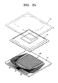
- FIG. 2A is an exploded perspective view of an organic EL device according to an exemplary embodiment of the present invention.
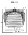
- FIG. 2B is a plan view of an enlarged part of the organic EL device of FIG. 2A.
- FIG. 3 is a cross-sectional view taken along line A-A of FIG. 2B.
- FIG. 2A is an exploded perspective view of a organic electroluminescence (EL) device according to an exemplary embodiment of the present invention
- FIG. 2B is a plan view showing an enlarged part of the organic EL device of FIG. 2A.
- an organic EL device of this exemplary embodiment of the present invention includes a substrate 10, on which a plurality of electrodes (or electrode lines) forming an active area 20 are disposed.
- a cap 12 contains a desiccant and is sealed with the substrate 10 to prevent the active area 20 from being infiltrated by moisture, and a flexible printed circuit board (PCB) 13 connects the organic EL device to a circuit driving unit (not shown).
- the cap and substrate may be joined at area 40.
- a plurality of electrode lines include a plurality of first electrode lines 21 as positive electrodes and a plurality of second electrode lines 22 as negative electrodes.
- the first electrode lines 21 are connected to first lead lines 31 having a first terminal unit 41
- the second electrode lines 22 are connected to second lead lines 32 having a second terminal unit 42.
- the second lead lines 32 may be manufactured to include an indium tin oxide (ITO) portion 32a and a metal or alloy portion 32b.
- Lead lines 31 may be similarly manufactured.
- the metal or alloy portion 32b may be formed of metal or alloy having low resistance, such as Cr, Al, Ag, Au, Pt, Pd, Ni, Mo, Ta, Ti, W, C, Fe, In, Ag-Mg, Zn, or other like substances.
- first lead lines 31 and the second lead lines 32 may be lead lines of 1-pad type. As shown in FIG. 2A and FIG. 2B, they may also be formed on a single side of the substrate. In order to minimize lead line resistance, first lead lines 31 and second lead lines 32 have minimum lengths and different widths. Specifically, in order to compensate for the resistance difference caused by different lead line lengths, a longer lead line may have a wider width at its terminal unit portion than that of a shorter lead line. The lengths of the first and second lead lines 31 and 32 may be controlled by passing the lead lines through appropriate positions.
- the ratio of the length of a first lead line 31 to the width of its first terminal unit 41 may be the same for the first lead lines 31, and the ratio of the length of a second lead line 32 to the width of its second terminal unit 42 may be the same for the second lead lines 32.
- the widths of the first terminal unit 41 and the second terminal unit 42 can be maintained in an arithmetic sequence relation with respect to the shortest lead line. That is, since the lead line passes through the outer circumference of the active area 20 to minimize its length, the lengths of the second lead lines 32 increase sequentially. Thus it is desirable that the widths of the second terminal unit 42 increase correspondingly to the lengths of the second lead lines 32.
- the length of the shortest second lead line 32 is X
- the shortest lead line is the line that is connected to the first line among the second electrode lines 22 and disposed adjacent to the first lead line 31
- the length of the second lead lines 32 that are connected to subsequent second electrode lines 22 may be set in a relation such as X+Y, X+2Y, X+3Y,...., X+nY. The above relation may also be applied to the first lead lines 31.
- a sealing agent 50 is applied on an area 40 where the substrate 10 and the cap 12 contact each other.
- the sealing agent 50 directly contacts the substrate portions 51 between the second lead lines 32 and an end portion of the cap 12, and the sealing agent 50 is hardened by irradiation with an ultraviolet (UV) ray. Since the lead lines on the area where the UV ray is irradiated have higher resistances than those of the other area, their widths may be wider by as much as a predetermined set value in order to reduce the resistance difference. The predetermined set value may reduce the resistance difference while minimizing the width increase.
- UV ultraviolet
- the width of a lead line on the area where the UV ray is irradiated is two-thirds wider than that of a lead line out of the UV ray irradiated area.
- the distance of the substrate portion 51 between the second lead lines 32 is set to be about 18 ⁇ m or less, which may help to maintain the adhesiveness between the sealing agent 50 and the substrate portion 51, as well as reduce the space between lead lines.
- the width of the metal portion 32b may be about 50 ⁇ m or less in consideration of the set intervals between them.
- Terminal unit widths that ensure different length lead lines have the same resistance may not be achievable because the side of the substrate 10, on which they are located, may not be wide enough to accommodate all terminal units having those desired widths. Therefore, terminal unit width may be controlled to minimize the resistance difference between the lead lines and keep the necessary space between terminal units. In this case, the resistance difference between the terminal units may be limited to a predetermined value to prevent it from increasing the organic EL device's driving voltage.
- the resistance difference between the lead line having the maximum resistance value and the lead line having the minimum resistance value may be less than 30% of the maximum resistance value. In other words, the lead line having the least resistance may have a resistance that is greater than 70% of the maximum resistance. This relationship applies for the first lead lines and for the second lead lines.
- FIG. 2A and FIG. 2B shows 1-pad type wiring, in which the terminal units are concentrated on one side of the substrate 10.
- the present invention is not limited thereto. It may be applied to any case where the difference between lengths of a plurality of lead lines generates a difference in lead line resistance.
- the present invention is not limited thereto.
- the present invention may also be applicable to flat panel display devices having lead lines with widths corresponding to their lengths.
- different length lead lines are coupled to the electrodes forming an organic EL unit.
- the terminal units have a width corresponding to lead line length, thereby minimizing the resistance difference between a plurality of lead lines caused by their different lengths.
- a plurality of electrode lines, to which the plurality of lead lines are connected may be formed with nearly equal resistances, thereby providing an EL device requiring a low driving voltage.
- a width of the lead line, to which ultraviolet ray (UV) is irradiated may be changed as much as a predetermined value to compensate for the resistance difference between lead lines caused by the UV irradiating operation, thereby reducing brightness difference between pixels.
- UV ultraviolet ray
- the brightness may be improved by about 20%, and a short rate between pixels can be reduced greatly, thereby increasing the EL device's service life.
Landscapes
- Electroluminescent Light Sources (AREA)
- Devices For Indicating Variable Information By Combining Individual Elements (AREA)
Applications Claiming Priority (2)
| Application Number | Priority Date | Filing Date | Title |
|---|---|---|---|
| KR2003082635 | 2003-11-20 | ||
| KR1020030082635A KR101001549B1 (ko) | 2003-11-20 | 2003-11-20 | 유기 전계 발광 소자 |
Publications (2)
| Publication Number | Publication Date |
|---|---|
| EP1533843A2 true EP1533843A2 (de) | 2005-05-25 |
| EP1533843A3 EP1533843A3 (de) | 2008-05-28 |
Family
ID=34431801
Family Applications (1)
| Application Number | Title | Priority Date | Filing Date |
|---|---|---|---|
| EP04090450A Withdrawn EP1533843A3 (de) | 2003-11-20 | 2004-11-19 | Elektrolumineszente Vorrichtung mit niederohmigen Zuleitungen |
Country Status (5)
| Country | Link |
|---|---|
| US (1) | US20050127830A1 (de) |
| EP (1) | EP1533843A3 (de) |
| JP (1) | JP2005157353A (de) |
| KR (1) | KR101001549B1 (de) |
| CN (1) | CN1674735B (de) |
Cited By (1)
| Publication number | Priority date | Publication date | Assignee | Title |
|---|---|---|---|---|
| CN107516473A (zh) * | 2017-09-19 | 2017-12-26 | 厦门天马微电子有限公司 | 异形显示面板和显示装置 |
Families Citing this family (13)
| Publication number | Priority date | Publication date | Assignee | Title |
|---|---|---|---|---|
| KR100720143B1 (ko) | 2005-12-13 | 2007-05-18 | 삼성전자주식회사 | 디스플레이장치 |
| KR101054527B1 (ko) * | 2005-12-22 | 2011-08-04 | 사천홍시현시기건유한공사 | 패시브 매트릭스형 유기 전계발광 표시장치 |
| KR101294843B1 (ko) * | 2005-12-26 | 2013-08-08 | 엘지디스플레이 주식회사 | 전계발광소자 및 그 제조방법 |
| JP2007257840A (ja) * | 2006-03-20 | 2007-10-04 | Hitachi Displays Ltd | 画像表示装置 |
| KR100792796B1 (ko) * | 2006-05-26 | 2008-01-14 | 주식회사 대우일렉트로닉스 | 유기 발광 소자 패널의 구동 방법 |
| JP2008021629A (ja) | 2006-07-11 | 2008-01-31 | Samsung Sdi Co Ltd | 有機電界発光表示装置 |
| JP5255779B2 (ja) * | 2007-03-30 | 2013-08-07 | ユー・ディー・シー アイルランド リミテッド | 表示装置の製造方法及びそれにより製造された表示装置 |
| CN102082239B (zh) * | 2010-09-16 | 2012-09-26 | 昆山维信诺显示技术有限公司 | 一种有机电致发光器件,显示器及其应用 |
| KR101710181B1 (ko) * | 2010-10-27 | 2017-02-27 | 삼성디스플레이 주식회사 | 평판 표시 장치 및 평판 표시 장치 제조 방법 |
| TWI461806B (zh) * | 2011-06-16 | 2014-11-21 | Au Optronics Corp | 引線結構以及具有此引線結構之顯示面板 |
| JP5991709B2 (ja) | 2012-05-01 | 2016-09-14 | 株式会社ジャパンディスプレイ | タッチパネル内蔵型液晶表示装置 |
| JP7034677B2 (ja) * | 2017-11-17 | 2022-03-14 | ソニー・オリンパスメディカルソリューションズ株式会社 | 医療用回路基板及び医療機器 |
| US12507480B2 (en) | 2022-02-24 | 2025-12-23 | Chengdu Boe Optoelectronics Technology Co., Ltd. | Display substrate and display device |
Family Cites Families (20)
| Publication number | Priority date | Publication date | Assignee | Title |
|---|---|---|---|---|
| JPS58117586A (ja) * | 1982-01-06 | 1983-07-13 | 株式会社日立製作所 | 液晶表示素子 |
| JP2695887B2 (ja) * | 1989-01-06 | 1998-01-14 | 株式会社日立製作所 | 液晶表示素子 |
| JPH03289626A (ja) * | 1990-04-06 | 1991-12-19 | Seiko Epson Corp | 電気光学装置 |
| JPH0572563A (ja) * | 1991-09-10 | 1993-03-26 | Rohm Co Ltd | 液晶表示装置 |
| JP3244575B2 (ja) * | 1993-10-20 | 2002-01-07 | オプトレックス株式会社 | 表示素子 |
| TW293093B (de) * | 1994-09-08 | 1996-12-11 | Hitachi Ltd | |
| KR100237679B1 (ko) * | 1995-12-30 | 2000-01-15 | 윤종용 | 저항 차를 줄이는 팬 아웃부를 가지는 액정 표시 패널 |
| JPH1031224A (ja) * | 1996-07-17 | 1998-02-03 | Sanyo Electric Co Ltd | 表示用基板及びそれを用いる液晶表示装置 |
| JPH11327464A (ja) * | 1998-05-19 | 1999-11-26 | Toshiba Corp | 平面表示装置 |
| JP2002008871A (ja) * | 2000-06-27 | 2002-01-11 | Tohoku Pioneer Corp | 有機エレクトロルミネッセンス表示パネル |
| JP4671551B2 (ja) * | 2000-07-25 | 2011-04-20 | 株式会社半導体エネルギー研究所 | 表示装置 |
| US6825820B2 (en) * | 2000-08-10 | 2004-11-30 | Semiconductor Energy Laboratory Co., Ltd. | Display device and electronic device |
| JP4906022B2 (ja) | 2000-08-10 | 2012-03-28 | 株式会社半導体エネルギー研究所 | アクティブマトリクス型el表示装置及び電子機器 |
| JP3741005B2 (ja) * | 2000-09-13 | 2006-02-01 | セイコーエプソン株式会社 | 配線基板、その製造方法、表示装置および電子機器 |
| KR100806808B1 (ko) * | 2000-10-17 | 2008-02-22 | 엘지.필립스 엘시디 주식회사 | 등저항 배선을 위한 액정표시장치 |
| JP3757840B2 (ja) * | 2000-11-30 | 2006-03-22 | セイコーエプソン株式会社 | 半導体チップ実装基板、電気光学装置、液晶装置、エレクトロルミネッセンス装置及び電子機器 |
| JP2002268079A (ja) * | 2001-03-09 | 2002-09-18 | Seiko Epson Corp | 電気光学装置と電子機器 |
| CN1435893A (zh) * | 2002-01-30 | 2003-08-13 | 胜园科技股份有限公司 | 有机发光二极管显示器电极引线的布设结构 |
| JP4060113B2 (ja) * | 2002-04-05 | 2008-03-12 | 株式会社半導体エネルギー研究所 | 発光装置 |
| CA3122193C (en) * | 2002-12-26 | 2025-05-06 | Meso Scale Technologies, Llc. | ANALYSIS CARTRIDGES AND THEIR METHODS OF USE |
-
2003
- 2003-11-20 KR KR1020030082635A patent/KR101001549B1/ko not_active Expired - Lifetime
-
2004
- 2004-11-16 JP JP2004332038A patent/JP2005157353A/ja active Pending
- 2004-11-17 US US10/989,653 patent/US20050127830A1/en not_active Abandoned
- 2004-11-19 CN CN2004101037724A patent/CN1674735B/zh not_active Expired - Lifetime
- 2004-11-19 EP EP04090450A patent/EP1533843A3/de not_active Withdrawn
Cited By (3)
| Publication number | Priority date | Publication date | Assignee | Title |
|---|---|---|---|---|
| CN107516473A (zh) * | 2017-09-19 | 2017-12-26 | 厦门天马微电子有限公司 | 异形显示面板和显示装置 |
| CN107516473B (zh) * | 2017-09-19 | 2019-09-24 | 厦门天马微电子有限公司 | 异形显示面板和显示装置 |
| US10923019B2 (en) | 2017-09-19 | 2021-02-16 | Xiamen Tianma Micro-Electronics Co., Ltd. | Irregular display panel and display device |
Also Published As
| Publication number | Publication date |
|---|---|
| KR20050048893A (ko) | 2005-05-25 |
| US20050127830A1 (en) | 2005-06-16 |
| KR101001549B1 (ko) | 2010-12-17 |
| CN1674735B (zh) | 2010-11-03 |
| EP1533843A3 (de) | 2008-05-28 |
| CN1674735A (zh) | 2005-09-28 |
| JP2005157353A (ja) | 2005-06-16 |
Similar Documents
| Publication | Publication Date | Title |
|---|---|---|
| US7034455B2 (en) | Organic electroluminescent display and method of manufacturing the same | |
| KR100476572B1 (ko) | 유기 이엘장치 및 그 제조방법 | |
| CN101847649B (zh) | 有机发光显示装置及其制造方法 | |
| US20050242712A1 (en) | Multicolor electroluminescent display | |
| JP4651916B2 (ja) | 発光装置の作製方法 | |
| US20050127830A1 (en) | Electroluminescence device having lead line with low resistance | |
| US6864639B2 (en) | Display and method for manufacturing the same | |
| JP2011066017A (ja) | 有機電界発光表示素子及びその製造方法 | |
| JP2845233B2 (ja) | 有機エレクトロルミネッセンス素子及びその製造方法 | |
| US6388387B1 (en) | Optical element | |
| JP2008305810A (ja) | 電子発光素子 | |
| JP5114215B2 (ja) | 光デバイス、および光デバイスの製造方法 | |
| JP2005317346A (ja) | 表示装置 | |
| KR100717327B1 (ko) | 유기전계발광표시장치 및 그 제조방법 | |
| JP2007207569A (ja) | 光デバイス、および光デバイスの製造方法 | |
| KR100631121B1 (ko) | 유기전계발광표시소자 및 그 제조방법 | |
| JPH1140369A (ja) | 電界発光素子 | |
| KR20030026424A (ko) | 유기 전계발광소자와 그 제조방법 | |
| KR20070065588A (ko) | 유기 발광 소자 | |
| KR100705311B1 (ko) | 유기 전계발광소자 및 그 제조방법 | |
| JP3213463B2 (ja) | 電界発光素子 | |
| JP2006244901A (ja) | 自発光素子の製造方法および製造装置 | |
| KR100696440B1 (ko) | 유기 전계발광 표시소자 및 그 제조방법 | |
| JP2001244081A (ja) | 有機エレクトロルミネッセンス素子 | |
| JP2003031375A (ja) | 有機el表示装置 |
Legal Events
| Date | Code | Title | Description |
|---|---|---|---|
| PUAI | Public reference made under article 153(3) epc to a published international application that has entered the european phase |
Free format text: ORIGINAL CODE: 0009012 |
|
| AK | Designated contracting states |
Kind code of ref document: A2 Designated state(s): AT BE BG CH CY CZ DE DK EE ES FI FR GB GR HU IE IS IT LI LU MC NL PL PT RO SE SI SK TR |
|
| AX | Request for extension of the european patent |
Extension state: AL HR LT LV MK YU |
|
| RAP1 | Party data changed (applicant data changed or rights of an application transferred) |
Owner name: SAMSUNG SDI CO., LTD. |
|
| PUAL | Search report despatched |
Free format text: ORIGINAL CODE: 0009013 |
|
| AK | Designated contracting states |
Kind code of ref document: A3 Designated state(s): AT BE BG CH CY CZ DE DK EE ES FI FR GB GR HU IE IS IT LI LU MC NL PL PT RO SE SI SK TR |
|
| AX | Request for extension of the european patent |
Extension state: AL HR LT LV MK YU |
|
| 17P | Request for examination filed |
Effective date: 20080804 |
|
| AKX | Designation fees paid |
Designated state(s): DE FR GB |
|
| RAP1 | Party data changed (applicant data changed or rights of an application transferred) |
Owner name: SAMSUNG MOBILE DISPLAY CO., LTD. |
|
| STAA | Information on the status of an ep patent application or granted ep patent |
Free format text: STATUS: THE APPLICATION IS DEEMED TO BE WITHDRAWN |
|
| 18D | Application deemed to be withdrawn |
Effective date: 20120601 |