EP1533834A1 - Dampfphasenepitaxialvorrichtung und dampfphasenepitaxialverfahren - Google Patents
Dampfphasenepitaxialvorrichtung und dampfphasenepitaxialverfahren Download PDFInfo
- Publication number
- EP1533834A1 EP1533834A1 EP02807525A EP02807525A EP1533834A1 EP 1533834 A1 EP1533834 A1 EP 1533834A1 EP 02807525 A EP02807525 A EP 02807525A EP 02807525 A EP02807525 A EP 02807525A EP 1533834 A1 EP1533834 A1 EP 1533834A1
- Authority
- EP
- European Patent Office
- Prior art keywords
- wafer
- heat flow
- heat
- vapor
- phase growth
- Prior art date
- Legal status (The legal status is an assumption and is not a legal conclusion. Google has not performed a legal analysis and makes no representation as to the accuracy of the status listed.)
- Granted
Links
Images


Classifications
-
- C—CHEMISTRY; METALLURGY
- C23—COATING METALLIC MATERIAL; COATING MATERIAL WITH METALLIC MATERIAL; CHEMICAL SURFACE TREATMENT; DIFFUSION TREATMENT OF METALLIC MATERIAL; COATING BY VACUUM EVAPORATION, BY SPUTTERING, BY ION IMPLANTATION OR BY CHEMICAL VAPOUR DEPOSITION, IN GENERAL; INHIBITING CORROSION OF METALLIC MATERIAL OR INCRUSTATION IN GENERAL
- C23C—COATING METALLIC MATERIAL; COATING MATERIAL WITH METALLIC MATERIAL; SURFACE TREATMENT OF METALLIC MATERIAL BY DIFFUSION INTO THE SURFACE, BY CHEMICAL CONVERSION OR SUBSTITUTION; COATING BY VACUUM EVAPORATION, BY SPUTTERING, BY ION IMPLANTATION OR BY CHEMICAL VAPOUR DEPOSITION, IN GENERAL
- C23C16/00—Chemical coating by decomposition of gaseous compounds, without leaving reaction products of surface material in the coating, i.e. chemical vapour deposition [CVD] processes
- C23C16/44—Chemical coating by decomposition of gaseous compounds, without leaving reaction products of surface material in the coating, i.e. chemical vapour deposition [CVD] processes characterised by the method of coating
- C23C16/46—Chemical coating by decomposition of gaseous compounds, without leaving reaction products of surface material in the coating, i.e. chemical vapour deposition [CVD] processes characterised by the method of coating characterised by the method used for heating the substrate
-
- C—CHEMISTRY; METALLURGY
- C30—CRYSTAL GROWTH
- C30B—SINGLE-CRYSTAL GROWTH; UNIDIRECTIONAL SOLIDIFICATION OF EUTECTIC MATERIAL OR UNIDIRECTIONAL DEMIXING OF EUTECTOID MATERIAL; REFINING BY ZONE-MELTING OF MATERIAL; PRODUCTION OF A HOMOGENEOUS POLYCRYSTALLINE MATERIAL WITH DEFINED STRUCTURE; SINGLE CRYSTALS OR HOMOGENEOUS POLYCRYSTALLINE MATERIAL WITH DEFINED STRUCTURE; AFTER-TREATMENT OF SINGLE CRYSTALS OR A HOMOGENEOUS POLYCRYSTALLINE MATERIAL WITH DEFINED STRUCTURE; APPARATUS THEREFOR
- C30B25/00—Single-crystal growth by chemical reaction of reactive gases, e.g. chemical vapour-deposition growth
- C30B25/02—Epitaxial-layer growth
- C30B25/10—Heating of the reaction chamber or the substrate
-
- C—CHEMISTRY; METALLURGY
- C30—CRYSTAL GROWTH
- C30B—SINGLE-CRYSTAL GROWTH; UNIDIRECTIONAL SOLIDIFICATION OF EUTECTIC MATERIAL OR UNIDIRECTIONAL DEMIXING OF EUTECTOID MATERIAL; REFINING BY ZONE-MELTING OF MATERIAL; PRODUCTION OF A HOMOGENEOUS POLYCRYSTALLINE MATERIAL WITH DEFINED STRUCTURE; SINGLE CRYSTALS OR HOMOGENEOUS POLYCRYSTALLINE MATERIAL WITH DEFINED STRUCTURE; AFTER-TREATMENT OF SINGLE CRYSTALS OR A HOMOGENEOUS POLYCRYSTALLINE MATERIAL WITH DEFINED STRUCTURE; APPARATUS THEREFOR
- C30B25/00—Single-crystal growth by chemical reaction of reactive gases, e.g. chemical vapour-deposition growth
- C30B25/02—Epitaxial-layer growth
- C30B25/12—Substrate holders or susceptors
-
- Y—GENERAL TAGGING OF NEW TECHNOLOGICAL DEVELOPMENTS; GENERAL TAGGING OF CROSS-SECTIONAL TECHNOLOGIES SPANNING OVER SEVERAL SECTIONS OF THE IPC; TECHNICAL SUBJECTS COVERED BY FORMER USPC CROSS-REFERENCE ART COLLECTIONS [XRACs] AND DIGESTS
- Y10—TECHNICAL SUBJECTS COVERED BY FORMER USPC
- Y10T—TECHNICAL SUBJECTS COVERED BY FORMER US CLASSIFICATION
- Y10T117/00—Single-crystal, oriented-crystal, and epitaxy growth processes; non-coating apparatus therefor
- Y10T117/10—Apparatus
- Y10T117/1004—Apparatus with means for measuring, testing, or sensing
-
- Y—GENERAL TAGGING OF NEW TECHNOLOGICAL DEVELOPMENTS; GENERAL TAGGING OF CROSS-SECTIONAL TECHNOLOGIES SPANNING OVER SEVERAL SECTIONS OF THE IPC; TECHNICAL SUBJECTS COVERED BY FORMER USPC CROSS-REFERENCE ART COLLECTIONS [XRACs] AND DIGESTS
- Y10—TECHNICAL SUBJECTS COVERED BY FORMER USPC
- Y10T—TECHNICAL SUBJECTS COVERED BY FORMER US CLASSIFICATION
- Y10T117/00—Single-crystal, oriented-crystal, and epitaxy growth processes; non-coating apparatus therefor
- Y10T117/10—Apparatus
- Y10T117/1004—Apparatus with means for measuring, testing, or sensing
- Y10T117/1008—Apparatus with means for measuring, testing, or sensing with responsive control means
-
- Y—GENERAL TAGGING OF NEW TECHNOLOGICAL DEVELOPMENTS; GENERAL TAGGING OF CROSS-SECTIONAL TECHNOLOGIES SPANNING OVER SEVERAL SECTIONS OF THE IPC; TECHNICAL SUBJECTS COVERED BY FORMER USPC CROSS-REFERENCE ART COLLECTIONS [XRACs] AND DIGESTS
- Y10—TECHNICAL SUBJECTS COVERED BY FORMER USPC
- Y10T—TECHNICAL SUBJECTS COVERED BY FORMER US CLASSIFICATION
- Y10T117/00—Single-crystal, oriented-crystal, and epitaxy growth processes; non-coating apparatus therefor
- Y10T117/10—Apparatus
- Y10T117/1004—Apparatus with means for measuring, testing, or sensing
- Y10T117/1012—Apparatus with means for measuring, testing, or sensing with a window or port for visual observation or examination
-
- Y—GENERAL TAGGING OF NEW TECHNOLOGICAL DEVELOPMENTS; GENERAL TAGGING OF CROSS-SECTIONAL TECHNOLOGIES SPANNING OVER SEVERAL SECTIONS OF THE IPC; TECHNICAL SUBJECTS COVERED BY FORMER USPC CROSS-REFERENCE ART COLLECTIONS [XRACs] AND DIGESTS
- Y10—TECHNICAL SUBJECTS COVERED BY FORMER USPC
- Y10T—TECHNICAL SUBJECTS COVERED BY FORMER US CLASSIFICATION
- Y10T117/00—Single-crystal, oriented-crystal, and epitaxy growth processes; non-coating apparatus therefor
- Y10T117/10—Apparatus
- Y10T117/1016—Apparatus with means for treating single-crystal [e.g., heat treating]
Definitions
- the present invention relates to a vapor-phase growth apparatus and a vapor-phase growth method, for growing a thin film of compound semiconductor or the like on a surface of a wafer in a vapor phase, while heating the wafer under a supply of a source gas in a high temperature state, and in particular to material characteristics of a wafer container for disposing wafers thereon.
- Vapor-phase growth process is currently utilized in various industrial fields. Needless to say, in the vapor-phase growth, advanced uniformities in thickness, composition and doping concentration of a film grown on the wafer over the entire surface thereof are essential matters. Achievement of thermal uniformity in wafer heating is therefore recognized as the most important elementary technology as one means for realizing the aforementioned uniformities over the entire surface.
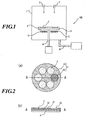
- FIG. 1 is a sectional view showing an exemplary constitution of a general vapor-phase growth apparatus.
- a vapor-phase growth apparatus 100 comprises a reaction furnace 1, a wafer holder 3 for disposing wafers 2 thereon, a susceptor 4 for placing the wafer holder 3 thereon, a heater 5 disposed below the susceptor 4, a rotary mechanism 6 for supporting the wafer holder 3 and the susceptor 4 to allow them to rotate freely, a gas introducing duct 7 for supplying a source gas and a carrier gas therethrough, a gas exhaust duct 8 for discharging the non-reacted gas, and the like.
- FIG. 9 is an enlarged view for showing a detailed construction of the wafer holder 3, where (a) is a plan view, and (b) is a sectional view taken along the line A-A in FIG. 9.
- a plurality of (six in FIG. 2) circular pocket holes 3a are formed for disposing the wafers 2 therein, to be arranged along a single circumference on the surface.
- the other surface of the wafer holder 3 is in contact with the susceptor 4.
- the wafer holder 3 may be composed of one or more members. Generally, it is composed of a single member, as shown in FIG 9.
- the susceptor 4 herein is made of a material having a large coefficient of thermal conductivity (e.g., molybdenum) in order to uniformly transfer heat from the heater 5. It is also general to use graphite, molybdenum or the like, having a large coefficient of thermal conductivity for the wafer holder 3.
- a material having a large coefficient of thermal conductivity e.g., molybdenum
- graphite, molybdenum or the like having a large coefficient of thermal conductivity for the wafer holder 3.
- vapor-phase growth apparatus having such a structure described above, heat is transferred to the wafer 2 through the susceptor 4 and wafer holder 3 by heating the susceptor 4 from the lower side thereof by using the heater 5, to thereby heat the wafer 2 up to a predetermined temperature.
- Vapor-phase growth of a thin film is carried out by rotating the susceptor 4 at a predetermined number of rotation with the aid of a rotating mechanism 6 while uniformly supplying source gas and carrier gas, introduced through a gas introducing duct 7 toward the front surface of the wafer 2.
- An object of the invention is therefore to provide a vapor-phase growth apparatus and a vapor-phase growth method which are capable of allowing a thin film to grow in a vapor phase so as to achieve a desirable uniformity over the entire surface of a wafer.
- the vapor-phase growth apparatus comprises: at least a reaction furnace which can be tightly closed, a wafer container which is disposed in the reaction furnace, for disposing a wafer at a predetermined position thereon, a gas supply member for supplying a source gas toward the wafer, and a.heating member for heating the wafer; the apparatus being designed to form a grown film on a front surface of the wafer by heating the wafer in the reaction furnace through the wafer container while supplying the source gas in a high temperature state, wherein the wafer container comprises: a heat flow control section having a space formed, for disposing a wafer therein; and a heat flow transmitting section which is joined to the heat flow control section, for transmitting heat to the wafer disposed in the space, and a uniform heat resistance R g exists between flat or curved surfaces, of the heat flow control section and the heat flow transmitting section, in close proximity to each other.
- R 1 is a heat resistance in a heat transfer route from a rear surface of the heat flow transmitting section to the front surface of the wafer
- R 2 is a heat resistance in a heat transfer route from the rear surface of the heat flow transmitting section to a front surface of the heat flow control section.
- the heat resistance ratio R 2 /R 1 is not less than 0.8 and not more than 1.2.
- the heat resistance R g is not less than 1.0x10 -6 m 2 K/W and not more than 5.0x10 -3 m 2 K/W; otherwise a clearance distance between the heat flow control section and the heat flow transmitting section may be approximately uniform and in a range of 0.001mm to 1mm. Accordingly, because the heat resistance R g comes to be approximately equal to the contact heat resistance between the heat flow transmitting section and the wafer, it is possible to adjust the ratio R 2 /R 1 easily.
- the heat flow control section is made of a material having a coefficient of thermal conductivity which is not less than 0.5 times that of the wafer disposed on the heat flow transmitting section and not more than 20 times thereof.
- the heat flow control section 31 may be made of any material, as far as the material has characteristics giving no adverse effect on thin film growth or on the environment of the reactor.
- the heat flow transmitting section is made of a material having a coefficient of thermal conductivity higher than that of wafer, for example, a material having a coefficient of thermal conductivity which is not less than 50W/mK and not more than 450W/mK.
- the heat flow control section may be made of any one of amorphous carbon, aluminum nitride, graphite, silicon, silicon carbide, molybdenum, pyrolitec boron nitride, and alumina; and the heat flow transmitting section may be made of any one of molybdenum, graphite, gold, and silver.
- a vapor-phase growth apparatus comprising the above described structure is made to form a grown film on a front surface of the wafer by heating the wafer in the reaction furnace through the wafer container while supplying the source gas in a high temperature state, wherein a temperature difference between a front surface of the wafer container and a front surface of the wafer during growing a thin film in vapor-phase is within 2°C. Accordingly, because it is possible to keep a uniform in-plane temperature distribution of the wafer, a thin film having a desirable uniformity can be grown in the vapor phase over the entire surface of the wafer.
- the present inventors placed a focus on the difference between heat transfer routes inside the wafer 2 and wafer holder 3. That is, the present inventors considered that because the wafer 2 and wafer holder 3 generally differ from each other in materials, so that the same heat transfer cannot be performed in the routes. This causes a difference between achievable surface temperatures of the wafer and the wafer holder.
- FIG. 10 is a schematic view showing heat resistances in the wafer 2 and wafer holder 3.
- T up denotes rear surface temperature of the wafer holder 3
- T surf denotes a front surface temperature of the wafer 2 or wafer holder 3
- T down denotes a temperature at an imaginary plane (referred to as "virtual boundary plane", hereinafter) set at a position being away from the surfaces of the wafer 2 and wafer holder 3 by a predetermined distance.
- V imaginary plane
- heat transfer toward the front surface of the wafer 2 is established along a heat transfer route 1 which originates from the rear surface of the wafer holder 3 and is directed through the wafer holder 3 itself and the wafer 2 to reach the virtual boundary plane
- heat transfer toward the front surface of the wafer holder 3 is established along a heat transfer route 2 which originates from the rear surface of the wafer holder 3 and is directed through the wafer holder 3 itself to reach the virtual boundary plane.
- the wafer 2 and wafer holder 3 differ from each other in the heat transfer route toward the respective surfaces thereof.
- the heat resistance R 1 for the heat transfer route 1 is equal to the sum of heat resistance R 1c for the portion of wafer holder 3, the contact heat resistance R 1g between the wafer holder 3 and wafer 2, and the heat resistance R 1w for the portion of wafer 2; and the heat resistance R 2 for the heat transfer route 2 is equal to the heat resistance R 2c for the portion of wafer holder 3.
- heat resistance R is given by the equation
- the present inventors therefore studied a method of reducing the difference between the surface temperature T 1surf of the wafer 2 and the surface temperature T 2surf of the wafer holder 3, and based on the above equations (5) to (10), and reached an idea that close equalization of the heat resistances R 1 and R 2 in the individual heat transfer routes would be successful (that is, to set heat resistance ratio R 2 /R 1 close to 1).
- the present inventors has found a method in which the wafer holder 3 is composed of two members, i.e., a heat flow control section 31 and a heat flow transmitting section 32.
- R 1 and R 2 are given by the equations below:
- the present invention has been developed based on the aforementioned findings, and is to provide a vapor-phase growth apparatus 100 in which the wafer holder 3 includes: a heat flow control section having a space formed, for disposing a wafer 2 therein; and a heat flow transmitting section which is joined to the heat flow control section, for transmitting heat to the wafer disposed in the space, and a uniform heat resistance R 2g exists between flat or curved surfaces, of the heat flow control section and the heat flow transmitting section, in close proximity to each other, so that the ratio R 2 /R 1 , is not less than 0.8 and not more than 1.2.
- the heat resistance Rg may be not less than 1.0x10 -6 m 2 K/W and not more than 5.0x10 -3 m 2 K/W; otherwise a clearance distance between the heat flow control section and the heat flow transmitting section may be approximately uniform and in a range of 0.001mm to 1mm. Accordingly, it is possible to obtain approximately equal contact heat resistances R 1g and R 2g .
- the heat flow control section may be made of a material having a coefficient of thermal conductivity which is not less than 0.5 times that of the wafer disposed on the heat flow transmitting section and not more than 20 times thereof, to bring the value of coefficient of thermal conductivity k 1w of the wafer 2 near the value of coefficient of thermal conductivity k 2p of the heat flow control section 31.
- the heat resistance ratio R 2 /R 1 can be approximated to 1 also by raising a value of L w or L c in the equations (12) and (13), this is less feasible due to problems in temperature control, in space efficiency of the apparatus and in costs, so that a material of the heat flow control section 31 was selected such as one having a coefficient of thermal conductivity close to that of the wafer 2, as a more practical strategy.
- FIG. 1 is a sectional view showing a schematic construction of the vapor-phase growth apparatus according to the present embodiment.
- FIG. 2 is an enlarged view showing a detailed construction of the wafer holder 3 in the present invention, where (a) is a plan view, and (b) is a sectional view taken along the line A-A.
- the wafer holder 3 which is a wafer container was made of a material having a large coefficient of thermal conductivity, such as graphite.
- the vapor-phase growth apparatus of the embodiment is different from the earlier development in that the wafer container comprises: a heat flow transmitting section 32 made of a material having a large coefficient of thermal conductivity, such as graphite; and a heat flow control section 31 made of amorphous carbon (abbreviated as ⁇ -carbon, hereinafter) or the like, having a coefficient of thermal conductivity relatively near that of the wafer.
- a heat flow transmitting section 32 made of a material having a large coefficient of thermal conductivity, such as graphite
- a heat flow control section 31 made of amorphous carbon (abbreviated as ⁇ -carbon, hereinafter) or the like, having a coefficient of thermal conductivity relatively near that of the wafer.
- the vapor-phase growth apparatus 100 comprises a reaction furnace 1, a wafer holder 3 for disposing wafers 2 thereon, a susceptor 4 for placing the wafer holder 3 thereon, a heater 5 disposed below the susceptor 4, a rotary mechanism 6 for supporting the wafer holder 3 and the susceptor 4 in a freely rotatable manner, a gas introducing duct 7 for supplying a source gas and a carrier gas therethrough, and a gas exhaust duct 8 for discharging the non-reacted gas.
- Each of wall members of the vapor-phase growth apparatus 100 is typically composed of a stainless steel.
- the gas introducing duct 7 is disposed at the vicinity of the center portion of the upper wall member, and introduces a Group XIII (IIIB) source gas such as trimethyl indium (TMI), trimethyl aluminum (TMAl) or trimethyl gallium (TMG); a Group XV (VB) source gas such as arsine (AsH 3 ) or phosphine (PH 3 ); and an inert gas such as hydrogen (H 2 ) as a carrier gas into the reaction furnace.
- a Group XIII (IIIB) source gas such as trimethyl indium (TMI), trimethyl aluminum (TMAl) or trimethyl gallium (TMG)
- a Group XV (VB) source gas such as arsine (AsH 3 ) or phosphine (PH 3 )
- an inert gas such as hydrogen (H 2 ) as a carrier gas into the reaction furnace.
- the wafer holder 3 is composed of a member which comprises a heat flow transmitting section 32 made of graphite and formed in a disk shape, and a heat flow control section 31 made of amorphous carbon which is formed on the heat flow transmitting section 32 as a body.
- the wafer holder 3 is placed on the susceptor 4.
- a plurality of (six in FIG. 2) circular pocket holes (recesses) 3a for containing the wafers 2 therein, are formed along a single circumference.
- the susceptor 4 is composed of a material having a large coefficient of thermal conductivity (e.g. molybdenum) in order to uniformly transfer heat from the heater 5, and is supported by the rotary mechanism 6 in a freely rotatable manner. Below the susceptor 4, the heater 5 for heating the wafer 2 is concentrically arranged.
- the wafer holder 3 in the vapor-phase growth apparatus 100 comprises a heat flow transmitting section 32 made of graphite, and a heat flow control section 31 made of ⁇ -carbon.
- the coefficient of thermal conductivity of the wafer 2 placed on the wafer holder 3 and the coefficient of thermal conductivity of the wafer holder 3 come to be approximately equal to each other. Because the coefficient of thermal conductivity of an InP wafer is 14.3 W/m ⁇ K which is estimated as approximately 0.7 times that of ⁇ -carbon.
- the clearance between the heat flow control section 31 and the heat flow transmitting section 32 is approximately uniform in a range of 0.01mm to 1mm, and the contact heat resistance thereof is not less than 1.0x10 -6 m 2 K/W and not more than 1.0x10 -1 m 2 K/W.
- the heat flow transmitting section 32 may be made of not only graphite but also, for example, molybdenum, gold, silver or the like.
- the heat flow control section 31 may be made of not only ⁇ -carbon but also aluminum nitride, graphite, silicon, silicon carbide, molybdenum, pyrolitec boron nitride, alumina or the like.
- the gas exhaust duct 8 is disposed at the bottom of the reaction furnace 1.
- a source gas introduced into the reaction furnace 1 from an introduction port through the gas introducing duct 7 is decomposed in the upstream side of the reaction furnace, and is then flown to the downstream side to form a thin film on the wafers 2.
- the non-reacted source gas is discharged out through an exhaust port and the gas exhaust duct 8, together with the carrier gas.
- water-cooled jackets are provided typically on the outer periphery of the rotary mechanism 6 and on the lower outside wall of the reaction furnace. These water-cooled jackets and heater 5 control the temperature inside the reaction furnace 1.
- vapor-phase growth apparatus 100 having the above-described construction, heat is transferred to the wafer 2 through the susceptor 4 and the wafer holder 3 under heating of the susceptor 4 from the lower side thereof by using heater 5, to thereby heat the wafer 2 to a predetermined temperature.
- Vapor-phase growth of a thin film is carried out by rotating the susceptor 4 at a predetermined number of rotation with the aid of a rotating mechanism 6 while uniformly supplying a source gas and carrier gas introduced through a gas introducing duct 7 to the upper surface of the wafers 2.
- a wafer holder 3 which includes a heat flow transmitting section 32 made of graphite and a heat flow control section 31 made of ⁇ -carbon, was used in the embodiment, and a graphite-made wafer holder 3 was used in a comparative embodiment.
- FIG. 4 is a schematic analytical model view showing a region around the wafer 2 and wafer holder 3 (having an outward width of 10 mm from the periphery of wafer) of the vapor-phase growth apparatus 100.
- a distance from the bottom surface of the wafer holder 3 to the wafer 2 was defined as 6.4 mm.
- the wafer 2 was an InP wafer having a thickness of 0.5 mm and an inner diameter of 50 mm (2 inches), and the reaction furnace 1 was conditioned to have a hydrogen atmosphere.
- the number of meshes for the analysis was defined as about 6,000,000 meshes.
- the contact heat resistance (R 1g ) between the wafer 2 and the heat flow transmitting section 32, and the contact heat resistance (R 2g ) between the heat flow control section 31 and the heat flow transmitting section 32 were defined as 2.0 ⁇ 10 -4 m 2 K/W. It is to be noted that the contact heat resistance R 1g is affected by the flatness, surface roughness and coefficient of thermal diffusion of the material, of the members contacting with each other, and it can further be reduced by reducing the distance between the contact surfaces.
- the analytical conditions further includes boundary conditions of 45°C for the boundary plane of hydrogen gas located 35 mm above the wafer 2, and of 650 °C for the boundary (rear surface) of the wafer holder 3.
- FIG. 5 shows an analytical result of temperature distribution within the wafer 2 and wafer holder 3 in an Example where a wafer holder 3 comprising a heat flow control section and a heat flow transmitting section is used
- FIG. 6 shows an analytical result of temperature distribution within the wafer 2 and wafer holder 3 in a Comparative Example where an ⁇ -carbon-made wafer holder 3 is used. It is to be noted that FIGS. 5 and 6 show enlarged views of the boundary portion between the wafer 2 and wafer holder 3 in order to clarify the analytical results.
- FIG. 7 shows analytical results of surface temperature distribution of the wafer 2 and wafer holder 3 in the Example
- FIG. 8 shows analytical results of surface temperature distribution of the wafer 2 and wafer holder 3 in the Comparative Example. It is to be noted that FIGS. 7 and 8 show the surface temperature measured at positions along the direction of diameter assuming the center of the wafer as zero.
- Example 5 As shown in FIG. 5, the temperature gradients in the wafer 2 and the heat flow transmitting section 32 are almost equivalent, and a parallel and uniform isothermal lines distribution is observed in the wafer 2.
- Comparative Example as shown in FIG. 6, the temperature gradients in the wafer 2 and the upper portion of the wafer holder 3 are quite different from each other. In the wafer 2, temperature increases toward the peripheral portion from the central portion. This indicates that, in Example, similar heat transfer is established even if the heat transfer route differs.
- Heat resistance ratio R 2 /R 1 was found to be 1.06 in Example, but 0.24 in Comparative Example.
- Example shown in FIG. 7 each of the front surface temperatures of the wafer and of the wafer holder (heat flow control section) was the same at 634.0°C, whereas it was found for Comparative Example shown in FIG. 8 that the front surface temperature of the wafer was 636.0°C, and the front surface temperature of the wafer holder was 638.0°C. That is, the difference between them is about 2.0°C. It was thus made clear that the present Example showed a smaller difference in the front surface temperatures between the circumferential portion (22 to 25 mm) and the central portion (around 0) of the wafer 2, and that the in-plane temperature distribution of the wafer 2 was improved to attain uniformity.
- Example was successful in keeping uniformity of the in-plane temperature distribution of the wafer 2 because the surface temperature in the circumferential portion of the wafer 2 became less likely to be affected by the surface temperature of the wafer holder 3.
- the present invention is successful in proceeding vapor-phase growth of a thin film which has a desirable uniformity over the entire surface of the wafer.
- the wafer container comprises: a heat flow control section having a space formed, for disposing a wafer therein; and a heat flow transmitting section which is joined to the heat flow control section, for transmitting heat to the wafer disposed in the space; and the contact heat resistance between the heat flow transmitting section and the heat flow control section is not less than 1.0x10 -6 m 2 K/W and not more than 5.0x10 -3 m 2 K/W, and the heat flow control section is made of a material having a coefficient of thermal conductivity which is not less than 0.5 times that of the wafer disposed on the heat flow transmitting section and not more than 20 times thereof.
- the present invention is successful in proceeding vapor-phase growth of a thin film which has a desirable uniformity over the entire surface of the wafer.
- the present invention is by no means limited to the above type, and instead applicable to any general vapor-phase growth apparatuses such as those based on face-down system, lateral type, autorotation/revolution system, and the like.
- the present invention is applicable not only to the case where InP wafer is used, but also to cases where a thin film is grown on wafers such as being comprised of Si, GaAs, GaN, sapphire, glass, ceramic, and the like. In these cases, it is also allowable to alter a material composing the wafer holder 3 (or heat flow control section 31) depending on the wafer to be used.
Landscapes
- Chemical & Material Sciences (AREA)
- Chemical Kinetics & Catalysis (AREA)
- General Chemical & Material Sciences (AREA)
- Engineering & Computer Science (AREA)
- Materials Engineering (AREA)
- Metallurgy (AREA)
- Organic Chemistry (AREA)
- Crystallography & Structural Chemistry (AREA)
- Mechanical Engineering (AREA)
- Chemical Vapour Deposition (AREA)
- Crystals, And After-Treatments Of Crystals (AREA)
Applications Claiming Priority (5)
| Application Number | Priority Date | Filing Date | Title |
|---|---|---|---|
| JP2002172407 | 2002-06-13 | ||
| JP2002172407 | 2002-06-13 | ||
| JP2002238207A JP3882141B2 (ja) | 2002-06-13 | 2002-08-19 | 気相成長装置および気相成長方法 |
| JP2002238207 | 2002-08-19 | ||
| PCT/JP2002/010714 WO2003107404A1 (ja) | 2002-06-13 | 2002-10-16 | 気相成長装置および気相成長方法 |
Publications (3)
| Publication Number | Publication Date |
|---|---|
| EP1533834A1 true EP1533834A1 (de) | 2005-05-25 |
| EP1533834A4 EP1533834A4 (de) | 2007-01-17 |
| EP1533834B1 EP1533834B1 (de) | 2013-11-20 |
Family
ID=29738383
Family Applications (1)
| Application Number | Title | Priority Date | Filing Date |
|---|---|---|---|
| EP02807525.7A Expired - Lifetime EP1533834B1 (de) | 2002-06-13 | 2002-10-16 | Dampfphasenepitaxialvorrichtung und dampfphasenepitaxialverfahren |
Country Status (8)
| Country | Link |
|---|---|
| US (1) | US7314519B2 (de) |
| EP (1) | EP1533834B1 (de) |
| JP (1) | JP3882141B2 (de) |
| KR (1) | KR100632454B1 (de) |
| CN (1) | CN1322551C (de) |
| CA (1) | CA2486664C (de) |
| TW (1) | TWI254979B (de) |
| WO (1) | WO2003107404A1 (de) |
Cited By (2)
| Publication number | Priority date | Publication date | Assignee | Title |
|---|---|---|---|---|
| WO2012021370A1 (en) * | 2010-08-13 | 2012-02-16 | Veeco Instruments Inc. | Enhanced wafer carrier |
| CN106133208A (zh) * | 2014-03-27 | 2016-11-16 | 瓦里安半导体设备公司 | 硅熔体中控制热流的装置 |
Families Citing this family (8)
| Publication number | Priority date | Publication date | Assignee | Title |
|---|---|---|---|---|
| WO2005081298A1 (ja) * | 2004-02-25 | 2005-09-01 | Nippon Mining & Metals Co., Ltd. | 気相成長装置 |
| CN1300189C (zh) * | 2005-02-05 | 2007-02-14 | 浙江大学 | 烯烃气相聚合反应在线控制装置及其方法 |
| US20070217119A1 (en) * | 2006-03-17 | 2007-09-20 | David Johnson | Apparatus and Method for Carrying Substrates |
| TW201205713A (en) * | 2010-07-21 | 2012-02-01 | Chi Mei Lighting Tech Corp | Vapor deposition apparatus and susceptor |
| CN102605341A (zh) * | 2011-01-20 | 2012-07-25 | 奇力光电科技股份有限公司 | 气相沉积装置及承载盘 |
| US20120225206A1 (en) * | 2011-03-01 | 2012-09-06 | Applied Materials, Inc. | Apparatus and Process for Atomic Layer Deposition |
| JP2014116331A (ja) * | 2011-11-30 | 2014-06-26 | Dowa Electronics Materials Co Ltd | 結晶成長装置、結晶成長方法及びサセプタ |
| CN103526285B (zh) * | 2013-09-23 | 2016-03-30 | 北京思捷爱普半导体设备有限公司 | 一种led外延片倒置mocvd反应炉 |
Family Cites Families (24)
| Publication number | Priority date | Publication date | Assignee | Title |
|---|---|---|---|---|
| JPS5510436A (en) | 1978-07-05 | 1980-01-24 | Nec Corp | Susceptor for vapor phase crystal growth |
| JPS6190186A (ja) | 1984-10-09 | 1986-05-08 | 株式会社 セガ・エンタ−プライゼス | タイプライテイング練習機 |
| JPS61219130A (ja) | 1985-03-25 | 1986-09-29 | Toshiba Mach Co Ltd | 気相成長装置 |
| JPH0282528A (ja) * | 1988-09-19 | 1990-03-23 | Fujitsu Ltd | プラズマcvd装置 |
| JPH0369113A (ja) | 1989-08-09 | 1991-03-25 | Fujitsu Ltd | 半導体製造装置 |
| DE69126122T2 (de) * | 1990-09-21 | 1997-08-28 | Fujitsu Ltd | Methode und apparat zum wachsen von verbindungshalbleiterkristallen |
| JPH07176482A (ja) | 1991-05-31 | 1995-07-14 | At & T Corp | エピタキシャル成長方法および装置 |
| JP2750331B2 (ja) * | 1992-04-23 | 1998-05-13 | 株式会社ジャパンエナジー | エピタキシャル成長用基板およびエピタキシャル成長方法 |
| JPH06310438A (ja) * | 1993-04-22 | 1994-11-04 | Mitsubishi Electric Corp | 化合物半導体気相成長用基板ホルダおよび化合物半導体気相成長装置 |
| JP3257741B2 (ja) | 1994-03-03 | 2002-02-18 | 東京エレクトロン株式会社 | プラズマエッチング装置及び方法 |
| US5584936A (en) | 1995-12-14 | 1996-12-17 | Cvd, Incorporated | Susceptor for semiconductor wafer processing |
| EP0823492A3 (de) * | 1996-08-07 | 1999-01-20 | Concept Systems Design Inc. | Zonenheizungssystem mit Rückkopplungsreglung |
| KR100203780B1 (ko) * | 1996-09-23 | 1999-06-15 | 윤종용 | 반도체 웨이퍼 열처리 장치 |
| JP3867328B2 (ja) * | 1996-12-04 | 2007-01-10 | ソニー株式会社 | スパッタリングターゲット及びその製造方法 |
| JPH10303288A (ja) | 1997-04-26 | 1998-11-13 | Anelva Corp | プラズマ処理装置用基板ホルダー |
| JPH11180796A (ja) | 1997-12-22 | 1999-07-06 | Japan Energy Corp | 気相成長方法およびその方法を適用した気相成長装置 |
| DE19934336A1 (de) | 1998-09-03 | 2000-03-09 | Siemens Ag | Vorrichtung zum Herstellen und Bearbeiten von Halbleitersubstraten |
| JP2000355766A (ja) | 1999-06-15 | 2000-12-26 | Hitachi Kokusai Electric Inc | 基板処理装置及び基板処理方法 |
| KR100351049B1 (ko) * | 1999-07-26 | 2002-09-09 | 삼성전자 주식회사 | 웨이퍼 가열 방법 및 이를 적용한 장치 |
| JP2002145670A (ja) | 1999-09-06 | 2002-05-22 | Ibiden Co Ltd | 半導体製造・検査装置用セラミック基板 |
| US6900149B1 (en) * | 1999-09-06 | 2005-05-31 | Ibiden Co., Ltd. | Carbon-containing aluminum nitride sintered compact and ceramic substrate for use in equipment for manufacturing or inspecting semiconductor |
| US6878250B1 (en) * | 1999-12-16 | 2005-04-12 | Honeywell International Inc. | Sputtering targets formed from cast materials |
| US6331233B1 (en) * | 2000-02-02 | 2001-12-18 | Honeywell International Inc. | Tantalum sputtering target with fine grains and uniform texture and method of manufacture |
| JP2001230234A (ja) | 2000-02-16 | 2001-08-24 | Hitachi Ltd | プラズマ処理装置及び方法 |
-
2002
- 2002-08-19 JP JP2002238207A patent/JP3882141B2/ja not_active Expired - Lifetime
- 2002-10-16 US US10/515,969 patent/US7314519B2/en not_active Expired - Lifetime
- 2002-10-16 CN CNB028291352A patent/CN1322551C/zh not_active Expired - Lifetime
- 2002-10-16 EP EP02807525.7A patent/EP1533834B1/de not_active Expired - Lifetime
- 2002-10-16 KR KR1020047020271A patent/KR100632454B1/ko not_active Expired - Fee Related
- 2002-10-16 WO PCT/JP2002/010714 patent/WO2003107404A1/ja not_active Ceased
- 2002-10-16 CA CA2486664A patent/CA2486664C/en not_active Expired - Lifetime
-
2003
- 2003-05-28 TW TW092114413A patent/TWI254979B/zh not_active IP Right Cessation
Cited By (4)
| Publication number | Priority date | Publication date | Assignee | Title |
|---|---|---|---|---|
| WO2012021370A1 (en) * | 2010-08-13 | 2012-02-16 | Veeco Instruments Inc. | Enhanced wafer carrier |
| CN106133208A (zh) * | 2014-03-27 | 2016-11-16 | 瓦里安半导体设备公司 | 硅熔体中控制热流的装置 |
| US10415151B1 (en) | 2014-03-27 | 2019-09-17 | Varian Semiconductor Equipment Associates, Inc | Apparatus for controlling heat flow within a silicon melt |
| CN106133208B (zh) * | 2014-03-27 | 2020-04-28 | 瓦里安半导体设备公司 | 用于控制熔体内的热流的装置及其处理方法 |
Also Published As
| Publication number | Publication date |
|---|---|
| JP3882141B2 (ja) | 2007-02-14 |
| TW200400548A (en) | 2004-01-01 |
| CN1322551C (zh) | 2007-06-20 |
| KR100632454B1 (ko) | 2006-10-11 |
| EP1533834A4 (de) | 2007-01-17 |
| CA2486664C (en) | 2010-12-07 |
| TWI254979B (en) | 2006-05-11 |
| CA2486664A1 (en) | 2003-12-24 |
| KR20050012791A (ko) | 2005-02-02 |
| WO2003107404A8 (fr) | 2005-01-06 |
| US7314519B2 (en) | 2008-01-01 |
| JP2004072054A (ja) | 2004-03-04 |
| US20050166836A1 (en) | 2005-08-04 |
| EP1533834B1 (de) | 2013-11-20 |
| CN1628371A (zh) | 2005-06-15 |
| WO2003107404A1 (ja) | 2003-12-24 |
Similar Documents
| Publication | Publication Date | Title |
|---|---|---|
| TWI361847B (en) | Method and equipment for aln-monocrystal production with gas-pervious crucible-wall | |
| US8317449B2 (en) | Multiple substrate transfer robot | |
| TW200845145A (en) | Microbatch deposition chamber with radiant heating | |
| JPS62500624A (ja) | 半導体ウェ−ハ処理のためのリアクタ−装置 | |
| US7314519B2 (en) | Vapor-phase epitaxial apparatus and vapor phase epitaxial method | |
| EP1720200B1 (de) | Epitaxial wachsende einrichtungen | |
| EP0164928A2 (de) | Senkrechter Heisswandreaktor zur chemischen Abscheidung aus der Gasphase | |
| US7344597B2 (en) | Vapor-phase growth apparatus | |
| JP3418950B2 (ja) | エピタキシャル成長炉 | |
| CN121700366A (zh) | 成膜方法、晶片支承结构以及气相生长装置 | |
| JP2007280974A (ja) | 気相成長装置 |
Legal Events
| Date | Code | Title | Description |
|---|---|---|---|
| PUAI | Public reference made under article 153(3) epc to a published international application that has entered the european phase |
Free format text: ORIGINAL CODE: 0009012 |
|
| 17P | Request for examination filed |
Effective date: 20041227 |
|
| AK | Designated contracting states |
Kind code of ref document: A1 Designated state(s): AT BE BG CH CY CZ DE DK EE ES FI FR GB GR IE IT LI LU MC NL PT SE SK TR |
|
| AX | Request for extension of the european patent |
Extension state: AL LT LV MK RO SI |
|
| DAX | Request for extension of the european patent (deleted) | ||
| RBV | Designated contracting states (corrected) |
Designated state(s): DE FR GB |
|
| RAP1 | Party data changed (applicant data changed or rights of an application transferred) |
Owner name: NIPPON MINING & METALS CO., LTD. |
|
| A4 | Supplementary search report drawn up and despatched |
Effective date: 20061219 |
|
| RIC1 | Information provided on ipc code assigned before grant |
Ipc: H01L 21/205 20060101AFI20040106BHEP Ipc: C30B 25/12 20060101ALI20061212BHEP |
|
| 17Q | First examination report despatched |
Effective date: 20070717 |
|
| REG | Reference to a national code |
Ref country code: DE Ref legal event code: R079 Ref document number: 60245795 Country of ref document: DE Free format text: PREVIOUS MAIN CLASS: H01L0021205000 Ipc: C30B0025100000 |
|
| GRAP | Despatch of communication of intention to grant a patent |
Free format text: ORIGINAL CODE: EPIDOSNIGR1 |
|
| RIC1 | Information provided on ipc code assigned before grant |
Ipc: C30B 25/12 20060101ALI20130628BHEP Ipc: C30B 25/10 20060101AFI20130628BHEP Ipc: C23C 16/46 20060101ALI20130628BHEP |
|
| INTG | Intention to grant announced |
Effective date: 20130806 |
|
| GRAS | Grant fee paid |
Free format text: ORIGINAL CODE: EPIDOSNIGR3 |
|
| GRAA | (expected) grant |
Free format text: ORIGINAL CODE: 0009210 |
|
| AK | Designated contracting states |
Kind code of ref document: B1 Designated state(s): DE FR GB |
|
| REG | Reference to a national code |
Ref country code: GB Ref legal event code: FG4D |
|
| REG | Reference to a national code |
Ref country code: DE Ref legal event code: R081 Ref document number: 60245795 Country of ref document: DE Owner name: JX NIPPON MINING & METALS CORP., JP Free format text: FORMER OWNER: NIKKO MATERIALS CO., LTD., TOKIO/TOKYO, JP |
|
| REG | Reference to a national code |
Ref country code: DE Ref legal event code: R096 Ref document number: 60245795 Country of ref document: DE Effective date: 20140116 |
|
| REG | Reference to a national code |
Ref country code: DE Ref legal event code: R097 Ref document number: 60245795 Country of ref document: DE |
|
| PLBE | No opposition filed within time limit |
Free format text: ORIGINAL CODE: 0009261 |
|
| STAA | Information on the status of an ep patent application or granted ep patent |
Free format text: STATUS: NO OPPOSITION FILED WITHIN TIME LIMIT |
|
| 26N | No opposition filed |
Effective date: 20140821 |
|
| REG | Reference to a national code |
Ref country code: DE Ref legal event code: R097 Ref document number: 60245795 Country of ref document: DE Effective date: 20140821 |
|
| REG | Reference to a national code |
Ref country code: FR Ref legal event code: PLFP Year of fee payment: 14 |
|
| REG | Reference to a national code |
Ref country code: FR Ref legal event code: PLFP Year of fee payment: 15 |
|
| REG | Reference to a national code |
Ref country code: DE Ref legal event code: R081 Ref document number: 60245795 Country of ref document: DE Owner name: JX NIPPON MINING & METALS CORP., JP Free format text: FORMER OWNER: NIPPON MINING & METALS CO., LTD., TOKYO, JP |
|
| REG | Reference to a national code |
Ref country code: GB Ref legal event code: 732E Free format text: REGISTERED BETWEEN 20170525 AND 20170531 |
|
| REG | Reference to a national code |
Ref country code: FR Ref legal event code: PLFP Year of fee payment: 16 |
|
| REG | Reference to a national code |
Ref country code: FR Ref legal event code: CA Effective date: 20171003 Ref country code: FR Ref legal event code: CD Owner name: JX NIPPON MINING & METALS CORPORATION, JP Effective date: 20171003 Ref country code: FR Ref legal event code: TP Owner name: JX NIPPON MINING & METALS CORPORATION, JP Effective date: 20171003 |
|
| REG | Reference to a national code |
Ref country code: FR Ref legal event code: CA Effective date: 20171006 |
|
| REG | Reference to a national code |
Ref country code: FR Ref legal event code: PLFP Year of fee payment: 17 |
|
| PGFP | Annual fee paid to national office [announced via postgrant information from national office to epo] |
Ref country code: DE Payment date: 20211020 Year of fee payment: 20 Ref country code: GB Payment date: 20211022 Year of fee payment: 20 |
|
| PGFP | Annual fee paid to national office [announced via postgrant information from national office to epo] |
Ref country code: FR Payment date: 20211021 Year of fee payment: 20 |
|
| REG | Reference to a national code |
Ref country code: DE Ref legal event code: R071 Ref document number: 60245795 Country of ref document: DE |
|
| REG | Reference to a national code |
Ref country code: GB Ref legal event code: PE20 Expiry date: 20221015 |
|
| PG25 | Lapsed in a contracting state [announced via postgrant information from national office to epo] |
Ref country code: GB Free format text: LAPSE BECAUSE OF EXPIRATION OF PROTECTION Effective date: 20221015 |