EP1520288B1 - Multirate processing for metrology of plasma rf source - Google Patents
Multirate processing for metrology of plasma rf source Download PDFInfo
- Publication number
- EP1520288B1 EP1520288B1 EP03721634.8A EP03721634A EP1520288B1 EP 1520288 B1 EP1520288 B1 EP 1520288B1 EP 03721634 A EP03721634 A EP 03721634A EP 1520288 B1 EP1520288 B1 EP 1520288B1
- Authority
- EP
- European Patent Office
- Prior art keywords
- digital
- signals
- generator
- frequency
- signal
- Prior art date
- Legal status (The legal status is an assumption and is not a legal conclusion. Google has not performed a legal analysis and makes no representation as to the accuracy of the status listed.)
- Expired - Lifetime
Links
Images


Classifications
-
- H—ELECTRICITY
- H01—ELECTRIC ELEMENTS
- H01J—ELECTRIC DISCHARGE TUBES OR DISCHARGE LAMPS
- H01J37/00—Discharge tubes with provision for introducing objects or material to be exposed to the discharge, e.g. for the purpose of examination or processing thereof
- H01J37/32—Gas-filled discharge tubes
- H01J37/32009—Arrangements for generation of plasma specially adapted for examination or treatment of objects, e.g. plasma sources
- H01J37/32082—Radio frequency generated discharge
- H01J37/32174—Circuits specially adapted for controlling the RF discharge
-
- H—ELECTRICITY
- H03—ELECTRONIC CIRCUITRY
- H03H—IMPEDANCE NETWORKS, e.g. RESONANT CIRCUITS; RESONATORS
- H03H17/00—Networks using digital techniques
- H03H17/02—Frequency selective networks
- H03H17/06—Non-recursive filters
- H03H17/0621—Non-recursive filters with input-sampling frequency and output-delivery frequency which differ, e.g. extrapolation; Anti-aliasing
- H03H17/0635—Non-recursive filters with input-sampling frequency and output-delivery frequency which differ, e.g. extrapolation; Anti-aliasing characterized by the ratio between the input-sampling and output-delivery frequencies
- H03H17/0671—Cascaded integrator-comb [CIC] filters
-
- H—ELECTRICITY
- H05—ELECTRIC TECHNIQUES NOT OTHERWISE PROVIDED FOR
- H05H—PLASMA TECHNIQUE; PRODUCTION OF ACCELERATED ELECTRICALLY-CHARGED PARTICLES OR OF NEUTRONS; PRODUCTION OR ACCELERATION OF NEUTRAL MOLECULAR OR ATOMIC BEAMS
- H05H1/00—Generating plasma; Handling plasma
- H05H1/24—Generating plasma
- H05H1/46—Generating plasma using applied electromagnetic fields, e.g. high frequency or microwave energy
Definitions
- the present invention relates generally to RF plasma systems which employ frequency tunable sources and, more particularly, to a multirate signal processing technique that tracks the tuned frequency of an RF generator and effectively removes undesirable frequency components.
- plasma etching has become an integral part of the manufacture of semiconductor circuits.
- etchers are frequently used in semiconductor processing when a relatively straight vertical edge is needed.
- undercutting the polysilicon can adversely affect the operation of the transistor.
- Undercutting is frequently encountered when a liquid etching method is used.
- plasma etching which uses ions accelerated by an electric field, tends to etch only horizontal exposed surfaces and therefore avoids undercutting.
- the RF power delivered to a plasma chamber typically includes multiple fundamental frequencies as well as corresponding harmonic tones.
- the voltage applied to the plasma chamber may have fundamental frequencies at both 2 MHz and 27 MHz, where the 2 MHz signal includes harmonics at 4 MHz, 6 MHz, 8MHz, etc.
- the 27 MHz signal may include intermodulation products at 25 MHz, 23 MHz, etc. This is significant because the knowledge of the amount of energy delivered by the source(s) may be distorted by harmonic tones or intermodulation products thus requiring the limitation or elimination of these frequencies for an accurate measurement.
- Multirate processing possess significant processing gain to significantly reduce the undesirable frequency components. Processing gain is the rejection of out of band noise. This occurs when the frequency of interest occupies less bandwidth than the input signal.
- the present invention provides a multirate signal processing, technique that tracks the tuned frequency of an RF generator, thereby effectively removing undesirable frequency components from the frequency of interest.
- This approach significantly relaxes the design specifications of any filtering elements between the sensor and signal processing unit.
- This approach also has the immediate benefit of improved accuracy and a reduced footprint.
- This approach is also adaptable to a variety of RF sensors.
- the present invention is also significant with regard to RF plasma systems employing frequency tunable sources.
- a RF generator in a frequency tunable system adjusts its frequency to maximize power transfer.
- the bandpass region of the metrology also has to shift accordingly for the tuned frequency to pass the frequency of interest and remove the others.
- the present invention coherently tracks the tune frequency of the RF generator.
- An additional benefit from the present invention is realized in plasma systems that utilize multiple RF frequency sources. It is often the case in multiple RF frequency sources that intermodulation products exist in the frequency band of the metrology circuit. This will result when the metrology of the high frequency RF source bandwidth is greater than the intermodulation product of the frequency sources.
- a multirate processing scheme provides significant attenuation to out of band signals to eliminate the effect of these intermodulation products on the accuracy of the metrology.
- EP 1244133 discloses a radio frequency (RF) probe analysis system having a broadband design.
- the analysis system includes a sampling unit for generating digital power signals based on a plurality of analog signals.
- the analog signals characterize power delivered from an RF power delivery system to a plasma chamber.
- the analysis system further includes a digital processing unit for generating a digital spectrum signal based on the digital power signals .
- the sampling unit simultaneously samples a first plurality of frequencies from the analog signals such that the digital spectrum signal defines signal levels for the first plurality of frequencies.;
- the sampling unit may also simultaneously sample a second plurality of frequencies from the analog signals such that the digital spectrum signal further defines signal levels for the second plurality of frequencies.
- the broadband architecture of the sampling unit enables closed loop control of power delivered to the camber to tolerances.
- EP 1339086 discloses radio frequency (RF) probe head apparatus provided for measuring voltage and current of an RF signal in a sampled transmission line.
- the probe head apparatus includes a conductive housing, a bus inside the conductive housing, a pair of connectors mounted on the conductive housing and configured to pass an RF signal into and out of the housing via the bus, a voltage pick-up board within the housing, and a current pickup board within the housing.
- the voltage pickup board has an analog processor responsive to an electric field around the bus to produce a first DC output indicative of a root-mean-square (RMS) value of the electric field.
- the current pick-up board has a second analog processor responsive to a magnetic field around the bus to produce a second DC output indicative of an RMS value of the magnetic field.
- an RF generator for use in an RF plasma system.
- the RF generator includes: a power source that is operable to generate RF power signals at a tuned frequency; a sensor unit that is adapted to detect the RF power signals and operable to generate analog signals representative of the RF power signals, where the analog signals include a frequency of interest and a plurality of interfering frequency components; and a sensor signal processing unit that is adapted to receive the analog signals from the sensor unit and to band limit the analog signals within a predefined bandwidth that passes the frequency of interest and rejects interfering frequency components.
- the sensor signal processing unit is preferably implemented in the digital domain.
- FIG. 1 An exemplary single source RF plasma system 10 is depicted in Figure 1 .
- the RF plasma system 10 is comprised of an RF generator 12, a matching network 14 and a plasma chamber 16 as is well known in the art. While the following description is provided with reference to a single source system, it is readily understood that the broader aspects of the present invention are applicable to RF plasma systems having two or more RF generators.
- the RF generator 12 further includes an RF power source 22, an RF sensor 24 and a sensor signal processing unit 26.
- the RF power source 22 is operable to generate RF power signals that are output via the matching network 14 to the plasma chamber 16. It is to be understood that only the primary components of generator are discussed, but that other known components are needed to implement the generator.
- An RF sensor 24 is interposed between the RF power source 22 and the matching network to detect the RF power signals output by the RF power source 22.
- the RF sensor 24 is generally operable to generate analog signals representative of the RF power signals which are in turn used as control signals to the RF power source 22.
- the RF sensor 24 is comprised of a voltage probe and a current probe, such that the sensor outputs represent RF line voltage and RF line current, respectively.
- the RF sensor may be defined as a directional sensor whose outputs correspond to forward power and reflected power. In either case, two output signals from the RF sensor 24 preferably serve as input to the sensor signal processing unit 26.
- the sensor output is connected via a 50-Ohm transmission line to the sensor signal processing unit 26.
- Transmission line selection is arbitrary provided the following principles are adhered to: good waveform fidelity is maintained through careful impedance matching of the line and the termination, and good attenuation of interfering signals is maintained through proper shielding and construction that rejects external electromagnetic interference.
- sensor signal processing is somewhat dependent on the particular sensor configuration, it is readily understood that the broader aspects of the sensor signal processing approach of the present invention is applicable to different types of sensor configurations.
- the sensor signal processing unit 26 is adapted to receive analog signals from the RF sensor and output a digital control signal that tracks the tuned frequency of the RF power signals generated by the RF power source 22. It is understood that the analog signals received from the RF sensor will include a frequency of interest and a plurality of interfering frequency components or other unwanted spurious frequency components. In operation, the sensor signal processing unit 26 band limits the analog signals within a predefined bandwidth that passes the frequency of interest and rejects the interfering frequency components. Although the frequency of interest is preferably the fundamental frequency component at the tuned frequency of the power, it is envisioned that the frequency of interest may also include other frequency components that are related to the tuned frequency. In the case of a tunable RF power source, the predefined bandwidth is adjustable to pass the frequency of interest as will be further described below. It is envisioned that the sensor signal processing unit 26 may be local or remotely located from the RF sensor 24.
- each sensor output is initially filtered by an anti-aliasing filter 32.
- the purpose of the anti-aliasing filters is to band limit the frequency of the signal of interest.
- the minimum bandwidth of the filter is typically equivalent to the operating frequency band of the RF power source. Attenuation of the sensor output signals prior to the filter may be necessary depending on the amplitude of the output signals; otherwise, the design specifications for these anti-aliasing filters 32 are not critical because further band limiting is accomplished during the decimation process.
- Each anti-aliasing filter 32 is in turn connected to a high-speed analog-to-digital (A/D) converter pair 34.
- the A/D converters 34 operate as a pair by simultaneously sampling the respective signal output from each filter.
- the A/D converter pair 34 then converts the analog input signals into corresponding digital power signals.
- the spectral content of the input signals includes frequencies in the passband of the anti-aliasing filter that are within the Nyquist range (1/2 sample rate) or greater. This is achievable because the bandwidth of the converters is greater than the sample rate.
- Output from the A/D converter pair 34 is then connected to a programmable device for large scale integration (LSI).
- a field programmable gate array (FPGA) 36 receives the digital signals output by the A/D converter pair 34.
- the primary purpose of the FPGA 36 is to reduce the sample rate of the A/D converter pair 34 to a data rate manageable by a digital signal processor 38. It is critical that the signal processing unit does not introduce significant group delay in the control loop of the plasma RF generator. Therefore, the basis of the decimation factor is to provide optimal group delay for the control loop and adequate band limiting for sensor measurement accuracy.
- the sensor signal processing unit 26 employs a multirate signal processing technique to achieve effective removal of undesirable frequency components from the frequency of interest as shown in Figure 3 .
- bandwidth of the sensor signal processing unit 26 may be designed to pass a frequency of interest associated with one of the two powers sources and filter spurious frequency components which are caused by intermodulation of the power signals from the two sources.
- the multirate signal processing is preferably implemented in the digital domain using a digital frequency synthesizer 42, a pair of digital mixing modules 44, a pair of decimation modules 46, and a pair of low pass filters 48.
- Digital signals acquired from the A/D converter pair 34 are applied to a pair of digital mixing modules 44.
- Each digital mixing module 44 also receives two inputs from the digital frequency synthesizer 42.
- the digital frequency synthesizer 42 generates digital mixing signals.
- the digital frequency synthesizer produces a sine and cosine waveform representative of the frequency setpoint, where the frequency setpoint correlates to the frequency of interest.
- the frequency setpoint is a frequency offset received from the frequency source that drives the RF power source.
- the frequency tracking technique is coherent. It is readily understood that other coherent frequency tracking techniques as well as various autonomous frequency tracking techniques are within the scope of the present invention.
- Each digital mixing module 44 is operable to combine digital mixing signals received from the digital frequency synthesizer 42 with the digital power signals received from the A/D converter pair 34. To do so, each digital mixing module includes two digital multipliers. In addition, the digital mixing modules 44 operates at the sample rate as the A/D converter pair 34. The result from each digital mixing module 44 is a spectrum constructed from the sum and difference of the frequencies contained in the sampled input signals and the signals provided by the digital frequency synthesizer.
- decimation is a well known process for decreasing the data rate of a signal.
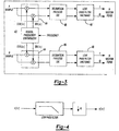
- a conventional decimator scheme is depicted in Figure 4 . Although this is an acceptable method for decimation, this scheme embodies various constraints that make it difficult to implement. These constraints include the number of high speed multipliers is equal to the order of the low pass filter, storage requirements for the filter coefficients, and local timing is critical for the low pass filter implementation.
- FIG. 5 An alternative decimation scheme is depicted in Figure 5 .
- decimation is achieved via a cascade integrator comb (CIC) filter 40.
- the frequency response of the CIC filter 40 is dependent on the design parameters K, N and R.
- K yields the number of stages for the filter.
- the filter is preferably symmetrical such that for a given K there are K integrator stages and K comb filter stages.
- N is the delay element in the feedback of the comb filter.
- R is the decimation factor.
- the sample rate is reduced to a data rate of (sample rate/R).
- a plot of the frequency response for various decimation factors for a 5th order CIC filter, where the delay element N is 1, is shown in Figure 6 .
- the decimation factor increases, the data rate is proportionally reduced and bandlimiting increased.
- other decimation schemes e.g., polyphase decomposition
- a pair of low pass filters 48 immediately follows the decimation process.
- the low pass filters provide a shaping function of the spectral output of the CIC filter 40. For example, a nineteen (19) tap halfband filter may be used for this purpose.
- Output is shown as an in-phase (I) signal and a quadrature (Q) signal for each of the digital power signals input into the sensor signal processing unit 26. It is readily understood that these output signals may serve as control feedback signals for the PR power source 22. It is further understood that other types of control feedback signals may be derived from these output signals and the type of control feedback signal may depend on the type of sensor 24 employed by the RF generator 12.
- the frequency setpoint is derived by taking the derivative of output of either sampled input signal with respect to time.
- the results of this derivative provides the rate of rotation through the complex coordinate system. This rate is directly proportional to the decimated frequency for the difference between the frequency of interest contained in the sampled input signals and the digital frequency synthesizer.
- the setpoint of the digital frequency synthesizer is adjusted to maintain the frequency of interest in CIC filter passband.
- the derived frequency could also be a filtered version of the derivatives of each output of either sampled input signal with respect to time. For instance the derivative would be calculated with respect to time for each output signal and then filtered by a linear (average) or nonlinear (median) filter.
- the above described signal processing approach may be implemented in a programmable digital signal processor, a programmable device for large scale integration or a combination thereof.
- the LSI approach is preferable for the speed obtained by parallel processing; whereas the DSP approach is preferred for conversion of data and for applying the appropriate calibration factors.
- the present invention provides an effective and efficient narrow passband filter to eliminate distortion in the measurement of sensor signals. Intermodulation products and environmental noise associated with an RF plasma system are significantly attenuated.
- the proposed implementation efficiently uses digital logic, thereby leading to a smaller footprint. A comparable analog approach often requires component adjustments and/or different components.
- the proposed digital implementation will also have minimal long-term drift and is easily adaptable to different applications.
Landscapes
- Physics & Mathematics (AREA)
- Engineering & Computer Science (AREA)
- Plasma & Fusion (AREA)
- Chemical & Material Sciences (AREA)
- Analytical Chemistry (AREA)
- Computer Hardware Design (AREA)
- Mathematical Physics (AREA)
- Electromagnetism (AREA)
- Spectroscopy & Molecular Physics (AREA)
- Plasma Technology (AREA)
- Drying Of Semiconductors (AREA)
Applications Claiming Priority (3)
| Application Number | Priority Date | Filing Date | Title |
|---|---|---|---|
| US10/192,196 US6707255B2 (en) | 2002-07-10 | 2002-07-10 | Multirate processing for metrology of plasma RF source |
| US192196 | 2002-07-10 | ||
| PCT/US2003/011266 WO2004008502A2 (en) | 2002-07-10 | 2003-04-14 | Multirate processing for metrology of plasma rf source |
Publications (2)
| Publication Number | Publication Date |
|---|---|
| EP1520288A2 EP1520288A2 (en) | 2005-04-06 |
| EP1520288B1 true EP1520288B1 (en) | 2018-10-17 |
Family
ID=30114293
Family Applications (1)
| Application Number | Title | Priority Date | Filing Date |
|---|---|---|---|
| EP03721634.8A Expired - Lifetime EP1520288B1 (en) | 2002-07-10 | 2003-04-14 | Multirate processing for metrology of plasma rf source |
Country Status (7)
| Country | Link |
|---|---|
| US (1) | US6707255B2 (enExample) |
| EP (1) | EP1520288B1 (enExample) |
| JP (2) | JP2005532668A (enExample) |
| KR (1) | KR100738990B1 (enExample) |
| CN (1) | CN100339943C (enExample) |
| AU (1) | AU2003224937A1 (enExample) |
| WO (1) | WO2004008502A2 (enExample) |
Families Citing this family (38)
| Publication number | Priority date | Publication date | Assignee | Title |
|---|---|---|---|---|
| US20060060139A1 (en) * | 2004-04-12 | 2006-03-23 | Mks Instruments, Inc. | Precursor gas delivery with carrier gas mixing |
| JP2008527378A (ja) * | 2005-01-11 | 2008-07-24 | イノベーション エンジニアリング、エルエルシー | 負荷に供給されたrf電力およびその負荷の複素インピーダンスを検出する方法 |
| US7602127B2 (en) * | 2005-04-18 | 2009-10-13 | Mks Instruments, Inc. | Phase and frequency control of a radio frequency generator from an external source |
| US8102954B2 (en) | 2005-04-26 | 2012-01-24 | Mks Instruments, Inc. | Frequency interference detection and correction |
| US7477711B2 (en) * | 2005-05-19 | 2009-01-13 | Mks Instruments, Inc. | Synchronous undersampling for high-frequency voltage and current measurements |
| US7780814B2 (en) * | 2005-07-08 | 2010-08-24 | Applied Materials, Inc. | Wafer pre-clean reactor cable termination for selective suppression/reflection of source and bias frequency cross products |
| US7196650B1 (en) | 2006-01-27 | 2007-03-27 | Analog Devices, Inc. | Signal converter systems and methods with enhanced signal-to-noise ratios |
| US7788309B2 (en) * | 2006-04-04 | 2010-08-31 | Analog Devices, Inc. | Interleaved comb and integrator filter structures |
| US7408495B2 (en) * | 2006-05-15 | 2008-08-05 | Guzik Technical Enterprises | Digital equalization of multiple interleaved analog-to-digital converters |
| US8055203B2 (en) * | 2007-03-14 | 2011-11-08 | Mks Instruments, Inc. | Multipoint voltage and current probe system |
| DE102007056468A1 (de) * | 2007-11-22 | 2009-06-04 | Hüttinger Elektronik Gmbh + Co. Kg | Messsignalverarbeitungseinrichtung und Verfahren zur Verarbeitung von zumindest zwei Messsignalen |
| US7822565B2 (en) * | 2007-12-31 | 2010-10-26 | Advanced Energy Industries, Inc. | System, method, and apparatus for monitoring characteristics of RF power |
| US7839223B2 (en) * | 2008-03-23 | 2010-11-23 | Advanced Energy Industries, Inc. | Method and apparatus for advanced frequency tuning |
| US8213885B2 (en) * | 2008-04-11 | 2012-07-03 | Nautel Limited | Impedance measurement in an active radio frequency transmitter |
| US7970562B2 (en) * | 2008-05-07 | 2011-06-28 | Advanced Energy Industries, Inc. | System, method, and apparatus for monitoring power |
| US8040068B2 (en) * | 2009-02-05 | 2011-10-18 | Mks Instruments, Inc. | Radio frequency power control system |
| CN102469675A (zh) * | 2010-11-05 | 2012-05-23 | 北京北方微电子基地设备工艺研究中心有限责任公司 | 功率匹配装置和半导体设备 |
| CN102981156A (zh) * | 2011-09-06 | 2013-03-20 | 中国科学院声学研究所 | 一种超声成像后处理方法及装置 |
| US10510513B2 (en) * | 2012-02-23 | 2019-12-17 | Tokyo Electron Limited | Plasma processing device and high-frequency generator |
| KR102082021B1 (ko) * | 2012-07-25 | 2020-02-26 | 임피단스, 리미티드 | 플라즈마 시스템으로부터의 rf 신호의 분석 |
| KR102065809B1 (ko) | 2012-12-18 | 2020-01-13 | 트럼프 헛팅거 게엠베하 + 코 카게 | 아크 제거 방법 및 전력 변환기를 갖는 전력 공급 시스템 |
| KR102027628B1 (ko) | 2012-12-18 | 2019-10-01 | 트럼프 헛팅거 게엠베하 + 코 카게 | 고주파수 전력을 생산하기 위한 방법 및 부하에 전력을 공급하기 위한 전력 컨버터를 갖는 전력 공급 시스템 |
| US10821542B2 (en) * | 2013-03-15 | 2020-11-03 | Mks Instruments, Inc. | Pulse synchronization by monitoring power in another frequency band |
| CN103731148B (zh) * | 2013-12-31 | 2017-04-26 | 上海英威腾工业技术有限公司 | 一种电流采样处理装置及电机驱动器 |
| US9336997B2 (en) * | 2014-03-17 | 2016-05-10 | Applied Materials, Inc. | RF multi-feed structure to improve plasma uniformity |
| DE102015212242A1 (de) * | 2015-06-30 | 2017-01-05 | TRUMPF Hüttinger GmbH + Co. KG | Verfahren zum Abtasten eines mit einem Plasmaprozess in Beziehung stehenden Signalgemischs |
| US9947514B2 (en) * | 2015-09-01 | 2018-04-17 | Mks Instruments, Inc. | Plasma RF bias cancellation system |
| US10044338B2 (en) * | 2015-10-15 | 2018-08-07 | Lam Research Corporation | Mutually induced filters |
| JP6634159B2 (ja) * | 2015-12-18 | 2020-01-22 | オリンパス株式会社 | 改善されたスライディングdftを使用する正確かつ効率的なスペクトル推定のための方法および装置 |
| US9748076B1 (en) | 2016-04-20 | 2017-08-29 | Advanced Energy Industries, Inc. | Apparatus for frequency tuning in a RF generator |
| KR101930440B1 (ko) * | 2017-01-04 | 2018-12-18 | 주식회사 메디플 | 플라즈마 생성을 위한 전력 공급 장치 |
| US10546724B2 (en) | 2017-05-10 | 2020-01-28 | Mks Instruments, Inc. | Pulsed, bidirectional radio frequency source/load |
| US11042140B2 (en) | 2018-06-26 | 2021-06-22 | Mks Instruments, Inc. | Adaptive control for a power generator |
| US11901159B2 (en) | 2018-09-13 | 2024-02-13 | Hitachi Kokusai Electric Inc. | RF generator device and substrate processing apparatus |
| US10623013B1 (en) * | 2018-10-29 | 2020-04-14 | Texas Instruments Incorporated | Systems with pairs of voltage level shifter switches to couple voltage level shifters to anti-aliasing filters |
| US11158488B2 (en) | 2019-06-26 | 2021-10-26 | Mks Instruments, Inc. | High speed synchronization of plasma source/bias power delivery |
| US12394604B2 (en) | 2020-09-11 | 2025-08-19 | Applied Materials, Inc. | Plasma source with floating electrodes |
| US11776793B2 (en) | 2020-11-13 | 2023-10-03 | Applied Materials, Inc. | Plasma source with ceramic electrode plate |
Family Cites Families (22)
| Publication number | Priority date | Publication date | Assignee | Title |
|---|---|---|---|---|
| JPH07104379B2 (ja) * | 1986-12-19 | 1995-11-13 | 日本電気株式会社 | 信号電力検出回路 |
| JPH07100853B2 (ja) * | 1988-09-14 | 1995-11-01 | 株式会社日立製作所 | プラズマ処理方法及び処理装置 |
| US4951009A (en) * | 1989-08-11 | 1990-08-21 | Applied Materials, Inc. | Tuning method and control system for automatic matching network |
| JP3068158B2 (ja) * | 1990-06-12 | 2000-07-24 | 日置電機株式会社 | 高調波電力計 |
| US5175472A (en) | 1991-12-30 | 1992-12-29 | Comdel, Inc. | Power monitor of RF plasma |
| US5523955A (en) * | 1992-03-19 | 1996-06-04 | Advanced Energy Industries, Inc. | System for characterizing AC properties of a processing plasma |
| DE4445762A1 (de) | 1994-12-21 | 1996-06-27 | Adolf Slaby Inst Forschungsges | Verfahren und Vorrichtung zum Bestimmen absoluter Plasmaparameter |
| US5688357A (en) * | 1995-02-15 | 1997-11-18 | Applied Materials, Inc. | Automatic frequency tuning of an RF power source of an inductively coupled plasma reactor |
| US5565737A (en) * | 1995-06-07 | 1996-10-15 | Eni - A Division Of Astec America, Inc. | Aliasing sampler for plasma probe detection |
| US5654679A (en) * | 1996-06-13 | 1997-08-05 | Rf Power Products, Inc. | Apparatus for matching a variable load impedance with an RF power generator impedance |
| EP0840350A2 (en) * | 1996-11-04 | 1998-05-06 | Applied Materials, Inc. | Plasma apparatus and process with filtering of plasma sheath-generated harmonics |
| US5960044A (en) * | 1996-11-14 | 1999-09-28 | Scientific-Atlanta, Inc. | Apparatus and method for block phase estimation |
| US6046594A (en) | 1997-02-11 | 2000-04-04 | Advanced Energy Voorhees, Inc. | Method and apparatus for monitoring parameters of an RF powered load in the presence of harmonics |
| US5808415A (en) * | 1997-03-19 | 1998-09-15 | Scientific Systems Research Limited | Apparatus for sensing RF current delivered to a plasma with two inductive loops |
| JPH1183907A (ja) * | 1997-09-03 | 1999-03-26 | Mitsubishi Electric Corp | 高周波電流の測定方法 |
| JP2929284B2 (ja) * | 1997-09-10 | 1999-08-03 | 株式会社アドテック | 高周波プラズマ処理装置のためのインピーダンス整合及び電力制御システム |
| US5971591A (en) * | 1997-10-20 | 1999-10-26 | Eni Technologies, Inc. | Process detection system for plasma process |
| US6020794A (en) * | 1998-02-09 | 2000-02-01 | Eni Technologies, Inc. | Ratiometric autotuning algorithm for RF plasma generator |
| JP3544136B2 (ja) * | 1998-02-26 | 2004-07-21 | キヤノン株式会社 | プラズマ処理装置及びプラズマ処理方法 |
| US6563076B1 (en) * | 1999-09-30 | 2003-05-13 | Lam Research Corporation | Voltage control sensor and control interface for radio frequency power regulation in a plasma reactor |
| US6522121B2 (en) * | 2001-03-20 | 2003-02-18 | Eni Technology, Inc. | Broadband design of a probe analysis system |
| US6608446B1 (en) * | 2002-02-25 | 2003-08-19 | Eni Technology, Inc. | Method and apparatus for radio frequency (RF) metrology |
-
2002
- 2002-07-10 US US10/192,196 patent/US6707255B2/en not_active Expired - Lifetime
-
2003
- 2003-04-14 JP JP2004521427A patent/JP2005532668A/ja active Pending
- 2003-04-14 EP EP03721634.8A patent/EP1520288B1/en not_active Expired - Lifetime
- 2003-04-14 CN CNB038080818A patent/CN100339943C/zh not_active Expired - Lifetime
- 2003-04-14 AU AU2003224937A patent/AU2003224937A1/en not_active Abandoned
- 2003-04-14 KR KR1020047016541A patent/KR100738990B1/ko not_active Expired - Lifetime
- 2003-04-14 WO PCT/US2003/011266 patent/WO2004008502A2/en not_active Ceased
-
2010
- 2010-05-14 JP JP2010111764A patent/JP5631628B2/ja not_active Expired - Lifetime
Non-Patent Citations (1)
| Title |
|---|
| None * |
Also Published As
| Publication number | Publication date |
|---|---|
| US6707255B2 (en) | 2004-03-16 |
| JP5631628B2 (ja) | 2014-11-26 |
| AU2003224937A1 (en) | 2004-02-02 |
| WO2004008502A3 (en) | 2004-09-10 |
| CN1647237A (zh) | 2005-07-27 |
| US20040007984A1 (en) | 2004-01-15 |
| JP2010212252A (ja) | 2010-09-24 |
| KR100738990B1 (ko) | 2007-07-13 |
| WO2004008502A2 (en) | 2004-01-22 |
| JP2005532668A (ja) | 2005-10-27 |
| EP1520288A2 (en) | 2005-04-06 |
| KR20050039751A (ko) | 2005-04-29 |
| AU2003224937A8 (en) | 2004-02-02 |
| CN100339943C (zh) | 2007-09-26 |
Similar Documents
| Publication | Publication Date | Title |
|---|---|---|
| EP1520288B1 (en) | Multirate processing for metrology of plasma rf source | |
| KR102661141B1 (ko) | 대응하는 로크-인 (lock-in) 증폭기들을 갖는 RF 센서들을 포함하는, 기판 프로세싱 장치를 위한 RF 계측 시스템 | |
| US8395322B2 (en) | Phase and frequency control of a radio frequency generator from an external source | |
| EP1244133B1 (en) | Broadband design of a probe analysis system | |
| WO2006124734A1 (en) | Synchronous undersampling for high-frequency voltage and current measurements | |
| JP6656825B2 (ja) | 試験測定装置及びノイズ低減方法 | |
| CN110192264A (zh) | 具有双平衡线性混频器的射频检测器及相应的操作方法 | |
| US8688067B2 (en) | Sampling circuit and receiver using same | |
| JPH08194043A (ja) | 核磁気共鳴レシーバ装置及び方法 | |
| US11705314B2 (en) | RF power generator with analogue and digital detectors | |
| CN104122444A (zh) | 全数字中频频谱分析仪及频谱分析方法 | |
| KR102082021B1 (ko) | 플라즈마 시스템으로부터의 rf 신호의 분석 | |
| CN1639981A (zh) | 用于模数转换的方法和装置 | |
| JPH10126217A (ja) | デシメーションフィルタ | |
| CN109474288B (zh) | 基于反相抵消机制提高接收机动态范围的电路结构 | |
| US6424277B1 (en) | AC calibration apparatus | |
| JP2005214932A (ja) | 信号処理装置、この信号処理装置を用いた電圧測定装置及び電流測定装置 | |
| KR102738268B1 (ko) | 주파수 가변 노치 필터를 사용한 신호 처리 장치 및 방법 | |
| Zheng et al. | Design and Implementation of Low Resource Consumption Low Pass Filter Based on Parallel CIC | |
| CN121367503A (zh) | 一种双频调制信号的实时数字监视数据处理方法及装置 | |
| CN119535618A (zh) | 信号接收电路、相位抖动抑制方法、通过式探测系统和安检门探测群 | |
| van Dyk | Dissertation for the Degree of Master of Science in Engineering | |
| Van Dyk | The design and implementation of a wideband digital radio receiver |
Legal Events
| Date | Code | Title | Description |
|---|---|---|---|
| PUAI | Public reference made under article 153(3) epc to a published international application that has entered the european phase |
Free format text: ORIGINAL CODE: 0009012 |
|
| 17P | Request for examination filed |
Effective date: 20040921 |
|
| AK | Designated contracting states |
Kind code of ref document: A2 Designated state(s): AT BE BG CH CY CZ DE DK EE ES FI FR GB GR HU IE IT LI LU MC NL PT RO SE SI SK TR |
|
| AX | Request for extension of the european patent |
Extension state: AL LT LV MK |
|
| DAX | Request for extension of the european patent (deleted) | ||
| RBV | Designated contracting states (corrected) |
Designated state(s): DE GB IE |
|
| RAP1 | Party data changed (applicant data changed or rights of an application transferred) |
Owner name: MKS INSTRUMENTS, INC. |
|
| RAP1 | Party data changed (applicant data changed or rights of an application transferred) |
Owner name: MKS INSTRUMENTS, INC. |
|
| 17Q | First examination report despatched |
Effective date: 20130306 |
|
| GRAP | Despatch of communication of intention to grant a patent |
Free format text: ORIGINAL CODE: EPIDOSNIGR1 |
|
| INTG | Intention to grant announced |
Effective date: 20180507 |
|
| GRAS | Grant fee paid |
Free format text: ORIGINAL CODE: EPIDOSNIGR3 |
|
| GRAA | (expected) grant |
Free format text: ORIGINAL CODE: 0009210 |
|
| AK | Designated contracting states |
Kind code of ref document: B1 Designated state(s): DE GB IE |
|
| REG | Reference to a national code |
Ref country code: GB Ref legal event code: FG4D |
|
| REG | Reference to a national code |
Ref country code: IE Ref legal event code: FG4D |
|
| REG | Reference to a national code |
Ref country code: DE Ref legal event code: R096 Ref document number: 60351562 Country of ref document: DE |
|
| RIC2 | Information provided on ipc code assigned after grant |
Ipc: H01J 37/32 20060101AFI20050211BHEP Ipc: H03H 7/00 20060101ALI20050211BHEP |
|
| REG | Reference to a national code |
Ref country code: DE Ref legal event code: R097 Ref document number: 60351562 Country of ref document: DE |
|
| PLBE | No opposition filed within time limit |
Free format text: ORIGINAL CODE: 0009261 |
|
| STAA | Information on the status of an ep patent application or granted ep patent |
Free format text: STATUS: NO OPPOSITION FILED WITHIN TIME LIMIT |
|
| 26N | No opposition filed |
Effective date: 20190718 |
|
| PGFP | Annual fee paid to national office [announced via postgrant information from national office to epo] |
Ref country code: IE Payment date: 20220427 Year of fee payment: 20 Ref country code: GB Payment date: 20220427 Year of fee payment: 20 Ref country code: DE Payment date: 20220427 Year of fee payment: 20 |
|
| REG | Reference to a national code |
Ref country code: DE Ref legal event code: R071 Ref document number: 60351562 Country of ref document: DE |
|
| REG | Reference to a national code |
Ref country code: GB Ref legal event code: PE20 Expiry date: 20230413 |
|
| REG | Reference to a national code |
Ref country code: IE Ref legal event code: MK9A |
|
| PG25 | Lapsed in a contracting state [announced via postgrant information from national office to epo] |
Ref country code: IE Free format text: LAPSE BECAUSE OF EXPIRATION OF PROTECTION Effective date: 20230414 |
|
| PG25 | Lapsed in a contracting state [announced via postgrant information from national office to epo] |
Ref country code: GB Free format text: LAPSE BECAUSE OF EXPIRATION OF PROTECTION Effective date: 20230413 |