EP1513380A1 - Dispositif de trace et procede de trace - Google Patents
Dispositif de trace et procede de trace Download PDFInfo
- Publication number
- EP1513380A1 EP1513380A1 EP03736076A EP03736076A EP1513380A1 EP 1513380 A1 EP1513380 A1 EP 1513380A1 EP 03736076 A EP03736076 A EP 03736076A EP 03736076 A EP03736076 A EP 03736076A EP 1513380 A1 EP1513380 A1 EP 1513380A1
- Authority
- EP
- European Patent Office
- Prior art keywords
- head
- writing
- discharging
- carried out
- heads
- Prior art date
- Legal status (The legal status is an assumption and is not a legal conclusion. Google has not performed a legal analysis and makes no representation as to the accuracy of the status listed.)
- Withdrawn
Links
Images


Classifications
-
- H—ELECTRICITY
- H05—ELECTRIC TECHNIQUES NOT OTHERWISE PROVIDED FOR
- H05K—PRINTED CIRCUITS; CASINGS OR CONSTRUCTIONAL DETAILS OF ELECTRIC APPARATUS; MANUFACTURE OF ASSEMBLAGES OF ELECTRICAL COMPONENTS
- H05K3/00—Apparatus or processes for manufacturing printed circuits
- H05K3/10—Apparatus or processes for manufacturing printed circuits in which conductive material is applied to the insulating support in such a manner as to form the desired conductive pattern
-
- H—ELECTRICITY
- H05—ELECTRIC TECHNIQUES NOT OTHERWISE PROVIDED FOR
- H05K—PRINTED CIRCUITS; CASINGS OR CONSTRUCTIONAL DETAILS OF ELECTRIC APPARATUS; MANUFACTURE OF ASSEMBLAGES OF ELECTRICAL COMPONENTS
- H05K3/00—Apparatus or processes for manufacturing printed circuits
- H05K3/0073—Masks not provided for in groups H05K3/02 - H05K3/46, e.g. for photomechanical production of patterned surfaces
- H05K3/0079—Masks not provided for in groups H05K3/02 - H05K3/46, e.g. for photomechanical production of patterned surfaces characterised by the method of application or removal of the mask
-
- G—PHYSICS
- G03—PHOTOGRAPHY; CINEMATOGRAPHY; ANALOGOUS TECHNIQUES USING WAVES OTHER THAN OPTICAL WAVES; ELECTROGRAPHY; HOLOGRAPHY
- G03F—PHOTOMECHANICAL PRODUCTION OF TEXTURED OR PATTERNED SURFACES, e.g. FOR PRINTING, FOR PROCESSING OF SEMICONDUCTOR DEVICES; MATERIALS THEREFOR; ORIGINALS THEREFOR; APPARATUS SPECIALLY ADAPTED THEREFOR
- G03F7/00—Photomechanical, e.g. photolithographic, production of textured or patterned surfaces, e.g. printing surfaces; Materials therefor, e.g. comprising photoresists; Apparatus specially adapted therefor
- G03F7/20—Exposure; Apparatus therefor
- G03F7/2035—Exposure; Apparatus therefor simultaneous coating and exposure; using a belt mask, e.g. endless
-
- G—PHYSICS
- G03—PHOTOGRAPHY; CINEMATOGRAPHY; ANALOGOUS TECHNIQUES USING WAVES OTHER THAN OPTICAL WAVES; ELECTROGRAPHY; HOLOGRAPHY
- G03F—PHOTOMECHANICAL PRODUCTION OF TEXTURED OR PATTERNED SURFACES, e.g. FOR PRINTING, FOR PROCESSING OF SEMICONDUCTOR DEVICES; MATERIALS THEREFOR; ORIGINALS THEREFOR; APPARATUS SPECIALLY ADAPTED THEREFOR
- G03F7/00—Photomechanical, e.g. photolithographic, production of textured or patterned surfaces, e.g. printing surfaces; Materials therefor, e.g. comprising photoresists; Apparatus specially adapted therefor
- G03F7/70—Microphotolithographic exposure; Apparatus therefor
- G03F7/70216—Mask projection systems
- G03F7/70275—Multiple projection paths, e.g. array of projection systems, microlens projection systems or tandem projection systems
-
- G—PHYSICS
- G03—PHOTOGRAPHY; CINEMATOGRAPHY; ANALOGOUS TECHNIQUES USING WAVES OTHER THAN OPTICAL WAVES; ELECTROGRAPHY; HOLOGRAPHY
- G03F—PHOTOMECHANICAL PRODUCTION OF TEXTURED OR PATTERNED SURFACES, e.g. FOR PRINTING, FOR PROCESSING OF SEMICONDUCTOR DEVICES; MATERIALS THEREFOR; ORIGINALS THEREFOR; APPARATUS SPECIALLY ADAPTED THEREFOR
- G03F7/00—Photomechanical, e.g. photolithographic, production of textured or patterned surfaces, e.g. printing surfaces; Materials therefor, e.g. comprising photoresists; Apparatus specially adapted therefor
- G03F7/70—Microphotolithographic exposure; Apparatus therefor
- G03F7/70216—Mask projection systems
- G03F7/70283—Mask effects on the imaging process
- G03F7/70291—Addressable masks, e.g. spatial light modulators [SLMs], digital micro-mirror devices [DMDs] or liquid crystal display [LCD] patterning devices
-
- H—ELECTRICITY
- H05—ELECTRIC TECHNIQUES NOT OTHERWISE PROVIDED FOR
- H05K—PRINTED CIRCUITS; CASINGS OR CONSTRUCTIONAL DETAILS OF ELECTRIC APPARATUS; MANUFACTURE OF ASSEMBLAGES OF ELECTRICAL COMPONENTS
- H05K3/00—Apparatus or processes for manufacturing printed circuits
- H05K3/0073—Masks not provided for in groups H05K3/02 - H05K3/46, e.g. for photomechanical production of patterned surfaces
- H05K3/0082—Masks not provided for in groups H05K3/02 - H05K3/46, e.g. for photomechanical production of patterned surfaces characterised by the exposure method of radiation-sensitive masks
-
- H—ELECTRICITY
- H05—ELECTRIC TECHNIQUES NOT OTHERWISE PROVIDED FOR
- H05K—PRINTED CIRCUITS; CASINGS OR CONSTRUCTIONAL DETAILS OF ELECTRIC APPARATUS; MANUFACTURE OF ASSEMBLAGES OF ELECTRICAL COMPONENTS
- H05K3/00—Apparatus or processes for manufacturing printed circuits
- H05K3/10—Apparatus or processes for manufacturing printed circuits in which conductive material is applied to the insulating support in such a manner as to form the desired conductive pattern
- H05K3/12—Apparatus or processes for manufacturing printed circuits in which conductive material is applied to the insulating support in such a manner as to form the desired conductive pattern using thick film techniques, e.g. printing techniques to apply the conductive material or similar techniques for applying conductive paste or ink patterns
- H05K3/1241—Apparatus or processes for manufacturing printed circuits in which conductive material is applied to the insulating support in such a manner as to form the desired conductive pattern using thick film techniques, e.g. printing techniques to apply the conductive material or similar techniques for applying conductive paste or ink patterns by ink-jet printing or drawing by dispensing
- H05K3/125—Apparatus or processes for manufacturing printed circuits in which conductive material is applied to the insulating support in such a manner as to form the desired conductive pattern using thick film techniques, e.g. printing techniques to apply the conductive material or similar techniques for applying conductive paste or ink patterns by ink-jet printing or drawing by dispensing by ink-jet printing
-
- H—ELECTRICITY
- H05—ELECTRIC TECHNIQUES NOT OTHERWISE PROVIDED FOR
- H05K—PRINTED CIRCUITS; CASINGS OR CONSTRUCTIONAL DETAILS OF ELECTRIC APPARATUS; MANUFACTURE OF ASSEMBLAGES OF ELECTRICAL COMPONENTS
- H05K3/00—Apparatus or processes for manufacturing printed circuits
- H05K3/46—Manufacturing multilayer circuits
- H05K3/4644—Manufacturing multilayer circuits by building the multilayer layer by layer, i.e. build-up multilayer circuits
- H05K3/4664—Adding a circuit layer by thick film methods, e.g. printing techniques or by other techniques for making conductive patterns by using pastes, inks or powders
-
- G—PHYSICS
- G03—PHOTOGRAPHY; CINEMATOGRAPHY; ANALOGOUS TECHNIQUES USING WAVES OTHER THAN OPTICAL WAVES; ELECTROGRAPHY; HOLOGRAPHY
- G03F—PHOTOMECHANICAL PRODUCTION OF TEXTURED OR PATTERNED SURFACES, e.g. FOR PRINTING, FOR PROCESSING OF SEMICONDUCTOR DEVICES; MATERIALS THEREFOR; ORIGINALS THEREFOR; APPARATUS SPECIALLY ADAPTED THEREFOR
- G03F7/00—Photomechanical, e.g. photolithographic, production of textured or patterned surfaces, e.g. printing surfaces; Materials therefor, e.g. comprising photoresists; Apparatus specially adapted therefor
- G03F7/16—Coating processes; Apparatus therefor
-
- H—ELECTRICITY
- H05—ELECTRIC TECHNIQUES NOT OTHERWISE PROVIDED FOR
- H05K—PRINTED CIRCUITS; CASINGS OR CONSTRUCTIONAL DETAILS OF ELECTRIC APPARATUS; MANUFACTURE OF ASSEMBLAGES OF ELECTRICAL COMPONENTS
- H05K2203/00—Indexing scheme relating to apparatus or processes for manufacturing printed circuits covered by H05K3/00
- H05K2203/01—Tools for processing; Objects used during processing
- H05K2203/0104—Tools for processing; Objects used during processing for patterning or coating
- H05K2203/013—Inkjet printing, e.g. for printing insulating material or resist
-
- H—ELECTRICITY
- H05—ELECTRIC TECHNIQUES NOT OTHERWISE PROVIDED FOR
- H05K—PRINTED CIRCUITS; CASINGS OR CONSTRUCTIONAL DETAILS OF ELECTRIC APPARATUS; MANUFACTURE OF ASSEMBLAGES OF ELECTRICAL COMPONENTS
- H05K3/00—Apparatus or processes for manufacturing printed circuits
- H05K3/0011—Working of insulating substrates or insulating layers
- H05K3/0017—Etching of the substrate by chemical or physical means
- H05K3/0023—Etching of the substrate by chemical or physical means by exposure and development of a photosensitive insulating layer
-
- H—ELECTRICITY
- H05—ELECTRIC TECHNIQUES NOT OTHERWISE PROVIDED FOR
- H05K—PRINTED CIRCUITS; CASINGS OR CONSTRUCTIONAL DETAILS OF ELECTRIC APPARATUS; MANUFACTURE OF ASSEMBLAGES OF ELECTRICAL COMPONENTS
- H05K3/00—Apparatus or processes for manufacturing printed circuits
- H05K3/0091—Apparatus for coating printed circuits using liquid non-metallic coating compositions
-
- H—ELECTRICITY
- H05—ELECTRIC TECHNIQUES NOT OTHERWISE PROVIDED FOR
- H05K—PRINTED CIRCUITS; CASINGS OR CONSTRUCTIONAL DETAILS OF ELECTRIC APPARATUS; MANUFACTURE OF ASSEMBLAGES OF ELECTRICAL COMPONENTS
- H05K3/00—Apparatus or processes for manufacturing printed circuits
- H05K3/02—Apparatus or processes for manufacturing printed circuits in which the conductive material is applied to the surface of the insulating support and is thereafter removed from such areas of the surface which are not intended for current conducting or shielding
- H05K3/06—Apparatus or processes for manufacturing printed circuits in which the conductive material is applied to the surface of the insulating support and is thereafter removed from such areas of the surface which are not intended for current conducting or shielding the conductive material being removed chemically or electrolytically, e.g. by photo-etch process
- H05K3/061—Etching masks
- H05K3/064—Photoresists
Definitions
- the present invention relates to a writing method carrying out writing of a multi-layer circuit pattern or the like, and to a writing method using the writing device.
- a photosensitive resin called a photoresist is coated thereon.
- the photoresist When light is irradiated on the photoresist, the photoresist hardens (although there are cases in which the photoresist softens when light is irradiated thereon). After the photoresist is exposed by light modulating elements as shown in Fig. 17C, when developing is carried out (see Fig. 17D), the exposed portions of the photoresist remain, and the other portions are rinsed off.
- Fig. 17E the copper at the portions where the photoresist was rinsed off is etched by etching. Thereafter, as shown in Fig. 17F, the photoresist is peeled off. An insulating material is coated on the entire surface (see Fig. 17G).
- Fig. 17H holes are formed by a laser at the portions where the top and bottom must be made continuous.
- Fig. 17I copper plating is carried out.
- a photoresist is coated (see Fig. 17J).
- etching is carried out such that the copper at the unexposed portions is etched.
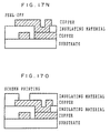
- an insulating material is coated by screen printing as shown in Fig. 17O.
- hole portions are formed in advance in the screen printing. Solder is adhered within these hole portions, and electronic parts or the like are made continuous via the soldering.
- devices are provided separately for the process of coating a conductive material or an insulating material on the medium on which writing is carried out, and the process of exposing the photoresist.
- the medium on which writing is carried out is set on stages provided at the respective devices, and the respective processes are carried out.
- the medium on which writing is carried out must be set at a stage each time a process is to be carried out, and much time is required for the operation.
- a silver salt photosensitive material which forms different colors when exposed at three wavelengths (e.g., R, G, B)
- black is exposed by UV (405 nm)
- red is exposed by B (450 nm) and G (532 nm)
- green is exposed by B (450 nm) and R (635 nm)
- blue is exposed by G (532 nm) and R (635 nm) by using an exposure device having four exposure heads (R, G, B, UV).
- the photosensitive material passes through a developing liquid and is developed, in the case in which the photosensitive material is a web, all of the colors are formed simultaneously, and patterns of the respective colors are formed.
- the thickness of the photosensitive material must be several tens of ⁇ m, and the accuracy of pattern formation has been insufficient.
- an object of the present invention is to provide a writing device which enables writing in two dimensions or three dimensions by a simple process and which enables highly-accurate pattern formation, and to provide a writing method using the writing device.
- a writing device carrying out writing of a multi-layer circuit pattern or the like on a medium on which writing is carried out, the writing device comprising: at least one exposure head and/or at least one discharging head; and a moving device which moves, relatively and in a predetermined direction, the heads and the medium on which writing is carried out, wherein the heads are disposed substantially parallel to the predetermined direction.
- a writing method which is used in a writing device which has at least one exposure head and/or at least one discharging head, the heads being disposed substantially parallel to a predetermined direction, the method comprising the steps of: providing a medium on which writing is carried out; moving, relatively and in a predetermined direction, the heads and the medium on which writing is carried out; as the relative movement is carried out, discharging a functional material from one of the discharging heads onto the medium on which writing is carried out; and carrying out exposure.
- a substantially parallelepiped scanning stage 12 is provided at a writing device 10.
- a printed board 14 serving as a medium on which writing is carried out is placed on the top surface of the scanning stage 12 in a positioned state.
- a substantially parallelepiped head holding body 16 is provided at the writing device 10 at an end portion along the longitudinal direction of the scanning stage 12.
- a guide rail 18 is disposed at the head holding body 16 along the longitudinal direction of the head holding body 16.
- An exposure head 20 and a discharging head 22 are supported in a cantilevered manner by connecting portions 26, 28, respectively, in a state of being orthogonal to the longitudinal direction of the head holding body 16.
- a discharging head 24 shown in Fig. 1 has substantially the same structure as the discharging head 22. Thus, illustration and description of the discharging head 24 will be omitted.
- the exposure head 20 and the discharging head 22 are movable in the direction of arrow A along the guide rail 18. (Hereinafter, the direction of arrow A will be called the "main scanning direction".)
- the connecting portions 26, 28 of the exposure head 20 and the discharging head 22 are linear motors (not shown). Due to the linear motors being driven by an unillustrated driving device, the exposure head 20 and the discharging head 22 move along the guide rail 18 via the connecting portions 26, 28.
- the control section of the writing device 10 has a CPU (central processing unit) 30.
- a CPU central processing unit 30.
- control such as the level of the laser energy and the like
- the set value of the level of the laser energy or the like which is suited to the operational conditions is read from a table 32 which is stored in a memory connected to the CPU 30 and in which is recorded the relationship between the head feeding speed and the recording conditions.
- a control signal which is for controlling the exposure head 20 on the basis of the set value of the level of the laser energy or the like which was read from the table 32, is transmitted to a recording condition setting circuit 34.
- the recording condition setting circuit 34 transmits a control signal, which includes the set value relating to the laser energy, to a recording laser driver 36.
- Laser light can be emitted due to the recording condition setting circuit 34 driving a fiber array light source 66 (see Figs. 4A and 4B) of the exposure head 20 via the recording laser driver 36.
- the CPU 30 transmits, to a main scanning driver 38 for the exposure head 20, a control signal for controlling the exposure head 20 on the basis of the set value of the level of the laser energy or the like which was read from the table 32.
- the main scanning driver 38 for the exposure head 20 transmits, to a driving device provided at the head holding body 16, a control signal for moving the exposure head 20, and makes the exposure head 20 move in the main scanning direction.
- the main scanning driver 38 for the exposure head 20 transmits a control signal to a recording synchronizing signal generating circuit 40, and transmits a synchronizing signal to a modulating element driver 42 via the recording synchronizing signal generating circuit 40 in order to synchronize the exposure timing of the exposure head 20 in accordance with the moving speed of the exposure head 20.
- recording information of a write pattern is read from recording data 44 stored in the memory of the CPU 30.
- the printed board 14 is exposed on the basis of the recording information of the write pattern.
- the CPU 30 transmits, to a main scanning driver 48 for the discharging head 22, a control signal for controlling the discharging head 22 on the basis of the set value of the level of the laser energy or the like which was read from the table 32.
- the main scanning driver 48 for the discharging head 22 transmits a control signal to the driving device which moves the discharging head 22, and makes the discharging head 22 move in the main scanning direction.
- the main scanning driver 48 for the discharging head 22 transmits, by an unillustrated synchronizing signal generating circuit, a synchronizing signal to a discharging element driver 50 in order to synchronize the timing for discharging a functional material filled in the discharging head 22 in accordance with the moving speed of the discharging head 22.
- the main scanning driver 48 for the discharging head 22 makes the functional material be discharged out onto the printed board 14 on the basis of the recording information of the recorded write pattern, by a discharging means which is an electrostatic type or the like.
- the CPU 30 transmits, to the driving device for moving the discharging head 24 and via a main scanning driver 52 for the discharging head 24, a control signal for controlling the discharging head 24 on the basis of the set level of the laser energy or the like which was read from the table 32, so as to make the discharging head 24 move in the main scanning direction.
- the CPU 30 transmits a synchronizing signal to a discharging element driver 54 via an unillustrated synchronizing signal generating circuit.
- the CPU 30 makes a functional material be discharged out onto the printed board 14 on the basis of the recording information of the recorded write pattern, by a discharging means which is an electrostatic type or the like.
- a screw portion (not shown) is provided at each of the connecting portions 26, 28 which connect the exposure head 20 and the discharging heads 22, 24 so as to be movable along the guide rail 18.
- the positions of the connecting portions 26, 28 with respect to the guide rail 18 can be adjusted in the direction of arrow A and in the direction of arrow B which is orthogonal to the direction of arrow A.
- the positions of the exposure head 20 and the discharging heads 22, 24 can be adjusted with respect to the direction of arrow A and the direction of arrow B.
- a prescribed pattern is patterned on the printed board 14 by the exposure head 20 and the discharging heads 22, 24, and the difference between a target pattern and the actual pattern is measured, and position adjustment is carried out.
- a pattern in which three discharging lines of the discharging head 22 coincide with the exposure line of the exposure head 20 is used as the target pattern. It is observed which of the discharging lines the exposure line corresponds to, and adjustment of the position of the exposure head 20 is carried out. Conversely, the position of the discharging head 22 may be adjusted by using the exposure line as a reference.
- positional adjustment of the exposure head 20 and the discharging heads 22, 24 can be carried out by the screw portions provided at the connecting portions 26, 28.
- arrangement data of the modulating elements used at the exposure head 20 or the discharging elements used at the discharging heads 22, 24 may be transmitted to an unillustrated control section, and the positions of the exposure head 20 and the discharging heads 22, 24 may be adjusted automatically.
- positional adjustment of the arrow A direction positions of the exposure line and the discharging lines can be carried out by adjusting the timing of the discharging or the exposure by the synchronizing signal generating circuits.
- the discharging heads 22, 24 are structured by an ink discharging system.
- the discharging heads 22, 24 are each structured by an electrostatic system, and discharge the functional materials filled therein by static electricity to the exterior.
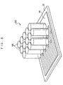
- the exposure head 20 is formed by a plurality of irradiating heads 56.
- a fiber array light source 66 is provided at each irradiating head 56.
- the light source wavelength is 350 to 450 nm. (However, in the heat mode, the range of wavelengths is broadened, and becomes 350 to 950 nm.)
- the laser light irradiated from the fiber array light source 66 is made into parallel light by a pair of combination lenses 71 forming a lens system 67.
- the parallel light is made incident on a pair of combination lenses 73.
- the combination lenses 73 have the following functions: with respect to the direction in which the laser emitting ends are arranged, the portions of the combination lenses 73 which are near to the optical axis of the lenses make the bundle of light widen, and the portions which are farther from the optical axis make the bundle of light contract, whereas with respect to the direction orthogonal to the direction in which the laser emitting ends are arranged, the combination lenses 73 transmit the light therethrough as is.
- the combination lenses 73 correct the laser light such that the light amount distribution thereof becomes uniform.
- the laser light whose light amount distribution has been corrected to be uniform by the combination lenses 73, is converged by a condensing lens 75. Via a reflecting mirror 69, the light is made incident on a digital micromirror device 68 (hereinafter, "DMD 68") which serves as a spatial light modulator which modulates the incident light beam for each pixel in accordance with image data.
- DMD 68 digital micromirror device 68
- the laser light which is incident on the DMD 68 is imaged on the printed board 14 by a lens system 70, 72.
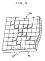
- the DMD 68 is a mirror device in which micromirrors 76 are supported by supports on an SRAM cell (memory cell) 74, and a large number (e.g., 600 ⁇ 800) micromirrors forming pixels are arrayed in a lattice form.
- the micromirror 76 supported at the uppermost portion of the support is provided for each pixel.
- a material having high reflectance such as aluminum or the like is deposited on the surface of the micromirror 76, such that the reflectance of the micromirror 76 is 90% or more.
- the SRAM cell 74 of a CMOS of a silicon gate which is fabricated on a usual semiconductor memory production line, is disposed directly beneath the micromirrors 76 via the supports which each include a hinge and a yoke. A monolithic structure is formed on the whole.
- the micromirrors 76 which are supported on the supports are tilted within a range of ⁇ ⁇ ° (e.g., ⁇ 10°) with respect to the substrate on which the DMD 68 is disposed and around a diagonal line.
- Fig. 6A shows a state in which the micromirror 76 is tilted by + ⁇ ° which is the on state.
- Figs. 6B shows a state in which the micromirror 76 is tilted by - ⁇ ° which is the off state.
- Fig. 5 is a view in which one portion of the DMD 68 is enlarged, and shows an example of a state in which the micromirrors 76 are controlled to + ⁇ ° or - ⁇ °.
- the on/off control of each micromirror 76 is carried out by an unillustrated controller connected to the DMD 68.
- a light absorbing body (not illustrated) is disposed in the direction in which the light beams are reflected by the micromirrors 76 which are in the off state.
- a large number (e.g., 800 columns ⁇ 600 rows) of the micromirrors 76 are arranged at the DMD 68.
- the DMDs 68 are disposed in a staggered form and are inclined slightly so as to form a predetermined angle (e.g., 0.1° to 5°) with respect to the main scanning direction (the direction of arrow A), and the exposure head 20 is main-scanned, adjacent exposed portions overlap slightly.
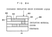
- an insulating resin dispersed liquid 80 is discharged onto the printed board 14, which is positioned on the top surface of the scanning stage 12 (see Fig. 1), by the insulating material discharging head 24 (see Fig. 1) on the basis of the recording information of the recorded write pattern.
- a copper particulate resin capsule dispersed liquid 82 serving as a conductive material is discharged on the basis of the recording information of the recorded write pattern, by the conductive material discharging head 22 (see Fig. 1) in which is filled a conductive material which exhibits electrical conductivity upon heating.
- the insulating resin dispersed liquid 80 may be discharged after the copper particulate resin capsule dispersed liquid 82 is discharged on the printed board 14.
- the entire surface of the printed board 14 is exposed by the exposure head 20 (see Fig. 1) having a heating function.
- the copper particulate resin capsule dispersed liquid 82 and the insulating resin dispersed liquid 80 are thereby hardened.
- the micromirrors 76 (see Fig. 5) of the DMD 68 (see Fig. 5) forming the exposure head 20 may be controlled so as to expose only the regions where the copper particulate resin capsule dispersed liquid 82 has been discharged. (Note that it is possible to carry out local exposure only at the necessary regions, and it is possible to expose a region which is slightly wider than the region where the copper particulate resin capsule dispersed liquid 82 has been discharged.)
- the printed board 14 can be exposed locally, and only the surface thereof is heated, which is different than in the case of thermoannealing.
- thermal expansion/contraction of the printed board 14 is avoided, and the heat-resistant temperature of the printed board 14 can be lowered.
- the time can be shortened as compared with a case in which thermoannealing is carried out.
- thermoannealing there is the problem that the resistance value cannot be sufficiently lowered (resistance value: 5 to 8 ⁇ 10 -5 ⁇ cm) because the resin within the copper particulate resin capsule dispersed liquid 82 does not completely transpire or because gaps remain between the copper particulates.
- resistance value 5 to 8 ⁇ 10 -5 ⁇ cm
- laser annealing there are resistance values (3 to 5 ⁇ 10 -6 ⁇ cm) which are equivalent to those of a copper wiring pattern formed by usual plating. Therefore, laser annealing can be widely used in general circuit board applications.
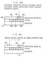
- the insulating resin dispersed liquid 80 is discharged by the insulating material discharging head 24 and the copper particulate resin capsule dispersed liquid 82 is discharged by the conductive material discharging head 22, onto an insulating layer 84 and a copper particulate layer 86 which have been formed by the copper particulate resin capsule dispersed liquid 82 and the insulating resin dispersed liquid 80 hardening.
- the entire printed board 14 is exposed by the exposure head 20, and the copper particulate resin capsule dispersed liquid 82 and the insulating material resin dispersed liquid 80 are hardened.
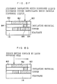
- the insulating resin dispersed liquid 80 is discharged by the insulating material discharging head 24 and the copper particulate resin capsule dispersed liquid 82 is discharged by the conductive material discharging head 22, onto the insulating layer 84 and the copper particulate layer 86.
- the entire surface of the printed board 14 is exposed by the exposure head 20, and the copper particulate resin capsule dispersed liquid 82 and the insulating resin dispersed liquid 80 are hardened.
- the insulating material resin dispersed liquid 80 is discharged by the insulating material discharging head 24 onto the insulating layer 84 and the copper particulate layer 86 such that the surface of the printed board 14 is covered by the insulating resin, except for the regions where solder is to be applied and the electrodes are to be led out from an external circuit board.
- a material which exhibits electrical conductivity by heating is discharged onto the printed board 14 by the discharging head 22 (a so-called coated state in which the material is discharged onto the entire surface of the printed board 14 may be used). Thereafter, by carrying out annealing (on the entire surface or locally) by the exposure head having a heating function, conductive patterning can be carried out easily, and a multi-layer circuit board 88 can be formed easily.
- the processes can be simplified, the time between patternings can be shortened, and pattern formation can be made to be more rapid, as compared with a case in which a scanning stage is provided for each head.
- pattern formation can be carried out even in the case of a mechanism in which there is very little leeway of time between patternings, e.g., a case in which the functional material such as an insulating material or a conductive material or the like is discharged, and thereafter, must be hardened before it deforms. Moreover, it is possible to harden the functional material before the functional material flows, and a highly-precise pattern is formed.
- the exposure head 20 and the discharging heads 22, 24 are placed on the same scanning stage, as compared with a case in which a scanning stage is provided for each head, the space required for placement of the entire device needed for forming the circuit pattern can be reduced, and costs and the amount of consumed electric power as well can be reduced.
- the exposure head 20 for annealing using a DMD as a light modulating device the electrostatic type discharging head 22 discharging the copper particulate resin capsule dispersed liquid 82, and the electrostatic type discharging head 24 discharging the insulating resin dispersed liquid 80, are provided at the scanning stage 12.
- the present invention is not limited to this embodiment.
- the irradiating head equipped with the DMD was described as the light modulating device of the exposure head.
- an MEMS (micro electro mechanical system) type spatial light modulator (SLM) or a spatial light modulator other than a MEMS type spatial light modulator such as an optical element modulating transmitted light by an electrooptical effect (a PLZT element), a liquid crystal light shutter (FLC) or the like is used
- the modulating speed per pixel and per scan line can be made faster by using some of the pixel portions as opposed to all of the pixel portions arrayed on the substrate.
- the same effects can be achieved.
- MEMS is a generic name for microsized sensors formed by a micro-machining technique based on an IC manufacturing process, actuators, and fine systems in which control circuits are integrated.
- a MEMS type spatial light modulator means a spatial light modulator which is driven by electromechanical action using static electricity.
- examples of the photosensitive material are photoresists, diazos, photopolymers, particulate dispersed materials (resins, dielectrics, conductive materials, and capsule-structured particles thereof), heat crystallized materials, heat-sensitive materials, heat transfer materials, molecule diffused materials (so-called sublimating-type heat transfer materials), and the like.
- examples of the form of the photosensitive material are film, liquid, solid, particulate, particulate dispersed liquid, particulate film-forming film (substrate) and the like.
- patterning an etching mask, a plating mask, water-repellant/hydrophilic, indentations and recesses, heat annealing, heat transfer, heat reaction, ablation, and the like
- a solid form formed by photo-curing, powder sintering, heat melting, or thermosetting to be formed as three-dimensional writing (a structure in which two-dimensional writing is repeated plural times).
- Examples of the ink jet head forming the discharging head are the on-demand nozzle type (piezo, electrostatic membrane, thermal, and the like), the continuous type (electric field deflection, heat deflection, or the like), and the on-demand nozzleless type (ultrasonic, electrostatic discharging, and the like).
- discharged material examples include photoreactive liquids, particulate dispersed liquids (resins, dielectrics, conductive bodies, heat crystallized materials, heat-sensitive materials, heat melting materials, molecule diffused materials (so-called sublimating-type heat transfer materials), catalysts, yeast, bacteria, DNA, chemically reactive chemicals, and the like, as well as capsule-structured particles thereof), heat melting liquids (wax and the like), chemically reactive liquids, catalyst solutions, surface modifying liquids, and the like.
- particulate dispersed liquids resins, dielectrics, conductive bodies, heat crystallized materials, heat-sensitive materials, heat melting materials, molecule diffused materials (so-called sublimating-type heat transfer materials), catalysts, yeast, bacteria, DNA, chemically reactive chemicals, and the like, as well as capsule-structured particles thereof
- heat melting liquids wax and the like
- chemically reactive liquids catalyst solutions, surface modifying liquids, and the like.
- a conductive particulate containing liquid discharging head and an exposure head may be used.
- a liquid 92 containing conductive particulates is discharged on the entire surface of a glass substrate 90 by a conductive particulate containing liquid discharging head.
- an insulating material which is coated by a liquid containing conductive particles, is annealed in a necessary conductive pattern form by the exposure head. In this way, a pattern 96 of a conductive film is formed, and a circuit board 98 is formed.
- particulates in which particulates of copper, silver, gold or the like which are 10 nm to 10 ⁇ m are covered by an insulating material, can be used as the conductive particulates.
- an insulating film discharging head and a circuit cutting pulse laser exposure head may be used.
- a transparent insulating film is discharged on the entire surface of a conductive film 102 which is the outermost layer of a printed board 100 by an insulating film discharging head.
- This transparent insulating film is exposed by an exposure head having a wavelength which can pass through the transparent insulating film but is absorbed by a conductive film formed by plating or a conductive film discharging head.
- a circuit board 103 in which the circuit pattern of the conductive film 102 is cut and a cavity is formed, is formed.
- circuit board 103 it is possible to change the circuit pattern which does not appear at the surface, and the circuit pattern can be heated in a state in which it is not contacting air. Therefore, it is difficult for the conductive film material at the periphery of the cut portion to oxidize.
- an insulating film discharging head by using an insulating film discharging head, a marking ink discharging head, or a pulse laser marking exposure head, formation of a mark such as a number, a bar code, an alignment mark or the like can be carried out by the exposure head or the discharging head before the insulating film of the outermost layer is formed.
- a mark is formed before the insulating film of the outermost layer is formed, the mark is not directly exposed at the surface, and it is possible to prevent the mark from being illicitly tampered with or from being removed. Moreover, because each layer can be marked with different contents, it is possible to prevent mistakes in the inspection conditions when the circuit is different at each layer, and it is possible to prevent mistakes in packaging when the circuit board is packaged in a final product.
- a spacer structuring material discharging head and a laser exposure head for hardening may be used.
- spacers 106 for making the glass intervals of an LCD 104 uniform are discharged by the spacer structuring material discharging head.
- Fig. 11B only the peripheries of corresponding positions of the spacers 106 are irradiated by the exposure head (if the material is a photo-curing type material, an ultraviolet laser of 350 to 450 nm is used as the light source, and if the material is a thermosetting type material, a high power laser of 350 to 950 nm is used as the light source), such that the spacers 106 are hardened.
- a substrate 105 is thereby formed.
- the precision of the heights of the spacers 106 is improved, and the strength of the spacers 106 also can be improved.
- the present invention can also be applied to spacers for bumps of wafer level flip-chips.
- a photopolymer discharging head and an exposure head for hardening may be used.
- a photopolymer is discharged in the form of a pattern of one layer, by the photopolymer discharging head on the top surface of a stand 110 which is provided so as to be able to be raised and lowered.
- Fig. 12B light of 350 to 450 nm is irradiated by the exposure head and the photopolymer is hardened.
- the stand 110 is lowered (about 50 ⁇ m), and the photopolymer discharging head and the exposure head for hardening are raised relatively by an amount corresponding to one layer. At this time, the exposure head and the photopolymer discharging head are returned to reference positions.
- a photopolymer is discharged in the form of a pattern of one layer by the photopolymer discharging head. Thereafter, the photopolymer is hardened by the exposure head.
- the stand 110 is lowered, and the photopolymer discharging head and the exposure head for hardening are raised relatively by an amount corresponding to one layer.
- a circuit board 112 is formed. As compared with a structure which cannot be hardened by light, it is possible to carry out high-strength and highly accurate formation of a solid.
- a conductive material discharging head and a pulse laser exposure head for trimming may be used.
- a conductive circuit conductive material
- a pulse laser exposure head for trimming.
- a conductive circuit conductive material
- a pulse laser exposure head for trimming.
- a circuit board 115 is formed.
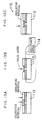
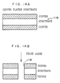
- an exposure head for a photoresist and a pulse laser exposure head for through holes may be used.
- a through hole 118 is formed by the pulse laser exposure head for through holes, which is mounted to a pulse laser, in a copper plated substrate which has been copper plated as shown in Fig. 14A.
- both surfaces of the copper plated substrate 116 are laminated by a film-shaped photoresist.
- the photoresists are hardened by the exposure head for the photoresist.
- the portions of the photoresist which were not exposed by developing are removed.
- a so-called negative type photoresist is used which becomes insoluble in a developing liquid by exposure.
- a so-called positive type photoresist which can dissolve easily in a developing liquid by exposure. In cases in which a positive type photoresist is used, the portions of the photoresist exposed by developing are removed.
- the photoresist is removed, and the exposed copper is etched by etching.
- Fig. 14F the photoresist is peeled off.
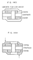
- Fig. 14G both surfaces of the copper plated substrate 116 are laminated by a film-shaped photoresist.
- Fig. 14H the photoresists are hardened by the exposure head for a photoresist.
- Fig. 14I the portions of the photoresist which were not exposed by developing are removed.
- the inner edge portion of the through hole 118 formed in the copper plated substrate 116 is plated.
- the photoresist is peeled off, and a circuit board 120 is formed.
- a pattern is formed in a state in which the printed board is placed on the scanning stage.
- a pattern may be formed by fixing the respective heads and moving the medium on which writing is carried out.
- an elongated web 122 is used as the medium on which writing is carried out.
- the web 122 which is fed out by a feed-out device 124 is taken-up by a take-up device 126.
- a conveying path 128 is formed between the feed-out device 124 and the take-up device 126.
- photoresist discharging heads 130 which discharge a photoresist
- exposure heads 132 developing liquid discharging heads 134 which discharge developing liquid
- etching liquid discharging heads 138 which discharge etching liquid
- rinsing liquid discharging heads 140 which discharge rinsing liquid
- the respective heads are disposed above and below the web 122 which is being conveyed. However, it is possible to provide the respective heads either only above or only below the web 122. Further, here, the developing liquid discharging heads 134, the etching liquid discharging heads 138, and the rinsing liquid discharging heads 140 are used. However, it is not absolutely necessary to employ discharging heads, and tanks holding the developing liquid, the etching liquid, and the rinsing liquid, respectively, may be used.
- an exposure head 142 and discharging heads 144, 146 may be serial heads.
- discharging heads are serial heads and the exposure head is a line head
- discharging heads are line heads and the exposure head is a polygon scanning head
- discharging heads are line heads and the exposure head is a serial head, and the like.
- the present invention has the above-described structure, due to a circuit pattern being formed on a medium on which writing is carried out on a same scanning stage, positional offset of respective heads with respect to the medium on which writing is carried out does not arise. Thus, it is easy to make the pattern highly precise.
- the respective heads at the same scanning stage, as compared with a case in which a scanning stage is provided for each head, the space required for placement of the entire device needed for forming the circuit pattern can be reduced. Moreover, costs and the amount of electricity which is consumed can be reduced.
Landscapes
- Engineering & Computer Science (AREA)
- Manufacturing & Machinery (AREA)
- Microelectronics & Electronic Packaging (AREA)
- Physics & Mathematics (AREA)
- General Physics & Mathematics (AREA)
- Exposure And Positioning Against Photoresist Photosensitive Materials (AREA)
- Manufacturing Of Printed Circuit Boards (AREA)
- Manufacturing Of Printed Wiring (AREA)
Applications Claiming Priority (3)
| Application Number | Priority Date | Filing Date | Title |
|---|---|---|---|
| JP2002167409A JP2004012902A (ja) | 2002-06-07 | 2002-06-07 | 描画装置及びこの描画装置を用いた描画方法 |
| JP2002167409 | 2002-06-07 | ||
| PCT/JP2003/007195 WO2003105547A1 (fr) | 2002-06-07 | 2003-06-06 | Dispositif de trace et procede de trace |
Publications (2)
| Publication Number | Publication Date |
|---|---|
| EP1513380A1 true EP1513380A1 (fr) | 2005-03-09 |
| EP1513380A4 EP1513380A4 (fr) | 2008-01-16 |
Family
ID=29706761
Family Applications (1)
| Application Number | Title | Priority Date | Filing Date |
|---|---|---|---|
| EP03736076A Withdrawn EP1513380A4 (fr) | 2002-06-07 | 2003-06-06 | Dispositif de trace et procede de trace |
Country Status (7)
| Country | Link |
|---|---|
| US (1) | US7014986B2 (fr) |
| EP (1) | EP1513380A4 (fr) |
| JP (1) | JP2004012902A (fr) |
| KR (1) | KR100661343B1 (fr) |
| CN (1) | CN1659937A (fr) |
| TW (1) | TWI222313B (fr) |
| WO (1) | WO2003105547A1 (fr) |
Cited By (1)
| Publication number | Priority date | Publication date | Assignee | Title |
|---|---|---|---|---|
| CN102681355A (zh) * | 2011-03-18 | 2012-09-19 | 大日本网屏制造株式会社 | 描画数据修正装置及描画装置 |
Families Citing this family (14)
| Publication number | Priority date | Publication date | Assignee | Title |
|---|---|---|---|---|
| JP4630542B2 (ja) * | 2003-12-22 | 2011-02-09 | キヤノン株式会社 | 配線形成方法 |
| CN1899004A (zh) * | 2003-12-22 | 2007-01-17 | 佳能株式会社 | 布线形成方法、布线形成装置以及布线板 |
| US7354845B2 (en) * | 2004-08-24 | 2008-04-08 | Otb Group B.V. | In-line process for making thin film electronic devices |
| NL1026013C2 (nl) * | 2004-04-23 | 2005-10-25 | Otb Group Bv | Werkwijze en inrichting voor het nauwkeurig aanbrengen van structuren op een substraat. |
| JP4715147B2 (ja) * | 2004-09-28 | 2011-07-06 | セイコーエプソン株式会社 | 導電膜の形成方法 |
| JP4580799B2 (ja) * | 2005-03-29 | 2010-11-17 | 大日本印刷株式会社 | 導電性可変組成物、導電性可変積層体、導電性パターン形成体および有機エレクトロルミネッセント素子 |
| US8147903B2 (en) * | 2005-06-22 | 2012-04-03 | Canon Kabushiki Kaisha | Circuit pattern forming method, circuit pattern forming device and printed circuit board |
| JP2007033764A (ja) * | 2005-07-26 | 2007-02-08 | Fujifilm Holdings Corp | パターン製造システム、露光装置、及び露光方法 |
| JP4914589B2 (ja) | 2005-08-26 | 2012-04-11 | 三菱電機株式会社 | 半導体製造装置、半導体製造方法および半導体装置 |
| JP2007093646A (ja) * | 2005-09-27 | 2007-04-12 | Sumitomo Heavy Ind Ltd | 直接描画装置 |
| US20120330234A1 (en) * | 2010-03-16 | 2012-12-27 | Barkey Gmbh & Co. Kg | Device for heating flowing fluids and production method |
| US9482963B2 (en) | 2010-12-20 | 2016-11-01 | Asml Netherlands B.V. | Method of controlling a patterning device in a lithographic apparatus, device manufacturing method and lithographic apparatus |
| CN110605917B (zh) * | 2019-08-29 | 2021-03-16 | 深圳市汉森软件有限公司 | 用于pcb字符的打印控制方法、装置、设备及存储介质 |
| CN114911135B (zh) * | 2021-02-09 | 2025-09-12 | 源能智创(江苏)半导体有限公司 | 一种防焊油墨的曝光方法 |
Family Cites Families (14)
| Publication number | Priority date | Publication date | Assignee | Title |
|---|---|---|---|---|
| US5594652A (en) * | 1991-01-31 | 1997-01-14 | Texas Instruments Incorporated | Method and apparatus for the computer-controlled manufacture of three-dimensional objects from computer data |
| JP3564735B2 (ja) * | 1994-06-16 | 2004-09-15 | 株式会社ニコン | 走査型露光装置及び露光方法 |
| JPH10112579A (ja) * | 1996-10-07 | 1998-04-28 | M S Tec:Kk | レジスト露光方法及びその露光装置 |
| JP3037158B2 (ja) | 1996-10-07 | 2000-04-24 | ユーエイチティー株式会社 | プリント配線体の製造方法並びにその製造装置 |
| JPH11163499A (ja) | 1997-11-28 | 1999-06-18 | Nitto Boseki Co Ltd | プリント配線板の製造方法及びこの製造方法によるプリント配線板 |
| JPH11253860A (ja) | 1998-03-12 | 1999-09-21 | Canon Inc | パターン形成装置および方法 |
| JP4741045B2 (ja) * | 1998-03-25 | 2011-08-03 | セイコーエプソン株式会社 | 電気回路、その製造方法および電気回路製造装置 |
| GB2350321A (en) * | 1999-05-27 | 2000-11-29 | Patterning Technologies Ltd | Method of forming a masking or spacer pattern on a substrate using inkjet droplet deposition |
| JP3587442B2 (ja) | 1999-08-19 | 2004-11-10 | 大日本スクリーン製造株式会社 | レーザプロッタ |
| JP2001125274A (ja) * | 1999-10-26 | 2001-05-11 | Matsushita Electric Works Ltd | 回路板製造用露光装置 |
| JP2002158394A (ja) * | 2000-11-17 | 2002-05-31 | Fuji Photo Film Co Ltd | 露光ヘッドおよび画像記録装置 |
| JP4210038B2 (ja) * | 2001-03-02 | 2009-01-14 | 富士フイルム株式会社 | 画像転写記録装置 |
| CN1659479A (zh) * | 2002-04-10 | 2005-08-24 | 富士胶片株式会社 | 曝光头及曝光装置和它的应用 |
| JP4201178B2 (ja) * | 2002-05-30 | 2008-12-24 | 大日本スクリーン製造株式会社 | 画像記録装置 |
-
2002
- 2002-06-07 JP JP2002167409A patent/JP2004012902A/ja active Pending
-
2003
- 2003-06-05 TW TW092115172A patent/TWI222313B/zh not_active IP Right Cessation
- 2003-06-06 US US10/455,403 patent/US7014986B2/en not_active Expired - Lifetime
- 2003-06-06 EP EP03736076A patent/EP1513380A4/fr not_active Withdrawn
- 2003-06-06 WO PCT/JP2003/007195 patent/WO2003105547A1/fr not_active Ceased
- 2003-06-06 CN CN038131935A patent/CN1659937A/zh active Pending
- 2003-06-06 KR KR1020047019930A patent/KR100661343B1/ko not_active Expired - Lifetime
Cited By (2)
| Publication number | Priority date | Publication date | Assignee | Title |
|---|---|---|---|---|
| CN102681355A (zh) * | 2011-03-18 | 2012-09-19 | 大日本网屏制造株式会社 | 描画数据修正装置及描画装置 |
| CN102681355B (zh) * | 2011-03-18 | 2014-08-13 | 大日本网屏制造株式会社 | 描画数据修正装置及描画装置 |
Also Published As
| Publication number | Publication date |
|---|---|
| US20030228543A1 (en) | 2003-12-11 |
| TWI222313B (en) | 2004-10-11 |
| JP2004012902A (ja) | 2004-01-15 |
| EP1513380A4 (fr) | 2008-01-16 |
| WO2003105547A1 (fr) | 2003-12-18 |
| KR20050008806A (ko) | 2005-01-21 |
| KR100661343B1 (ko) | 2006-12-27 |
| CN1659937A (zh) | 2005-08-24 |
| US7014986B2 (en) | 2006-03-21 |
| TW200404451A (en) | 2004-03-16 |
Similar Documents
| Publication | Publication Date | Title |
|---|---|---|
| US7014986B2 (en) | Writing device and writing method | |
| US6832045B2 (en) | Exposure device | |
| Jain et al. | Flexible electronics and displays: high-resolution, roll-to-roll, projection lithography and photoablation processing technologies for high-throughput production | |
| US9645502B2 (en) | Lithographic apparatus, programmable patterning device and lithographic method | |
| KR101616761B1 (ko) | 리소그래피 장치, 프로그램가능한 패터닝 디바이스 및 리소그래피 방법 | |
| US5330878A (en) | Method and apparatus for patterning an imaging member | |
| US7212327B2 (en) | Imaging head, imaging device and imaging method | |
| EP2109350B1 (fr) | Système pour la création de lignes fines avec la technologie de jet d'encre | |
| JPH0653105A (ja) | 露光装置 | |
| KR20180100168A (ko) | 직접 기입 마스크리스 리소그래피를 위한 방법 및 장치 | |
| US7197201B2 (en) | Optical wiring substrate fabrication process and optical wiring substrate device | |
| CN105659165A (zh) | 光刻设备、图案形成装置和光刻方法 | |
| CN108605413A (zh) | 用于在二维的、快速退火的环境中直接曝光止焊漆的直接曝光装置 | |
| KR20160073416A (ko) | 포토레지스트 두께에 따라 라이팅 빔들의 전달 도즈를 변화시키기 위한 프로세서들을 이용하는 패턴 생성기들, 및 관련 방법들 | |
| TWI261456B (en) | Graphics plotting device and the method | |
| US20050157286A1 (en) | Method and system for detecting sensitivity of photosensitive materials and exposure correcting method | |
| US20050129397A1 (en) | Exposure device | |
| JP2001180038A (ja) | レーザマーキング方法及び同方法を実施するためのレーザマーカ | |
| JPS63166555A (ja) | サ−マルヘツドの製造方法 |
Legal Events
| Date | Code | Title | Description |
|---|---|---|---|
| PUAI | Public reference made under article 153(3) epc to a published international application that has entered the european phase |
Free format text: ORIGINAL CODE: 0009012 |
|
| 17P | Request for examination filed |
Effective date: 20041126 |
|
| AK | Designated contracting states |
Kind code of ref document: A1 Designated state(s): AT BE BG CH CY CZ DE DK EE ES FI FR GB GR HU IE IT LI LU MC NL PT RO SE SI SK TR |
|
| RBV | Designated contracting states (corrected) |
Designated state(s): DE FR |
|
| RAP1 | Party data changed (applicant data changed or rights of an application transferred) |
Owner name: FUJIFILM CORPORATION |
|
| A4 | Supplementary search report drawn up and despatched |
Effective date: 20071218 |
|
| RIC1 | Information provided on ipc code assigned before grant |
Ipc: H05K 3/10 20060101ALI20071213BHEP Ipc: G03F 7/16 20060101ALN20071213BHEP Ipc: G03F 7/20 20060101ALI20071213BHEP Ipc: H05K 3/46 20060101ALN20071213BHEP Ipc: H05K 3/00 20060101AFI20071213BHEP |
|
| STAA | Information on the status of an ep patent application or granted ep patent |
Free format text: STATUS: THE APPLICATION IS DEEMED TO BE WITHDRAWN |
|
| 18D | Application deemed to be withdrawn |
Effective date: 20080315 |