EP1511632B1 - Verfahren und vorrichtung zur übertragung eines musters von einem stempel auf ein substrat - Google Patents
Verfahren und vorrichtung zur übertragung eines musters von einem stempel auf ein substrat Download PDFInfo
- Publication number
- EP1511632B1 EP1511632B1 EP03727761A EP03727761A EP1511632B1 EP 1511632 B1 EP1511632 B1 EP 1511632B1 EP 03727761 A EP03727761 A EP 03727761A EP 03727761 A EP03727761 A EP 03727761A EP 1511632 B1 EP1511632 B1 EP 1511632B1
- Authority
- EP
- European Patent Office
- Prior art keywords
- stamp
- receiving surface
- stamping
- pattern
- stamping surface
- Prior art date
- Legal status (The legal status is an assumption and is not a legal conclusion. Google has not performed a legal analysis and makes no representation as to the accuracy of the status listed.)
- Expired - Lifetime
Links
- 239000000758 substrate Substances 0.000 title claims abstract description 71
- 238000000034 method Methods 0.000 title claims abstract description 54
- 238000012546 transfer Methods 0.000 claims abstract description 71
- 238000007639 printing Methods 0.000 claims description 83
- 238000002174 soft lithography Methods 0.000 claims description 8
- 230000008901 benefit Effects 0.000 description 27
- 239000012530 fluid Substances 0.000 description 20
- 230000009471 action Effects 0.000 description 17
- 238000003825 pressing Methods 0.000 description 12
- BQCADISMDOOEFD-UHFFFAOYSA-N Silver Chemical compound [Ag] BQCADISMDOOEFD-UHFFFAOYSA-N 0.000 description 10
- 239000000463 material Substances 0.000 description 10
- 230000008569 process Effects 0.000 description 10
- 229910052709 silver Inorganic materials 0.000 description 9
- 239000004332 silver Substances 0.000 description 9
- 238000005096 rolling process Methods 0.000 description 6
- 239000007788 liquid Substances 0.000 description 5
- 238000004519 manufacturing process Methods 0.000 description 5
- 239000011521 glass Substances 0.000 description 4
- 238000007689 inspection Methods 0.000 description 4
- BFXIKLCIZHOAAZ-UHFFFAOYSA-N methyltrimethoxysilane Chemical compound CO[Si](C)(OC)OC BFXIKLCIZHOAAZ-UHFFFAOYSA-N 0.000 description 4
- XLYOFNOQVPJJNP-UHFFFAOYSA-N water Substances O XLYOFNOQVPJJNP-UHFFFAOYSA-N 0.000 description 4
- XUIMIQQOPSSXEZ-UHFFFAOYSA-N Silicon Chemical compound [Si] XUIMIQQOPSSXEZ-UHFFFAOYSA-N 0.000 description 3
- 238000009792 diffusion process Methods 0.000 description 3
- 239000004205 dimethyl polysiloxane Substances 0.000 description 3
- 238000006073 displacement reaction Methods 0.000 description 3
- 239000002798 polar solvent Substances 0.000 description 3
- 229920000435 poly(dimethylsiloxane) Polymers 0.000 description 3
- 229910052710 silicon Inorganic materials 0.000 description 3
- 239000010703 silicon Substances 0.000 description 3
- 239000002904 solvent Substances 0.000 description 3
- QTBSBXVTEAMEQO-UHFFFAOYSA-N Acetic acid Chemical compound CC(O)=O QTBSBXVTEAMEQO-UHFFFAOYSA-N 0.000 description 2
- LFQSCWFLJHTTHZ-UHFFFAOYSA-N Ethanol Chemical compound CCO LFQSCWFLJHTTHZ-UHFFFAOYSA-N 0.000 description 2
- BOTDANWDWHJENH-UHFFFAOYSA-N Tetraethyl orthosilicate Chemical compound CCO[Si](OCC)(OCC)OCC BOTDANWDWHJENH-UHFFFAOYSA-N 0.000 description 2
- 230000008859 change Effects 0.000 description 2
- 238000013461 design Methods 0.000 description 2
- 239000006185 dispersion Substances 0.000 description 2
- 239000011888 foil Substances 0.000 description 2
- 238000010438 heat treatment Methods 0.000 description 2
- 229910052751 metal Inorganic materials 0.000 description 2
- 239000002184 metal Substances 0.000 description 2
- 238000000813 microcontact printing Methods 0.000 description 2
- 239000000203 mixture Substances 0.000 description 2
- 238000000206 photolithography Methods 0.000 description 2
- -1 polydimethylsiloxane Polymers 0.000 description 2
- 229920000642 polymer Polymers 0.000 description 2
- 239000004065 semiconductor Substances 0.000 description 2
- 230000007480 spreading Effects 0.000 description 2
- 238000003892 spreading Methods 0.000 description 2
- 235000012431 wafers Nutrition 0.000 description 2
- OKTJSMMVPCPJKN-UHFFFAOYSA-N Carbon Chemical compound [C] OKTJSMMVPCPJKN-UHFFFAOYSA-N 0.000 description 1
- 229910000608 Fe(NO3)3.9H2O Inorganic materials 0.000 description 1
- 238000005411 Van der Waals force Methods 0.000 description 1
- 229960000583 acetic acid Drugs 0.000 description 1
- 230000004913 activation Effects 0.000 description 1
- 239000012190 activator Substances 0.000 description 1
- 150000001298 alcohols Chemical class 0.000 description 1
- 239000002041 carbon nanotube Substances 0.000 description 1
- 229910021393 carbon nanotube Inorganic materials 0.000 description 1
- 230000000295 complement effect Effects 0.000 description 1
- 230000001419 dependent effect Effects 0.000 description 1
- 230000008020 evaporation Effects 0.000 description 1
- 238000001704 evaporation Methods 0.000 description 1
- 239000012362 glacial acetic acid Substances 0.000 description 1
- 238000007641 inkjet printing Methods 0.000 description 1
- 229910000765 intermetallic Inorganic materials 0.000 description 1
- MVFCKEFYUDZOCX-UHFFFAOYSA-N iron(2+);dinitrate Chemical compound [Fe+2].[O-][N+]([O-])=O.[O-][N+]([O-])=O MVFCKEFYUDZOCX-UHFFFAOYSA-N 0.000 description 1
- 238000012423 maintenance Methods 0.000 description 1
- 238000004377 microelectronic Methods 0.000 description 1
- 238000012986 modification Methods 0.000 description 1
- 230000004048 modification Effects 0.000 description 1
- 230000003287 optical effect Effects 0.000 description 1
- 239000011368 organic material Substances 0.000 description 1
- 150000002902 organometallic compounds Chemical class 0.000 description 1
- 238000000059 patterning Methods 0.000 description 1
- 229920002120 photoresistant polymer Polymers 0.000 description 1
- 238000005498 polishing Methods 0.000 description 1
- 229920002635 polyurethane Polymers 0.000 description 1
- 239000004814 polyurethane Substances 0.000 description 1
- 239000002243 precursor Substances 0.000 description 1
- 239000010453 quartz Substances 0.000 description 1
- 230000000630 rising effect Effects 0.000 description 1
- VYPSYNLAJGMNEJ-UHFFFAOYSA-N silicon dioxide Inorganic materials O=[Si]=O VYPSYNLAJGMNEJ-UHFFFAOYSA-N 0.000 description 1
- 238000003756 stirring Methods 0.000 description 1
- 230000002123 temporal effect Effects 0.000 description 1
- 239000010409 thin film Substances 0.000 description 1
- 230000001052 transient effect Effects 0.000 description 1
Images


Classifications
-
- B—PERFORMING OPERATIONS; TRANSPORTING
- B05—SPRAYING OR ATOMISING IN GENERAL; APPLYING FLUENT MATERIALS TO SURFACES, IN GENERAL
- B05C—APPARATUS FOR APPLYING FLUENT MATERIALS TO SURFACES, IN GENERAL
- B05C17/00—Hand tools or apparatus using hand held tools, for applying liquids or other fluent materials to, for spreading applied liquids or other fluent materials on, or for partially removing applied liquids or other fluent materials from, surfaces
- B05C17/06—Stencils
-
- G—PHYSICS
- G03—PHOTOGRAPHY; CINEMATOGRAPHY; ANALOGOUS TECHNIQUES USING WAVES OTHER THAN OPTICAL WAVES; ELECTROGRAPHY; HOLOGRAPHY
- G03F—PHOTOMECHANICAL PRODUCTION OF TEXTURED OR PATTERNED SURFACES, e.g. FOR PRINTING, FOR PROCESSING OF SEMICONDUCTOR DEVICES; MATERIALS THEREFOR; ORIGINALS THEREFOR; APPARATUS SPECIALLY ADAPTED THEREFOR
- G03F7/00—Photomechanical, e.g. photolithographic, production of textured or patterned surfaces, e.g. printing surfaces; Materials therefor, e.g. comprising photoresists; Apparatus specially adapted therefor
- G03F7/0002—Lithographic processes using patterning methods other than those involving the exposure to radiation, e.g. by stamping
-
- B—PERFORMING OPERATIONS; TRANSPORTING
- B05—SPRAYING OR ATOMISING IN GENERAL; APPLYING FLUENT MATERIALS TO SURFACES, IN GENERAL
- B05C—APPARATUS FOR APPLYING FLUENT MATERIALS TO SURFACES, IN GENERAL
- B05C1/00—Apparatus in which liquid or other fluent material is applied to the surface of the work by contact with a member carrying the liquid or other fluent material, e.g. a porous member loaded with a liquid to be applied as a coating
- B05C1/02—Apparatus in which liquid or other fluent material is applied to the surface of the work by contact with a member carrying the liquid or other fluent material, e.g. a porous member loaded with a liquid to be applied as a coating for applying liquid or other fluent material to separate articles
- B05C1/027—Apparatus in which liquid or other fluent material is applied to the surface of the work by contact with a member carrying the liquid or other fluent material, e.g. a porous member loaded with a liquid to be applied as a coating for applying liquid or other fluent material to separate articles only at particular parts of the articles
-
- B—PERFORMING OPERATIONS; TRANSPORTING
- B05—SPRAYING OR ATOMISING IN GENERAL; APPLYING FLUENT MATERIALS TO SURFACES, IN GENERAL
- B05D—PROCESSES FOR APPLYING FLUENT MATERIALS TO SURFACES, IN GENERAL
- B05D1/00—Processes for applying liquids or other fluent materials
- B05D1/28—Processes for applying liquids or other fluent materials performed by transfer from the surfaces of elements carrying the liquid or other fluent material, e.g. brushes, pads, rollers
-
- B—PERFORMING OPERATIONS; TRANSPORTING
- B05—SPRAYING OR ATOMISING IN GENERAL; APPLYING FLUENT MATERIALS TO SURFACES, IN GENERAL
- B05D—PROCESSES FOR APPLYING FLUENT MATERIALS TO SURFACES, IN GENERAL
- B05D1/00—Processes for applying liquids or other fluent materials
- B05D1/32—Processes for applying liquids or other fluent materials using means for protecting parts of a surface not to be coated, e.g. using stencils, resists
-
- B—PERFORMING OPERATIONS; TRANSPORTING
- B82—NANOTECHNOLOGY
- B82Y—SPECIFIC USES OR APPLICATIONS OF NANOSTRUCTURES; MEASUREMENT OR ANALYSIS OF NANOSTRUCTURES; MANUFACTURE OR TREATMENT OF NANOSTRUCTURES
- B82Y10/00—Nanotechnology for information processing, storage or transmission, e.g. quantum computing or single electron logic
-
- B—PERFORMING OPERATIONS; TRANSPORTING
- B82—NANOTECHNOLOGY
- B82Y—SPECIFIC USES OR APPLICATIONS OF NANOSTRUCTURES; MEASUREMENT OR ANALYSIS OF NANOSTRUCTURES; MANUFACTURE OR TREATMENT OF NANOSTRUCTURES
- B82Y40/00—Manufacture or treatment of nanostructures
Definitions
- the present invention relates to the field of soft lithographic printing, wherein the features of the pattern to be transferred are in the micron and submicron range.
- the first printing principle comprises pressing two sheets against each other, wherein the two sheets contact each other through a plane.
- An important advantage of this first printing principle is that the alignment of the two sheets with respect to each other can be performed very accurately. Further, after the sheets have been pressed together, they stick together as a result of Van der Waals forces and can not easily be separated.
- An important disadvantage of this printing principle is that on moving of the sheets towards each other, air may be entrapped between the sheets. As a result, the transfer of the pattern may be incomplete.
- WO 97/06012 discloses a hybrid stamp structure for lithographic processes of features below 1 micron.
- the hybrid stamp comprises a deformable layer for accommodating unevenness of the surface of a substrate and of the stamp structure itself, and a patterned layer in which a lithographic pattern is engraved.
- the stamp is further enhanced by a third layer which acts as rigid support for the stamp, thus preventing an undesired deformation of the stamp under load.
- the second printing principle comprises rolling of a cylinder along a sheet, wherein the cylinder and the sheet contact each other along a line.
- An important advantage of this printing principle is that air gets displaced on rolling of the cylinder, so that entrapment of air bubbles between the cylinder and the sheet will not occur, and the transfer of the pattern will not be interrupted. Also, the cylinder and the sheet do not stick together, contrary to two sheets.
- An important disadvantage of this second printing principle is that it is very difficult to align the cylinder and the sheet with respect to each other in an accurate way. Therefore, it is very difficult to reproduce the movement of the cylinder along the sheet two or more times, which is necessary in cases where the substrate needs to be provided with two or more layers.
- a flexible stamp is applied, which has a stamping surface including a pattern, wherein the stamping surface is flat in an unstressed condition.
- the flexible stamp is positioned above a support structure, such that the stamping surface opposes a surface of said support structure, and is secured along its circumference.
- an article is placed onto the surface of the support structure, such that a surface of the article opposes the stamping surface.
- Both the stamping surface and the article are within a pressure-controlled chamber filled with gas. Initially, the pressure in the chamber equals the pressure acting on a back surface of the flexible stamp, which is the atmospheric pressure.
- the stamping surface After the stamping surface is wetted with a fluid, the stamping surface is brought into contact with the surface of the article by reducing the pressure of the gas within the chamber.
- the process of reducing the pressure is performed in a controlled manner, so that contact between the stamping surface and the surface of the article commences at the center of the flexible stamp and proceeds outwardly away from the center.
- the stamping surface is controllably contacted with the surface of the article, so that the pattern of the stamping surface is stamped onto the surface of the article.
- the flexible stamp When the pressure in the chamber is reduced, a pressure differential is established across the flexible stamp. As a result, the flexible stamp bulges in the direction of the article, wherein the center of the flexible stamp contacts the article at first. After the entire pattern has been stamped onto the surface of the article, the flexible stamp is removed from the article by increasing the pressure of the gas within the chamber. The process of increasing the pressure is performed in a controlled manner, so that the flexible stamp peels off from the surface of the article without distorting the pattern of the layer of fluid.
- the known method combines the advantages of both the printing principle of rolling of a cylinder along a sheet and the printing principle of pressing two sheets against each other. Alignment of the stamp with respect to the article can be performed in an accurate manner, since the stamping surface is initially flat. Entrapment of air bubbles does not occur, since contact between the stamping surface and the surface of the article commences at the center of the flexible stamp and proceeds outwardly away from the center.
- the known method has an important drawback, which does not occur with one of the above-mentioned first and second printing principles.
- individual transfer areas are created between the stamping surface and the receiving surface by successively moving portions of at least one of the surfaces in a direction substantially perpendicular to the receiving surface.
- a different process takes place, wherein one transfer area is created which at first expands and later diminishes.
- Another advantage of the present invention is that during the transfer of the pattern no air bubbles will be entrapped between the stamping surface and the receiving surface, due to the fact that the portions are successively moved. Even in case of both the stamping surface and the receiving surface being substantially flat, air will not be present in the transfer areas, since air is allowed to be displaced during creation of the transfer areas.
- Yet another advantage of the present invention is that the pressing force can be controlled in an accurate manner.
- the present invention offers the possibility of individually controlling the pressing force for every portion of the pattern.
- first transfer period and the second transfer period partly overlap. This is advantageous in order to reduce the time needed for the transfer of the pattern. Further on, it may stabilize the transfer.
- first portion and the second portion are adjacent portions. This allows, in particular in combination with a partial overlap of the transfer periods, a printing procedure analogous to the flowing of a transversal wave.
- the pattern may be transferred according to various shapes.
- the second transfer area may be shaped like a ring, providing a circular propagation of the wavelike transfer.
- the first and second area are linear and are aligned parallel to each other.
- the shape is not limited to a wave.
- the individual portions or sets of individual portions transferred do not need to be neighboring.
- such allows the use of one stamp, of which dots can be printed as desired.
- the pattern of dots to be printed can be prescribed using known control device, particularly a computer comprising a control program with at least one desired pattern to be printed on the receiving surface.
- This leads to a printing type which is comparable to conventional desktop or inkjet printing, achieving a resolution of typically 1 ⁇ m currently. However this resolution may be further improved.
- This embodiment further allows to print successively several patterned layers on a receiving surface of a substrate, different layers having different patterns, wherein all layers are printed by utilizing a single stamp.
- the stamping surface is provided as a role rolling around a first axis and a second axis, which axes are substantially parallel to the receiving surface.
- the transfer area is available there is a number of other transfer areas being formed and deleted.
- the specific transfer area therewith has a place in a row, that changes from the last one to the first one or vice versa.
- the stamp therewith moves over the receiving surface in the direction perpendicular to the axes. Pressing of the stamping surface towards the receiving surface can be realized with the first and second axes. However, further axes may be present to enable a tighter pressure.
- An advantage of this embodiment has the advantage that the transfer periods corresponding to the portions of the stamp surface overlap substantially. As a result the total time needed for the transfer of a pattern the receiving surface will reduce. It is a further advantage of this embodiment that it is suitable for reel-to-reel printing on a flexible receiving surface. This reel-to-reel printing is considered to be an interesting option for printing of displays and other relatively large-area consumer electronics devices.
- the method of transferring a pattern to a receiving surface of a substrate according to the invention can be used as part of the manufacturing of any electronic device as is desired.
- Examples of such devices include displays, integrated circuits, optical recording media, biosensors, printed circuit boards, microelectronic components such as couplers, switches, acoustic wave filters.
- integrated circuits it is particularly suitable for integrated circuits on the basis of thin-film transistors.
- the substrate material is not critical. It is an advantage of the method that it can be applied on substrate surfaces which are not completely planar. This advantage originates in that the individual portions move in a direction substantially perpendicular to the substrate surface, and they can be moved at one location somewhat further than at another location at the substrate surface.
- the ability to provide layers on surfaces which are not completely planar allows to leave out some polishing steps, and may improve the adhesion between the substrate surface and the layer to be applied thereon.
- the fluid layer is patterned by bringing it into contact with the other surface at a local area. This is assumed due to the use of the forward and backward movement of individual portions of the stamping surface. Through this movement a pressure is exerted on the fluid layer, which is sufficiently large to overcome the cohesive forces in the fluid layer itself. The actual transfer happens then as a result of differences in surface energy between the first surface and the other surface.
- the transfer is a two step method, wherein first a fluid layer is transferred from a carrier to the stamping surface according to the pattern present at the stamping surface or utilized. Thereafter the pattern can be transferred to the receiving surface.
- the fluid layer comprises a polar solvent and that the first surface has a character that is less strong electrophilic than the other surface.
- Suitable polar solvents include alcohols, alkoxyethers and water. With the difference in electrophilicity the balance of forces can be managed adequately, so as to optimize the transfer of the pattern. With this method resolutions in the order of 1 micrometer has been achieved, and the limitation of the resolution is mainly in the proper alignment. The small differences in height appear to be sufficient.
- the stamp may have recesses at the stamping surface with cross-sections that become smaller as the distance to the stamping surface increases. Such a stamp is known from WO-A 01/59523 and has excellent stability of the patterns.
- the transfer of fluid bulk layers can be used for a variety of applications, including precursor polymers, sol-gel materials, photoresist materials and organic materials with for instance dielectric or semiconductor properties.
- the present invention also relates to an apparatus according to independent claim 9.
- the apparatus suitable for the method of the invention comprises a soft lithography stamp having a stamping surface including a pattern, and means which are arranged so as to enable individual portions of at least one of the stamping surface and the receiving surface to successively move forward and backward in a direction substantially perpendicular to the receiving surface.
- the means are individually controllable. Further on, they are are arranged so as to act in a direction substantially perpendicular to the receiving surface.
- the means can be a variety of means to provide pressure in a direction substantially perpendicular to the receiving surface.
- the means may comprise channels being associated with vacuum chambers.
- the apparatus comprises a three-layered system.
- the first layer thereof includes the stamp with the stamping surface.
- the stamp for instance of the polydimethylsiloxane (PDMS) material, is preferably attached to a bendable layer. This is for instance a polymer layer, but may alternatively be a thin layer of glass.
- the second layer comprises nozzles through which air or another fluid or particularly gas can flow. The nozzle is for instance a channel in a direction substantially perpendicular to the layer and at the interface of the first and the second layer, a broadened part of the channel.
- the third layer comprises valves and supply channels. This layer also comprises means for addressing the valves individually. It can be suitably embodied by providing the necessary structures in a glass plate. The first and the second layer are held together by vacuum.
- This apparatus operates in the following manner. Before starting the transfer of the pattern, the stamping surface is brought near the substrate at a distance of about 0.01-1 mm; preferably around 0.1-0.3 mm. In this situation the nozzles are under a pressure lower than the standard pressure, particularly lower than atmospheric pressure. Under addressing of the valves according to a desired pattern, particularly a linear or a circular wave, the valves are then individually opened and closed. The opening of a valve has as a consequence, that the gas or air will flow into the nozzle and press the stamping surface against the substrate. It is particularly preferred to use compressed air. It is furthermore preferred that the gas pressure when the valves are opened is still under the atmospheric pressure. Good results have been obtained with an underpressure of 25-40 mbar underpressure in the closed state and 5-10 mbar underpressure in the opened state. The gas pressure and the time that a valve is opened, particularly between 0.001 and 0.1 seconds, can be optimized as desired.
- the gas pressure can be easily varied.
- This pressure variation can be lateral (transverse to the printing direction), principal (along the printing direction) and/or temporal (variation in time during the printing process).
- the local printing pressure is easily adapted to the needs of the features to be printed, therewith allowing extreme flexibility in the position and dimension of printable features.
- This is particularly important for electronic devices, such as patterned layers for integrated circuits, displays and biosensors, where both patterns with rather small dimensions (in the micrometer or sub micron range) and large dimensions (in the order of 10-100 microns) need to be printed, and in which the distance between the individual pattern may vary from the sub micron range up to the millimeter range.
- the means comprise a plurality of actuators, each actuator being associated with an individual portion of at least one of the stamping surface and the receiving surface.
- each actuator comprises a pin. This is advantageous in order to transfer the pattern to the receiving surface in a wave-like manner.
- the apparatus of the invention may further comprise aligning means for aligning the stamping surface and the receiving surface with respect to each other. It may for instance be that transparent inspection windows are provided in the stamp.
- a stamp having a stamping surface including a pattern is known, for example from US 5,669,303 .
- the known stamp is flexible and is shaped like a sheet. In an unstressed condition, the stamping surface is flat.
- the flexible stamp In order to be able to be utilized in a process of transferring the pattern to a receiving surface of a substrate without entrapping air bubbles, the flexible stamp needs to be secured along its circumference and to be bulged in the direction of the receiving surface.
- the stamping surface and the receiving surface need to be positioned with respect to each other in such a way that on bulging of the stamp, the stamping surface contacts the receiving surface. In this way, contact between the stamping surface and the receiving surface commences at the center of the stamp and proceeds outwardly away from the center, so that entrapment of air bubbles is prohibited.
- bulging of the stamp is performed by placing the stamping surface in a pressure-controlled chamber.
- the pressure in the chamber is equal to the pressure acting on a back surface of the stamp, which is the atmospheric pressure, the stamping surface is flat.
- the pressure in the chamber is reduced to a level below the atmospheric pressure, the stamp bulges in an inward direction, that is in a direction toward the receiving surface.
- the stamping layer is held against the case layer everywhere, except for underneath the actuators.
- printing is performed by first bringing the stamping surface within sufficiently close range of the receiving surface and then actuating the actuators.
- E.g. means to enable the individual portions to move forward and backward.
- a certain portion of the stamping surface associated with a certain actuator is pushed out by actuating the actuator in an outward direction, that is a direction towards the receiving surface, whereas the portion is retracted by actuating the actuator in an inward direction, that is a direction opposite to the outward direction, i.e. a direction away from the receiving surface. Only the portions which are pushed out make contact with the receiving surface or at least come within sufficiently close range to be able to leave a print on the receiving surface.
- a first advantage of the present invention relates to the fact that the specific design of the stamp enables successive movement of portions of the stamping surface, as mentioned in the above. As a result, during a printing action, no air bubbles will be entrapped between the stamping surface and the receiving surface. Even in case of both the stamping surface and the receiving surface being substantially flat, air will not be present in the print areas, since air is allowed to be displaced during creation of the print areas.
- a second advantage of the present invention also relates to the fact that the portions may be successively moved, wherein contact between the entire stamping surface 31 and the entire receiving surface 21 does not occur.
- a third advantage of the present invention is that the pressing force can be controlled in an accurate manner.
- the present invention offers the possibility of individually controlling the pressing force for every portion of the stamping layer, by individually controlling the force being applied by the actuators.
- a fourth advantage of the present invention is that any pattern can be applied using one single stamp. As long as the portions associated with the actuators are sufficiently small, any pattern can be created by determining which portions need to be pushed out and which portions do not need to be utilized.
- a fifth advantage of the present invention is that contact between a portion of the stamping surface and the receiving surface can easily be detected, since the actuator associated with the portion will experience a quickly rising counterforce when the portion touches the receiving surface. This enables the control of the displacement of each portion separately, which makes a printing action less sensitive to non-flat substrates and/or stamps.
- a sixth advantage of the present invention is that the movements of the portions of the stamping surface can be controlled by a computer, whereby it is possible to correct for alignment errors by simply utilizing other portions. Further, if the substrate is deformed as a result of, for instance, stretching or heating, the pattern can be adjusted for the deformation, also by utilizing different portions.
- a seventh advantage is that the actuators can comprise capillaries which can be used as ink channels, whereby printing molecules are constantly fed by diffusion through the stamp.
- Figs. 1 and 2 diagrammatically show an apparatus 1 for transferring a pattern from a stamp to a substrate according to a first preferred embodiment of the present invention.
- the apparatus 1 comprises a table 10 having a supporting surface 11 for supporting a substrate 20 having a receiving surface 21. Further, the apparatus includes a flexible stamp 30.
- the stamp 30 is shaped like a sheet, having a stamping surface 31 and an outer surface 32.
- the stamping surface 31 includes transferring surfaces 33 which define a pattern 34 to be transferred onto the receiving surface 21 of the substrate 20.
- the features of the pattern 34 may be in the micron and sub micron range.
- the stamp 30 is positioned in such a way that the stamping surface 31 faces the supporting surface 11. In case of a substrate 20 being placed onto the supporting surface 11, the stamping surface 31 faces the receiving surface 21, as is shown in Fig. 2 .
- the stamp 30 is provided with transparent inspection windows 35.
- the position of the stamp 30 with respect to the table 10 can be adjusted by means of three positioning wheels 60, 61, 62, wherein each of said wheels 60, 61, 62 is part of a device (not shown) for moving the stamp 30 in its entirety in a predetermined direction.
- the stamp 30 can be moved in a first direction in the plane of the stamping surface 31 by means of positioning wheel 60, in a second direction in said plane by means of positioning wheel 61, the second direction being perpendicular to the first direction, and in a third direction perpendicular to said plane by means of positioning wheel 62.
- the first direction is referred to as x-direction
- the second direction is referred to as y-direction
- the third direction is referred to as z-direction.
- the x-direction is indicated by arrow x
- the y-direction is indicated by arrow y
- the z-direction is indicated by arrow z.
- a first set of three positioning wheels then allows to position the stamp in the x-direction, in the y-direction and with regard to the angle around the z-axis.
- the second set of three positioning wheels allows to position the stamp in the z-direction, and with regard to the angles around the x-axis and the y-axis.
- other implementations apparent to the skilled person may be used as well.
- alignment means which are known in the field of semiconductor equipment. It is particularly preferred to use cameras as alignment means together with alignment features both in the substrate and in the pattern at the stamping surface. Such a camera can be provided inside or at the backside of the apparatus, if this apparatus is transparent. The materials can be chosen such, that this is the case, particularly in the embodiment in which the individual portions are driven with pressure differences.
- the alignment features may be corresponding or complementary and have a shape as desired, for instance a star, a stripe or a cross. It is particularly preferred to provide alignment features not only near the edges of a complete pattern, but also within the pattern, and particularly in between of individual devices or device parts (for instance display pixels).
- alignment features are also particularly useful for such wave printing.
- the movement of the parts in a direction substantially perpendicular to the stamping surface results in some uncontrolled and undesired displacements during the printing, particularly if the stamp is a continuous (i.e. completely or primarily uninterrupted) layer. This displacement appears due to microslip and compensation errors, and is in the order of about 1 micron for a 15 cm plate.
- this misalignment can be reduced to the order of 0.1 microns or even less.
- This very small misalignment is achieved in that the distance between the substrate and the stamping surface and thus the distance between the patterns to be aligned is very small, e.g. generally in the order of 0.01 to 1 mm, particularly about 0.05 to 0.2 mm.
- the resolution of the features at the stamping surface may be improved as to in the submicronrange, and corresponding to the field in which is at the frontier of the possibilities of pattern transfer with photolithography.
- the apparatus 1 comprises means for individually moving portions of the stamping surface 31 and/or the receiving surface 21 in a controlled way.
- such means may comprise a plurality of actuators being positioned at the side of the outer surface 32 of the stamp 30, each actuator being associated with an individual stamp portion.
- each actuator can individually be activated.
- each actuator is coupled with a control device which controls the operation of the actuators, which control device is, however, not shown for the sake of simplicity.
- control device is, however, not shown for the sake of simplicity.
- any suitable type of actuator may be used.
- the actuators are simple mechanical actuators such as pins 50 each having a head 51 and a bottom 52, wherein the bottom 52 is directed toward the outer surface 32 of the stamp 30.
- the pins 50 extend substantially in the z-direction, and are arranged so as to be movable in said z-direction. The movement of the pins 50 can be controlled individually.
- the pins 50 are movably mounted in a suitable holder, which is not shown for the sake of clarity:
- the pins 50 comprise a waist part 53 in order to allow for small, adjustments in the x-direction and the y-direction.
- a substrate 20 is placed onto the supporting surface 11, such that the receiving surface 21 faces the stamping surface 31.
- the substrate 20 is fixed with respect to the supporting surface 11 in any suitable way.
- the stamp 30 In the z-direction, the stamp 30 is brought onto a proper position with respect to the receiving surface 21 by turning the positioning wheel 62. In general, in the proper position, the distance between the stamping surface 31 and the receiving surface 21 is in the micron range. In a case wherein the pattern 34 has already been transferred to the receiving surface 21 in at least one previous stamping action, the pattern 34 on the stamp 30 needs to be aligned with respect to the pattern on the receiving surface 21. In such case, the stamp 30 is moved in the x-direction and the y-direction by turning the positioning wheels 60, 61, respectively, while the position of the pattern 34 on the stamping surface 31 with respect to the position of the pattern on the receiving surface 21 is inspected through the inspection windows 35.
- the stamp 30 is moved until the pattern 34 on the stamping surface 31 1 coincides with the pattern on the receiving surface 21. Subsequently, the position of the stamp 30 is fixed with respect to the substrate 20. In practice, if the alignment is performed in the way as described in the above, at least an accuracy of 1 ⁇ m can be achieved.
- the transferring surfaces 33 are provided with an ink which is known per se.
- the ink comprises molecules being supplied to the transferring surfaces 33 by means of diffusion.
- molecules flow from the transferring surfaces 33 to the receiving surface 21.
- the pattern 34 is transferred to the receiving surface 21 without the necessity of physical contact between the transferring surfaces 33 and the receiving surface 21.
- the receiving surface 21 is made of a material which is suitable for receiving the molecules.
- the pattern 34 is transferred to the receiving surface 21 by successively bringing portions of the pattern 34 within such a range of the receiving surface 21 during a certain period, that the pattern 34 is locally transferred from the stamping surface 31 to the receiving surface 21.
- the individual portions are being moved in the z-direction by means of the individual actuators.
- an actuator in the center of the stamp 30 can be activated first, and then adjacent actuators in the direction of the circumference of the stamp 30 can be successively activated, such that the transfer of the pattern 34 is performed according to a waive moving from the center to the circumference.
- a wave can be shaped like a ring, wherein said ring has a circular or a rectangular circumference, dependent on the arrangement of the actuators.
- rows of pins 50 can be successively moved, for example by rolling a cylinder over the heads 51.
- the transfer of the pattern 34 is performed according to a linear wave moving from one side of the stamp 30 to an opposite side of the stamp 30.
- this particular movement of the pins 50 can be compared to the rolling of a cylinder along a sheet.
- the difficulties regarding alignment of a cylinder with respect to a sheet are absent in the apparatus 1 according to the present invention.
- a ball or any other element having a convex surface can be rolled along the heads 51 of the pins 50.
- the apparatus 1 comprises springs or other suitable means to cause the pins 50 to move back to an initial position after the pins 50 have been forced in the direction of the stamp 30.
- the utilization of the apparatus 1 according to the present invention has important advantages, for all possible orders in which the actuators can be successively moved.
- the actuators are moved successively, a situation in which all portions of the stamping surface 31 are brought within close range of the receiving surface 21 simultaneously will never occur. Consequently, entrapment of air bubbles at the portions where the pattern 34 needs to be transferred to the receiving surface 21 will never occur.
- alignment can be performed in an accurate way, as both the stamping surface 31 and the receiving surface 21 can be flat.
- the amount of time in which the pattern 34 is locally transferred from the stamping surface 31 to the receiving surface 21 can be the same for all portions of the pattern 34.
- the apparatus 1 according to the present invention offers the possibility of controlling the pressing forces acting on the individual portions of the pattern 34 to be transferred. In that way, the pressing forces can be equal for all individual portions. Controlling of the pressing forces can for instance be realized by assigning a force detector to each pin 50.
- the pressing forces should be relatively low in order to avoid that the receiving surface 21 is not only contacted by the transferring surfaces 33, but also by intermediate surfaces 36.
- the inspection windows 35 are not to be regarded as essential parts of the apparatus 1. Any suitable means for alignment can be incorporated in the apparatus 1. According to a simple alternative, the stamp 30 is entirely transparent.
- the positions of the substrate 20 and the stamp 30 are interchangeable, in other words the stamp 30 could be placed onto the supporting surface 11 and the substrate 20 could be positioned between the stamp 30 and the actuators.
- the actuators act on the substrate 20, such that individual portions of the receiving surface 21 are successively brought within close range or in contact with the pattern 34 on the stamping surface 31. It will be understood that in such case, at least the substrate 20 is flexible.
- Figs. 4-7 diagrammatically show an apparatus 2 for transferring a pattern from a stamp to a substrate according to a second preferred embodiment of the present invention.
- the main difference between the apparatus 1 as shown in Figs. 1 and 2 and this apparatus 2 relates to the means for individually moving portions of the stamping surface 31 and/or the receiving surface 21 in a controlled way.
- the apparatus 2 comprises a vacuum chuck 70 having a supporting surface 71.
- the vacuum chuck 70 is being provided with a plurality of individual vacuum chambers 72, wherein the pressure in the vacuum chambers 72 can be controlled individually.
- Each vacuum chamber 72 ends up with the supporting surface 71 of the vacuum chuck 70 through at least one channel 73.
- the apparatus includes a stamp 30 having a stamping surface 31.
- the stamp 30 is positioned in such a way that the stamping surface 31 faces the supporting surface 71.
- the stamping surface 31 faces the receiving surface 21, as is shown in Fig. 4 .
- a vacuum chamber 72 being associated with a channel 73 in the center of the vacuum chuck 70 is connected to an overpressure with respect to the atmospheric pressure first, while the other vacuum chambers 72 are connected to a reduced pressure with respect to the atmospheric pressure.
- This process is performed several times, in a direction from the center toward the circumference of the substrate 20, so that contact between the stamping surface 31 and the receiving surface 21 is established according to a wave moving from the center to the circumference of the substrate 20.
- a position wherein this wave is located between the center and the circumference of the substrate 20 is shown in Fig. 6 .
- a vacuum chamber 72 being associated with channels 73 at the circumference of the vacuum chuck 70 is connected to a reduced pressure with respect to the atmospheric pressure, while all other vacuum chambers 72 are connected to substantially the same overpressure with respect to the atmospheric pressure.
- the stamp 30 is moved in the z-direction toward the substrate 20, contact between the stamping surface 31 and the receiving surface 21 commences at the center of the substrate 20, and proceeds outwardly away from the center.
- the stamp 30 is flexible, so that it can be peeled off from the receiving surface 21 at the end of a stamping action.
- the positions of the substrate 20 and the stamp 30 are interchangeable, as is the case in the apparatus 1.
- stamps can be used. Preferred embodiments of such stamps will be discussed with reference to the Figs. 8, 9 , 10 , 15-17 and 18-20 .
- Fig. 8 shows a stamp 301 having a stamping surface 31 including a pattern 34 according to a first preferred embodiment of the invention.
- the stamp 301 comprises a base sheet 37 being shaped like a closed loop, which is preferably mounted on two cylinders 38, as shown in Fig. 8 .
- a stamping layer 39 including a pattern 34 being defined by transferring surfaces 33 and intermediate surfaces 36 is provided at the outer periphery of the base sheet 37.
- the stamping layer 39 is divided into adjacent individual stamping parts 40, a top 41 of which is provided with a part of the pattern 34, and a bottom 42 of which is connected to the base sheet 37.
- the division of the stamping layer 39 into the individual stamping parts 40 contributes to a relatively high flexibility of the stamp 301 and facilitates the moving of successive portions of the stamp 301 in the z-direction.
- the stamping layer 39 does not need to cover the entire base sheet 37, as only a part of a closed loop can be brought within close range or in contact with a flat surface.
- the stamp 301 can for example very well be used in the apparatus 1, wherein the pins 50 are positioned in an area being enclosed by the base sheet 37.
- each individual stamping part 40 is associated with one pin 50.
- the base sheet 37 does not necessarily have to be shaped like a closed loop, and does not necessarily have to be mounted on two cylinders 38. Instead, the stamp 301 can be shaped like a sheet which can be secured along its circumference.
- Fig. 9 shows a stamp 302 having a stamping surface 31 including a pattern 34 according to a second preferred embodiment of the invention.
- the stamp 302 comprises a stamping sheet 39, a base sheet 37 and a pressure sheet 43, wherein the base sheet 37 is located between the stamping sheet 39 on the one side and pressure sheet 43 on the other side.
- the base sheet 37, the stamping sheet 39 and the pressure sheet 43 are substantially flat. At least the base sheet 37 and the stamping sheet 39 are flexible.
- the pressure sheet 43 is provided with a plurality of channels 44, which preferably extend in a direction perpendicular to the base sheet 37 and the stamping sheet 39.
- the length of the channels 44 corresponds to the thickness of the pressure sheet 43.
- each channel 44 is associated with a separate pressure device (not shown) for controlling the pressure in the channel 44.
- a separate pressure device for controlling the pressure in the channel 44.
- each channel 44 is associated with a separate pressure device, so that there are many possibilities for the order in which transfer areas are created.
- less pressure devices are utilized, wherein channels 44 are being grouped together, all channels 44 of one group being associated with one and the same pressure device.
- the groups can for example be chosen in such a way, that the successive creation of transfer areas is performed according to a wave spreading from the center of the stamp 302 to the circumference.
- Fig. 10 shows a stamp 303 having a stamping surface 31 including a pattern 34 according to a third preferred embodiment of the invention.
- the stamping surface 31 of the stamp 303 is slightly convex, wherein a convex curvature is in a range from 50 to 100 ⁇ m, the convex curvature being defined as the difference between a highest portion of the stamping surface 31, in the center of the stamp 30, and a lowest portion of the stamping surface 31, at the circumference of the stamp 30, in the z-direction.
- the convex stamp 303 is secured along its circumference, and is positioned in such a way that the stamping surface 31 faces a suitable receiving surface 21.
- a stamping action is started by creating a transfer area between a central portion of the stamping surface 31 and the receiving surface 21 by moving the convex stamp 303 as a whole in the direction of the receiving surface 21.
- the convex stamp 303 is subjected to pressure, in such a way that the shape of the stamping surface 31 gradually changes from convex to concave, starting from the center of the stamping surface 31. It is possible to change the shape of the stamping surface 31 by increasing the pressure acting on the stamp 303 at the side of the stamping surface 31.
- stamping surface 31 it is also possible to change the shape of the stamping surface 31 by reducing the pressure acting on the stamp 303 at the other side, or by changing the pressure on both sides of the stamp 303. As the shape of the stamping surface 31 changes, the stamp 303 is moved in the direction of the receiving surface 21 in order for portions of the stamping surface 31 to be close enough to the receiving surface 21 to ensure a proper transfer of the pattern 34.
- a stamping action is performed by moving the stamp 303 in the direction of the receiving surface 21, wherein contact between the stamping surface 31 and the receiving surface 21 commences at the center of the stamp 303, and proceeds outwardly away from the center. After the portions at the circumference of the stamp 303 have transferred the pattern 34 to the receiving surface 21, the stamp 303 is moved away from the receiving surface 21.
- Figs. 11-14 illustrate steps of a method for manufacturing the convex stamp 303.
- a silicon master 80 having a patterned surface 81 is placed onto a supporting surface 91 of a vacuum chuck 90.
- the vacuum chuck 90 comprises two individual vacuum chambers 92, wherein each vacuum chamber 92 ends up with the supporting surface 91 of the vacuum chuck 90 through channels 93.
- a polyurethane replica layer 101 being supported by a metal foil 102 is applied to the patterned surface 81 of the master 80.
- a second step which is illustrated by Fig. 12 , the vacuum chamber 92 being associated with channels 93 at the circumference of the vacuum chuck 90 is connected to a reduced pressure with respect to the atmospheric pressure, while the other vacuum chamber 92 is connected to an overpressure with respect to the atmospheric pressure.
- the master 80 bulges in the direction of the replica layer 101, and the replica layer 101 is provided with a concave impression of the patterned surface 81 of the master 80.
- the combination of the replica layer 101 and the supporting metal foil 102 is referred to as concave replica 100.
- the concave replica 100 is separated from the master 80.
- the concave replica 100 is shown in Fig. 13 .
- a polydimethylsiloxane stamping layer 39 being supported by a quartz base sheet 37 is applied to the concave replica 100.
- Both the concave replica 100 and the combination of base sheet 37 and stamping layer 39 are mounted on a vacuum chuck (not shown), and they are brought into contact in a way which is known per se.
- the stamping layer 39 is provided with a convex pattern 34, and the convex stamp 303 is obtained, comprising the combination of the base sheet 37 and the stamping layer 39.
- the convex stamp 303 is separated from the concave replica 100.
- the master 80, the concave replica 100 and the convex stamp 303 can be made from other materials than the ones described in the above, as long as the materials are suitable for the manufacturing method as well as for the possible application of the convex stamp 303.
- the method as described in the above is especially utilized for manufacturing convex stamps 303 having a convex curvature in a range from 50 to 100 ⁇ m.
- These stamps 303 have some important advantages, which become apparent during their application. For example, alignment of the convex stamp 303 with respect to a receiving surface 21 of a substrate 20 can be performed very accurately, as the alignment can be performed in substantially the same manner as the alignment of a stamp having a flat stamping surface, due to the fact that the convex curvature is relatively very small. However, the convex curvature is sufficiently big to ensure that during a stamping action entrapment of air bubbles between the stamping surface 31 and the receiving surface 21 will not occur.
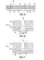
- Figs. 15-17 diagrammatically show a stamp 30 according to a fourth preferred embodiment of the present invention.
- the stamp 30 comprises a base layer 110 and a flexible stamping layer 120.
- the base layer 110 contains capillaries 170, which extend through the base layer 110 at a certain mutual distance, such that each capillary 170 is associated with an individual portion of the stamping layer 120. These individual portions are provided with a protrusion 23 having a rectangular circumference, serving as a printing dot.
- each capillary 170 at its end 171 at the side of the top surface 111 of the base layer 110, each capillary 170 comprises a funnel 172. The length of the capillaries 170 corresponds to the thickness of the base layer 110.
- the base layer 110 may be manufactured from one or more silicon wafers in which the capillaries 170 have been etched. Preferably, at its end 173 at a bottom surface 12 of the base layer 110, each capillary 170 is closed by a piezo-element (not shown), which may be constructed on a second silicon wafer.
- the entire bottom surface 22 of the stamping layer 120 is held against the top surface 111 of the base layer 110, except for the portions which are associated with the capillaries 170.
- vacuum suction may be utilized, which is particularly advantageous if the stamping layer 120 has to be replaced for maintenance or because of wear.
- a printing action is performed by varying the pressure in the capillaries 170.
- a certain printing dot 123 can be pushed out by increasing the pressure in the associated capillary 170 above the ambient pressure, whereas the printing dot 123 can be retracted by reducing the pressure in the capillary 170 below the ambient pressure.
- a pushed out position of a printing dot 123 is shown in Fig. 16
- a retracted position of a printing dot 123 is shown in Fig. 17 .
- the capillaries 170 may be filled with liquid or gas. Liquid is preferred, as liquid may be chosen to be the patterning ink. In such case, the stamping layer 120 is made permeable to the liquid, wherein the liquid in the capillary 170 does not only serve to exert a pressing force on portions of the stamping layer 120, but also to impregnate the stamp 30.
- the pressure in a capillary 170 is increased, an associated printing dot 123 is moved outwards as long as the pressure loss in the porous stamping layer 120 is higher than the pressure needed to actuate.
- ink is oozing through the porous stamping layer 120, and exits on stamping surface 31.
- the pressure in the capillaries 170 is individually controlled by a suitable control device (not shown), which may comprise a computer.
- the printing dot 123 has a rectangular circumference, whereby rectangular local contact is established between the stamping surface 31 and the receiving surface 21 during a printing action.
- the circumference of the printing dot 123 has a different shape, or even that the printing dot 123 is entirely left out. In the latter case, circular local contact is established between the stamping surface 31 and the receiving surface 21 during a printing action, as the circumference of the funnel 172 of the capillary 170 is circular.
- Figs. 18-20 diagrammatically show portions of a stamp 30 according to a fifth preferred embodiment of the present invention.
- portions of the stamping surface 31 associated with the capillaries 170 are buckled at rest, in the inward direction.
- a portion in a rest position is shown in Fig. 18 .
- This particular rest position can for instance be obtained by putting the stamping layer 120 into contact with the base layer 110 at a lower temperature than the working temperature. In case of the temperature being brought to the working temperature for the purpose of a printing action, the stamping layer 120 expands and buckles into the funnels 172 of the capillaries 170.
- a buckle is bi-stable. Therefore, if the pressure in a certain capillary 170 is increased, an associated buckled portion of the stamping layer 120 at a certain point switches over to a pushed out position. In Fig. 19 , a buckled portion in the pushed out position is shown, touching the receiving surface 21 of a substrate 20.
- the buckled portion When the buckled portion is in the pushed out position as shown in Fig. 19 , and the pressure exerted by the associated capillary 170 is still increased, the buckled portion is brought into an enhanced pushed out position, wherein the contact surface between the buckled portion and the receiving surface 21 is increased, as shown in Fig. 20 .
- this technique of still increasing the pressure it is possible to modulate the size of a single printed dot on the receiving surface 21, thereby optimizing and speeding up the printing of the entire receiving surface 21.
- Fig. 21 diagrammatically shows a sectional view of a portion of a stamp 30, wherein the base layer 110 is provided with notches 113 for receiving protrusions 124 being situated at the bottom surface 22 of the stamping layer 120. In this way, good fixation of the stamping layer 120 on the base layer 110 is ensured.
- the notches 113 and the protrusions 124 are preferably made into trenches that completely surround a printing dot 123 and the associated funnel 172.
- the trenches may have a rectangular circumference, as shown in Fig. 22 , which shows a bottom view of a portion of the stamp 4, wherein the notch 13, the protrusion 24 and the upper circumference of the funnel 172 are depicted by means of dashed lines.
- the stamping layer 120 may be desirable to allow pressure to leak from one portion associated with a capillary 170 to an adjacent portion, for instance in order to allow printing in continuous lines by controlling the pressure in the capillaries 170 such that rows of portions of the stamping layer 120 associated with the capillaries 170 are subjected to more or less the same pressure.
- the notches 113 and the protrusions 124 formed as trenches may be left out.
- Fig. 23 A possibility for aligning square printing dots 23 is shown in Fig. 23 .
- the length L of the sides of the printing dots 23 is 1 ⁇ m, and the printing dots 23 are positioned in pairs at a mutual distance D of 2 ⁇ m. Subsequent pairs of printing dots 23 are mutually displaced at an effective pitch P of 0.5 ⁇ m.
- the printing dots 23 are positioned in two rows of six pairs each, wherein said two rows are positioned at a mutual distance R of 1.5 ⁇ m.
- the substrate 30, which is not shown in Fig. 23 is moved in the direction in which the pairs of printing dots 23 are positioned in the rows, as indicated by arrow M in Fig. 23 .
- the substrate 30 may be moved at discrete steps of 1 ⁇ m.
- Fig. 23 shows only one of the many possibilities of the pattern according to which the printing dots 23 may be positioned. It will further be understood that the actuators 60 are positioned according to a corresponding pattern. In case of the printing dots 23 not being present, the alignment of the actuators 60 determines the possibilities for the pattern to be printed.
- Fig. 24 an example is shown of a printed pattern being obtained by using a stamp having printing dots 23 which are aligned in the way as shown in Fig. 23 .
- the lines in the pattern indicate prints of the sides of the printing dots 23 that are utilized.
- the maximum distance between the lines is 0.5 ⁇ m in both directions, indicating that overlapping printing dots 23 have been utilized.
- the pitch P could be as large as ten times the length L of the sides of the printing dots 23. In case of the length L being 1 ⁇ m, the pitch P would then be 10 ⁇ m. With such an alignment of the printing dots 23, the printing dots 23 need to be printed at 100 positions to cover an entire receiving surface 21. If the printing dots 23 are moved at a frequency of 50 Hz, printing of one substrate 20 would take 2 seconds.
- a wave printing apparatus of the kind shown in Fig. 1 however with capillaries as shown in Fig. 15 was used for transferring a fluid layer.
- the capillaries were filled with air at a low pressure.
- the base layer and the stamping surface were held together in through vacuum suction.
- the stamping surface was brought towards the receiving surface through the provision of air into the capillaries.
- a solution of Fe(NO 3 ) 3 .9H 2 O in water was provided on the stamping surface. Hereafter the solvent was evaporated passively for about 30 seconds. Then local areas of the stamping surface were brought to the receiving surface one after the other, according to a wave pattern.
- the fluid layer of iron nitrate was transferred to the receiving surface. Subsequently, carbon nanotubes were grown selectively. These were found to adhere only at the transferred areas. This shows that the transfer of the fluid layer was successful and provided the desired pattern.
- a solution of organometallic compounds in a polar solvent was used.
- the metallic compound was silver.
- Colloidal silver (6g, ex Merck) was added to 20 g of water and rolled for one night on a roller conveyer and the sol dispersion was filtered over a 200 nm filter.
- a composition contained 40 mg methyl trimethoxysilane (MTMS), 0.86 g tetraethoxysilane (TES), 32 g water, 4.5 g ethanol and 0.14 g glacial acetic acid. It was hydrolyzed for 48 h.
- the silver sol was cured at 250 °C for 30 minutes, followed by a further heat treatments at 350, 450, 500 and 550 °C for 30 minutes.
- the resulting pattern showed silver lines having a width of about 40 ⁇ m. No bulges or deformations of the lines could be observed.
- the substrate 20 and the stamp 30 can have any suitable shape.
- the present invention is in the first place intended to be applied in situations where substrates 20 having substantially flat receiving surfaces 21 are utilized. Nevertheless, the present invention is also suitable to be applied in other situations, for example where substrates 20 having a convex receiving surface 21 are utilized.
- the actuators are arranged so as to act in a direction substantially perpendicular to the receiving surface 21.
- transfer areas between a stamping surface 31 and a receiving surface 21 are created by successively moving portions of the stamping surface 31 in the direction of the receiving surface 21 or by successively moving portions of the receiving surface 21 in the direction of the stamping surface 31. It is also possible to move corresponding portions of the stamping surface 31 as well as the receiving surface 21 simultaneously in order to create the transfer areas.
- the stamp 30 can be mounted on a carrier.
- a carrier can for example be shaped like a cylinder or a part of a cylinder having a relatively large diameter.
- a carrier provides the stamp 30 with stiffness in the x-direction and the y-direction, and not in the z-direction.
Landscapes
- Engineering & Computer Science (AREA)
- Nanotechnology (AREA)
- Chemical & Material Sciences (AREA)
- Physics & Mathematics (AREA)
- Crystallography & Structural Chemistry (AREA)
- General Physics & Mathematics (AREA)
- Condensed Matter Physics & Semiconductors (AREA)
- Theoretical Computer Science (AREA)
- Mathematical Physics (AREA)
- Manufacturing & Machinery (AREA)
- Mechanical Engineering (AREA)
- Printing Methods (AREA)
- Shaping Of Tube Ends By Bending Or Straightening (AREA)
- Application Of Or Painting With Fluid Materials (AREA)
- Decoration By Transfer Pictures (AREA)
- Manufacturing Optical Record Carriers (AREA)
Claims (19)
- Soft-Lithographie-Druckverfahren zur Übertragung einer Struktur (34) auf eine Aufnahmefläche (21) eines Substrats (20), in dem ein Stempel (30, 301, 302) mit einer Stempelfläche (31) verwendet wird, wobei zumindest die Stempelfläche oder die Aufnahmefläche flexibel ist, wobei das Verfahren die folgenden Schritte umfasst, wonach:- der Stempel und das Substrats relativ zueinander so positioniert werden, dass die Stempelfläche und die Aufnahmefläche einander zugewandt sind;- die Positionen des Stempels und des Substrats in einer Richtung, in der sich die Aufnahmefläche erstreckt, relativ zueinander fixiert werden;
wobei das Verfahren dadurch gekennzeichnet ist, dass- ein erster Teil von zumindest der Stempelfläche oder der Aufnahmefläche in einer Richtung im Wesentlichen senkrecht zu der Aufnahmefläche vorwärts und rückwärts bewegt wird, so dass während einer ersten Übertragungsperiode eine erste Übertragungsfläche zwischen der Stempelfläche und der Aufnahmefläche erzeugt wird, auf welcher der Stempel die Struktur auf das Substrat lokal übertragen kann; und- ein zweiter Teil von zumindest der Stempelfläche oder der Aufnahmefläche in einer Richtung im Wesentlichen senkrecht zu der Aufnahmefläche vorwärts und rückwärts bewegt wirkt, so dass während einer zweiten Übertragungsperiode eine zweite Übertragungsfläche zwischen der Stempelfläche und der Aufnahmefläche erzeugt wird, auf welcher der Stempel die Struktur auf das Substrat lokal übertragen kann. - Verfahren nach Anspruch 1, wobei die Dauer der ersten Übertragungsperiode und die Dauer der zweiten Übertragungsperiode einander im Wesentlichen gleichen.
- Verfahren nach Anspruch 2, wobei sich die erste Übertragungsperiode und die zweite Übertragungsperiode zum Teil überschneiden.
- Verfahren nach einem der Ansprüche 1-3, wobei der erste Teil und der zweite Teil aneinandergrenzende Teile sind.
- Verfahren nach Anspruch 1, wobei die Struktur auf der Stempelfläche des Stempels vorgesehen wird.
- Verfahren nach Anspruch 1, wobei zumindest die zweite Übertragungsfläche wie ein Ring geformt ist.
- Verfahren nach Anspruch 1, wobei die erste Übertragungsfläche und die zweite Übertragungsfläche linear sind.
- Verfahren nach Anspruch 1, wobei der erste Teil und der zweite Teil sukzessiv einem Druck unterworfen werden, um den ersten Teil und den zweiten Teil sukzessiv zu bewegen.
- Vorrichtung (1, 2) zur Übertragung einer Struktur (34) von einer Stempelfläche (31) eines Soft-Lithographie-Stempels (30, 301, 302) auf eine Aufnahmefläche (21) eines Substrats (20) gemäß dem Verfahren nach einem der Ansprüche 1-8, wobei die Vorrichtung umfasst:- einen Soft-Lithographie-Stempel (30) mit einer eine Struktur (34) aufweisenden Stempelfläche (31), gekennzeichnet durch:- Mittel (50-53, 72; 73), die so angeordnet sind, dass sich einzelne Teile von zumindest der Stempelfläche oder der Aufnahmefläche in einer Richtung im Wesentlichen senkrecht zu der Aufnahmefläche sukzessiv vorwärts und rückwärts bewegen können.
- Vorrichtung (1, 2) nach Anspruch 9, die weiterhin eine Steuereinrichtung zur Steuerung der Mittel (50-53, 72; 73) umfasst, in der ein der gewünschten Struktur zugeordnetes Steuerprogramm gespeichert ist.
- Vorrichtung (1, 2) nach Anspruch 9 oder 10, wobei die Mittel (50-53, 72; 73) individuell steuerbar sind.
- Vorrichtung (1, 2) nach Anspruch 9 oder 10, wobei die Mittel (50-53, 72; 73) so angeordnet sind, dass sie in einer Richtung im Wesentlichen senkrecht zu der Aufnahmefläche (21) wirken.
- Vorrichtung (1, 2) nach Anspruch 9 oder 10, wobei die Mittel mehrere Aktuatoren (50-53) umfassen, wobei jeder Aktuator einem einzelnen Segment von zumindest der Stempelfläche (31) oder der Aufnahmefläche (21) zugeordnet ist.
- Vorrichtung nach Anspruch 9 oder 10, wobei die Mittel Kanäle (73) umfassen, die Vakuumkammern (72) zugeordnet sind.
- Vorrichtung (1, 2) nach Anspruch 9 oder 10, die weiterhin Ausrichtmittel (60; 61; 62) umfasst, um die Stempelfläche (31) und die Aufnahmefläche (21) relativ zueinander auszurichten.
- Soft-Lithographie-Stempel (30, 301) zur Verwendung in der Vorrichtung (1) nach Anspruch 9, wobei der Stempel eine eine Struktur aufweisende Stempelfläche (31) hat und umfasst:- eine Basisfläche (37); dadurch gekennzeichnet, dass die Stempelfläche in aneinandergrenzende einzelne Stempelteile (40) unterteilt ist, die zumindest einen Teil der Basisschicht bedecken, von denen eine Oberseite mit einem Teil der Struktur versehen und eine Unterseite mit der Basisfläche verbunden ist, wobei die einzelnen Stempelteile mit Hilfe der Mittel (50-53, 72; 73) in einer Richtung im Wesentlichen senkrecht zu der Aufnahmefläche (21) eines Substrats (20) vorwärts und rückwärts bewegbar sind, wenn diese so in der Vorrichtung (1) platziert sind, dass die Stempelfläche der Aufnahmefläche zugewandt ist.
- Stempel (301) nach Anspruch 16, wobei die Basisfläche (37) wie eine geschlossene Schleife geformt ist.
- Soft-Lithographie-Stempel (302) zur Verwendung in der Vorrichtung (2) nach Anspruch 9, wobei der Stempel eine eine Struktur (34) mit Merkmalen in dem Mikrometer- oder Submikrometerbereich aufweisende Stempelfläche (39) umfasst, dadurch gekennzeichnet, dass der Stempel eine Druckfläche (43) umfasst, die mit sich in einer Richtung im Wesentlichen senkrecht zu der Stempelfläche erstreckenden Kanälen (44) versehen ist, wobei unterschiedliche Segmente der Stempelfläche unterschiedlichen Kanälen zugeordnet sind, so dass jedes der Segmente durch jeweiliges Ausüben eines Überdrucks und eines Unterdrucks auf seinen zugeordneten Kanal in einer Richtung im Wesentlichen senkrecht zu der Aufnahmefläche (21) eines Substrats (20) individuell vorwärts und rückwärts bewegbar ist, wenn der Stempel so in der Vorrichtung (2) platziert ist, dass die Stempelfläche der Aufnahmefläche zugewandt ist.
- Stempel (302) nach Anspruch 18, wobei die Länge der Kanäle (44) der Dicke der Druckfläche (43) entspricht.
Priority Applications (1)
| Application Number | Priority Date | Filing Date | Title |
|---|---|---|---|
| EP03727761A EP1511632B1 (de) | 2002-05-27 | 2003-05-26 | Verfahren und vorrichtung zur übertragung eines musters von einem stempel auf ein substrat |
Applications Claiming Priority (6)
| Application Number | Priority Date | Filing Date | Title |
|---|---|---|---|
| EP02077079 | 2002-05-27 | ||
| EP02077087 | 2002-05-27 | ||
| EP02077087 | 2002-05-27 | ||
| EP02077079 | 2002-05-27 | ||
| EP03727761A EP1511632B1 (de) | 2002-05-27 | 2003-05-26 | Verfahren und vorrichtung zur übertragung eines musters von einem stempel auf ein substrat |
| PCT/IB2003/002003 WO2003099463A2 (en) | 2002-05-27 | 2003-05-26 | Method and device for transferring a pattern from a stamp to a substrate |
Publications (2)
| Publication Number | Publication Date |
|---|---|
| EP1511632A2 EP1511632A2 (de) | 2005-03-09 |
| EP1511632B1 true EP1511632B1 (de) | 2011-11-02 |
Family
ID=29585707
Family Applications (1)
| Application Number | Title | Priority Date | Filing Date |
|---|---|---|---|
| EP03727761A Expired - Lifetime EP1511632B1 (de) | 2002-05-27 | 2003-05-26 | Verfahren und vorrichtung zur übertragung eines musters von einem stempel auf ein substrat |
Country Status (8)
| Country | Link |
|---|---|
| US (1) | US7296519B2 (de) |
| EP (1) | EP1511632B1 (de) |
| JP (1) | JP4639081B2 (de) |
| KR (1) | KR100981692B1 (de) |
| CN (1) | CN100358728C (de) |
| AT (1) | ATE532099T1 (de) |
| AU (1) | AU2003232962A1 (de) |
| WO (1) | WO2003099463A2 (de) |
Families Citing this family (80)
| Publication number | Priority date | Publication date | Assignee | Title |
|---|---|---|---|---|
| JP4340086B2 (ja) * | 2003-03-20 | 2009-10-07 | 株式会社日立製作所 | ナノプリント用スタンパ、及び微細構造転写方法 |
| DE10330456B9 (de) * | 2003-07-05 | 2007-11-08 | Erich Thallner | Vorrichtung zum Erstellen einer Oberflächenstruktur auf einem Wafer |
| US7632087B2 (en) * | 2003-12-19 | 2009-12-15 | Wd Media, Inc. | Composite stamper for imprint lithography |
| US6981445B2 (en) * | 2003-12-24 | 2006-01-03 | Axela Biosensors Inc. | Method and apparatus for micro-contact printing |
| CN102004393B (zh) * | 2004-04-27 | 2013-05-01 | 伊利诺伊大学评议会 | 用于软光刻法的复合构图设备 |
| WO2005109535A2 (en) * | 2004-05-06 | 2005-11-17 | Koninklijke Philips Electronics N.V. | A method of manufacturing a thermoelectric device |
| JP2008505475A (ja) * | 2004-06-30 | 2008-02-21 | コーニンクレッカ フィリップス エレクトロニクス エヌ ヴィ | 化学的にパターン処理された表面を有するソフトリソグラフィー用スタンプ |
| US20070164476A1 (en) * | 2004-09-01 | 2007-07-19 | Wei Wu | Contact lithography apparatus and method employing substrate deformation |
| WO2006043244A1 (en) | 2004-10-22 | 2006-04-27 | Koninklijke Philips Electronics N.V. | Roller micro-contact printer with pressure control |
| US20110104840A1 (en) | 2004-12-06 | 2011-05-05 | Koninklijke Philips Electronics, N.V. | Etchant Solutions And Additives Therefor |
| EP1669196B1 (de) * | 2004-12-10 | 2008-05-21 | ESSILOR INTERNATIONAL (Compagnie Générale d'Optique) | Stempel zum Auftragen eines Motivs, Verfahren zur Stempelherstellung und Verfahren zur Herstellung eines Objekts anhand von diesem Stempel |
| US7410591B2 (en) | 2004-12-16 | 2008-08-12 | Asml Holding N.V. | Method and system for making a nano-plate for imprint lithography |
| US7409759B2 (en) | 2004-12-16 | 2008-08-12 | Asml Holding N.V. | Method for making a computer hard drive platen using a nano-plate |
| US7399422B2 (en) | 2005-11-29 | 2008-07-15 | Asml Holding N.V. | System and method for forming nanodisks used in imprint lithography and nanodisk and memory disk formed thereby |
| US7363854B2 (en) | 2004-12-16 | 2008-04-29 | Asml Holding N.V. | System and method for patterning both sides of a substrate utilizing imprint lithography |
| US7331283B2 (en) | 2004-12-16 | 2008-02-19 | Asml Holding N.V. | Method and apparatus for imprint pattern replication |
| US7676088B2 (en) | 2004-12-23 | 2010-03-09 | Asml Netherlands B.V. | Imprint lithography |
| WO2006083518A2 (en) * | 2005-01-31 | 2006-08-10 | Molecular Imprints, Inc. | Chucking system for nano-manufacturing |
| US7636999B2 (en) * | 2005-01-31 | 2009-12-29 | Molecular Imprints, Inc. | Method of retaining a substrate to a wafer chuck |
| KR101256383B1 (ko) | 2005-05-03 | 2013-04-25 | 코닌클리케 필립스 일렉트로닉스 엔.브이. | 스탬프로부터 기판으로 패턴을 전사하기 위한 방법 및디바이스 |
| JP4596981B2 (ja) * | 2005-05-24 | 2010-12-15 | 株式会社日立ハイテクノロジーズ | インプリント装置、及び微細構造転写方法 |
| KR100903097B1 (ko) * | 2005-06-13 | 2009-06-15 | 한국기계연구원 | 균일압으로 패턴 성형이 가능한 임프린팅장치 |
| US20070178237A1 (en) * | 2005-08-02 | 2007-08-02 | Shin Dong M | Method for patterning coatings |
| US20070035717A1 (en) * | 2005-08-12 | 2007-02-15 | Wei Wu | Contact lithography apparatus, system and method |
| US20070048448A1 (en) * | 2005-08-17 | 2007-03-01 | Kim Dae H | Patterning method using coatings containing ionic components |
| EP1764648B1 (de) | 2005-09-14 | 2012-05-23 | Thallner, Erich, Dipl.-Ing. | Stempel mit einer Nanostempelstruktur sowie Vorrichtung und Verfahren zu dessen Herstellung |
| US7677877B2 (en) | 2005-11-04 | 2010-03-16 | Asml Netherlands B.V. | Imprint lithography |
| JP2007134368A (ja) * | 2005-11-08 | 2007-05-31 | Nikon Corp | パターン転写装置、露光装置及びパターン転写方法 |
| US7906058B2 (en) * | 2005-12-01 | 2011-03-15 | Molecular Imprints, Inc. | Bifurcated contact printing technique |
| WO2007067488A2 (en) | 2005-12-08 | 2007-06-14 | Molecular Imprints, Inc. | Method and system for double-sided patterning of substrates |
| US7707937B2 (en) * | 2005-12-15 | 2010-05-04 | Palo Alto Research Center Incorporated | Digital impression printing system |
| US7517211B2 (en) | 2005-12-21 | 2009-04-14 | Asml Netherlands B.V. | Imprint lithography |
| JP4814682B2 (ja) * | 2006-04-18 | 2011-11-16 | 株式会社日立ハイテクノロジーズ | 微細構造パターンの転写方法及び転写装置 |
| JP4854383B2 (ja) * | 2006-05-15 | 2012-01-18 | アピックヤマダ株式会社 | インプリント方法およびナノ・インプリント装置 |
| JP4996150B2 (ja) * | 2006-07-07 | 2012-08-08 | 株式会社日立ハイテクノロジーズ | 微細構造転写装置および微細構造転写方法 |
| JP4449949B2 (ja) * | 2006-07-18 | 2010-04-14 | セイコーエプソン株式会社 | 表面エネルギー差バンクの形成方法、パターンの形成方法、バンク構造、電子回路、電子デバイス、電子機器、及びスタンプ |
| US7946837B2 (en) * | 2006-10-06 | 2011-05-24 | Asml Netherlands B.V. | Imprint lithography |
| US9440254B2 (en) | 2006-12-04 | 2016-09-13 | Koninklijke Philips N.V. | Method and apparatus for applying a sheet to a substrate |
| CN101583436B (zh) * | 2007-01-16 | 2014-05-07 | 皇家飞利浦电子股份有限公司 | 用于挠性板件和基板接触的方法和系统 |
| GB0701909D0 (en) * | 2007-01-31 | 2007-03-14 | Imp Innovations Ltd | Deposition Of Organic Layers |
| KR20100016643A (ko) * | 2007-04-19 | 2010-02-12 | 바스프 에스이 | 기판 상에 패턴을 형성하는 방법 및 그에 의해 형성된 전자 장치 |
| US20080309900A1 (en) * | 2007-06-12 | 2008-12-18 | Micron Technology, Inc. | Method of making patterning device, patterning device for making patterned structure, and method of making patterned structure |
| JP5041214B2 (ja) * | 2007-06-15 | 2012-10-03 | ソニー株式会社 | 金属薄膜の形成方法および電子デバイスの製造方法 |
| JP5045263B2 (ja) * | 2007-06-20 | 2012-10-10 | ソニー株式会社 | 印刷装置および印刷方法 |
| NL1036034A1 (nl) | 2007-10-11 | 2009-04-15 | Asml Netherlands Bv | Imprint lithography. |
| GB2453766A (en) * | 2007-10-18 | 2009-04-22 | Novalia Ltd | Method of fabricating an electronic device |
| JP6088138B2 (ja) | 2008-06-06 | 2017-03-01 | コーニンクレッカ フィリップス エヌ ヴェKoninklijke Philips N.V. | シリコーンラバー状材料を含むパターンが形成されたスタンプ層の製造方法、スタンプ層、及びスタンプ層を含む印刷デバイス |
| US7927976B2 (en) * | 2008-07-23 | 2011-04-19 | Semprius, Inc. | Reinforced composite stamp for dry transfer printing of semiconductor elements |
| KR101633637B1 (ko) | 2008-10-10 | 2016-06-27 | 코닌클리케 필립스 엔.브이. | 광 방향성 센서 |
| JP5261845B2 (ja) * | 2008-10-28 | 2013-08-14 | 株式会社ブイ・テクノロジー | 欠陥修正方法 |
| US8506867B2 (en) * | 2008-11-19 | 2013-08-13 | Semprius, Inc. | Printing semiconductor elements by shear-assisted elastomeric stamp transfer |
| JP2011005773A (ja) * | 2009-06-26 | 2011-01-13 | Fuji Electric Device Technology Co Ltd | インプリント用スタンパおよびインプリント装置 |
| US8261660B2 (en) | 2009-07-22 | 2012-09-11 | Semprius, Inc. | Vacuum coupled tool apparatus for dry transfer printing semiconductor elements |
| KR101790367B1 (ko) | 2009-12-22 | 2017-10-25 | 쓰리엠 이노베이티브 프로퍼티즈 컴파니 | 가압 롤러를 사용한 미세 접촉 인쇄 장치 및 방법 |
| CN101807004B (zh) * | 2010-03-08 | 2012-07-11 | 彩虹集团电子股份有限公司 | 一种用于彩色显像管网版生产的工作版的制做方法 |
| JP5618588B2 (ja) * | 2010-03-24 | 2014-11-05 | キヤノン株式会社 | インプリント方法 |
| US9765934B2 (en) | 2011-05-16 | 2017-09-19 | The Board Of Trustees Of The University Of Illinois | Thermally managed LED arrays assembled by printing |
| DE102011054789A1 (de) * | 2011-10-25 | 2013-04-25 | Universität Kassel | Nano-Formgebungsstruktur |
| JP6086675B2 (ja) * | 2011-11-30 | 2017-03-01 | 株式会社Screenホールディングス | 印刷装置および印刷方法 |
| JP5759348B2 (ja) * | 2011-11-30 | 2015-08-05 | 株式会社Screenホールディングス | パターン形成装置およびパターン形成方法 |
| JP5925505B2 (ja) * | 2012-02-03 | 2016-05-25 | セーレン株式会社 | 微細ドットパターンの印刷方法 |
| CN103373094A (zh) * | 2012-04-11 | 2013-10-30 | 得利环球有限公司 | 微接触印刷设备及方法 |
| CN102866582B (zh) * | 2012-09-29 | 2014-09-10 | 兰红波 | 一种用于高亮度led图形化的纳米压印装置和方法 |
| JP6207997B2 (ja) * | 2013-01-30 | 2017-10-04 | 株式会社Screenホールディングス | パターン形成装置およびパターン形成方法 |
| CN106462054B (zh) * | 2014-03-31 | 2020-07-07 | 皇家飞利浦有限公司 | 压印方法、用于压印方法的计算机程序产品和装置 |
| JP6684783B2 (ja) * | 2014-09-22 | 2020-04-22 | コーニンクレッカ フィリップス エヌ ヴェKoninklijke Philips N.V. | 転写方法、装置及びコンピュータプログラム製品 |
| US20170363953A1 (en) * | 2014-11-03 | 2017-12-21 | Universität Osnabrück | Device for carrying out a capillary nanoprinting method, a method for carrying out capillary nanoprinting using the device, products obtained according to the method and use of the device |
| US11163230B2 (en) | 2016-04-06 | 2021-11-02 | Koninklijke Philips N.V. | Imprint lithography stamp method of making and using the same |
| KR102328775B1 (ko) | 2016-07-14 | 2021-11-22 | 모포토닉스 홀딩 비.브이. | 가요성 스탬프로 개별 기판을 임프린트하기 위한 장치 |
| CN109600996B (zh) * | 2016-07-27 | 2021-11-30 | 皇家飞利浦有限公司 | 基于聚有机硅氧烷的印模、其制造方法、其用于印刷工艺的用途以及利用其的压印方法 |
| CN107215111B (zh) * | 2017-06-14 | 2023-03-28 | 浙江大学 | 一种磁控转印印章及磁控转移印刷方法 |
| EP3881134B1 (de) | 2018-11-14 | 2022-07-20 | Koninklijke Philips N.V. | Pneumatisches system, prägegerät und deren anwendung |
| US20220223451A1 (en) * | 2019-05-22 | 2022-07-14 | Vuereal Inc. | Systems and methods for transferring devices or patterns to a substrate |
| CN111430272B (zh) * | 2020-03-09 | 2023-02-03 | 广东工业大学 | 单类和多类微小物体悬浮定向移动及自主装巨量转移方法 |
| WO2023001802A1 (en) * | 2021-07-21 | 2023-01-26 | Koninklijke Philips N.V. | Imprinting apparatus |
| EP4123376A1 (de) * | 2021-07-21 | 2023-01-25 | Koninklijke Philips N.V. | Prägevorrichtung |
| US12259660B2 (en) * | 2021-10-26 | 2025-03-25 | Industrial Technology Research Institute | Inspection method and inspection platform for lithography |
| EP4390539A1 (de) | 2022-12-19 | 2024-06-26 | Koninklijke Philips N.V. | Ausrichtungsverfahren für imprintverfahren |
| EP4390540A1 (de) | 2022-12-19 | 2024-06-26 | Koninklijke Philips N.V. | Ausrichtungsverfahren |
| US20240427236A1 (en) * | 2023-06-26 | 2024-12-26 | Google Llc | Process control pattern to improve nanoimprint detaching process |
Family Cites Families (17)
| Publication number | Priority date | Publication date | Assignee | Title |
|---|---|---|---|---|
| DE94221C (de) * | ||||
| US1527921A (en) | 1923-05-22 | 1925-02-24 | Auto Mark Corp | Printing device |
| DE1103357B (de) * | 1955-01-24 | 1961-03-30 | Konrad Elsaesser | Vorrichtung zum Bedrucken oder Bestempeln von Markenetiketten |
| GB1005502A (en) * | 1963-04-17 | 1965-09-22 | Ellicock & Healy Ltd | Improvements in or relating to printing blocks for printing machines |
| US5352651A (en) * | 1992-12-23 | 1994-10-04 | Minnesota Mining And Manufacturing Company | Nanostructured imaging transfer element |
| US5900160A (en) * | 1993-10-04 | 1999-05-04 | President And Fellows Of Harvard College | Methods of etching articles via microcontact printing |
| JP3372258B2 (ja) * | 1995-08-04 | 2003-01-27 | インターナシヨナル・ビジネス・マシーンズ・コーポレーシヨン | リソグラフィ・プロセス用のスタンプ |
| WO1997006013A1 (en) * | 1995-08-04 | 1997-02-20 | International Business Machines Corporation | Lithographic surface or thin layer modification |
| JPH09263028A (ja) * | 1996-01-25 | 1997-10-07 | Hiroyuki Koike | 回転式印字器及び回転式印字器に用いる帯状体の製造方法 |
| US5669303A (en) * | 1996-03-04 | 1997-09-23 | Motorola | Apparatus and method for stamping a surface |
| US6129016A (en) * | 1998-04-03 | 2000-10-10 | Rehkemper; Steven | Stamping toy having indexing means |
| US20020043170A1 (en) * | 2000-01-10 | 2002-04-18 | Rafael Bronstein | System and method for preparing and utilizing a printing member having magnetic particles therein |
| EP1171800B1 (de) * | 2000-02-07 | 2006-04-19 | Koninklijke Philips Electronics N.V. | Stempel für ein lithographisches verfahren, methode zur stempelherstellung und methode zur herstellung einer gemusterten schicht auf einem substrat |
| JP2002273996A (ja) * | 2001-03-21 | 2002-09-25 | Yamahachi Chemical Co Ltd | 複数の印面を有する液浸透式スタンプ |
| US7117790B2 (en) * | 2002-01-11 | 2006-10-10 | Massachusetts Institute Of Technology | Microcontact printing |
| US7037458B2 (en) * | 2003-10-23 | 2006-05-02 | Intel Corporation | Progressive stamping apparatus and method |
| KR100585951B1 (ko) * | 2004-02-18 | 2006-06-01 | 한국기계연구원 | 조합/분리형 독립구동이 가능한 복수 개의 모듈을 갖는 임프린팅 장치 |
-
2003
- 2003-05-26 AU AU2003232962A patent/AU2003232962A1/en not_active Abandoned
- 2003-05-26 CN CNB038123967A patent/CN100358728C/zh not_active Expired - Lifetime
- 2003-05-26 AT AT03727761T patent/ATE532099T1/de active
- 2003-05-26 EP EP03727761A patent/EP1511632B1/de not_active Expired - Lifetime
- 2003-05-26 US US10/515,687 patent/US7296519B2/en not_active Expired - Lifetime
- 2003-05-26 WO PCT/IB2003/002003 patent/WO2003099463A2/en not_active Ceased
- 2003-05-26 JP JP2004506978A patent/JP4639081B2/ja not_active Expired - Lifetime
- 2003-05-26 KR KR1020047019102A patent/KR100981692B1/ko not_active Expired - Lifetime
Also Published As
| Publication number | Publication date |
|---|---|
| KR20050016441A (ko) | 2005-02-21 |
| AU2003232962A1 (en) | 2003-12-12 |
| ATE532099T1 (de) | 2011-11-15 |
| WO2003099463A3 (en) | 2004-09-16 |
| WO2003099463A2 (en) | 2003-12-04 |
| US20050173049A1 (en) | 2005-08-11 |
| KR100981692B1 (ko) | 2010-09-13 |
| EP1511632A2 (de) | 2005-03-09 |
| US7296519B2 (en) | 2007-11-20 |
| JP4639081B2 (ja) | 2011-02-23 |
| CN100358728C (zh) | 2008-01-02 |
| JP2005527406A (ja) | 2005-09-15 |
| AU2003232962A8 (en) | 2003-12-12 |
| CN1665684A (zh) | 2005-09-07 |
Similar Documents
| Publication | Publication Date | Title |
|---|---|---|
| EP1511632B1 (de) | Verfahren und vorrichtung zur übertragung eines musters von einem stempel auf ein substrat | |
| EP2016613B1 (de) | System zur Lithographie durch Nanoprägung | |
| US7931187B2 (en) | Injection molded solder method for forming solder bumps on substrates | |
| EP2091666B1 (de) | Verfahren und vorrichtung zum anbringen eines blattes auf einem substrat | |
| US5817242A (en) | Stamp for a lithographic process | |
| CN100559271C (zh) | 将图案从印模转印到基体的方法和装置 | |
| US7632087B2 (en) | Composite stamper for imprint lithography | |
| US20040197712A1 (en) | System for contact printing | |
| US5947027A (en) | Printing apparatus with inflatable means for advancing a substrate towards the stamping surface | |
| CN1800974B (zh) | 压印光刻 | |
| JPH09240125A (ja) | 物品の面をスタンピングするための装置および方法 | |
| CN103635330B (zh) | 用于制备、着墨和安装用于微接触印刷的压模的方法 | |
| EP1801650A2 (de) | Ausrichtung für Imprint-Lithographie | |
| US20080271625A1 (en) | High-Throughput Apparatus for Patterning Flexible Substrates and Method of Using the Same | |
| JP2011044715A (ja) | 基板のエンボス加工用装置 | |
| KR100837339B1 (ko) | 탄성중합체 스탬프를 이용한 롤 프린트 방식의 미세접촉인쇄장치 | |
| KR101551772B1 (ko) | Scil 공정용 레플리카 스탬프 및 이의 제조방법 | |
| JP2004181814A (ja) | 凹版印刷装置 | |
| US20150108673A1 (en) | Imprinting apparatus and method for imprinting | |
| JP2005043677A (ja) | カラーフィルタの製造方法及び製造装置 |
Legal Events
| Date | Code | Title | Description |
|---|---|---|---|
| PUAI | Public reference made under article 153(3) epc to a published international application that has entered the european phase |
Free format text: ORIGINAL CODE: 0009012 |
|
| AK | Designated contracting states |
Kind code of ref document: A2 Designated state(s): AT BE BG CH CY CZ DE DK EE ES FI FR GB GR HU IE IT LI LU MC NL PT RO SE SI SK TR |
|
| AX | Request for extension of the european patent |
Extension state: AL LT LV MK |
|
| 17P | Request for examination filed |
Effective date: 20050316 |
|
| DAX | Request for extension of the european patent (deleted) | ||
| 17Q | First examination report despatched |
Effective date: 20100427 |
|
| REG | Reference to a national code |
Ref country code: DE Ref legal event code: R079 Ref document number: 60338973 Country of ref document: DE Free format text: PREVIOUS MAIN CLASS: B41K0001020000 Ipc: G03F0007000000 |
|
| RIC1 | Information provided on ipc code assigned before grant |
Ipc: B41K 1/02 20060101ALI20110318BHEP Ipc: G03F 7/00 20060101AFI20110318BHEP |
|
| GRAP | Despatch of communication of intention to grant a patent |
Free format text: ORIGINAL CODE: EPIDOSNIGR1 |
|
| GRAS | Grant fee paid |
Free format text: ORIGINAL CODE: EPIDOSNIGR3 |
|
| GRAA | (expected) grant |
Free format text: ORIGINAL CODE: 0009210 |
|
| AK | Designated contracting states |
Kind code of ref document: B1 Designated state(s): AT BE BG CH CY CZ DE DK EE ES FI FR GB GR HU IE IT LI LU MC NL PT RO SE SI SK TR |
|
| REG | Reference to a national code |
Ref country code: GB Ref legal event code: FG4D |
|
| REG | Reference to a national code |
Ref country code: CH Ref legal event code: EP |
|
| REG | Reference to a national code |
Ref country code: IE Ref legal event code: FG4D |
|
| REG | Reference to a national code |
Ref country code: DE Ref legal event code: R096 Ref document number: 60338973 Country of ref document: DE Effective date: 20120105 |
|
| REG | Reference to a national code |
Ref country code: NL Ref legal event code: T3 |
|
| PG25 | Lapsed in a contracting state [announced via postgrant information from national office to epo] |
Ref country code: PT Free format text: LAPSE BECAUSE OF FAILURE TO SUBMIT A TRANSLATION OF THE DESCRIPTION OR TO PAY THE FEE WITHIN THE PRESCRIBED TIME-LIMIT Effective date: 20120302 Ref country code: SE Free format text: LAPSE BECAUSE OF FAILURE TO SUBMIT A TRANSLATION OF THE DESCRIPTION OR TO PAY THE FEE WITHIN THE PRESCRIBED TIME-LIMIT Effective date: 20111102 Ref country code: SI Free format text: LAPSE BECAUSE OF FAILURE TO SUBMIT A TRANSLATION OF THE DESCRIPTION OR TO PAY THE FEE WITHIN THE PRESCRIBED TIME-LIMIT Effective date: 20111102 Ref country code: GR Free format text: LAPSE BECAUSE OF FAILURE TO SUBMIT A TRANSLATION OF THE DESCRIPTION OR TO PAY THE FEE WITHIN THE PRESCRIBED TIME-LIMIT Effective date: 20120203 |
|
| PG25 | Lapsed in a contracting state [announced via postgrant information from national office to epo] |
Ref country code: CY Free format text: LAPSE BECAUSE OF FAILURE TO SUBMIT A TRANSLATION OF THE DESCRIPTION OR TO PAY THE FEE WITHIN THE PRESCRIBED TIME-LIMIT Effective date: 20111102 |
|
| PG25 | Lapsed in a contracting state [announced via postgrant information from national office to epo] |
Ref country code: CZ Free format text: LAPSE BECAUSE OF FAILURE TO SUBMIT A TRANSLATION OF THE DESCRIPTION OR TO PAY THE FEE WITHIN THE PRESCRIBED TIME-LIMIT Effective date: 20111102 Ref country code: DK Free format text: LAPSE BECAUSE OF FAILURE TO SUBMIT A TRANSLATION OF THE DESCRIPTION OR TO PAY THE FEE WITHIN THE PRESCRIBED TIME-LIMIT Effective date: 20111102 Ref country code: EE Free format text: LAPSE BECAUSE OF FAILURE TO SUBMIT A TRANSLATION OF THE DESCRIPTION OR TO PAY THE FEE WITHIN THE PRESCRIBED TIME-LIMIT Effective date: 20111102 Ref country code: BG Free format text: LAPSE BECAUSE OF FAILURE TO SUBMIT A TRANSLATION OF THE DESCRIPTION OR TO PAY THE FEE WITHIN THE PRESCRIBED TIME-LIMIT Effective date: 20120202 Ref country code: SK Free format text: LAPSE BECAUSE OF FAILURE TO SUBMIT A TRANSLATION OF THE DESCRIPTION OR TO PAY THE FEE WITHIN THE PRESCRIBED TIME-LIMIT Effective date: 20111102 |
|
| PG25 | Lapsed in a contracting state [announced via postgrant information from national office to epo] |
Ref country code: RO Free format text: LAPSE BECAUSE OF FAILURE TO SUBMIT A TRANSLATION OF THE DESCRIPTION OR TO PAY THE FEE WITHIN THE PRESCRIBED TIME-LIMIT Effective date: 20111102 |
|
| PLBE | No opposition filed within time limit |
Free format text: ORIGINAL CODE: 0009261 |
|
| STAA | Information on the status of an ep patent application or granted ep patent |
Free format text: STATUS: NO OPPOSITION FILED WITHIN TIME LIMIT |
|
| 26N | No opposition filed |
Effective date: 20120803 |
|
| REG | Reference to a national code |
Ref country code: DE Ref legal event code: R097 Ref document number: 60338973 Country of ref document: DE Effective date: 20120803 |
|
| PG25 | Lapsed in a contracting state [announced via postgrant information from national office to epo] |
Ref country code: MC Free format text: LAPSE BECAUSE OF NON-PAYMENT OF DUE FEES Effective date: 20120531 |
|
| REG | Reference to a national code |
Ref country code: CH Ref legal event code: PL |
|
| PG25 | Lapsed in a contracting state [announced via postgrant information from national office to epo] |
Ref country code: CH Free format text: LAPSE BECAUSE OF NON-PAYMENT OF DUE FEES Effective date: 20120531 Ref country code: LI Free format text: LAPSE BECAUSE OF NON-PAYMENT OF DUE FEES Effective date: 20120531 |
|
| REG | Reference to a national code |
Ref country code: IE Ref legal event code: MM4A |
|
| PG25 | Lapsed in a contracting state [announced via postgrant information from national office to epo] |
Ref country code: ES Free format text: LAPSE BECAUSE OF FAILURE TO SUBMIT A TRANSLATION OF THE DESCRIPTION OR TO PAY THE FEE WITHIN THE PRESCRIBED TIME-LIMIT Effective date: 20120213 Ref country code: IE Free format text: LAPSE BECAUSE OF NON-PAYMENT OF DUE FEES Effective date: 20120526 |
|
| PG25 | Lapsed in a contracting state [announced via postgrant information from national office to epo] |
Ref country code: FI Free format text: LAPSE BECAUSE OF FAILURE TO SUBMIT A TRANSLATION OF THE DESCRIPTION OR TO PAY THE FEE WITHIN THE PRESCRIBED TIME-LIMIT Effective date: 20111102 |
|
| REG | Reference to a national code |
Ref country code: DE Ref legal event code: R082 Ref document number: 60338973 Country of ref document: DE Representative=s name: VOLMER, GEORG, DIPL.-ING., DE |
|
| PG25 | Lapsed in a contracting state [announced via postgrant information from national office to epo] |
Ref country code: TR Free format text: LAPSE BECAUSE OF FAILURE TO SUBMIT A TRANSLATION OF THE DESCRIPTION OR TO PAY THE FEE WITHIN THE PRESCRIBED TIME-LIMIT Effective date: 20111102 |
|
| REG | Reference to a national code |
Ref country code: DE Ref legal event code: R081 Ref document number: 60338973 Country of ref document: DE Owner name: KONINKLIJKE PHILIPS N.V., NL Free format text: FORMER OWNER: KONINKLIJKE PHILIPS ELECTRONICS N.V., EINDHOVEN, NL Effective date: 20111115 Ref country code: DE Ref legal event code: R082 Ref document number: 60338973 Country of ref document: DE Representative=s name: VOLMER, GEORG, DIPL.-ING., DE Effective date: 20140328 Ref country code: DE Ref legal event code: R082 Ref document number: 60338973 Country of ref document: DE Representative=s name: MEISSNER, BOLTE & PARTNER GBR, DE Effective date: 20140328 Ref country code: DE Ref legal event code: R082 Ref document number: 60338973 Country of ref document: DE Representative=s name: MEISSNER BOLTE PATENTANWAELTE RECHTSANWAELTE P, DE Effective date: 20140328 Ref country code: DE Ref legal event code: R081 Ref document number: 60338973 Country of ref document: DE Owner name: KONINKLIJKE PHILIPS N.V., NL Free format text: FORMER OWNER: KONINKLIJKE PHILIPS ELECTRONICS N.V., EINDHOVEN, NL Effective date: 20140328 |
|
| PG25 | Lapsed in a contracting state [announced via postgrant information from national office to epo] |
Ref country code: LU Free format text: LAPSE BECAUSE OF NON-PAYMENT OF DUE FEES Effective date: 20120526 |
|
| PG25 | Lapsed in a contracting state [announced via postgrant information from national office to epo] |
Ref country code: HU Free format text: LAPSE BECAUSE OF FAILURE TO SUBMIT A TRANSLATION OF THE DESCRIPTION OR TO PAY THE FEE WITHIN THE PRESCRIBED TIME-LIMIT Effective date: 20030526 |
|
| REG | Reference to a national code |
Ref country code: FR Ref legal event code: CD Owner name: KONINKLIJKE PHILIPS ELECTRONICS N.V., NL Effective date: 20141126 Ref country code: FR Ref legal event code: CA Effective date: 20141126 |
|
| REG | Reference to a national code |
Ref country code: DE Ref legal event code: R082 Ref document number: 60338973 Country of ref document: DE Representative=s name: MEISSNER, BOLTE & PARTNER GBR, DE Ref country code: DE Ref legal event code: R082 Ref document number: 60338973 Country of ref document: DE Representative=s name: MEISSNER BOLTE PATENTANWAELTE RECHTSANWAELTE P, DE |
|
| REG | Reference to a national code |
Ref country code: FR Ref legal event code: PLFP Year of fee payment: 14 |
|
| REG | Reference to a national code |
Ref country code: FR Ref legal event code: PLFP Year of fee payment: 15 |
|
| REG | Reference to a national code |
Ref country code: FR Ref legal event code: PLFP Year of fee payment: 16 |
|
| PGFP | Annual fee paid to national office [announced via postgrant information from national office to epo] |
Ref country code: NL Payment date: 20220526 Year of fee payment: 20 |
|
| PGFP | Annual fee paid to national office [announced via postgrant information from national office to epo] |
Ref country code: IT Payment date: 20220519 Year of fee payment: 20 Ref country code: GB Payment date: 20220524 Year of fee payment: 20 Ref country code: FR Payment date: 20220526 Year of fee payment: 20 Ref country code: DE Payment date: 20220527 Year of fee payment: 20 |
|
| PGFP | Annual fee paid to national office [announced via postgrant information from national office to epo] |
Ref country code: BE Payment date: 20220526 Year of fee payment: 20 Ref country code: AT Payment date: 20220518 Year of fee payment: 20 |
|
| REG | Reference to a national code |
Ref country code: DE Ref legal event code: R071 Ref document number: 60338973 Country of ref document: DE |
|
| REG | Reference to a national code |
Ref country code: NL Ref legal event code: MK Effective date: 20230525 |
|
| REG | Reference to a national code |
Ref country code: BE Ref legal event code: MK Effective date: 20230526 |
|
| REG | Reference to a national code |
Ref country code: GB Ref legal event code: PE20 Expiry date: 20230525 |
|
| REG | Reference to a national code |
Ref country code: AT Ref legal event code: MK07 Ref document number: 532099 Country of ref document: AT Kind code of ref document: T Effective date: 20230526 |
|
| PG25 | Lapsed in a contracting state [announced via postgrant information from national office to epo] |
Ref country code: GB Free format text: LAPSE BECAUSE OF EXPIRATION OF PROTECTION Effective date: 20230525 |