EP1511081A2 - Anzeigevorrichtung und Herstellungsverfahren - Google Patents
Anzeigevorrichtung und Herstellungsverfahren Download PDFInfo
- Publication number
- EP1511081A2 EP1511081A2 EP04019744A EP04019744A EP1511081A2 EP 1511081 A2 EP1511081 A2 EP 1511081A2 EP 04019744 A EP04019744 A EP 04019744A EP 04019744 A EP04019744 A EP 04019744A EP 1511081 A2 EP1511081 A2 EP 1511081A2
- Authority
- EP
- European Patent Office
- Prior art keywords
- light emitting
- interlayer insulating
- emitting device
- insulating film
- film
- Prior art date
- Legal status (The legal status is an assumption and is not a legal conclusion. Google has not performed a legal analysis and makes no representation as to the accuracy of the status listed.)
- Granted
Links
Images


Classifications
-
- H—ELECTRICITY
- H10—SEMICONDUCTOR DEVICES; ELECTRIC SOLID-STATE DEVICES NOT OTHERWISE PROVIDED FOR
- H10K—ORGANIC ELECTRIC SOLID-STATE DEVICES
- H10K50/00—Organic light-emitting devices
- H10K50/80—Constructional details
- H10K50/84—Passivation; Containers; Encapsulations
- H10K50/842—Containers
- H10K50/8426—Peripheral sealing arrangements, e.g. adhesives, sealants
-
- H—ELECTRICITY
- H10—SEMICONDUCTOR DEVICES; ELECTRIC SOLID-STATE DEVICES NOT OTHERWISE PROVIDED FOR
- H10K—ORGANIC ELECTRIC SOLID-STATE DEVICES
- H10K59/00—Integrated devices, or assemblies of multiple devices, comprising at least one organic light-emitting element covered by group H10K50/00
- H10K59/10—OLED displays
- H10K59/12—Active-matrix OLED [AMOLED] displays
- H10K59/131—Interconnections, e.g. wiring lines or terminals
-
- H—ELECTRICITY
- H10—SEMICONDUCTOR DEVICES; ELECTRIC SOLID-STATE DEVICES NOT OTHERWISE PROVIDED FOR
- H10H—INORGANIC LIGHT-EMITTING SEMICONDUCTOR DEVICES HAVING POTENTIAL BARRIERS
- H10H20/00—Individual inorganic light-emitting semiconductor devices having potential barriers, e.g. light-emitting diodes [LED]
- H10H20/80—Constructional details
- H10H20/85—Packages
- H10H20/852—Encapsulations
-
- H—ELECTRICITY
- H10—SEMICONDUCTOR DEVICES; ELECTRIC SOLID-STATE DEVICES NOT OTHERWISE PROVIDED FOR
- H10K—ORGANIC ELECTRIC SOLID-STATE DEVICES
- H10K59/00—Integrated devices, or assemblies of multiple devices, comprising at least one organic light-emitting element covered by group H10K50/00
- H10K59/10—OLED displays
- H10K59/12—Active-matrix OLED [AMOLED] displays
- H10K59/121—Active-matrix OLED [AMOLED] displays characterised by the geometry or disposition of pixel elements
- H10K59/1213—Active-matrix OLED [AMOLED] displays characterised by the geometry or disposition of pixel elements the pixel elements being TFTs
-
- H—ELECTRICITY
- H10—SEMICONDUCTOR DEVICES; ELECTRIC SOLID-STATE DEVICES NOT OTHERWISE PROVIDED FOR
- H10K—ORGANIC ELECTRIC SOLID-STATE DEVICES
- H10K59/00—Integrated devices, or assemblies of multiple devices, comprising at least one organic light-emitting element covered by group H10K50/00
- H10K59/10—OLED displays
- H10K59/12—Active-matrix OLED [AMOLED] displays
- H10K59/122—Pixel-defining structures or layers, e.g. banks
-
- H—ELECTRICITY
- H10—SEMICONDUCTOR DEVICES; ELECTRIC SOLID-STATE DEVICES NOT OTHERWISE PROVIDED FOR
- H10K—ORGANIC ELECTRIC SOLID-STATE DEVICES
- H10K59/00—Integrated devices, or assemblies of multiple devices, comprising at least one organic light-emitting element covered by group H10K50/00
- H10K59/10—OLED displays
- H10K59/12—Active-matrix OLED [AMOLED] displays
- H10K59/124—Insulating layers formed between TFT elements and OLED elements
-
- H—ELECTRICITY
- H10—SEMICONDUCTOR DEVICES; ELECTRIC SOLID-STATE DEVICES NOT OTHERWISE PROVIDED FOR
- H10K—ORGANIC ELECTRIC SOLID-STATE DEVICES
- H10K59/00—Integrated devices, or assemblies of multiple devices, comprising at least one organic light-emitting element covered by group H10K50/00
- H10K59/80—Constructional details
- H10K59/87—Passivation; Containers; Encapsulations
- H10K59/871—Self-supporting sealing arrangements
- H10K59/8722—Peripheral sealing arrangements, e.g. adhesives, sealants
-
- H—ELECTRICITY
- H10—SEMICONDUCTOR DEVICES; ELECTRIC SOLID-STATE DEVICES NOT OTHERWISE PROVIDED FOR
- H10K—ORGANIC ELECTRIC SOLID-STATE DEVICES
- H10K85/00—Organic materials used in the body or electrodes of devices covered by this subclass
- H10K85/60—Organic compounds having low molecular weight
- H10K85/615—Polycyclic condensed aromatic hydrocarbons, e.g. anthracene
- H10K85/621—Aromatic anhydride or imide compounds, e.g. perylene tetra-carboxylic dianhydride or perylene tetracarboxylic di-imide
-
- H—ELECTRICITY
- H10—SEMICONDUCTOR DEVICES; ELECTRIC SOLID-STATE DEVICES NOT OTHERWISE PROVIDED FOR
- H10K—ORGANIC ELECTRIC SOLID-STATE DEVICES
- H10K2102/00—Constructional details relating to the organic devices covered by this subclass
- H10K2102/301—Details of OLEDs
- H10K2102/302—Details of OLEDs of OLED structures
- H10K2102/3023—Direction of light emission
- H10K2102/3031—Two-side emission, e.g. transparent OLEDs [TOLED]
-
- H—ELECTRICITY
- H10—SEMICONDUCTOR DEVICES; ELECTRIC SOLID-STATE DEVICES NOT OTHERWISE PROVIDED FOR
- H10K—ORGANIC ELECTRIC SOLID-STATE DEVICES
- H10K59/00—Integrated devices, or assemblies of multiple devices, comprising at least one organic light-emitting element covered by group H10K50/00
- H10K59/80—Constructional details
- H10K59/87—Passivation; Containers; Encapsulations
- H10K59/873—Encapsulations
Definitions
- Another structure of the present invention is a light emitting device according to the above structure, wherein at least a portion of a bottom face of the first opening and a portion of the bottom face of the second opening are formed in the same position on a face of the substrate.
- Another structure of the present invention is a light emitting device according to the above structure, wherein a bottom face of the first opening and the bottom face of the second opening are formed in a different position on a face of the substrate.
- Another structure of the present invention is a light emitting device according to the above structure, wherein at least one layer of the first interlayer insulating film and the second interlayer insulating film is made of an inorganic material.
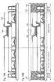
- Another structure of the present invention is a light emitting device comprising a light emitting element interposed between a pair of substrates, at least one of which is light transmitting, wherein the light emitting element is formed to be in contact with an interlayer insulating film, a side edge portion of the interlayer insulating film formed inside not to reach an edge portion of the substrate is processed into a tapered shape, an impermeable protective film is formed in the side edge portion of the interlayer insulating film, and the pair of substrates is fixed to each other with an impermeable composition in a region of the side edge portion of the interlayer insulating film or in an outer side of the region.
- Another structure of the present invention is a light emitting device according to the above structure, wherein a semiconductor film is formed from a bottom portion of the interlayer insulating film to the edge portion of the substrate.
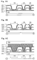
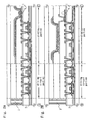
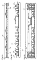
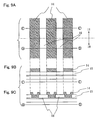
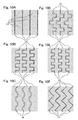
- the sealant 107 made of an impermeable material is formed on an outer side of the end face of the interlayer insulating film covered with the protective film or is formed to cover the entire end face of the interlayer insulating film in fixing the opposing substrate 108, water entry can further be prevented. Therefore, improvement in reliability can be expected.
- Embodiment Modes 2 and 3 it is a very effective means of preventing water entry to remove an interlayer insulating film on the periphery of a substrate and not to expose an end face of an interlayer insulating film to outer air as much as possible by covering the end face of the interlayer insulating film with a protective film 103 (and 105) and a sealant 107.
- a protective film 103 and 105
- a sealant 107 there may be a case that it is difficult to remove an entire interlayer insulating film, depending on a structure.
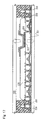
- FIGS. 10C to 10F show examples of other conceivable structures for realizing this embodiment mode.
- length of the interlayer insulating film between wirings gets longer even a little than the conventional structure in FIG. 10A, water entry can further be delayed than ever before.
- a desired pattern may be formed depending on necessity.
- a thin film of a nickel solution is formed on the surface of the semiconductor film by applying with a spinner a nickel acetate solution or a nickel nitrate solution containing nickel in a concentration of from 5 ppm to 10 ppm in terms of weight.
- the nickel element may be sprayed on the whole surface of the semiconductor film by sputtering instead of application.
- a catalytic element one of or a plurality of elements such as iron (Fe), palladium (Pd), tin (Sn), lead (Pb), cobalt (Co), platinum (Pt), copper (Cu), and gold (Au) may be used as well as nickel (Ni).
- the fourth impurity region (P + region) and the fifth impurity region (P - region) are formed by once third doping; however, the invention is not exclusively limited to this.
- the fourth impurity region (P + region) and the fifth impurity region (P - region) may be formed by multiple doping treatments according to each condition.
- evaporation is performed with an evaporation source moving by using an evaporation apparatus.
- evaporation is performed in a film formation chamber which is vacuum evacuated to 5 x 10 -3 Torr (0.665 Pa) or less, preferably to from 10 -4 Torr to 10 -6 Torr.
- an organic compound is previously vaporized by resistance heating and flies in a direction of the substrate when a shutter is opened in evaporation.
- the vaporized organic compound flies upwardly and is evaporated to the substrate through an opening provided for a metal mask to form a light emitting layer 244 (including a hole transport layer, a hole injection layer, an electron transport layer, and an electron injection layer).
- a shift register 500 In a row where a gate signal line is selected, a shift register 500 (SR) outputs a sampling pulse sequentially from a first stage in accordance with a clock pulse 504 and a start pulse 505.
- a first latch circuit 501 takes in a video signal in timing with a sampling pulse being inputted, and the video signal taken in at each stage is stored in the first latch circuit 501.
Landscapes
- Engineering & Computer Science (AREA)
- Microelectronics & Electronic Packaging (AREA)
- Physics & Mathematics (AREA)
- Spectroscopy & Molecular Physics (AREA)
- Chemical & Material Sciences (AREA)
- Materials Engineering (AREA)
- Geometry (AREA)
- Optics & Photonics (AREA)
- Electroluminescent Light Sources (AREA)
- Devices For Indicating Variable Information By Combining Individual Elements (AREA)
Applications Claiming Priority (4)
| Application Number | Priority Date | Filing Date | Title |
|---|---|---|---|
| JP2003347601 | 2003-08-29 | ||
| JP2003347601 | 2003-08-29 | ||
| JP2003322334 | 2003-09-12 | ||
| JP2003322334 | 2003-09-12 |
Publications (3)
| Publication Number | Publication Date |
|---|---|
| EP1511081A2 true EP1511081A2 (de) | 2005-03-02 |
| EP1511081A3 EP1511081A3 (de) | 2010-03-03 |
| EP1511081B1 EP1511081B1 (de) | 2019-10-09 |
Family
ID=34106978
Family Applications (1)
| Application Number | Title | Priority Date | Filing Date |
|---|---|---|---|
| EP04019744.4A Expired - Lifetime EP1511081B1 (de) | 2003-08-29 | 2004-08-19 | Lichtemittierende Vorrichtung |
Country Status (5)
| Country | Link |
|---|---|
| US (5) | US7928654B2 (de) |
| EP (1) | EP1511081B1 (de) |
| KR (2) | KR101158830B1 (de) |
| CN (2) | CN101483186B (de) |
| TW (6) | TWI501690B (de) |
Cited By (6)
| Publication number | Priority date | Publication date | Assignee | Title |
|---|---|---|---|---|
| EP1601031A1 (de) * | 2004-05-28 | 2005-11-30 | Samsung SDI Co., Ltd. | Organisches lichtemittierendes Bauelement und dessen Herstellung |
| EP2105964A1 (de) | 2008-02-28 | 2009-09-30 | Samsung Mobile Display Co., Ltd. | Organische lichtemittierende Anzeigevorrichtung |
| EP1814183A3 (de) * | 2006-01-26 | 2011-05-25 | Samsung Mobile Display Co., Ltd. | Organische lichtemittierende Anzeigevorrichtung |
| EP2267780A3 (de) * | 2009-06-26 | 2014-03-26 | Mitsubishi Electric Corporation | Bildanzeigevorrichtung und Herstellungsverfahren dafür |
| EP2267779A3 (de) * | 2009-06-26 | 2014-03-26 | Mitsubishi Electric Corporation | Bildanzeigevorrichtung und Herstellungsverfahren dafür |
| US11372276B2 (en) | 2014-11-26 | 2022-06-28 | Semiconductor Energy Laboratory Co., Ltd. | Display device and electronic device |
Families Citing this family (62)
| Publication number | Priority date | Publication date | Assignee | Title |
|---|---|---|---|---|
| SG142140A1 (en) * | 2003-06-27 | 2008-05-28 | Semiconductor Energy Lab | Display device and method of manufacturing thereof |
| US7928654B2 (en) | 2003-08-29 | 2011-04-19 | Semiconductor Energy Laboratory Co., Ltd. | Display device and method for manufacturing the same |
| JP4741177B2 (ja) * | 2003-08-29 | 2011-08-03 | 株式会社半導体エネルギー研究所 | 表示装置の作製方法 |
| KR100561646B1 (ko) * | 2003-10-23 | 2006-03-20 | 엘지.필립스 엘시디 주식회사 | 표시 소자용 박막 트랜지스터 기판 및 그 제조 방법 |
| US7619258B2 (en) * | 2004-03-16 | 2009-11-17 | Semiconductor Energy Laboratory Co., Ltd. | Display device |
| US7183147B2 (en) * | 2004-03-25 | 2007-02-27 | Semiconductor Energy Laboratory Co., Ltd. | Light emitting device, method for manufacturing thereof and electronic appliance |
| KR100681022B1 (ko) * | 2004-06-16 | 2007-02-09 | 엘지전자 주식회사 | 유기 전계발광표시소자 및 그 제조방법 |
| US8148895B2 (en) | 2004-10-01 | 2012-04-03 | Semiconductor Energy Laboratory Co., Ltd. | Display device and manufacturing method of the same |
| ATE476757T1 (de) * | 2004-10-21 | 2010-08-15 | Lg Display Co Ltd | Organische elektrolumineszente vorrichtung und herstellungsverfahren |
| JP4870933B2 (ja) * | 2005-03-04 | 2012-02-08 | 東北パイオニア株式会社 | 自発光パネルおよび自発光パネルの製造方法 |
| US20060214564A1 (en) * | 2005-03-24 | 2006-09-28 | Hsi-Ming Chang | Organic electroluminescent display and method for fabricating the same |
| KR100645533B1 (ko) * | 2005-05-27 | 2006-11-14 | 삼성에스디아이 주식회사 | 유기전계발광표시소자 및 그의 제조 방법 |
| KR101147991B1 (ko) * | 2005-06-23 | 2012-05-25 | 엘지디스플레이 주식회사 | 액정표시자치용 어레이 기판과 그 제조방법 |
| KR100695169B1 (ko) * | 2006-01-11 | 2007-03-14 | 삼성전자주식회사 | 평판표시장치 |
| KR100673765B1 (ko) * | 2006-01-20 | 2007-01-24 | 삼성에스디아이 주식회사 | 유기전계발광 표시장치 및 그 제조방법 |
| KR100635514B1 (ko) * | 2006-01-23 | 2006-10-18 | 삼성에스디아이 주식회사 | 유기전계발광표시장치 및 그 제조방법 |
| KR100671647B1 (ko) * | 2006-01-26 | 2007-01-19 | 삼성에스디아이 주식회사 | 유기전계발광 표시 장치 |
| JP5207670B2 (ja) * | 2006-07-19 | 2013-06-12 | キヤノン株式会社 | 表示装置 |
| TWI367565B (en) * | 2008-02-05 | 2012-07-01 | Chimei Innolux Corp | Double-layered active area structure with a polysilicon layer and a microcrystalline silicon layer, method for manufactruing the same and its application |
| JP2010257957A (ja) * | 2009-04-01 | 2010-11-11 | Seiko Epson Corp | 有機エレクトロルミネッセンス装置 |
| US8766269B2 (en) | 2009-07-02 | 2014-07-01 | Semiconductor Energy Laboratory Co., Ltd. | Light-emitting device, lighting device, and electronic device |
| TWI589042B (zh) * | 2010-01-20 | 2017-06-21 | 半導體能源研究所股份有限公司 | 發光裝置,撓性發光裝置,電子裝置,照明設備,以及發光裝置和撓性發光裝置的製造方法 |
| US9000442B2 (en) * | 2010-01-20 | 2015-04-07 | Semiconductor Energy Laboratory Co., Ltd. | Light-emitting device, flexible light-emitting device, electronic device, and method for manufacturing light-emitting device and flexible-light emitting device |
| US20120074434A1 (en) * | 2010-09-24 | 2012-03-29 | Jun Seok Park | Light emitting device package and lighting apparatus using the same |
| KR101223724B1 (ko) * | 2010-10-25 | 2013-01-17 | 삼성디스플레이 주식회사 | 전자소자용 보호막 및 그 제조 방법 |
| KR20130025717A (ko) * | 2011-09-02 | 2013-03-12 | 삼성디스플레이 주식회사 | 유기 발광 표시 장치 및 유기 발광 표시 장치 제조 방법 |
| KR101876540B1 (ko) * | 2011-12-28 | 2018-07-10 | 삼성디스플레이 주식회사 | 가요성 표시 장치 및 가요성 표시 장치의 제조 방법 |
| WO2013136771A1 (ja) | 2012-03-12 | 2013-09-19 | パナソニック株式会社 | 有機エレクトロルミネッセンス素子 |
| JP6073890B2 (ja) * | 2012-07-26 | 2017-02-01 | パナソニック株式会社 | 有機el装置 |
| US12302698B2 (en) | 2012-07-31 | 2025-05-13 | Jdi Design And Development G.K. | Display unit with moisture proof film outside of seal section and electronic apparatus with said display unit |
| JP6142151B2 (ja) * | 2012-07-31 | 2017-06-07 | 株式会社Joled | 表示装置および電子機器 |
| KR101965257B1 (ko) * | 2012-10-08 | 2019-04-04 | 삼성디스플레이 주식회사 | 플렉시블 표시 장치 |
| KR102047729B1 (ko) * | 2013-04-30 | 2019-11-22 | 엘지디스플레이 주식회사 | 유기전계발광표시장치 및 그 제조방법 |
| KR102153394B1 (ko) | 2013-07-29 | 2020-09-08 | 엘지디스플레이 주식회사 | 유기발광 표시장치 |
| JP6234898B2 (ja) * | 2013-09-25 | 2017-11-22 | 信越化学工業株式会社 | フォトマスクブランクの製造方法 |
| KR102114316B1 (ko) * | 2013-10-02 | 2020-05-25 | 삼성디스플레이 주식회사 | 유기발광 디스플레이 장치 및 그 제조방법 |
| KR102116896B1 (ko) * | 2013-10-14 | 2020-06-01 | 삼성디스플레이 주식회사 | 유기 발광 표시 장치 |
| KR102117109B1 (ko) * | 2013-10-22 | 2020-06-01 | 삼성디스플레이 주식회사 | 유기 발광 표시 장치 |
| KR102216672B1 (ko) * | 2013-10-22 | 2021-02-18 | 삼성디스플레이 주식회사 | 유기 발광 표시 장치 및 그 제조 방법 |
| KR102159149B1 (ko) * | 2013-12-23 | 2020-09-24 | 삼성디스플레이 주식회사 | 유기 발광 표시 장치용 원장 기판 및 유기 발광 표시 장치의 제조 방법 |
| KR102085961B1 (ko) * | 2013-12-24 | 2020-03-06 | 엘지디스플레이 주식회사 | 플렉서블 유기 발광 표시 장치 및 플렉서블 유기 발광 표시 장치 제조 방법 |
| KR102360783B1 (ko) * | 2014-09-16 | 2022-02-10 | 삼성디스플레이 주식회사 | 디스플레이 장치 |
| KR102284756B1 (ko) | 2014-09-23 | 2021-08-03 | 삼성디스플레이 주식회사 | 디스플레이 장치 |
| US9991326B2 (en) * | 2015-01-14 | 2018-06-05 | Panasonic Intellectual Property Management Co., Ltd. | Light-emitting device comprising flexible substrate and light-emitting element |
| JP6608201B2 (ja) * | 2015-07-10 | 2019-11-20 | 株式会社ジャパンディスプレイ | 自発光表示装置 |
| KR102381285B1 (ko) * | 2015-08-06 | 2022-03-31 | 삼성디스플레이 주식회사 | 가요성 표시 장치 및 이의 제조 방법 |
| KR102430819B1 (ko) * | 2015-08-19 | 2022-08-10 | 삼성디스플레이 주식회사 | 유기 발광 표시 장치 및 유기 발광 표시 장치의 제조 방법 |
| KR102427249B1 (ko) | 2015-10-16 | 2022-08-01 | 삼성디스플레이 주식회사 | 디스플레이 장치 |
| JP2017168308A (ja) * | 2016-03-16 | 2017-09-21 | 株式会社Joled | 表示装置 |
| KR102550322B1 (ko) * | 2016-03-22 | 2023-07-03 | 삼성디스플레이 주식회사 | 표시 장치 및 그 제조 방법 |
| KR102628849B1 (ko) * | 2016-03-24 | 2024-01-25 | 삼성디스플레이 주식회사 | 유기발광 디스플레이 장치 |
| KR102559837B1 (ko) * | 2016-06-02 | 2023-07-27 | 삼성디스플레이 주식회사 | 디스플레이 장치 |
| US20180040638A1 (en) * | 2016-08-05 | 2018-02-08 | Innolux Corporation | Display device |
| KR102553910B1 (ko) | 2016-08-31 | 2023-07-07 | 엘지디스플레이 주식회사 | 표시장치와 그의 검사방법 |
| KR102806394B1 (ko) * | 2016-09-28 | 2025-05-13 | 삼성디스플레이 주식회사 | 디스플레이 장치 |
| KR102479020B1 (ko) * | 2017-11-28 | 2022-12-19 | 삼성디스플레이 주식회사 | 표시 장치 |
| KR102520016B1 (ko) * | 2018-02-02 | 2023-04-11 | 삼성디스플레이 주식회사 | 표시 패널 및 이를 포함하는 전자 장치 |
| TWI697810B (zh) | 2018-05-10 | 2020-07-01 | 宏碁股份有限公司 | 具備手勢感測功能之三維顯示器 |
| CN109243305B (zh) * | 2018-09-17 | 2021-10-12 | 京东方科技集团股份有限公司 | 显示面板、显示装置和显示面板的制造方法 |
| CN111370439A (zh) | 2018-12-07 | 2020-07-03 | 京东方科技集团股份有限公司 | 显示面板及其制备方法、显示装置 |
| KR102656092B1 (ko) * | 2019-07-15 | 2024-04-11 | 삼성디스플레이 주식회사 | 표시 장치 및 이의 제조 방법 |
| KR102763278B1 (ko) * | 2019-12-31 | 2025-02-10 | 삼성디스플레이 주식회사 | 표시 패널 |
Family Cites Families (59)
| Publication number | Priority date | Publication date | Assignee | Title |
|---|---|---|---|---|
| JPH05299177A (ja) | 1992-04-22 | 1993-11-12 | Sharp Corp | 薄膜エレクトロ・ルミネッセンス素子 |
| US6723811B1 (en) | 1994-12-28 | 2004-04-20 | Cambridge Display Technology Ltd. | Polymers for use in optical device |
| JPH09148066A (ja) | 1995-11-24 | 1997-06-06 | Pioneer Electron Corp | 有機el素子 |
| TW477907B (en) | 1997-03-07 | 2002-03-01 | Toshiba Corp | Array substrate, liquid crystal display device and their manufacturing method |
| JP3774897B2 (ja) | 1997-06-03 | 2006-05-17 | ソニー株式会社 | 有機電界発光素子 |
| US6303238B1 (en) | 1997-12-01 | 2001-10-16 | The Trustees Of Princeton University | OLEDs doped with phosphorescent compounds |
| US6413656B1 (en) | 1998-09-14 | 2002-07-02 | The University Of Southern California | Reduced symmetry porphyrin molecules for producing enhanced luminosity from phosphorescent organic light emitting devices |
| US6420031B1 (en) | 1997-11-03 | 2002-07-16 | The Trustees Of Princeton University | Highly transparent non-metallic cathodes |
| US6150043A (en) | 1998-04-10 | 2000-11-21 | The Trustees Of Princeton University | OLEDs containing thermally stable glassy organic hole transporting materials |
| US6451455B1 (en) | 1998-04-01 | 2002-09-17 | The Trustees Of Princeton University | Metal complexes bearing both electron transporting and hole transporting moieties |
| US6469437B1 (en) | 1997-11-03 | 2002-10-22 | The Trustees Of Princeton University | Highly transparent organic light emitting device employing a non-metallic cathode |
| WO1999020081A2 (en) | 1997-10-09 | 1999-04-22 | The Trustees Of Princeton University | Highly transparent non-metallic cathodes |
| US6030715A (en) | 1997-10-09 | 2000-02-29 | The University Of Southern California | Azlactone-related dopants in the emissive layer of an OLED |
| TW476227B (en) * | 1997-10-09 | 2002-02-11 | Univ Princeton | Optoelectronic devices containing highly transparent non-metallic cathodes |
| JPH11202349A (ja) | 1998-01-12 | 1999-07-30 | Semiconductor Energy Lab Co Ltd | 表示装置 |
| JP3646510B2 (ja) | 1998-03-18 | 2005-05-11 | セイコーエプソン株式会社 | 薄膜形成方法、表示装置およびカラーフィルタ |
| US6387544B1 (en) | 1998-04-10 | 2002-05-14 | The Trustees Of Princeton University | OLEDS containing thermally stable glassy organic hole transporting materials |
| JP3883706B2 (ja) * | 1998-07-31 | 2007-02-21 | シャープ株式会社 | エッチング方法、及び薄膜トランジスタマトリックス基板の製造方法 |
| JP2000173766A (ja) * | 1998-09-30 | 2000-06-23 | Sanyo Electric Co Ltd | 表示装置 |
| US7288420B1 (en) | 1999-06-04 | 2007-10-30 | Semiconductor Energy Laboratory Co., Ltd. | Method for manufacturing an electro-optical device |
| KR100335462B1 (ko) * | 1999-08-11 | 2002-05-04 | 구본준, 론 위라하디락사 | 액정표시패널 |
| US7112115B1 (en) | 1999-11-09 | 2006-09-26 | Semiconductor Energy Laboratory Co., Ltd. | Light emitting device and method of manufacturing the same |
| US6633121B2 (en) | 2000-01-31 | 2003-10-14 | Idemitsu Kosan Co., Ltd. | Organic electroluminescence display device and method of manufacturing same |
| AU3483001A (en) | 2000-02-04 | 2001-08-14 | Corixa Corp | Compositions and methods for the therapy and diagnosis of ovarian cancer |
| TW525305B (en) | 2000-02-22 | 2003-03-21 | Semiconductor Energy Lab | Self-light-emitting device and method of manufacturing the same |
| TW521237B (en) * | 2000-04-18 | 2003-02-21 | Semiconductor Energy Lab | Light emitting device |
| JP2001357973A (ja) | 2000-06-15 | 2001-12-26 | Sony Corp | 表示装置 |
| US7019718B2 (en) | 2000-07-25 | 2006-03-28 | Semiconductor Energy Laboratory Co., Ltd. | Display device |
| US7223643B2 (en) * | 2000-08-11 | 2007-05-29 | Semiconductor Energy Laboratory Co., Ltd. | Method of manufacturing a semiconductor device |
| JP3480444B2 (ja) * | 2000-12-26 | 2003-12-22 | 日本電気株式会社 | Gfpフレーム転送装置およびgfpフレーム転送方法 |
| SG102681A1 (en) | 2001-02-19 | 2004-03-26 | Semiconductor Energy Lab | Light emitting device and method of manufacturing the same |
| US6992439B2 (en) * | 2001-02-22 | 2006-01-31 | Semiconductor Energy Laboratory Co., Ltd. | Display device with sealing structure for protecting organic light emitting element |
| JP4801278B2 (ja) | 2001-04-23 | 2011-10-26 | 株式会社半導体エネルギー研究所 | 発光装置及びその作製方法 |
| US6952023B2 (en) | 2001-07-17 | 2005-10-04 | Semiconductor Energy Laboratory Co., Ltd. | Light emitting device |
| US7488986B2 (en) * | 2001-10-26 | 2009-02-10 | Semiconductor Energy Laboratory Co., Ltd. | Light emitting device |
| CN100380673C (zh) | 2001-11-09 | 2008-04-09 | 株式会社半导体能源研究所 | 发光设备及其制造方法 |
| US7042024B2 (en) | 2001-11-09 | 2006-05-09 | Semiconductor Energy Laboratory Co., Ltd. | Light emitting apparatus and method for manufacturing the same |
| JP4515022B2 (ja) | 2001-11-16 | 2010-07-28 | 株式会社半導体エネルギー研究所 | 発光装置 |
| US6822264B2 (en) * | 2001-11-16 | 2004-11-23 | Semiconductor Energy Laboratory Co., Ltd. | Light emitting device |
| JP4101511B2 (ja) | 2001-12-27 | 2008-06-18 | 株式会社半導体エネルギー研究所 | 発光装置及びその作製方法 |
| CN1184995C (zh) | 2002-01-08 | 2005-01-19 | 郑国升 | 强肾助孕冲剂 |
| EP1492387A1 (de) | 2002-03-29 | 2004-12-29 | Pioneer Corporation | Organische elektrolumineszenzanzeigetafel |
| JP2003297552A (ja) | 2002-03-29 | 2003-10-17 | Pioneer Electronic Corp | 有機エレクトロルミネッセンス表示パネル |
| JP3989763B2 (ja) * | 2002-04-15 | 2007-10-10 | 株式会社半導体エネルギー研究所 | 半導体表示装置 |
| US7221093B2 (en) * | 2002-06-10 | 2007-05-22 | Institute Of Materials Research And Engineering | Patterning of electrodes in OLED devices |
| AU2003288999A1 (en) | 2002-12-19 | 2004-07-14 | Semiconductor Energy Laboratory Co., Ltd. | Display unit and method of fabricating display unit |
| KR100675630B1 (ko) * | 2002-12-31 | 2007-02-01 | 엘지.필립스 엘시디 주식회사 | 액정 표시패널 및 그 제조방법 |
| KR100972148B1 (ko) * | 2002-12-31 | 2010-07-23 | 엘지디스플레이 주식회사 | 씰패턴 하부의 적층구조에 특징을 가지는 액정표시장치 |
| JP4417027B2 (ja) | 2003-05-21 | 2010-02-17 | 株式会社半導体エネルギー研究所 | 発光装置 |
| SG142140A1 (en) | 2003-06-27 | 2008-05-28 | Semiconductor Energy Lab | Display device and method of manufacturing thereof |
| US7928654B2 (en) * | 2003-08-29 | 2011-04-19 | Semiconductor Energy Laboratory Co., Ltd. | Display device and method for manufacturing the same |
| JP4741177B2 (ja) | 2003-08-29 | 2011-08-03 | 株式会社半導体エネルギー研究所 | 表示装置の作製方法 |
| US7619258B2 (en) | 2004-03-16 | 2009-11-17 | Semiconductor Energy Laboratory Co., Ltd. | Display device |
| CN1819300B (zh) * | 2004-09-17 | 2010-06-16 | 株式会社半导体能源研究所 | 发光器件 |
| KR100635514B1 (ko) * | 2006-01-23 | 2006-10-18 | 삼성에스디아이 주식회사 | 유기전계발광표시장치 및 그 제조방법 |
| JP5299177B2 (ja) | 2009-09-01 | 2013-09-25 | トヨタ自動車株式会社 | 内燃機関の燃焼制御装置 |
| KR20150033195A (ko) * | 2013-09-23 | 2015-04-01 | 삼성디스플레이 주식회사 | 유기 발광 표시 장치 및 그 제조 방법 |
| KR102160813B1 (ko) * | 2014-01-07 | 2020-09-29 | 삼성디스플레이 주식회사 | 유기 발광 표시장치 및 그의 제조방법 |
| KR102264651B1 (ko) * | 2015-02-03 | 2021-06-15 | 삼성디스플레이 주식회사 | 표시 장치 및 그 제조 방법 |
-
2004
- 2004-08-17 US US10/919,605 patent/US7928654B2/en not_active Expired - Lifetime
- 2004-08-19 TW TW101139484A patent/TWI501690B/zh not_active IP Right Cessation
- 2004-08-19 TW TW107100086A patent/TWI674034B/zh not_active IP Right Cessation
- 2004-08-19 EP EP04019744.4A patent/EP1511081B1/de not_active Expired - Lifetime
- 2004-08-19 TW TW105135726A patent/TWI619405B/zh not_active IP Right Cessation
- 2004-08-19 TW TW093125022A patent/TWI407825B/zh not_active IP Right Cessation
- 2004-08-19 TW TW108126146A patent/TWI748211B/zh not_active IP Right Cessation
- 2004-08-19 TW TW104121146A patent/TWI571168B/zh not_active IP Right Cessation
- 2004-08-27 CN CN2008101863347A patent/CN101483186B/zh not_active Expired - Fee Related
- 2004-08-27 CN CNB2004100822835A patent/CN100459184C/zh not_active Expired - Fee Related
- 2004-08-30 KR KR1020040068372A patent/KR101158830B1/ko not_active Expired - Fee Related
-
2011
- 2011-04-18 US US13/088,578 patent/US8723417B2/en not_active Expired - Lifetime
-
2012
- 2012-01-27 KR KR1020120008323A patent/KR101260294B1/ko not_active Expired - Fee Related
-
2014
- 2014-05-09 US US14/274,143 patent/US9923127B2/en not_active Expired - Fee Related
-
2018
- 2018-03-13 US US15/919,780 patent/US10367124B2/en not_active Expired - Lifetime
-
2019
- 2019-07-25 US US16/522,202 patent/US10903402B2/en not_active Expired - Fee Related
Cited By (11)
| Publication number | Priority date | Publication date | Assignee | Title |
|---|---|---|---|---|
| EP1601031A1 (de) * | 2004-05-28 | 2005-11-30 | Samsung SDI Co., Ltd. | Organisches lichtemittierendes Bauelement und dessen Herstellung |
| US7579767B2 (en) | 2004-05-28 | 2009-08-25 | Samsung Mobile Display Co., Ltd. | Organic light emitting device having triple layered pixel electrode |
| US8183063B2 (en) | 2004-05-28 | 2012-05-22 | Samsung Mobile Display Co., Ltd. | Organic light emitting device and method of fabricating the same |
| EP1814183A3 (de) * | 2006-01-26 | 2011-05-25 | Samsung Mobile Display Co., Ltd. | Organische lichtemittierende Anzeigevorrichtung |
| EP2105964A1 (de) | 2008-02-28 | 2009-09-30 | Samsung Mobile Display Co., Ltd. | Organische lichtemittierende Anzeigevorrichtung |
| US8049412B2 (en) | 2008-02-28 | 2011-11-01 | Samsung Mobile Display Co., Ltd. | Organic light emitting display device |
| EP2267780A3 (de) * | 2009-06-26 | 2014-03-26 | Mitsubishi Electric Corporation | Bildanzeigevorrichtung und Herstellungsverfahren dafür |
| EP2267779A3 (de) * | 2009-06-26 | 2014-03-26 | Mitsubishi Electric Corporation | Bildanzeigevorrichtung und Herstellungsverfahren dafür |
| US11372276B2 (en) | 2014-11-26 | 2022-06-28 | Semiconductor Energy Laboratory Co., Ltd. | Display device and electronic device |
| US11635648B2 (en) | 2014-11-26 | 2023-04-25 | Semiconductor Energy Laboratory Co., Ltd. | Display device and electronic device |
| US12153298B2 (en) | 2014-11-26 | 2024-11-26 | Semiconductor Energy Laboratory Co., Ltd. | Display device and electronic device |
Also Published As
| Publication number | Publication date |
|---|---|
| US20200020835A1 (en) | 2020-01-16 |
| US7928654B2 (en) | 2011-04-19 |
| CN101483186B (zh) | 2013-04-03 |
| TW202014050A (zh) | 2020-04-01 |
| TW201724909A (zh) | 2017-07-01 |
| CN1655370A (zh) | 2005-08-17 |
| US10903402B2 (en) | 2021-01-26 |
| TWI619405B (zh) | 2018-03-21 |
| KR101260294B1 (ko) | 2013-05-03 |
| CN101483186A (zh) | 2009-07-15 |
| TWI748211B (zh) | 2021-12-01 |
| TW201831046A (zh) | 2018-08-16 |
| KR20050021963A (ko) | 2005-03-07 |
| EP1511081B1 (de) | 2019-10-09 |
| US20050046346A1 (en) | 2005-03-03 |
| TWI571168B (zh) | 2017-02-11 |
| TW201309082A (zh) | 2013-02-16 |
| US10367124B2 (en) | 2019-07-30 |
| US20180204988A1 (en) | 2018-07-19 |
| US20140246694A1 (en) | 2014-09-04 |
| TWI674034B (zh) | 2019-10-01 |
| US9923127B2 (en) | 2018-03-20 |
| US8723417B2 (en) | 2014-05-13 |
| TWI501690B (zh) | 2015-09-21 |
| US20110248313A1 (en) | 2011-10-13 |
| TW200518616A (en) | 2005-06-01 |
| CN100459184C (zh) | 2009-02-04 |
| TWI407825B (zh) | 2013-09-01 |
| EP1511081A3 (de) | 2010-03-03 |
| KR20120034687A (ko) | 2012-04-12 |
| TW201601586A (zh) | 2016-01-01 |
| KR101158830B1 (ko) | 2012-06-27 |
Similar Documents
| Publication | Publication Date | Title |
|---|---|---|
| US10903402B2 (en) | Display device and method for manufacturing the same | |
| JP6691190B2 (ja) | 発光装置 | |
| JP4519532B2 (ja) | 発光装置及び発光装置を用いた電子機器 | |
| JP4683883B2 (ja) | 発光装置 | |
| JP4694429B2 (ja) | 半導体装置の作製方法 |
Legal Events
| Date | Code | Title | Description |
|---|---|---|---|
| PUAI | Public reference made under article 153(3) epc to a published international application that has entered the european phase |
Free format text: ORIGINAL CODE: 0009012 |
|
| AK | Designated contracting states |
Kind code of ref document: A2 Designated state(s): AT BE BG CH CY CZ DE DK EE ES FI FR GB GR HU IE IT LI LU MC NL PL PT RO SE SI SK TR |
|
| AX | Request for extension of the european patent |
Extension state: AL HR LT LV MK |
|
| 17P | Request for examination filed |
Effective date: 20050901 |
|
| RIC1 | Information provided on ipc code assigned before grant |
Ipc: H01L 27/32 20060101AFI20091110BHEP Ipc: H01L 51/52 20060101ALI20091110BHEP |
|
| PUAL | Search report despatched |
Free format text: ORIGINAL CODE: 0009013 |
|
| AK | Designated contracting states |
Kind code of ref document: A3 Designated state(s): AT BE BG CH CY CZ DE DK EE ES FI FR GB GR HU IE IT LI LU MC NL PL PT RO SE SI SK TR |
|
| AX | Request for extension of the european patent |
Extension state: AL HR LT LV MK |
|
| AKX | Designation fees paid |
Designated state(s): DE FI FR GB NL |
|
| 17Q | First examination report despatched |
Effective date: 20170308 |
|
| GRAP | Despatch of communication of intention to grant a patent |
Free format text: ORIGINAL CODE: EPIDOSNIGR1 |
|
| INTG | Intention to grant announced |
Effective date: 20190520 |
|
| GRAS | Grant fee paid |
Free format text: ORIGINAL CODE: EPIDOSNIGR3 |
|
| GRAA | (expected) grant |
Free format text: ORIGINAL CODE: 0009210 |
|
| AK | Designated contracting states |
Kind code of ref document: B1 Designated state(s): DE FI FR GB NL |
|
| REG | Reference to a national code |
Ref country code: GB Ref legal event code: FG4D |
|
| REG | Reference to a national code |
Ref country code: DE Ref legal event code: R096 Ref document number: 602004054286 Country of ref document: DE |
|
| REG | Reference to a national code |
Ref country code: NL Ref legal event code: MP Effective date: 20191009 |
|
| PG25 | Lapsed in a contracting state [announced via postgrant information from national office to epo] |
Ref country code: NL Free format text: LAPSE BECAUSE OF FAILURE TO SUBMIT A TRANSLATION OF THE DESCRIPTION OR TO PAY THE FEE WITHIN THE PRESCRIBED TIME-LIMIT Effective date: 20191009 Ref country code: FI Free format text: LAPSE BECAUSE OF FAILURE TO SUBMIT A TRANSLATION OF THE DESCRIPTION OR TO PAY THE FEE WITHIN THE PRESCRIBED TIME-LIMIT Effective date: 20191009 |
|
| REG | Reference to a national code |
Ref country code: DE Ref legal event code: R097 Ref document number: 602004054286 Country of ref document: DE |
|
| PLBE | No opposition filed within time limit |
Free format text: ORIGINAL CODE: 0009261 |
|
| STAA | Information on the status of an ep patent application or granted ep patent |
Free format text: STATUS: NO OPPOSITION FILED WITHIN TIME LIMIT |
|
| 26N | No opposition filed |
Effective date: 20200710 |
|
| GBPC | Gb: european patent ceased through non-payment of renewal fee |
Effective date: 20200819 |
|
| PG25 | Lapsed in a contracting state [announced via postgrant information from national office to epo] |
Ref country code: FR Free format text: LAPSE BECAUSE OF NON-PAYMENT OF DUE FEES Effective date: 20200831 |
|
| PG25 | Lapsed in a contracting state [announced via postgrant information from national office to epo] |
Ref country code: GB Free format text: LAPSE BECAUSE OF NON-PAYMENT OF DUE FEES Effective date: 20200819 |
|
| PGFP | Annual fee paid to national office [announced via postgrant information from national office to epo] |
Ref country code: DE Payment date: 20220608 Year of fee payment: 19 |
|
| REG | Reference to a national code |
Ref country code: DE Ref legal event code: R079 Ref document number: 602004054286 Country of ref document: DE Free format text: PREVIOUS MAIN CLASS: H01L0027320000 Ipc: H10K0059000000 |
|
| REG | Reference to a national code |
Ref country code: DE Ref legal event code: R119 Ref document number: 602004054286 Country of ref document: DE |
|
| PG25 | Lapsed in a contracting state [announced via postgrant information from national office to epo] |
Ref country code: DE Free format text: LAPSE BECAUSE OF NON-PAYMENT OF DUE FEES Effective date: 20240301 |