EP1601031A1 - Organisches lichtemittierendes Bauelement und dessen Herstellung - Google Patents
Organisches lichtemittierendes Bauelement und dessen Herstellung Download PDFInfo
- Publication number
- EP1601031A1 EP1601031A1 EP05104334A EP05104334A EP1601031A1 EP 1601031 A1 EP1601031 A1 EP 1601031A1 EP 05104334 A EP05104334 A EP 05104334A EP 05104334 A EP05104334 A EP 05104334A EP 1601031 A1 EP1601031 A1 EP 1601031A1
- Authority
- EP
- European Patent Office
- Prior art keywords
- pixel electrode
- layer
- light emitting
- emitting device
- organic light
- Prior art date
- Legal status (The legal status is an assumption and is not a legal conclusion. Google has not performed a legal analysis and makes no representation as to the accuracy of the status listed.)
- Withdrawn
Links
Images


Classifications
-
- H—ELECTRICITY
- H05—ELECTRIC TECHNIQUES NOT OTHERWISE PROVIDED FOR
- H05B—ELECTRIC HEATING; ELECTRIC LIGHT SOURCES NOT OTHERWISE PROVIDED FOR; CIRCUIT ARRANGEMENTS FOR ELECTRIC LIGHT SOURCES, IN GENERAL
- H05B33/00—Electroluminescent light sources
- H05B33/12—Light sources with substantially two-dimensional [2D] radiating surfaces
- H05B33/26—Light sources with substantially two-dimensional [2D] radiating surfaces characterised by the composition or arrangement of the conductive material used as an electrode
-
- H—ELECTRICITY
- H10—SEMICONDUCTOR DEVICES; ELECTRIC SOLID-STATE DEVICES NOT OTHERWISE PROVIDED FOR
- H10K—ORGANIC ELECTRIC SOLID-STATE DEVICES
- H10K59/00—Integrated devices, or assemblies of multiple devices, comprising at least one organic light-emitting element covered by group H10K50/00
- H10K59/80—Constructional details
- H10K59/875—Arrangements for extracting light from the devices
- H10K59/878—Arrangements for extracting light from the devices comprising reflective means
-
- H—ELECTRICITY
- H10—SEMICONDUCTOR DEVICES; ELECTRIC SOLID-STATE DEVICES NOT OTHERWISE PROVIDED FOR
- H10K—ORGANIC ELECTRIC SOLID-STATE DEVICES
- H10K50/00—Organic light-emitting devices
- H10K50/80—Constructional details
- H10K50/805—Electrodes
- H10K50/81—Anodes
- H10K50/818—Reflective anodes, e.g. ITO combined with thick metallic layers
-
- H—ELECTRICITY
- H10—SEMICONDUCTOR DEVICES; ELECTRIC SOLID-STATE DEVICES NOT OTHERWISE PROVIDED FOR
- H10K—ORGANIC ELECTRIC SOLID-STATE DEVICES
- H10K50/00—Organic light-emitting devices
- H10K50/80—Constructional details
- H10K50/85—Arrangements for extracting light from the devices
- H10K50/856—Arrangements for extracting light from the devices comprising reflective means
-
- H—ELECTRICITY
- H10—SEMICONDUCTOR DEVICES; ELECTRIC SOLID-STATE DEVICES NOT OTHERWISE PROVIDED FOR
- H10K—ORGANIC ELECTRIC SOLID-STATE DEVICES
- H10K2102/00—Constructional details relating to the organic devices covered by this subclass
- H10K2102/301—Details of OLEDs
- H10K2102/302—Details of OLEDs of OLED structures
- H10K2102/3023—Direction of light emission
- H10K2102/3026—Top emission
-
- H—ELECTRICITY
- H10—SEMICONDUCTOR DEVICES; ELECTRIC SOLID-STATE DEVICES NOT OTHERWISE PROVIDED FOR
- H10K—ORGANIC ELECTRIC SOLID-STATE DEVICES
- H10K2102/00—Constructional details relating to the organic devices covered by this subclass
- H10K2102/301—Details of OLEDs
- H10K2102/351—Thickness
-
- H—ELECTRICITY
- H10—SEMICONDUCTOR DEVICES; ELECTRIC SOLID-STATE DEVICES NOT OTHERWISE PROVIDED FOR
- H10K—ORGANIC ELECTRIC SOLID-STATE DEVICES
- H10K59/00—Integrated devices, or assemblies of multiple devices, comprising at least one organic light-emitting element covered by group H10K50/00
- H10K59/10—OLED displays
- H10K59/12—Active-matrix OLED [AMOLED] displays
- H10K59/122—Pixel-defining structures or layers, e.g. banks
Definitions
- the present invention relates to an organic light emitting device (OLED) and a method of fabricating the same and, more particularly, to an OLED and a method of fabricating the same, which includes a pixel electrode with a triple-layered structure, having a reflective layer made of Ag interposed, therein.
- OLED organic light emitting device
- an OLED is an emissive display device electrically exciting a fluorescent organic compound to emit light.
- the OLED is classified into a passive matrix OLED and an active matrix OLED depending on the type of driving N x M pixels.
- the active matrix OLED (AMOLED) is used with large screen displays and has high resolution. Further, the AMOLED consumes less power than the passive matrix OLED (PMOLED).
- the OLED is further classified into a top emission OLED, a bottom emission OLED, and a both sides emission OLED depending on the direction of light emitted from an organic compound.
- the both sides emission OLED simultaneously performs top and bottom emission.
- the top emission OLED i.e., a device for emitting light in an opposite direction of a substrate, at which unit pixels are disposed, has a higher aperture ratio than that of the bottom emission OLED.
- the both sides emission OLED including a main display window of the top emission OLED and an auxiliary display window of the bottom emission OLED is increasing.
- the both sides emission OLED is commonly used in mobile phones, which includes an auxiliary display window at an outer part and a main display window at an inner part.
- the auxiliary display window uses less power than the main display window to continuously maintain an "on" state when the mobile phone is in a standby state, thereby displaying, for example, a signal receiving state, a battery state of charge, current time, etc., of the mobile phone.
- FIG. 1A is a cross-sectional view of a conventional OLED.
- a buffer layer 110 of a predetermined thickness is formed on a substrate 100, and then a thin film transistor including a polysilicon pattern 122, a gate electrode 132, and source and drain electrodes 150 and 152 is formed.
- Source and drain regions 120, at which impurities are ion implanted, are provided at both sides of the polysilicon pattern 122, and a gate insulating layer 130 is disposed on an entire surface of the resultant structure.
- a passivation layer 160 of a predetermined thickness is then formed on the entire surface of the resultant structure, and the passivation layer 160 is etched by photolithography and etching processes to form a first via-contact hole (not shown) to expose one ofthe source and drain electrodes 150 and 152, for example, the drain electrode 152.
- the passivation layer 160 is an organic insulating layer formed of silicon nitride, silicon oxide, or a stacked structure thereof
- a first insulating layer 170 then formed on the entire surface of the resultant structure.
- the first insulating layer 170 may be formed of a material selected from a group consisting of polyimide, benzocyclobutene-based resin, spin on glass (SOG), acrylate, and the like, which is formed to planarize a pixel region.
- the first insulating layer 170 is etched by the photolithography and etching processes to form a second via-contact hole (not shown) to expose the first via-contact hole.
- a stacked structure of a reflective layer (not shown) and a thin layer for a pixel electrode (not shown) is then formed on the entire surface of the resultant structure.
- the reflective layer is formed of a highly reflective metal, such as Al, Mo, Ti, Au, Ag, Pd, or an alloy thereof
- the top emission OLED is formed, and when the reflective layer is formed according to the process described below, the bottom emission OLED is formed.
- the bottom emission OLED is formed with a thin layer for the pixel electrode having a thickness of approximately 10 ⁇ to - 300 ⁇ , using a transparent metal material, such as ITO (indium tin oxide).
- a transparent metal material such as ITO (indium tin oxide).
- the stacked structure is etched by the photolithography and etching processes to form a pixel electrode 182 and a reflective layer pattern 180a.
- a second insulating layer pattern 190 for defining an emission region is then formed on the entire surface of the resultant structure.
- the second insulating layer pattern 190 may be formed of one material selected from a group consisting of polyimide, benzocyclobutene-based resin, phenol resin, acrylate, and the like.
- An emission layer 192 is formed in the pixel region defined by the second insulating layer pattern 190 using a low molecule deposition method or a laser induced thermal imaging method.
- An opposite electrode (not shown) is formed to complete the OLED.
- the opposite electrode is formed of a transparent electrode or a transparent metal electrode
- the opposite electrode is formed of a metal electrode or a reflective electrode including a reflective layer.
- the reflective layer pattern 180a and the pixel electrode 182 are simultaneously exposed to an electrolyte solution used in the photolithography and etching processes, resulting in a galvanic phenomenon when a material having large electromotive force of the stacked structure is corroded, thereby damaging the pixel electrode.
- optical characteristics such as brightness, are deteriorated.
- FIG. 1B is a cross-sectional view of an OLED formed by another conventional process.
- a reflective layer pattern 180b is formed having an island structure.
- the reflective layer pattern 180b and the pixel electrode 182 may not be simultaneously exposed to the electrolyte solution used in the photolithography and etching processes.
- the reflective layer pattern is formed of Al
- the reflective layer pattern and the pixel electrode should be separately patterned.
- the top emission OLED uses a resonance effect oflight, it is important to allow color coordinates to be readily adjusted by forming the pixel electrode as thin as possible.
- a thin pixel electrode is formed a short circuit is likely to be generated at a step portion ofthe via-contact hole.
- the present invention therefore, solves aforementioned problems associated with conventional devices by providing an OLED and a method of fabricating the same capable of improving electrical characteristics and optical characteristics ofthe device by forming a stacked structure of a lower pixel electrode, a reflective layer pattern using Ag and an upper pixel electrode, as a pixel electrode.
- FIG. 1A is a cross-sectional view of an OLED formed by conventional operations.
- FIG. 1B is a cross-sectional view of an OLED formed by other conventional operations.
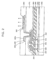
- FIG. 2 is a cross-sectional view of an OLED according to an embodiment of the invention.
- FIG. 3 is a graph showing reflectivity depending on a type of reflective layer.
- FIG. 4 is a graph showing reflectivity depending on a type of reflective layer and the thickness of a pixel electrode.
- FIG. 2 is a cross-sectional view of an OLED according to an embodiment of the invention, including a triple-layered pixel electrode having a lower pixel electrode 280a, a reflective layer pattern 282 and an upper pixel electrode 280b on a substrate 200.
- a triple-layered pixel electrode having a lower pixel electrode 280a, a reflective layer pattern 282 and an upper pixel electrode 280b on a substrate 200.
- the reflective layer pattern 282 may be formed of Ag.
- the organic light emitting display may be formed according to the following operations.
- a buffer layer 210 having a predetermined thickness is formed on an entire surface of a substrate 200 made of glass, quartz, sapphire, or the like.
- the buffer layer 210 may be formed of silicon oxide using a plasma-enhanced chemical vapor deposition (PECVD) method.
- PECVD plasma-enhanced chemical vapor deposition
- the buffer layer 210 prevents impurities in the substrate 200 from diffusing during a crystallization process of an amorphous silicon layer, which is to be formed on the substrate.
- An amorphous silicon layer (not shown) having a predetermined thickness is provided on the buffer layer 210 and is crystallized using an excimer laser annealing (ELA) technique, a sequential lateral solidification (SLS) technique, a metal induced crystallization (MIC) technique or a metal induced lateral crystallization (MILC) technique, and patterned by photolithography and etching processes to form a polysilicon pattern 222 in a thin film transistor region of a unit pixel.
- the polysilicon pattern 222 also includes source and drain regions 220, which are subsequently formed.
- a gate insulating layer 230 having a predetermined thickness is subsequently formed on the entire surface of the resultant structure.
- the gate insulating layer 230 may be formed of silicon oxide, silicon nitride, or a stacked structure thereof
- a metal layer (not shown) used as a gate electrode is formed on the gate insulating layer 230.
- the metal layer may be a single layer structure such as Al or an aluminum alloy, e.g., Al-Nd, or a multi-layer structure having the single layer structure stacked on an additional layer formed of Cr or Mo alloy.
- the metal layer is subsequently etched by photolithography and etching processes to form a gate electrode 232. Then, impurities are ion implanted into the polysilicon pattern 222 at both lower parts of the gate electrode 232 to form the source and drain regions 220.
- interlayer dielectric 240 having a predetermined thickness is subsequently formed on the entire surface of the resultant structure.
- the interlayer dielectric 240 may be made of silicon nitride.
- the interlayer dielectric 240 and the gate insulating layer 230 are subsequently etched by photolithography and etching processes to form a contact hole (not shown) for exposing the source and drain regions 220.
- An electrode material is formed on the entire surface, including in the contact hole, and etched by the photolithography and etching processes to form source and drain electrodes 250 and 252 connected with the source and drain regions 220.
- the electrode may be made of MoW, Al-Nd, or a stacked structure thereof
- a passivation layer 260 made of, silicon nitride, silicon oxide, or a stacked structure, thereof, and having a predetermined thickness is deposited on the entire surface of the resultant structure.
- the passivation layer 260 is etched by photolithography and etching processes to form a first via-contact hole (not shown) to expose one of the source and drain electrodes 250 and 252, for example, the drain electrode 252.
- a first insulating layer 270 is subsequently formed on the entire surface of the resultant structure.
- the first insulating layer 270 is formed having a thickness sufficient to planarize an entire thin film transistor region, and may be formed of polyimide, benzocyclobutene based resin, spin on glass (SOG), acrylate, or the like.
- the first insulating layer 270 is subsequently etched using photolithography and etching processes to form a second via-contact hole (not shown) to expose one of the source and drain electrodes 250 and 252 through the first via-contact hole.
- a thin layer for a lower pixel electrode (not shown) is subsequently formed on the entire surface of the resultant structure.
- the thin layer for the lower pixel electrode is approximately of 100 to 1000 ⁇ thick and made of a transparent metal electrode, such as ITO (indium tin oxide), IZO, In 2 O 3 or Sn 2 O 3 .
- ITO indium tin oxide
- IZO indium tin oxide
- In 2 O 3 or Sn 2 O 3
- the thin layer for the lower pixel electrode improves interface characteristics, e.g., adhesion, between the first insulating layer 270 and a reflective layer (not shown), which is subsequently formed on the thin layer.
- the reflective layer increases brightness and luminous efficiency by reflecting light.
- the reflective layer may be formed of Ag, Pd, Pt or the like having a reflectivity of approximately 80%.
- the reflective layer is approximately 500 to 3000 ⁇ thick.
- a thin layer for an upper pixel electrode (not shown) is subsequently formed on the entire surface of the resultant structure.
- the thin layer for the upper pixel electrode is approximately 10 to 300 ⁇ thick, preferably 20 ⁇ 100 ⁇ thick, to facilitate adjustment of color coordinates.
- the stacked structure of the thin layer for the upper pixel electrode, the reflective layer, and the thin layer for the lower pixel electrode is subsequently etched by photolithography and etching processes to form a triple-layered pixel electrode having an upper pixel electrode 280b, a reflective layer pattern 282, and a lower pixel electrode 280a.
- a portion of the lower pixel electrode 282a is connected with one ofthe source and drain electrodes 250 and 252, for example, the drain electrode 252, through a second via-contact hole.
- a second insulating layer (not shown) is subsequently formed on the entire surface of the resultant structure.
- the second insulating layer is etched by photolithography and etching processes to form a second insulating layer pattern 290 defining an emission region.
- An emission layer 292 is subsequently formed on the emission region exposed by the second insulating layer pattern 290.
- the emission layer 292 is formed by a low molecule deposition method, a laser induced thermal imaging method, or the like.
- the emission layer 292 may be formed of at least one thin layer selected from a group consisting of an electron injection layer, an electron transport layer, a hole injection layer, a hole transport layer, a hole blocking layer, and an organic emission layer (see FIG. 2).
- An opposite electrode (not shown) is formed of a transparent electrode and completes the organic light emitting display.
- FIG. 3 is a graph showing reflectivity depending on a type of reflective layer. Specifically, the graph shows reflectivity depending on a wavelength of light (X) when the reflective layer is formed of AlNd, (Y) when ITO is formed on the reflective layer formed of AlNd, and (Z) when the reflective layer is formed of Ag.
- the Ag uses ATD-30 (trade name), one ofAg alloys.
- (Z) when the reflective layer is formed of Ag the reflectivity is approximately 15% greater than when the reflective layer is formed of AlNd or when ITO is formed on the reflective layer formed of AlNd, regardless of the wavelength of light.
- FIG. 4 is a graph showing reflectivity depending a type of reflective layer and a thickness of a pixel electrode. Specifically, the graph which shows reflectivity depending on wavelength of light (X') and (Y') when the reflective layer is formed of Ag, and (Z') when the reflective layer is formed of AlNd. The reflectivities depending on the wavelength of light are shown when thicknesses ofthe pixel electrode formed on the Ag 125 ⁇ is approximately thick (X') and approximately thick 250 ⁇ (Y'). When the pixel electrode formed on the reflective layer is approximately 250 ⁇ thick, the reflectivity decreases when the wavelength is less than approximately 500 ⁇ . Therefore, when the reflective layer is made of Ag, there are less variations of reflectivity depending on the wavelength of light as the thickness ofpixel electrode decreases.
- reflectivity may be improved by forming the reflective layer using Ag.
- the process may be simplified since the pixel electrode and the reflective layer may be simultaneously patterned.
- interface characteristics between the reflective layer and the organic insulating layer may be improved by using the triple-layered structure having the lower pixel electrode, the reflective layer pattern and the upper pixel electrode.
- luminous efficiency may be improved by forming the upper pixel electrode capable of optimizing characteristics of the reflective layer.
Landscapes
- Physics & Mathematics (AREA)
- Optics & Photonics (AREA)
- Electroluminescent Light Sources (AREA)
- Devices For Indicating Variable Information By Combining Individual Elements (AREA)
Applications Claiming Priority (2)
| Application Number | Priority Date | Filing Date | Title |
|---|---|---|---|
| KR1020040038534A KR20050113045A (ko) | 2004-05-28 | 2004-05-28 | 유기 전계 발광 표시 소자 및 그 제조방법 |
| KR2004038534 | 2004-05-28 |
Publications (1)
| Publication Number | Publication Date |
|---|---|
| EP1601031A1 true EP1601031A1 (de) | 2005-11-30 |
Family
ID=34939932
Family Applications (1)
| Application Number | Title | Priority Date | Filing Date |
|---|---|---|---|
| EP05104334A Withdrawn EP1601031A1 (de) | 2004-05-28 | 2005-05-23 | Organisches lichtemittierendes Bauelement und dessen Herstellung |
Country Status (5)
| Country | Link |
|---|---|
| US (2) | US7579767B2 (de) |
| EP (1) | EP1601031A1 (de) |
| JP (1) | JP4308167B2 (de) |
| KR (1) | KR20050113045A (de) |
| CN (1) | CN1708198B (de) |
Cited By (3)
| Publication number | Priority date | Publication date | Assignee | Title |
|---|---|---|---|---|
| EP1798784A3 (de) * | 2005-12-14 | 2011-07-06 | Samsung Mobile Display Co., Ltd. | Organische lichtemittierende Vorrichtung und Verfahren zu ihrer Herstellung |
| EP3667754A1 (de) * | 2018-12-10 | 2020-06-17 | Samsung Display Co., Ltd. | Anzeigevorrichtung |
| WO2022082747A1 (zh) * | 2020-10-23 | 2022-04-28 | 京东方科技集团股份有限公司 | 阵列基板及其制备方法、显示装置 |
Families Citing this family (32)
| Publication number | Priority date | Publication date | Assignee | Title |
|---|---|---|---|---|
| KR100600873B1 (ko) * | 2004-05-28 | 2006-07-14 | 삼성에스디아이 주식회사 | 유기 전계 발광 표시 소자 및 그 제조방법 |
| KR101104419B1 (ko) * | 2005-12-14 | 2012-01-12 | 사천홍시현시기건유한공사 | 능동형 유기 발광소자 및 그 제조방법 |
| JP4582004B2 (ja) * | 2006-01-13 | 2010-11-17 | セイコーエプソン株式会社 | 発光装置および電子機器 |
| JP4809087B2 (ja) * | 2006-03-14 | 2011-11-02 | セイコーエプソン株式会社 | エレクトロルミネッセンス装置、電子機器、およびエレクトロルミネッセンス装置の製造方法 |
| CN100483730C (zh) * | 2006-03-30 | 2009-04-29 | 友达光电股份有限公司 | 有机电激发光显示器及其制造方法 |
| JP5028900B2 (ja) * | 2006-08-01 | 2012-09-19 | カシオ計算機株式会社 | 発光素子を用いたディスプレイパネルの製造方法 |
| KR100730224B1 (ko) * | 2006-08-01 | 2007-06-19 | 삼성에스디아이 주식회사 | 유기발광 표시장치 |
| KR100787461B1 (ko) * | 2006-11-10 | 2007-12-26 | 삼성에스디아이 주식회사 | 다층 구조의 애노드를 채용한 유기 발광 디스플레이 장치 |
| KR100807557B1 (ko) * | 2006-11-10 | 2008-03-03 | 삼성에스디아이 주식회사 | 유기전계발광표시장치 및 그 제조방법 |
| KR101311670B1 (ko) * | 2007-07-09 | 2013-09-25 | 엘지디스플레이 주식회사 | 유기전계발광표시장치 및 그 제조방법 |
| JP5141354B2 (ja) * | 2008-04-22 | 2013-02-13 | セイコーエプソン株式会社 | 有機エレクトロルミネッセンス装置および電子機器 |
| KR101127574B1 (ko) * | 2009-04-06 | 2012-03-23 | 삼성모바일디스플레이주식회사 | 액티브 매트릭스 기판의 제조방법 및 유기 발광 표시장치의 제조방법 |
| KR101108164B1 (ko) * | 2010-02-03 | 2012-02-06 | 삼성모바일디스플레이주식회사 | 유기 발광 표시 장치 |
| KR101084195B1 (ko) * | 2010-02-19 | 2011-11-17 | 삼성모바일디스플레이주식회사 | 유기 발광 표시 장치 |
| TWI497708B (zh) * | 2010-08-11 | 2015-08-21 | Au Optronics Corp | 有機電激發光元件及其製造方法 |
| CN101958401B (zh) * | 2010-08-24 | 2012-02-29 | 友达光电股份有限公司 | 有机电激发光元件及其制造方法 |
| KR101784994B1 (ko) * | 2011-03-31 | 2017-10-13 | 삼성디스플레이 주식회사 | 유기 발광 표시 장치 및 그 제조 방법 |
| KR101885698B1 (ko) * | 2011-06-27 | 2018-08-07 | 삼성디스플레이 주식회사 | 광투과율 제어가 가능한 표시장치 |
| CN102842587B (zh) * | 2012-09-24 | 2016-11-16 | 京东方科技集团股份有限公司 | 阵列基板及其制作方法、显示装置 |
| US9070886B2 (en) * | 2012-11-21 | 2015-06-30 | Xerox Corporation | Electroactive fluoroacylated arylamines |
| KR102054848B1 (ko) * | 2013-06-04 | 2019-12-12 | 삼성디스플레이 주식회사 | 유기 발광 표시 장치 및 그 제조방법 |
| KR102540372B1 (ko) * | 2015-05-28 | 2023-06-05 | 엘지디스플레이 주식회사 | 유기 발광 표시 장치 및 그 제조 방법 |
| KR102520874B1 (ko) * | 2015-05-29 | 2023-04-12 | 엘지디스플레이 주식회사 | 유기 발광 표시 장치 및 그 제조방법 |
| KR102315502B1 (ko) * | 2017-04-14 | 2021-10-22 | 삼성디스플레이 주식회사 | 표시 기판 |
| CN107394056B (zh) * | 2017-07-25 | 2019-04-30 | 南京迈智芯微光电科技有限公司 | 一种硅基发光器件电极结构及其制备工艺 |
| CN107689345B (zh) * | 2017-10-09 | 2020-04-28 | 深圳市华星光电半导体显示技术有限公司 | Tft基板及其制作方法与oled面板及其制作方法 |
| CN108305959B (zh) * | 2018-01-25 | 2020-07-31 | 武汉华星光电半导体显示技术有限公司 | Oled阳极及其制造方法、oled基板的制造方法 |
| CN109148481B (zh) * | 2018-08-21 | 2020-09-01 | 武汉华星光电半导体显示技术有限公司 | 一种柔性阵列基板及其制作方法 |
| CN109979882B (zh) * | 2019-02-26 | 2020-12-11 | 南京中电熊猫液晶显示科技有限公司 | 一种内嵌式触控面板阵列基板及其制造方法 |
| KR102724701B1 (ko) | 2019-04-16 | 2024-11-01 | 삼성디스플레이 주식회사 | 표시 장치의 제조방법 |
| KR20220033650A (ko) * | 2020-09-09 | 2022-03-17 | 삼성디스플레이 주식회사 | 반사 전극 및 이를 포함하는 표시 장치 |
| US20250031511A1 (en) * | 2022-01-25 | 2025-01-23 | Sharp Displa Technology Corporation | Light-emitting element, display device, and production method for light-emitting element |
Citations (3)
| Publication number | Priority date | Publication date | Assignee | Title |
|---|---|---|---|---|
| US20030234608A1 (en) * | 2002-06-22 | 2003-12-25 | Samsung Sdi Co., Ltd. | Organic electroluminescent device employing multi-layered anode |
| US20040079937A1 (en) * | 2002-03-20 | 2004-04-29 | Seiko Epson Corporation | Wiring substrate, electronic device, electro-optical device, and electronic apparatus |
| EP1511081A2 (de) * | 2003-08-29 | 2005-03-02 | Semiconductor Energy Laboratory Co., Ltd. | Anzeigevorrichtung und Herstellungsverfahren |
Family Cites Families (12)
| Publication number | Priority date | Publication date | Assignee | Title |
|---|---|---|---|---|
| US5314601A (en) * | 1989-06-30 | 1994-05-24 | Eltech Systems Corporation | Electrodes of improved service life |
| US5696385A (en) * | 1996-12-13 | 1997-12-09 | Motorola | Field emission device having reduced row-to-column leakage |
| US6262528B1 (en) * | 1997-11-28 | 2001-07-17 | Samsung Display Devices Co., Ltd. | Field emission display (FED) and method for assembling spacer of the same |
| US6436221B1 (en) * | 2001-02-07 | 2002-08-20 | Industrial Technology Research Institute | Method of improving field emission efficiency for fabricating carbon nanotube field emitters |
| JP4627966B2 (ja) | 2002-01-24 | 2011-02-09 | 株式会社半導体エネルギー研究所 | 発光装置およびその作製方法 |
| JP4015044B2 (ja) * | 2002-03-20 | 2007-11-28 | セイコーエプソン株式会社 | 配線基板、電子装置及び電子機器 |
| JP2003317971A (ja) | 2002-04-26 | 2003-11-07 | Semiconductor Energy Lab Co Ltd | 発光装置およびその作製方法 |
| TWI290006B (en) * | 2002-05-03 | 2007-11-11 | Ritdisplay Corp | A method for fabricating LTPS-OLED |
| KR100474906B1 (ko) | 2002-06-07 | 2005-03-10 | 엘지전자 주식회사 | 액티브 매트릭스 유기 전계 발광 소자 |
| KR100873068B1 (ko) * | 2002-06-28 | 2008-12-11 | 삼성전자주식회사 | 백라이트 어셈블리 및 이를 이용한 액정표시장치 |
| KR100875097B1 (ko) * | 2002-09-18 | 2008-12-19 | 삼성모바일디스플레이주식회사 | 광학 공진 효과를 이용한 유기 전계발광 소자 |
| JP2005011793A (ja) * | 2003-05-29 | 2005-01-13 | Sony Corp | 積層構造の製造方法および積層構造、表示素子ならびに表示装置 |
-
2004
- 2004-05-28 KR KR1020040038534A patent/KR20050113045A/ko not_active Ceased
-
2005
- 2005-05-19 JP JP2005147062A patent/JP4308167B2/ja not_active Expired - Lifetime
- 2005-05-23 EP EP05104334A patent/EP1601031A1/de not_active Withdrawn
- 2005-05-26 CN CN2005100738878A patent/CN1708198B/zh not_active Expired - Lifetime
- 2005-05-27 US US11/138,857 patent/US7579767B2/en active Active
-
2009
- 2009-07-21 US US12/506,625 patent/US8183063B2/en not_active Expired - Lifetime
Patent Citations (3)
| Publication number | Priority date | Publication date | Assignee | Title |
|---|---|---|---|---|
| US20040079937A1 (en) * | 2002-03-20 | 2004-04-29 | Seiko Epson Corporation | Wiring substrate, electronic device, electro-optical device, and electronic apparatus |
| US20030234608A1 (en) * | 2002-06-22 | 2003-12-25 | Samsung Sdi Co., Ltd. | Organic electroluminescent device employing multi-layered anode |
| EP1511081A2 (de) * | 2003-08-29 | 2005-03-02 | Semiconductor Energy Laboratory Co., Ltd. | Anzeigevorrichtung und Herstellungsverfahren |
Cited By (5)
| Publication number | Priority date | Publication date | Assignee | Title |
|---|---|---|---|---|
| EP1798784A3 (de) * | 2005-12-14 | 2011-07-06 | Samsung Mobile Display Co., Ltd. | Organische lichtemittierende Vorrichtung und Verfahren zu ihrer Herstellung |
| EP3667754A1 (de) * | 2018-12-10 | 2020-06-17 | Samsung Display Co., Ltd. | Anzeigevorrichtung |
| US11056667B2 (en) | 2018-12-10 | 2021-07-06 | Samsung Display Co., Ltd. | Display device |
| WO2022082747A1 (zh) * | 2020-10-23 | 2022-04-28 | 京东方科技集团股份有限公司 | 阵列基板及其制备方法、显示装置 |
| US12235551B2 (en) | 2020-10-23 | 2025-02-25 | Beijing Boe Display Technology Co., Ltd. | Array substrate and display apparatus comprising connection structure between pixel electrode and source electrode |
Also Published As
| Publication number | Publication date |
|---|---|
| KR20050113045A (ko) | 2005-12-01 |
| US7579767B2 (en) | 2009-08-25 |
| CN1708198A (zh) | 2005-12-14 |
| CN1708198B (zh) | 2010-05-05 |
| US20090280590A1 (en) | 2009-11-12 |
| JP4308167B2 (ja) | 2009-08-05 |
| US20050275339A1 (en) | 2005-12-15 |
| JP2005340197A (ja) | 2005-12-08 |
| US8183063B2 (en) | 2012-05-22 |
Similar Documents
| Publication | Publication Date | Title |
|---|---|---|
| US8183063B2 (en) | Organic light emitting device and method of fabricating the same | |
| US8415675B2 (en) | Organic light emitting display device and method of fabricating the same | |
| KR100579198B1 (ko) | 유기 전계 발광 표시 소자 및 그 제조방법 | |
| JP4521295B2 (ja) | 有機電界発光表示素子及びその製造方法 | |
| US7741640B2 (en) | Top-emission organic light-emitting display device | |
| KR100600873B1 (ko) | 유기 전계 발광 표시 소자 및 그 제조방법 | |
| KR100579194B1 (ko) | 유기 전계 발광 표시 소자의 제조방법 | |
| KR100635065B1 (ko) | 유기 전계 발광 표시 장치 및 그 제조방법 | |
| KR101879796B1 (ko) | 유기전계발광 표시장치 및 그 제조방법 | |
| US20060158110A1 (en) | Organic light emitting diode display | |
| US7514862B2 (en) | Organic light emitting display having an NaF layer and method of fabricating the organic light emitting display | |
| KR100600872B1 (ko) | 유기 전계 발광 표시 소자 및 그 제조방법 | |
| KR100590238B1 (ko) | 유기 전계 발광 표시 장치 및 그 제조방법 | |
| KR100685424B1 (ko) | 유기전계 발광표시장치 및 그 제조방법 | |
| KR100611757B1 (ko) | 유기 전계 발광 표시 소자 및 그 제조방법 | |
| KR100742377B1 (ko) | 유기전계발광표시장치 및 그 제조방법 |
Legal Events
| Date | Code | Title | Description |
|---|---|---|---|
| PUAI | Public reference made under article 153(3) epc to a published international application that has entered the european phase |
Free format text: ORIGINAL CODE: 0009012 |
|
| 17P | Request for examination filed |
Effective date: 20050621 |
|
| AK | Designated contracting states |
Kind code of ref document: A1 Designated state(s): AT BE BG CH CY CZ DE DK EE ES FI FR GB GR HU IE IS IT LI LT LU MC NL PL PT RO SE SI SK TR |
|
| AX | Request for extension of the european patent |
Extension state: AL BA HR LV MK YU |
|
| AKX | Designation fees paid |
Designated state(s): AT BE BG CH CY CZ DE DK EE ES FI FR GB GR HU IE IS IT LI LT LU MC NL PL PT RO SE SI SK TR |
|
| 17Q | First examination report despatched |
Effective date: 20060727 |
|
| RAP1 | Party data changed (applicant data changed or rights of an application transferred) |
Owner name: SAMSUNG MOBILE DISPLAY CO., LTD. |
|
| RAP1 | Party data changed (applicant data changed or rights of an application transferred) |
Owner name: SAMSUNG DISPLAY CO., LTD. |
|
| RAP1 | Party data changed (applicant data changed or rights of an application transferred) |
Owner name: SAMSUNG DISPLAY CO., LTD. |
|
| STAA | Information on the status of an ep patent application or granted ep patent |
Free format text: STATUS: THE APPLICATION HAS BEEN WITHDRAWN |
|
| 18W | Application withdrawn |
Effective date: 20170531 |