EP1511081A2 - Display device and method for manufacturing the same - Google Patents
Display device and method for manufacturing the same Download PDFInfo
- Publication number
- EP1511081A2 EP1511081A2 EP04019744A EP04019744A EP1511081A2 EP 1511081 A2 EP1511081 A2 EP 1511081A2 EP 04019744 A EP04019744 A EP 04019744A EP 04019744 A EP04019744 A EP 04019744A EP 1511081 A2 EP1511081 A2 EP 1511081A2
- Authority
- EP
- European Patent Office
- Prior art keywords
- light emitting
- interlayer insulating
- emitting device
- insulating film
- film
- Prior art date
- Legal status (The legal status is an assumption and is not a legal conclusion. Google has not performed a legal analysis and makes no representation as to the accuracy of the status listed.)
- Granted
Links
- 238000000034 method Methods 0.000 title description 23
- 238000004519 manufacturing process Methods 0.000 title description 8
- 239000011229 interlayer Substances 0.000 claims abstract description 339
- 239000000463 material Substances 0.000 claims abstract description 77
- 238000007789 sealing Methods 0.000 claims abstract description 7
- 239000010408 film Substances 0.000 claims description 691
- 239000000758 substrate Substances 0.000 claims description 145
- 239000010410 layer Substances 0.000 claims description 101
- 230000001681 protective effect Effects 0.000 claims description 85
- 239000004065 semiconductor Substances 0.000 claims description 54
- 239000010409 thin film Substances 0.000 claims description 43
- 229910052751 metal Inorganic materials 0.000 claims description 42
- 239000002184 metal Substances 0.000 claims description 42
- 239000011368 organic material Substances 0.000 claims description 41
- 229910052581 Si3N4 Inorganic materials 0.000 claims description 23
- HQVNEWCFYHHQES-UHFFFAOYSA-N silicon nitride Chemical compound N12[Si]34N5[Si]62N3[Si]51N64 HQVNEWCFYHHQES-UHFFFAOYSA-N 0.000 claims description 23
- NIXOWILDQLNWCW-UHFFFAOYSA-N acrylic acid group Chemical group C(C=C)(=O)O NIXOWILDQLNWCW-UHFFFAOYSA-N 0.000 claims description 17
- 229920001721 polyimide Polymers 0.000 claims description 16
- 239000004642 Polyimide Substances 0.000 claims description 15
- 239000011147 inorganic material Substances 0.000 claims description 15
- 229910010272 inorganic material Inorganic materials 0.000 claims description 14
- 230000002093 peripheral effect Effects 0.000 claims description 11
- -1 siloxane moiety Chemical group 0.000 claims description 11
- 239000003566 sealing material Substances 0.000 claims 5
- XLYOFNOQVPJJNP-UHFFFAOYSA-N water Substances O XLYOFNOQVPJJNP-UHFFFAOYSA-N 0.000 abstract description 43
- 230000006866 deterioration Effects 0.000 abstract description 11
- 230000035699 permeability Effects 0.000 abstract description 4
- QVGXLLKOCUKJST-UHFFFAOYSA-N atomic oxygen Chemical compound [O] QVGXLLKOCUKJST-UHFFFAOYSA-N 0.000 abstract description 3
- 239000001301 oxygen Substances 0.000 abstract description 3
- 229910052760 oxygen Inorganic materials 0.000 abstract description 3
- 238000005530 etching Methods 0.000 description 111
- 239000012535 impurity Substances 0.000 description 44
- 239000000565 sealant Substances 0.000 description 27
- XUIMIQQOPSSXEZ-UHFFFAOYSA-N Silicon Chemical compound [Si] XUIMIQQOPSSXEZ-UHFFFAOYSA-N 0.000 description 25
- 229910052710 silicon Inorganic materials 0.000 description 25
- 239000010703 silicon Substances 0.000 description 25
- KPUWHANPEXNPJT-UHFFFAOYSA-N disiloxane Chemical class [SiH3]O[SiH3] KPUWHANPEXNPJT-UHFFFAOYSA-N 0.000 description 17
- 125000004429 atom Chemical group 0.000 description 12
- PXHVJJICTQNCMI-UHFFFAOYSA-N Nickel Chemical compound [Ni] PXHVJJICTQNCMI-UHFFFAOYSA-N 0.000 description 9
- VYPSYNLAJGMNEJ-UHFFFAOYSA-N Silicium dioxide Chemical compound O=[Si]=O VYPSYNLAJGMNEJ-UHFFFAOYSA-N 0.000 description 8
- 238000001704 evaporation Methods 0.000 description 8
- 238000000206 photolithography Methods 0.000 description 8
- 230000008020 evaporation Effects 0.000 description 7
- 150000002500 ions Chemical class 0.000 description 7
- XKRFYHLGVUSROY-UHFFFAOYSA-N Argon Chemical compound [Ar] XKRFYHLGVUSROY-UHFFFAOYSA-N 0.000 description 6
- 230000001133 acceleration Effects 0.000 description 6
- 230000015572 biosynthetic process Effects 0.000 description 6
- 238000001312 dry etching Methods 0.000 description 6
- 230000000694 effects Effects 0.000 description 6
- 239000007789 gas Substances 0.000 description 6
- 238000005247 gettering Methods 0.000 description 6
- 150000004767 nitrides Chemical class 0.000 description 6
- 238000005070 sampling Methods 0.000 description 6
- 238000004544 sputter deposition Methods 0.000 description 6
- 239000010936 titanium Substances 0.000 description 6
- 229910052719 titanium Inorganic materials 0.000 description 6
- RTAQQCXQSZGOHL-UHFFFAOYSA-N Titanium Chemical compound [Ti] RTAQQCXQSZGOHL-UHFFFAOYSA-N 0.000 description 5
- 238000002425 crystallisation Methods 0.000 description 5
- 230000008025 crystallization Effects 0.000 description 5
- 238000010438 heat treatment Methods 0.000 description 5
- 238000002347 injection Methods 0.000 description 5
- 239000007924 injection Substances 0.000 description 5
- 230000007774 longterm Effects 0.000 description 5
- 230000008569 process Effects 0.000 description 5
- 229910052814 silicon oxide Inorganic materials 0.000 description 5
- MZLGASXMSKOWSE-UHFFFAOYSA-N tantalum nitride Chemical compound [Ta]#N MZLGASXMSKOWSE-UHFFFAOYSA-N 0.000 description 5
- 238000011282 treatment Methods 0.000 description 5
- 229910021417 amorphous silicon Inorganic materials 0.000 description 4
- 230000007547 defect Effects 0.000 description 4
- 230000005525 hole transport Effects 0.000 description 4
- BHEPBYXIRTUNPN-UHFFFAOYSA-N hydridophosphorus(.) (triplet) Chemical compound [PH] BHEPBYXIRTUNPN-UHFFFAOYSA-N 0.000 description 4
- 230000006872 improvement Effects 0.000 description 4
- 239000000203 mixture Substances 0.000 description 4
- 229910052759 nickel Inorganic materials 0.000 description 4
- 229910052757 nitrogen Inorganic materials 0.000 description 4
- 150000002894 organic compounds Chemical class 0.000 description 4
- 230000010355 oscillation Effects 0.000 description 4
- KDLHZDBZIXYQEI-UHFFFAOYSA-N Palladium Chemical compound [Pd] KDLHZDBZIXYQEI-UHFFFAOYSA-N 0.000 description 3
- 229910052782 aluminium Inorganic materials 0.000 description 3
- 229910052786 argon Inorganic materials 0.000 description 3
- 238000006243 chemical reaction Methods 0.000 description 3
- 238000004040 coloring Methods 0.000 description 3
- 239000010949 copper Substances 0.000 description 3
- 230000003247 decreasing effect Effects 0.000 description 3
- 238000010586 diagram Methods 0.000 description 3
- 238000009792 diffusion process Methods 0.000 description 3
- 230000005281 excited state Effects 0.000 description 3
- 239000011521 glass Substances 0.000 description 3
- 239000012212 insulator Substances 0.000 description 3
- 239000004973 liquid crystal related substance Substances 0.000 description 3
- 238000004518 low pressure chemical vapour deposition Methods 0.000 description 3
- 125000004433 nitrogen atom Chemical group N* 0.000 description 3
- 238000002161 passivation Methods 0.000 description 3
- 238000005268 plasma chemical vapour deposition Methods 0.000 description 3
- BASFCYQUMIYNBI-UHFFFAOYSA-N platinum Chemical compound [Pt] BASFCYQUMIYNBI-UHFFFAOYSA-N 0.000 description 3
- 238000012545 processing Methods 0.000 description 3
- 239000000243 solution Substances 0.000 description 3
- 229910052721 tungsten Inorganic materials 0.000 description 3
- 229910018125 Al-Si Inorganic materials 0.000 description 2
- 229910018520 Al—Si Inorganic materials 0.000 description 2
- IJGRMHOSHXDMSA-UHFFFAOYSA-N Atomic nitrogen Chemical compound N#N IJGRMHOSHXDMSA-UHFFFAOYSA-N 0.000 description 2
- ZOXJGFHDIHLPTG-UHFFFAOYSA-N Boron Chemical compound [B] ZOXJGFHDIHLPTG-UHFFFAOYSA-N 0.000 description 2
- UFHFLCQGNIYNRP-UHFFFAOYSA-N Hydrogen Chemical compound [H][H] UFHFLCQGNIYNRP-UHFFFAOYSA-N 0.000 description 2
- 230000002411 adverse Effects 0.000 description 2
- XAGFODPZIPBFFR-UHFFFAOYSA-N aluminium Chemical compound [Al] XAGFODPZIPBFFR-UHFFFAOYSA-N 0.000 description 2
- 229910052796 boron Inorganic materials 0.000 description 2
- 230000003197 catalytic effect Effects 0.000 description 2
- 238000005229 chemical vapour deposition Methods 0.000 description 2
- 229910052802 copper Inorganic materials 0.000 description 2
- 239000010931 gold Substances 0.000 description 2
- 239000001257 hydrogen Substances 0.000 description 2
- 229910052739 hydrogen Inorganic materials 0.000 description 2
- 238000009616 inductively coupled plasma Methods 0.000 description 2
- 238000005499 laser crystallization Methods 0.000 description 2
- 229910052744 lithium Inorganic materials 0.000 description 2
- 229910021645 metal ion Inorganic materials 0.000 description 2
- 238000012986 modification Methods 0.000 description 2
- 230000004048 modification Effects 0.000 description 2
- 229910052750 molybdenum Inorganic materials 0.000 description 2
- 230000000737 periodic effect Effects 0.000 description 2
- 229910021420 polycrystalline silicon Inorganic materials 0.000 description 2
- 229920000642 polymer Polymers 0.000 description 2
- 239000011347 resin Substances 0.000 description 2
- 229920005989 resin Polymers 0.000 description 2
- 230000004044 response Effects 0.000 description 2
- 239000002356 single layer Substances 0.000 description 2
- 238000009751 slip forming Methods 0.000 description 2
- 229910052715 tantalum Inorganic materials 0.000 description 2
- WFKWXMTUELFFGS-UHFFFAOYSA-N tungsten Chemical compound [W] WFKWXMTUELFFGS-UHFFFAOYSA-N 0.000 description 2
- 239000010937 tungsten Substances 0.000 description 2
- 238000001039 wet etching Methods 0.000 description 2
- 229910000838 Al alloy Inorganic materials 0.000 description 1
- RYGMFSIKBFXOCR-UHFFFAOYSA-N Copper Chemical compound [Cu] RYGMFSIKBFXOCR-UHFFFAOYSA-N 0.000 description 1
- XPDWGBQVDMORPB-UHFFFAOYSA-N Fluoroform Chemical compound FC(F)F XPDWGBQVDMORPB-UHFFFAOYSA-N 0.000 description 1
- GYHNNYVSQQEPJS-UHFFFAOYSA-N Gallium Chemical compound [Ga] GYHNNYVSQQEPJS-UHFFFAOYSA-N 0.000 description 1
- DGAQECJNVWCQMB-PUAWFVPOSA-M Ilexoside XXIX Chemical compound C[C@@H]1CC[C@@]2(CC[C@@]3(C(=CC[C@H]4[C@]3(CC[C@@H]5[C@@]4(CC[C@@H](C5(C)C)OS(=O)(=O)[O-])C)C)[C@@H]2[C@]1(C)O)C)C(=O)O[C@H]6[C@@H]([C@H]([C@@H]([C@H](O6)CO)O)O)O.[Na+] DGAQECJNVWCQMB-PUAWFVPOSA-M 0.000 description 1
- XEEYBQQBJWHFJM-UHFFFAOYSA-N Iron Chemical compound [Fe] XEEYBQQBJWHFJM-UHFFFAOYSA-N 0.000 description 1
- HBBGRARXTFLTSG-UHFFFAOYSA-N Lithium ion Chemical compound [Li+] HBBGRARXTFLTSG-UHFFFAOYSA-N 0.000 description 1
- 206010027146 Melanoderma Diseases 0.000 description 1
- ZOKXTWBITQBERF-UHFFFAOYSA-N Molybdenum Chemical compound [Mo] ZOKXTWBITQBERF-UHFFFAOYSA-N 0.000 description 1
- 229910052779 Neodymium Inorganic materials 0.000 description 1
- CBENFWSGALASAD-UHFFFAOYSA-N Ozone Chemical compound [O-][O+]=O CBENFWSGALASAD-UHFFFAOYSA-N 0.000 description 1
- 239000004695 Polyether sulfone Substances 0.000 description 1
- 229910020751 SixGe1-x Inorganic materials 0.000 description 1
- ATJFFYVFTNAWJD-UHFFFAOYSA-N Tin Chemical compound [Sn] ATJFFYVFTNAWJD-UHFFFAOYSA-N 0.000 description 1
- XLOMVQKBTHCTTD-UHFFFAOYSA-N Zinc monoxide Chemical compound [Zn]=O XLOMVQKBTHCTTD-UHFFFAOYSA-N 0.000 description 1
- MQRWBMAEBQOWAF-UHFFFAOYSA-N acetic acid;nickel Chemical compound [Ni].CC(O)=O.CC(O)=O MQRWBMAEBQOWAF-UHFFFAOYSA-N 0.000 description 1
- 229910045601 alloy Inorganic materials 0.000 description 1
- 239000000956 alloy Substances 0.000 description 1
- UQZIWOQVLUASCR-UHFFFAOYSA-N alumane;titanium Chemical compound [AlH3].[Ti] UQZIWOQVLUASCR-UHFFFAOYSA-N 0.000 description 1
- 238000000137 annealing Methods 0.000 description 1
- 229910052785 arsenic Inorganic materials 0.000 description 1
- RQNWIZPPADIBDY-UHFFFAOYSA-N arsenic atom Chemical compound [As] RQNWIZPPADIBDY-UHFFFAOYSA-N 0.000 description 1
- 230000004888 barrier function Effects 0.000 description 1
- 239000003990 capacitor Substances 0.000 description 1
- 230000001413 cellular effect Effects 0.000 description 1
- 239000000919 ceramic Substances 0.000 description 1
- 229910052804 chromium Inorganic materials 0.000 description 1
- 229910017052 cobalt Inorganic materials 0.000 description 1
- 239000010941 cobalt Substances 0.000 description 1
- GUTLYIVDDKVIGB-UHFFFAOYSA-N cobalt atom Chemical compound [Co] GUTLYIVDDKVIGB-UHFFFAOYSA-N 0.000 description 1
- 229910052681 coesite Inorganic materials 0.000 description 1
- 239000003086 colorant Substances 0.000 description 1
- 239000002131 composite material Substances 0.000 description 1
- 150000001875 compounds Chemical class 0.000 description 1
- 239000004020 conductor Substances 0.000 description 1
- 238000007796 conventional method Methods 0.000 description 1
- 229910052906 cristobalite Inorganic materials 0.000 description 1
- 230000003111 delayed effect Effects 0.000 description 1
- 238000000151 deposition Methods 0.000 description 1
- 238000011161 development Methods 0.000 description 1
- ZOCHARZZJNPSEU-UHFFFAOYSA-N diboron Chemical compound B#B ZOCHARZZJNPSEU-UHFFFAOYSA-N 0.000 description 1
- 230000008034 disappearance Effects 0.000 description 1
- 238000005566 electron beam evaporation Methods 0.000 description 1
- 229910052733 gallium Inorganic materials 0.000 description 1
- PCHJSUWPFVWCPO-UHFFFAOYSA-N gold Chemical compound [Au] PCHJSUWPFVWCPO-UHFFFAOYSA-N 0.000 description 1
- 229910052737 gold Inorganic materials 0.000 description 1
- 230000005283 ground state Effects 0.000 description 1
- AMGQUBHHOARCQH-UHFFFAOYSA-N indium;oxotin Chemical compound [In].[Sn]=O AMGQUBHHOARCQH-UHFFFAOYSA-N 0.000 description 1
- 239000011261 inert gas Substances 0.000 description 1
- 238000007641 inkjet printing Methods 0.000 description 1
- 238000003780 insertion Methods 0.000 description 1
- 230000037431 insertion Effects 0.000 description 1
- 238000005468 ion implantation Methods 0.000 description 1
- 239000011159 matrix material Substances 0.000 description 1
- 230000007246 mechanism Effects 0.000 description 1
- 229910021424 microcrystalline silicon Inorganic materials 0.000 description 1
- 239000011733 molybdenum Substances 0.000 description 1
- 229940078494 nickel acetate Drugs 0.000 description 1
- KBJMLQFLOWQJNF-UHFFFAOYSA-N nickel(ii) nitrate Chemical compound [Ni+2].[O-][N+]([O-])=O.[O-][N+]([O-])=O KBJMLQFLOWQJNF-UHFFFAOYSA-N 0.000 description 1
- 230000003287 optical effect Effects 0.000 description 1
- JMANVNJQNLATNU-UHFFFAOYSA-N oxalonitrile Chemical compound N#CC#N JMANVNJQNLATNU-UHFFFAOYSA-N 0.000 description 1
- 229910052763 palladium Inorganic materials 0.000 description 1
- 238000005192 partition Methods 0.000 description 1
- 239000000049 pigment Substances 0.000 description 1
- 238000002294 plasma sputter deposition Methods 0.000 description 1
- 239000004033 plastic Substances 0.000 description 1
- 229920003023 plastic Polymers 0.000 description 1
- 229910052697 platinum Inorganic materials 0.000 description 1
- 229920001230 polyarylate Polymers 0.000 description 1
- 229920000515 polycarbonate Polymers 0.000 description 1
- 239000004417 polycarbonate Substances 0.000 description 1
- 229920006393 polyether sulfone Polymers 0.000 description 1
- 239000005020 polyethylene terephthalate Substances 0.000 description 1
- 229920000139 polyethylene terephthalate Polymers 0.000 description 1
- 229920005591 polysilicon Polymers 0.000 description 1
- 239000010453 quartz Substances 0.000 description 1
- 239000000377 silicon dioxide Substances 0.000 description 1
- 229910052708 sodium Inorganic materials 0.000 description 1
- 239000011734 sodium Substances 0.000 description 1
- 239000007787 solid Substances 0.000 description 1
- 239000002904 solvent Substances 0.000 description 1
- 238000004528 spin coating Methods 0.000 description 1
- 230000000087 stabilizing effect Effects 0.000 description 1
- 239000010935 stainless steel Substances 0.000 description 1
- 229910001220 stainless steel Inorganic materials 0.000 description 1
- 229910052682 stishovite Inorganic materials 0.000 description 1
- GUVRBAGPIYLISA-UHFFFAOYSA-N tantalum atom Chemical compound [Ta] GUVRBAGPIYLISA-UHFFFAOYSA-N 0.000 description 1
- 239000012780 transparent material Substances 0.000 description 1
- 229910052905 tridymite Inorganic materials 0.000 description 1
- 230000008016 vaporization Effects 0.000 description 1
- YVTHLONGBIQYBO-UHFFFAOYSA-N zinc indium(3+) oxygen(2-) Chemical compound [O--].[Zn++].[In+3] YVTHLONGBIQYBO-UHFFFAOYSA-N 0.000 description 1
Images


Classifications
-
- H—ELECTRICITY
- H10—SEMICONDUCTOR DEVICES; ELECTRIC SOLID-STATE DEVICES NOT OTHERWISE PROVIDED FOR
- H10K—ORGANIC ELECTRIC SOLID-STATE DEVICES
- H10K59/00—Integrated devices, or assemblies of multiple devices, comprising at least one organic light-emitting element covered by group H10K50/00
- H10K59/10—OLED displays
- H10K59/12—Active-matrix OLED [AMOLED] displays
-
- H—ELECTRICITY
- H01—ELECTRIC ELEMENTS
- H01L—SEMICONDUCTOR DEVICES NOT COVERED BY CLASS H10
- H01L33/00—Semiconductor devices with at least one potential-jump barrier or surface barrier specially adapted for light emission; Processes or apparatus specially adapted for the manufacture or treatment thereof or of parts thereof; Details thereof
- H01L33/48—Semiconductor devices with at least one potential-jump barrier or surface barrier specially adapted for light emission; Processes or apparatus specially adapted for the manufacture or treatment thereof or of parts thereof; Details thereof characterised by the semiconductor body packages
- H01L33/52—Encapsulations
-
- H—ELECTRICITY
- H10—SEMICONDUCTOR DEVICES; ELECTRIC SOLID-STATE DEVICES NOT OTHERWISE PROVIDED FOR
- H10K—ORGANIC ELECTRIC SOLID-STATE DEVICES
- H10K50/00—Organic light-emitting devices
- H10K50/80—Constructional details
- H10K50/84—Passivation; Containers; Encapsulations
- H10K50/842—Containers
- H10K50/8426—Peripheral sealing arrangements, e.g. adhesives, sealants
-
- H—ELECTRICITY
- H10—SEMICONDUCTOR DEVICES; ELECTRIC SOLID-STATE DEVICES NOT OTHERWISE PROVIDED FOR
- H10K—ORGANIC ELECTRIC SOLID-STATE DEVICES
- H10K50/00—Organic light-emitting devices
- H10K50/80—Constructional details
- H10K50/84—Passivation; Containers; Encapsulations
- H10K50/844—Encapsulations
-
- H—ELECTRICITY
- H10—SEMICONDUCTOR DEVICES; ELECTRIC SOLID-STATE DEVICES NOT OTHERWISE PROVIDED FOR
- H10K—ORGANIC ELECTRIC SOLID-STATE DEVICES
- H10K59/00—Integrated devices, or assemblies of multiple devices, comprising at least one organic light-emitting element covered by group H10K50/00
- H10K59/10—OLED displays
- H10K59/12—Active-matrix OLED [AMOLED] displays
- H10K59/121—Active-matrix OLED [AMOLED] displays characterised by the geometry or disposition of pixel elements
- H10K59/1213—Active-matrix OLED [AMOLED] displays characterised by the geometry or disposition of pixel elements the pixel elements being TFTs
-
- H—ELECTRICITY
- H10—SEMICONDUCTOR DEVICES; ELECTRIC SOLID-STATE DEVICES NOT OTHERWISE PROVIDED FOR
- H10K—ORGANIC ELECTRIC SOLID-STATE DEVICES
- H10K59/00—Integrated devices, or assemblies of multiple devices, comprising at least one organic light-emitting element covered by group H10K50/00
- H10K59/10—OLED displays
- H10K59/12—Active-matrix OLED [AMOLED] displays
- H10K59/122—Pixel-defining structures or layers, e.g. banks
-
- H—ELECTRICITY
- H10—SEMICONDUCTOR DEVICES; ELECTRIC SOLID-STATE DEVICES NOT OTHERWISE PROVIDED FOR
- H10K—ORGANIC ELECTRIC SOLID-STATE DEVICES
- H10K59/00—Integrated devices, or assemblies of multiple devices, comprising at least one organic light-emitting element covered by group H10K50/00
- H10K59/10—OLED displays
- H10K59/12—Active-matrix OLED [AMOLED] displays
- H10K59/131—Interconnections, e.g. wiring lines or terminals
-
- H—ELECTRICITY
- H01—ELECTRIC ELEMENTS
- H01L—SEMICONDUCTOR DEVICES NOT COVERED BY CLASS H10
- H01L2924/00—Indexing scheme for arrangements or methods for connecting or disconnecting semiconductor or solid-state bodies as covered by H01L24/00
- H01L2924/0001—Technical content checked by a classifier
- H01L2924/0002—Not covered by any one of groups H01L24/00, H01L24/00 and H01L2224/00
-
- H—ELECTRICITY
- H10—SEMICONDUCTOR DEVICES; ELECTRIC SOLID-STATE DEVICES NOT OTHERWISE PROVIDED FOR
- H10K—ORGANIC ELECTRIC SOLID-STATE DEVICES
- H10K2102/00—Constructional details relating to the organic devices covered by this subclass
- H10K2102/301—Details of OLEDs
- H10K2102/302—Details of OLEDs of OLED structures
- H10K2102/3023—Direction of light emission
- H10K2102/3031—Two-side emission, e.g. transparent OLEDs [TOLED]
Definitions
- Another structure of the present invention is a light emitting device according to the above structure, wherein at least a portion of a bottom face of the first opening and a portion of the bottom face of the second opening are formed in the same position on a face of the substrate.
- Another structure of the present invention is a light emitting device according to the above structure, wherein a bottom face of the first opening and the bottom face of the second opening are formed in a different position on a face of the substrate.
- Another structure of the present invention is a light emitting device according to the above structure, wherein at least one layer of the first interlayer insulating film and the second interlayer insulating film is made of an inorganic material.
- Another structure of the present invention is a light emitting device comprising a light emitting element interposed between a pair of substrates, at least one of which is light transmitting, wherein the light emitting element is formed to be in contact with an interlayer insulating film, a side edge portion of the interlayer insulating film formed inside not to reach an edge portion of the substrate is processed into a tapered shape, an impermeable protective film is formed in the side edge portion of the interlayer insulating film, and the pair of substrates is fixed to each other with an impermeable composition in a region of the side edge portion of the interlayer insulating film or in an outer side of the region.
- Another structure of the present invention is a light emitting device according to the above structure, wherein a semiconductor film is formed from a bottom portion of the interlayer insulating film to the edge portion of the substrate.
- the sealant 107 made of an impermeable material is formed on an outer side of the end face of the interlayer insulating film covered with the protective film or is formed to cover the entire end face of the interlayer insulating film in fixing the opposing substrate 108, water entry can further be prevented. Therefore, improvement in reliability can be expected.
- Embodiment Modes 2 and 3 it is a very effective means of preventing water entry to remove an interlayer insulating film on the periphery of a substrate and not to expose an end face of an interlayer insulating film to outer air as much as possible by covering the end face of the interlayer insulating film with a protective film 103 (and 105) and a sealant 107.
- a protective film 103 and 105
- a sealant 107 there may be a case that it is difficult to remove an entire interlayer insulating film, depending on a structure.
- FIGS. 10C to 10F show examples of other conceivable structures for realizing this embodiment mode.
- length of the interlayer insulating film between wirings gets longer even a little than the conventional structure in FIG. 10A, water entry can further be delayed than ever before.
- a desired pattern may be formed depending on necessity.
- a thin film of a nickel solution is formed on the surface of the semiconductor film by applying with a spinner a nickel acetate solution or a nickel nitrate solution containing nickel in a concentration of from 5 ppm to 10 ppm in terms of weight.
- the nickel element may be sprayed on the whole surface of the semiconductor film by sputtering instead of application.
- a catalytic element one of or a plurality of elements such as iron (Fe), palladium (Pd), tin (Sn), lead (Pb), cobalt (Co), platinum (Pt), copper (Cu), and gold (Au) may be used as well as nickel (Ni).
- the fourth impurity region (P + region) and the fifth impurity region (P - region) are formed by once third doping; however, the invention is not exclusively limited to this.
- the fourth impurity region (P + region) and the fifth impurity region (P - region) may be formed by multiple doping treatments according to each condition.
- evaporation is performed with an evaporation source moving by using an evaporation apparatus.
- evaporation is performed in a film formation chamber which is vacuum evacuated to 5 x 10 -3 Torr (0.665 Pa) or less, preferably to from 10 -4 Torr to 10 -6 Torr.
- an organic compound is previously vaporized by resistance heating and flies in a direction of the substrate when a shutter is opened in evaporation.
- the vaporized organic compound flies upwardly and is evaporated to the substrate through an opening provided for a metal mask to form a light emitting layer 244 (including a hole transport layer, a hole injection layer, an electron transport layer, and an electron injection layer).
- a shift register 500 In a row where a gate signal line is selected, a shift register 500 (SR) outputs a sampling pulse sequentially from a first stage in accordance with a clock pulse 504 and a start pulse 505.
- a first latch circuit 501 takes in a video signal in timing with a sampling pulse being inputted, and the video signal taken in at each stage is stored in the first latch circuit 501.
Abstract
Description
- The present invention relates to a display device formed using an element (light emitting element) which has a light-emitting material interposed between electrodes and emits light by applying current between the electrodes, and particularly, to a sealing structure of a light emitting element in such a display device.
- In recent years, a thin and lightweight display using a light emitting element has actively been developed. The light emitting element is formed by interposing a material which emits light by applying current between a pair of electrodes. A light source such as back light is not required since it itself emits light unlike in the case of liquid crystal, and the element itself is very thin. Therefore, it is extremely advantageous to form a thin and lightweight display.
- Although the light emitting material of the light emitting element includes an organic one and an inorganic one, a light emitting element using an organic material that is driven with low voltage is often considered the most preferable. Drive voltage of a display having a light emitting element using an organic material is from 5 V to 10 V, and it is understood that it can be driven with very low voltage compared to an electroluminescent device using an inorganic material which requires drive voltage of from 100 V to 200 V Drive voltage of a liquid crystal display singing the praises of low power consumption is approximately from 5 V to 15.5 V, and it is understood that the display having the light emitting element using an organic material can be driven with equal to or lower voltage than a liquid crystal display.
- However, one background of not reaching a practical use yet while having such advantages is a problem of reliability. The light emitting element using an organic material often deteriorates due to moisture, and has a defect of being hard to obtain long-term reliability. The light emitting element which is deteriorated due to moisture causes decrease in luminance or does not emit light. It is conceivable that this causes a dark spot (black spot) and a shrink (decrease in luminance from an edge portion of a display device) in a display device using the light emitting element.
- Various countermeasures are suggested to suppress such deterioration (for example, Reference 1: Japanese Patent Laid-Open No. 9-148066, and Reference 2: Japanese Patent Laid-Open No. 13-203076).
- However, sufficient reliability is not obtained yet even when these countermeasures are taken, and thus, further improvement in reliability is expected.
- It is an object of the present invention to provide such a sealing structure that a material to be a deterioration factor such as water or oxygen is prevented from entering from external and sufficient reliability is obtained in a display using an organic or inorganic light emitting element.
- In view of the above object, deterioration of a light emitting element is suppressed and sufficient reliability is obtained by preventing water entry from an interlayer insulating film according to the present invention. In the present invention, at least one side of substrates is light transmitting in a light emitting device having a pixel portion made up of a light emitting element interposed between the substrates.
- One structure of the present invention is a light emitting device comprising a light emitting element interposed between a pair of substrates, at least one of which is light transmitting, wherein the light emitting element is formed to be in contact with one of or both a first interlayer insulating film and a second interlayer insulating film, and a peripheral portion of the first interlayer insulating film and the second interlayer insulating film comprises: a first opening which penetrates the first interlayer insulating film; a first impermeable protective film covering the first opening and the first interlayer insulating film in the first opening; and a second opening which penetrates the second interlayer insulating film.
- Another structure of the present invention is a light emitting device comprising a light emitting element interposed between a pair of substrates, at least one of which is light transmitting, wherein the light emitting element is formed to be in contact with one of or both a first interlayer insulating film and a second interlayer insulating film, and a peripheral portion of the first interlayer insulating film and the second interlayer insulating film comprises: a first opening which penetrates the first interlayer insulating film; a first impermeable protective film covering the first opening and the first interlayer insulating film in the first opening; a second opening which penetrates the second interlayer insulating film; and a second impermeable protective film covering the second opening and the second interlayer insulating film in the second opening and in contact with the first impermeable protective film on a bottom face of the second opening.
- Another structure of the present invention is a light emitting device comprising a light emitting element interposed between a pair of substrates, at least one of which is light transmitting, wherein the light emitting element is formed to be in contact with one of or both a first interlayer insulating film and a second interlayer insulating film, a peripheral portion of the first interlayer insulating film and the second interlayer insulating film comprises: a first opening which penetrates the first interlayer insulating film; a first impermeable protective film covering the first opening and the first interlayer insulating film in the first opening; a second opening which penetrates the second interlayer insulating film; and a second impermeable protective film covering the second opening and the second interlayer insulating film in the second opening and in contact with the first impermeable protective film on a bottom face of the second opening, and the pair of substrates is fixed to each other with an impermeable composition in a region provided with the first opening and the second opening or in an outer side of the region.
- Another structure of the present invention is a light emitting device according to the above structure, wherein the second impermeable protective film comprises the same material as an anode or cathode of the light emitting element.
- Another structure of the present invention is a light emitting device according to the above structure, wherein the light emitting element is provided with a pixel portion connected to a thin film transistor.
- Another structure of the present invention is a light emitting device according to the above structure, wherein the first impermeable protective film is made of the same material as a source electrode and a drain electrode of the thin film transistor.
- Another structure of the present invention is a light emitting device according to the above structure, wherein a semiconductor film is formed in a lower portion of the first opening.
- Another structure of the present invention is a light emitting device according to the above structure, wherein a metal film is formed in a lower portion of the first opening.
- Another structure of the present invention is a light emitting device according to the above structure, wherein a semiconductor film is formed in a lower portion of the first opening, and the semiconductor film is made of the same material as an active layer of the thin film transistor.
- Another structure of the present invention is a light emitting device according to the above structure, wherein a metal film is formed in a lower portion of the first opening, and the metal film is made of the same material as a gate electrode of the thin film transistor.
- Another structure of the present invention is a light emitting device according to the above structure, wherein at least a portion of a bottom face of the first opening and a portion of the bottom face of the second opening are formed in the same position on a face of the substrate.
- Another structure of the present invention is a light emitting device according to the above structure, wherein a bottom face of the first opening and the bottom face of the second opening are formed in a different position on a face of the substrate.
- Another structure of the present invention is a light emitting device according to the above structure, wherein a plurality of the first openings and the second openings is formed.
- Another structure of the present invention is a light emitting device according to the above structure, wherein at least one layer of the first interlayer insulating film and the second interlayer insulating film is made of an organic material.
- Another structure of the present invention is a light emitting device according to the above structure, wherein at least one layer of the first interlayer insulating film and the second interlayer insulating film is made of an inorganic material.
- Another structure of the present invention is a light emitting device according to the above structure, wherein at least one layer of the first interlayer insulating film and the second interlayer insulating film is made of a siloxane film.
- Another structure of the present invention is a light emitting device according to the above structure, wherein the organic material is acrylic or polyimide.
- Another structure of the present invention is a light emitting device according to the above structure, wherein the first impermeable protective film or the second impermeable protective film is a silicon nitride film.
- Another structure of the present invention is a light emitting device according to the above structure, wherein the first impermeable protective film and the second impermeable protective film are silicon nitride films.
- Another structure of the present invention is a light emitting device comprising a light emitting element interposed between a pair of substrates, at least one of which is light transmitting, wherein the light emitting element is formed to be in contact with an interlayer insulating film, and a side edge portion of the interlayer insulating film formed inside not to reach an edge portion of the substrate is processed into a tapered shape.
- Another structure of the present invention is a light emitting device comprising a light emitting element interposed between a pair of substrates, at least one of which is light transmitting, wherein the light emitting element is formed to be in contact with an interlayer insulating film, a side edge portion of the interlayer insulating film formed inside not to reach an edge portion of the substrate is processed into a tapered shape, and an impermeable protective film is formed in the side edge portion of the interlayer insulating film.
- Another structure of the present invention is a light emitting device comprising a light emitting element interposed between a pair of substrates, at least one of which is light transmitting, wherein the light emitting element is formed to be in contact with an interlayer insulating film, a side edge portion of the interlayer insulating film formed inside not to reach an edge portion of the substrate is processed into a tapered shape, an impermeable protective film is formed in the side edge portion of the interlayer insulating film, and the pair of substrates is fixed to each other with an impermeable composition in a region of the side edge portion of the interlayer insulating film or in an outer side of the region.
- Another structure of the present invention is a light emitting device according to the above structure, wherein the light emitting element is provided with a pixel portion connected to a thin film transistor.
- Another structure of the present invention is a light emitting device according to the above structure, wherein a semiconductor film is formed from a bottom portion of the interlayer insulating film to the edge portion of the substrate.
- Another structure of the present invention is a light emitting device according to the above structure, wherein a metal film is formed from a lower portion of the interlayer insulating film to the edge portion of the substrate.
- Another structure of the present invention is a light emitting device according to the above structure, wherein a semiconductor film is formed from a lower portion of the interlayer insulating film to the edge portion of the substrate, and the semiconductor film is made of the same material as an active layer of the thin film transistor.
- Another structure of the present invention is a light emitting device according to the above structure, wherein a metal film is formed from a lower portion of the interlayer insulating film to the edge portion of the substrate, and the metal film is made of the same material as a gate electrode of the thin film transistor.
- Another structure of the present invention is a light emitting device according to the above structure, wherein the interlayer insulating film is made of an organic material.
- Another structure of the present invention is a light emitting device according to the above structure, wherein the interlayer insulating film is made of an inorganic material.
- Another structure of the present invention is a light emitting device according to the above structure, wherein the interlayer insulating film is made of a siloxane film.
- Another structure of the present invention is a light emitting device according to the above structure, wherein the organic material is acrylic or polyimide.
- Another structure of the present invention is a light emitting device according to the above structure, wherein the impermeable protective film is a silicon nitride film.
- Another structure of the present invention is a light emitting device comprising: a pixel portion made up of a light emitting element interposed between a pair of substrates, at least one of which is light transmitting; an external connection portion taking in a signal from external; and a plurality of wirings connecting the pixel portion and the external connection portion, wherein the pair of substrates is fixed to each other with an impermeable composition between the pixel portion and the external connection portion, the light emitting element is formed to be in contact with an interlayer insulating film, a part of the interlayer insulating film is located between adjacent wirings in the plurality of wirings, and the wiring is thickly provided with a plurality of bends in a lower portion of or inside a portion in which the substrates are fixed to each other with the impermeable composition.
- According to the above structures, deterioration of a light emitting element in an electroluminescent device can be suppressed. In addition, reliability can drastically be improved.
- These and other objects, features, and advantages of the present invention will become more apparent upon reading of the following detailed description along with the accompanied drawings.
-
- FIGS. 1A to 1C
show Embodiment Mode 1. - FIGS. 2A and 2B show a conventional structure.
- FIG. 3 is a top view of an electroluminescent device.
- FIGS. 4A and 4B show variation of
Embodiment Mode 1. - FIGS. 5A and 5B
show Embodiment Mode 2. - FIGS. 6A to 6C
show Embodiment Mode 3. - FIGS. 7A and 7B
show Embodiment Mode 3. - FIGS. 8A to 8C show a conventional structure.
- FIGS. 9A to 9C
show Embodiment Mode 4. - FIGS. 10A to 10F
show Embodiment Mode 4. - FIGS. 11A and 11B show Embodiment Mode 5.
- FIGS. 12A to 12C show Embodiment Mode 6.
- FIGS. 13A to 13D show Embodiment Mode 6.
- FIGS. 14A and
14B show Embodiment 1. - FIGS. 15A and
15B show Embodiment 1. - FIGS. 16A and
16B show Embodiment 1. - FIG 17 shows
Embodiment 2. - FIGS. 18A
to18I show Embodiment 2. - FIGS. 19A and
19B show Embodiment 3. - FIG 20 shows
Embodiment 4. - FIGS. 21A to 21J show Embodiment 5.
- FIGS. 22A to 22D are SEM pictures and pattern diagrams showing Embodiment 5.
- FIGS. 23A to 23 E show examples of electronic devices.
-
- A mode carrying out the present invention is described hereinafter. Note that the same number refers to the same part or similar part in a drawing. In addition, description on the same part is omitted.
- In an electroluminescent device, an insulating film such as a silicon oxide film, a silicon nitride film, an acrylic film, a polyimide film, or a siloxane film is often used as an interlayer insulating film. Specifically, an acrylic film or a siloxane film is a preferable material since it can be formed by application and it has high planarity. However, it has comparatively high permeability on the other hand.
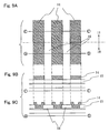
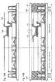
- FIGS. 2A and 2B are cross-sectional views taken along a line b-b' in FIG. 3. In the case of conventional structures as shown in FIGS. 2A and 2B, an
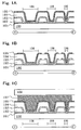
end face 2 of aninterlayer insulating film 1 is always exposed to outer atmosphere. Therefore, there is a case that water enters through the interlayer insulating film and deterioration of a light emitting element is caused, even when an upper portion thereof is covered with animpermeable sealant 3 so that alight emitting element 4 is not exposed to outer air. - Thus, one of structures in the present invention for solving the problem is described with reference to FIGS. 1A to 1C. FIGS. 1A to 1C show an example of reducing water entry through the interlayer insulating film by covering inside of a groove formed on the periphery of the interlayer insulating film with an impermeable film (hereinafter, referred to as a protective film). FIGS. 1A to 1C correspond to a cross section taken along a line d-d' in FIG. 3, for example. Note that a sealant made of an impermeable material and an opposing substrate are omitted in FIGS. 1A and 1B. A state of the periphery of an electroluminescent device is shown.
Reference numeral 100 denotes a substrate; 101, a base insulating film; 102, a first interlayer insulating film; 103, a first protective film; 104, a second interlayer insulating film; and 105, a second protective film. - In this structure, the first
interlayer insulating film 102 and the secondinterlayer insulating film 104 are assumed comparatively highly permeable. In these highly permeable films, a groove-shapedopening 106 that penetrates each film in a thickness direction is formed. Theprotective films protective films opening 106. - When such a structure is employed, water entered from edge portions of the interlayer insulating
films protective films opening 106. Since the groove-shapedopening 106 is formed to penetrate in a thickness direction, an entry path of water is blocked without providing the protective film. Therefore, providing the groove-shaped opening alone becomes a countermeasure for deterioration of a light emitting element due to water, depending on desired degree of reliability. - The groove-shaped
opening 106 is the most effective when continuously formed all around the periphery of the permeable film. However, when it is impossible, a certain degree of effect can be expected by forming the opening only on one side or partially since water entry at least from the portion can be reduced. - In FIGS. 1A to 1C, the groove-shaped
opening 106 is repeatedly provided from the periphery of the interlayer insulating film to a region provided with a light emitting element, but only one groove-shapedopening 106 may as well be provided. However, reliability is further improved by repeatedly taking such measures. - When the
protective films protective films - Other structures of suppressing water entry by such a groove-shaped opening and a protective film are conceivable, and some examples of them are given in FIGS. 4A and 4B. Cross-sectional views shown in FIGS. 4A and 4B also correspond to a line d-d' in FIG. 3 or the like. In addition, a sealant made of an impermeable material and an opposing substrate are omitted.
- FIGS. 1A to 1C show an example that positions of a first opening formed in the first
interlayer insulating film 102 and a second opening formed in the secondinterlayer insulating film 104 are the same; however, FIGS. 4A and 4B show an example that positions of the first opening formed in the firstinterlayer insulating film 102 and the second opening formed in the secondinterlayer insulating film 104 are different. Even such a structure can achieve an effect similar to the structure as shown in FIGS. 1A to 1C and can be formed in a short time since the second opening is shallower than that in FIGS. 1A to 1C. In addition, less attention to disconnection between steps needs to be paid since level difference becomes small. In FIG. 4A and FIG. 4B, a position in which an opening is formed is difference. - In addition, the
substrate 100 provided with the light emitting element is fixed to an opposingsubstrate 108 with asealant 107 made of an impermeable material, and the light emitting element is sealed from the outside. The sealant is more effective in suppressing water entry when formed in an upper portion of the groove-shapedopening 106. - In this embodiment mode, the case of two layers of the interlayer insulating films is described; however, the present invention can be applied in the case of one layer.
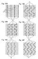
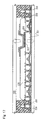
- In this embodiment mode, an example of a structure for preventing water from entering by removing a permeable film on the periphery of a substrate from the periphery of the substrate to a certain distance is described with reference to FIGS. 5A and 5B. Here, the permeable film is assumed an interlayer insulating film. However, an object is not limited to the interlayer insulating film and the present invention can be applied as a countermeasure for the permeable film. The cross-sectional views correspond to a line e-e' in FIG. 3.
-
Reference numeral 120 denotes a portion from which theinterlayer insulating films Embodiment Mode 1, the end faces of the interlayer insulatingfilms films protective films - When the
sealant 107 made of an impermeable material is formed on an outer side of the end face of the interlayer insulating film covered with the protective film or is formed to cover the entire end face of the interlayer insulating film in fixing the opposingsubstrate 108, water entry can further be prevented. Therefore, improvement in reliability can be expected. - In addition, other structures in this embodiment mode are conceivable, and one example of them is shown in FIG. 5B. A difference between FIG. 5B and FIG. 5A is a removed position of the interlayer insulating
films interlayer insulating film 104 is located on the further outer side of the substrate than the end face of the firstinterlayer insulating film 102, and FIG. 5B shows a structure in which the end face of the firstinterlayer insulating film 102 is located on the further outer side of the substrate than the end face of the secondinterlayer insulating film 104. - Note that two layers of the interlayer insulating films are used in this embodiment mode; however, the present invention can be applied to an electroluminescent device having one layer of an interlayer insulating film.
- Moreover, this embodiment mode is more effective when combined with
Embodiment Mode 1. - As is obvious referring to FIGS. 6A to 6C, in the case of manufacturing a sealing structure of the present invention, an
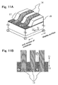
opening 106 and an interlayer insulating film removedportion 120 on an end face of a substrate can be formed simultaneously with opening of a contact hole formed in interlayer insulatingfilms - However, a contact hole is etched under such a condition that the interlayer insulating film and a gate insulating film can be etched using a silicon semiconductor layer as an etching stopper. In the
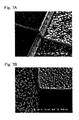
opening 106 and the interlayer insulating film removedportion 120 where an etching stopper does not exist, an etching residue may be generated, or abase insulating film 101 may be sharpened, thereby generating unevenness, in etching the firstinterlayer insulating film 102. - FIG. 7A is a SEM picture of a sample in which a siloxane film is formed over a base film as an interlayer insulating film, a silicon nitride film is formed thereover, a part of the interlayer insulating film is removed under an opening condition of a contact hole, and then a wiring is provided. Regions indicated by "C" and "c" are regions from which the interlayer insulating film is removed, and regions "a", "b", and "c" are provided with a wiring. A region "A" is an original surface without being etched, "B" is an end face of the interlayer insulating film, and "C" is a surface of the base insulating film.
- As is obvious seeing this, small unevenness as shown in the region "C" is generated when a contact hole is formed in the interlayer insulating film under the contact hole opening condition to reach the base insulating film. Then, large unevenness as shown in the region "c" is generated by forming a wiring thereover. It is obvious from evenness of a wiring formed over the region "a" that this unevenness is caused by unevenness over the base insulating film after forming the opening. The wiring can be used as a protective film, and this may cause to generate unevenness over the protective film. In addition, coverage of the wiring itself becomes poor.
- When such large unevenness is generated, adhesiveness of a sealant made of an impermeable material to be formed thereover may be in danger of being significantly affected. This is because water enters from a portion having poor adhesiveness when the sealant has poor adhesiveness, even when the sealant itself has low permeability.
- As in FIG. 7A, FIG. 7B is a SEM picture of a sample in which a siloxane film is formed over a base insulating film as an interlayer insulating film, the interlayer insulating film is removed under the contact hole opening condition, and then a wiring is provided. The region "C" in FIG. 7A corresponds to a region "D" in FIG. 7B, and the region "D" is a surface from which the interlayer insulating film is removed under the contact hole opening condition after forming a base insulating film and an interlayer insulating film in this order over the substrate. The region "c" in FIG. 7A corresponds to a region "E" in FIG. 7B, and the region "E" is a surface in which a wiring is formed over the region "D" in FIG. 7B.
- On the other hand, a region "F" in FIG. 7B is a surface of a portion from which the interlayer insulating film is removed under the contact hole opening condition similarly as in the region "D" in FIG. 7B after forming the base insulating film, a silicon film, and the interlayer insulating film in this order over the substrate, that is, forming the silicon film serving as an etching stopper over the base insulating film and forming the interlayer insulating film thereover. Briefly, it has a structure of the region "D" in FIG. 7B provided with an etching stopper of the silicon film. Since the silicon film in the region "F" is removed by etching in forming the wiring in "E", the base insulating film can be seen similarly as in the region "D" in FIG. 7B. The region "F" has a very even surface in comparison with "D" in which a silicon film is not formed under the interlayer insulating film.
- This is because the silicon film serves as an etching stopper film and suppresses generation of an etching residue of the interlayer insulating film in etching the interlayer insulating film and generation of unevenness due to gouge of the base insulating film.
- On the basis of this, in this embodiment mode,
etching stopper films opening 106 in FIGS. 1A to 1C and the interlayer insulating film removedportion 120 in FIGS. 5A and 5B (FIG. 6A). Cross-sectional views shown in FIGS. 6A to 6C correspond to a cross-section taken along a line f-f in FIG. 3. - An example of forming such
etching stopper films semiconductor layer 132 of a thin film transistor (TFT) manufactured in a driver circuit portion or a pixel portion is described in this embodiment mode. However, any film can be used as theetching stopper films opening 106 and the interlayer insulating film removedportion 120 in removing the interlayer insulating film. It may be made of the same material as thesemiconductor layer 132 simultaneously with formation of thesemiconductor layer 132 as in this embodiment mode; it may be made of the same material as thegate electrode 133 simultaneously with formation of the gate electrode; or it may separately be made of another material. When it is formed simultaneously with thesemiconductor layer 132 or the gate insulating film, it is advantageous since the number of processes does not increase. - The
opening 106 and the interlayer insulating film removedportion 120 are formed simultaneously with a contact hole opening for the wiring. In this case, theetching stopper films 130 and 131 (silicon film) are formed in a lower portion of theopening 106 and the interlayer insulating film removedportion 120 in a light emitting device of the present invention. Therefore, unevenness due to an etching residue or gouge of the interlayer insulating film is not generated. If awiring 134 to be formed later is formed to cover inside of theopening 106 and the end face of the interlayer insulating film in the interlayer insulating film removedportion 120, it also functions as aprotective film 103. When the interlayer insulating film is removed using theetching stopper films protective film 103 can be prevented from decreasing, and generation of unevenness on the protective film can be suppressed. - In this embodiment mode, the
protective film 103 is made of the same metal film as a material for thewiring 134, and can be formed simultaneously with the step of forming the wiring. However, it may be made of another material in a different step. - In addition, the
protective film 103 may further be covered with a material for ananode 135 of the light emitting element over a switching TFT of a pixel portion to be formed later. It can be expected that water entry can further be suppressed (FIG. 6B). - An opposing
substrate 108 is fixed with asealant 107 made of an impermeable material after forming the light emitting element. The sealant can block an entry path of water by being applied over the groove-shapedopening 106 and/or the interlayer insulating film removedportion 120 on the periphery of the substrate. Therefore, the sealant is highly effective in suppressing deterioration of the light emitting element. The light emitting element is formed by interposing alight emitting layer 137 between theanode 135 and acathode 138, and the light emitting element is separated from every element by a partition 136 (FIG. 6C). - When this embodiment mode is applied, generation of unevenness of the
protective film 103 over the groove-shapedopening 106 and the interlayer insulating film removedportion 120 on the periphery of the substrate are suppressed. Therefore, deterioration of adhesiveness of the sealant can be prevented, and water entry from a portion having poor adhesiveness can be suppressed, which improves reliability. - This embodiment mode can freely be combined with
Embodiment Mode - In this embodiment mode, a structure is described, which can suppress an effect of water entered through an interlayer insulating film in a structure in which it is difficult to remove an entire interlayer insulating film.
- As described in
Embodiment Modes sealant 107. However, there may be a case that it is difficult to remove an entire interlayer insulating film, depending on a structure. - For example, a wiring portion connecting an external terminal and an internal circuit is considered (a region "c" in FIG. 3). The wiring is formed by removing an interlayer insulating film on the periphery of a substrate, forming a metal film serving as a wiring, and etching the metal film to have a desired shape of a wiring, when a structure in which an interlayer insulating film on the periphery of a substrate is removed (a structure in which an interlayer insulating film removed
portion 120 is formed:Embodiment Modes 2 and 3) is employed. - However, there is a
step 12 that an end face of an interlayer insulating film forms between aportion 10 from which aninterlayer insulating film 15 is removed and aportion 11 in which the interlayer insulating film remains. There is a case that a metal film formed in this portion is not sufficiently etched and remains. Such anetching residue 13 makesadjacent wirings 14 short circuit and causes a defect. - A measure that an
interlayer insulating film 16 is left between the wirings 14 is taken as shown in FIG. 9 to lessen the interlayer insulating film which is exposed to outer air while preventing the short circuit. Accordingly, a defect due to the above described short circuit can be prevented with most of the interlayer insulating film prevented from being exposed to outer air. However, the interlayer insulating film left between the wirings cannot be removed and is always exposed to outer air; therefore, water entry from the portion cannot be prevented. Water entry from the interlayer insulating film remaining between the wirings may have an adverse effect when considered from the point of view of long-term reliability. - Water entry through the interlayer insulating film is caused by a diffusion phenomenon of water in the film. As for the diffusion phenomenon, it is assumed that time to reach a certain position is proportional to square of distance as is found by a formula of diffusion. Namely, when only the interlayer insulating film left between the wirings is an entry path of water, time for water which enters by diffusing in the interlayer insulating film left between electrodes to reach inside of an electroluminescent device can effectively be lengthened by taking the distance as long as possible.
- Conventionally, the wiring portion which connects an external terminal and an internal circuit is straight as shown in FIG. 10A besides a place where a bend is necessary in terms of layout, such as a corner. The
wiring 14 is thickly provided with a plurality of bends as shown in FIG. 10B. - Then, substantial length of the
interlayer insulating film 16 existing between the wirings can be lengtheed, and a distance for water to diffuse in the interlayer insulating film before reaching inside of the electroluminescent device becomes longer. Consequently, time to start to deteriorate can largely be obtained, and longer-term reliability can be secured than ever before. - FIGS. 10C to 10F show examples of other conceivable structures for realizing this embodiment mode. When length of the interlayer insulating film between wirings gets longer even a little than the conventional structure in FIG. 10A, water entry can further be delayed than ever before. A desired pattern may be formed depending on necessity.
- When this embodiment mode is applied, area of the interlayer insulating film between the wirings when looked from above of a light emitting device becomes large. Therefore, it is important to dispose a bend of the wiring in such a position that it is not exposed to outer air, that is, inside a sealant made of an impermeable material or in a lower portion of the sealant.
- This embodiment mode can be applied by appropriately combining with
Embodiment Modes 1 to 3. It is possible to effectively prevent water entry by separately applying Embodiment Modes according to its location, for example, applying this embodiment mode to a wiring portion connecting an external terminal and an internal circuit of an electroluminescent device (a region "c" in FIG. 3 or the like), andEmbodiment Modes Embodiment Mode 3 is employed on that occasion, generation of unevenness over the wiring can be suppressed. Therefore, adhesiveness of a sealant made of an impermeable material is improved, and water entry from an interface between the sealant and the wiring can drastically be decreased. - In this embodiment mode, a mode which can remove an interlayer insulating film on the periphery of a substrate also in a wiring portion (a region "c" in FIG. 3 or the like) connecting an external terminal and an internal circuit and prevent water entry through an interlayer insulating film is described with reference to FIGS. 11A and 11B.
- It is only in a
step 12 on an end face of aninterlayer insulating film 15 where an etching residue is generated since it cannot be etched, as shown in FIG. 8. Since the end face of the interlayer insulating film is steep, a wiring material may not be etched by anisotropic dry etching employed for wiring formation and may remain in this portion. In such a wiring portion, it is difficult to employ isotropic etching typified by wet etching in terms of a margin of the wiring. - Thus, the
end face 17 of theinterlayer insulating film 18 is processed into a gently tapered shape in this embodiment mode. Accordingly, a wiring can certainly be etched even on theend face 17 of the interlayer insulating film, and an etching residue can be prevented from generating; therefore, it becomes unnecessary to leave the interlayer insulating film between the wirings 14 (FIGS. 11A and 11B). - As a result, the interlayer insulating film on the periphery of a substrate can entirely be removed in the wiring portion (a region "c" in FIG. 3 or the like) connecting an external terminal and an internal circuit. Moreover, a water path through the interlayer insulating film can completely be blocked by covering whole outer periphery than a position where the interlayer insulating film exists with an impermeable sealant. Then, reliability of an electroluminescent device can drastically be improved.
- Note that the tapered end face of the interlayer insulating film may be processed with an inert gas such as argon. This densifies an end face of the wiring, and has an effect of making it harder for an impurity such as water to enter, compared to the case without processing. In addition, it is preferable to further form a nitride film such as a silicon nitride film to cover the tapered end face of the interlayer insulating film, since water entry from the end face can similarly be suppressed.
- This embodiment mode can be applied by appropriately combining with
Embodiment Modes Embodiment modes - An example of combining Embodiment Mode 5 and
Embodiment Mode 3 is described in this embodiment mode. - In this embodiment mode combining Embodiment Mode 5 and
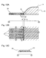
Embodiment Mode 3, anetching stopper film 20 is formed in aportion 10 from which an interlayer insulating film is removed in order to suppress generation of unevenness caused in etching an interlayer insulating film. In this case, a film serving as an etching stopper is formed in a lower portion of a remaininginterlayer insulating film 15 in terms of amargin 21 for forming an end face of an interlayer insulating film into a tapered shape (FIG. 12A). - The
etching stopper film 20 is formed over an entire surface of the interlayer insulating film removedportion 10, and awiring 14 is formed thereover. Therefore, when theetching stopper film 20 has conductivity, all the wirings formed in the interlayer insulating film removed portion are short-circuited. However, the etching stopper film in aposition 22 where a wiring is not formed is etched and removed with an unnecessary metal film in etching for forming a wiring shape, or is removed by performing appropriate etching again in the case where it cannot be removed by wiring etching. Therefore, there is no need to worry about a short circuit between wirings in the portion. However, anetching stopper film 23 located in a lower portion of the above described remaining interlayer insulating film (theetching stopper film 20 in a position of a taper formation margin 21) remains without being removed since it is covered with the interlayer insulating film. When the film has conductivity, a problem that wirings are short-circuited through the portion is caused (ref. FIG. 12B). - Such a problem does not occur when the etching stopper film is made of an insulating film. However, in the case of forming the etching stopper film without increasing the number of steps, the problem notably occurs since a conceivable film is a silicon film used for a semiconductor layer or a metal film used for a gate electrode and both of them have conductivity.
- In this embodiment mode, among the etching stopper film formed below the interlayer insulating film, an etching stopper film is not formed between wirings from the beginning (FIGS. 13A to 13D). Among the etching stopper film formed below the interlayer insulating film, an etching stopper film is formed to be separated from the etching stopper film located in a lower portion of the wiring (FIGS. 18F to 18I).
- When this structure is employed, generation of unevenness in removing an interlayer insulating film can be suppressed also in a wiring portion connecting an external terminal and an internal circuit and unevenness of a wiring can also be suppressed. Accordingly, decrease in adhesiveness of a sealant due to unevenness of a lower film can be prevented, and water entry from a portion having poor adhesiveness of a sealant can drastically be reduced. Consequently, reliability of an electroluminescent device is exceedingly improved.
- In this embodiment, a detailed embodiment of
Embodiment Mode 1 andEmbodiment Mode 2 is described with reference to FIGS. 14A and 14B, 15A and 15B, and 16A and 16B. - A first
interlayer insulating film 225 is formed over asubstrate 200 provided with abase insulating film 201, a driver circuit transistor (only an n-channelthin film transistor 203 and a p-channelthin film transistor 204 are shown in the drawing), and a thin film transistor in a pixel portion (only a switchingtransistor 205 and acurrent control transistor 206 are shown in the drawing). - An insulating substrate such as a glass substrate, a quartz substrate, or a crystalline glass, a ceramic substrate, a stainless steel substrate, a metal substrate (tantalum, tungsten, molybdenum, or the like), a semiconductor substrate, a plastic substrate (polyimide, acrylic, polyethylene terephthalate, polycarbonate, polyarylate, polyethersulfone, or the like), or the like can be used as the
substrate 200, but a material which can withstand at least heat generated during a process. In this embodiment, a glass substrate is employed. - A silicon oxide film, a silicon nitride film, a silicon oxynitride film, or the like can be used as the
base insulating film 201. These are formed by using a known method such as sputtering, low pressure CVD, plasma CVD, or the like. In this embodiment, a silicon nitride oxide film is formed to be 100 nm in thickness. - Subsequently, an amorphous semiconductor film is formed. The amorphous semiconductor film may be made of silicon or a material containing silicon as its main component (for example, SixGe1-x, or the like) to have a desired thickness. As a manufacturing method, a known method such as sputtering, low pressure CVD, plasma CVD can be employed. In this embodiment, the amorphous semiconductor film is made of amorphous silicon to be 50 nm in thickness.
- Next, amorphous silicon is crystallized. A step of performing laser crystallization after adding an element that promotes crystallization and crystallizing by heat treatment is described in this embodiment.
- A thin film of a nickel solution is formed on the surface of the semiconductor film by applying with a spinner a nickel acetate solution or a nickel nitrate solution containing nickel in a concentration of from 5 ppm to 10 ppm in terms of weight. The nickel element may be sprayed on the whole surface of the semiconductor film by sputtering instead of application. As a catalytic element, one of or a plurality of elements such as iron (Fe), palladium (Pd), tin (Sn), lead (Pb), cobalt (Co), platinum (Pt), copper (Cu), and gold (Au) may be used as well as nickel (Ni).
- Subsequently, the amorphous semiconductor film is crystallized by heat treatment. It may be carried out at a temperature of from 500 °C to 650 °C for about 4 hours to 24 hours since a catalytic element is used. The semiconductor film becomes a crystalline semiconductor film according to this crystallization process.
- Subsequently, crystallization by a laser is performed to improve crystallinity. For laser crystallization, a pulse oscillation or continuous oscillation gas, solid, or metal laser oscillation device may be used. A laser oscillated from a laser oscillation device may be radiated in a linear shape by using an optical system.
- The semiconductor film crystallized by using metal that promotes the crystallization as in this embodiment contains a metal element used for crystallization in the film. As this residue may cause various disadvantages, the concentration thereof is required to be lowered by gettering.
- First, the surface of the crystallized semiconductor film is treated with ozone water, and then a barrier film is formed to have a thickness of from 1 nm to 5 nm, over which a gettering site is formed by sputtering. The gettering site is formed by depositing an amorphous silicon film containing an argon element of 50 nm in thickness. Thereafter, gettering is carried out by heating at 750 °C for 3 minutes by using a lamp annealing device to remove the gettering site.
- After gettering, the crystalline semiconductor film is etched into
semiconductor layers 207 to 210 having desired shapes. Thereafter, agate insulating film 211 is formed. An insulating film containing silicon may be formed in a thickness of approximately 115 nm by low pressure CVD, plasma CVD, sputtering, or the like. A silicon oxide film is formed in this embodiment. - A tantalum nitride (TaN) film of 30 nm in thickness is formed as a first conductive layer over the
gate insulating film 211, and a tungsten (W) film of 370 nm in thickness is formed as a second conductive layer thereover. Note that the first conductive layer is a TaN film of 30 nm in thickness and the second conductive layer is a W film of 370 nm in thickness in this embodiment; however, the present invention is not limited thereto. The first and second conductive layers may be made of any element selected from Ta, W, Ti, Mo, Al, Cu, Cr, and Nd, or an alloy or compound material having the above element as a main component. Furthermore, a semiconductor film typified by a polycrystalline silicon film doped with an impurity element such as phosphorous may be used. The first conductive layer may be formed to have a thickness of from 20 nm to 100 nm, and the second conductive layer may be formed to have a thickness of from 100 nm to 400 nm. In this embodiment, a laminated structure of two layers is employed; however, a single layer structure may be employed, or three or more layers may be laminated as well. - In order to form an electrode and a wiring by etching the conductive layer, a resist is formed as a mask through exposure to light by photolithography. First etching treatment is carried out under first and second etching conditions. Etching is carried out using the mask made of a resist to form a gate electrode and a wiring. An etching condition may be determined in each case.
- In this method, ICP (Inductively Coupled Plasma) etching is used. As the first etching condition, CF4, Cl2, and O2 are used as an etching gas with the gas-flow ratio of 25/25/10 (sccm), and a pressure of 1.0 Pa and an RF (13.56 MHz) power of 500 W is applied on a coil electrode to generate plasma for etching. An RF (13.56 MHz) power of 150 W is applied to a substrate side (sample stage) to apply a substantially negative self bias voltage. The W film is etched under the first etching condition to make an edge portion of the first conductive layer into a tapered shape. An etching rate on the W film under the first etching condition is 200.39 nm/min, the etching rate on the TaN film is 80.32 nm/min, and the selectivity ratio of W relative to TaN is approximately 2.5. Further, a taper angle of the W film is about 26° under the first etching condition.
- Subsequently, etching is carried out under the second etching condition. Etching is performed for about 15 seconds with the resist as a mask remained, by using CF4 and Cl2 as an etching gas with the gas-flow ratio of 30/30 (sccm), and a pressure of 1.0 Pa and an RF (13.56 MHz) power of 500 W is applied on the coil electrode to generate plasma for etching. An RF (13.56 MHz) power of 20 W is applied to a substrate side (sample stage) to apply a substantially negative self bias voltage. Under the second etching condition in which CF4 and Cl2 are mixed, both of the W film and the TaN film are etched to the same extent. The edge portions of the first and second conductive layers become tapered in the first etching due to bias voltage applied to the substrate.
- The second etching is carried out without removing the resist as a mask. The second etching is performed using SF6, Cl2, and O2 as an etching gas with the gas-flow ratio of 24/12/24 (sccm), and a pressure of 1.3 Pa and an RF (13.56 MHz) power of 700 W is applied on the coil electrode to generate plasma for etching for about 25 seconds. An RF (13.56 MHz) power of 10 W is applied to a substrate side (sample stage) to apply a substantially negative self bias voltage. The W film is selectively etched under this etching condition to form a conductive layer in a second shape. The first conductive layer is hardly etched at this time. Gate electrodes including the first
conductive layers 212a to 215a and the secondconductive layers 212b to 215b are formed by the first and second etching. - First doping is carried out without removing the resist as a mask. Thus, an N-type impurity is doped in a low concentration into a crystalline semiconductor layer. The first doping may be performed by ion doping or ion implantation. The ion doping may be performed with the dose amount of from 1 x 10¹³ atoms/cm2 to 5 x 10¹⁴ atoms/cm2, and an acceleration voltage of from 40 kV to 80 kV. The ion doping is carried out at an acceleration voltage of 50 kV in this embodiment. The N-type impurity may be an element belonging to the
group 15 of the periodic table typified by phosphorous (P) or arsenic (As). Phosphorous (P) is used in this embodiment. The first conductive layer is used as a mask to form a first impurity region (N-- region) in a self-aligned manner to which an impurity of low concentration is doped. - Subsequently, the resist as a mask is removed. Then, a mask made of a resist is newly formed and the second doping is carried out at a higher acceleration voltage than the first doping. The N-type impurity is doped in the second doping as well. The ion doping may be performed with the dose amount of from 1 x 10¹³ atoms/cm2 to 3 x 10¹⁵ atoms/cm2, and an acceleration voltage of from 60 kV to 120 kV. The ion doping is carried out with the dose amount of 3.0 x 10¹⁵ atoms/cm2 and an acceleration voltage of 65 kV in this embodiment. The second doping is carried out so that the impurity element is doped into the semiconductor layer under the first conductive layer by using the second conductive layer as a mask against the impurity element.
- By the second doping, a second impurity region (N- region, Lov region) is formed on the part where the second conductive layer is not overlapped or the part which is not covered with the mask in the part where the crystalline semiconductor layer is overlapped with the first conductive layer. The N-type impurity of which concentration ranging from 1 x 10¹⁸ atoms/cm3 to 5 x 10¹⁹ atoms/cm3 is doped into the second impurity region. Further, the exposed part (third impurity region: N+ region) which is not covered with either the conductive layer in a first shape nor the mask is doped with a high concentration N-type impurity ranging from 1 x 10¹⁹ atoms/cm3 to 5 x 10²¹ atoms/cm3. The semiconductor layer has an N+ region, a part of which is covered only with the mask. The concentration of the N-type impurity of this part is not changed from the impurity concentration of the first doping. Therefore, this part is referred to as the first impurity region (N-- region) as it is.
- Note that each impurity region is formed by two doping treatment in this embodiment; however, the invention is not exclusively limited to this. The impurity region having a desired impurity concentration may be formed by one or multiple doping by determining the condition in each case.
- Subsequently, the resist as a mask is removed and a mask made of a resist is newly formed for third doping. By the third doping, a fourth impurity region (P+ region) and a fifth impurity region (P- region) are formed in which an impurity element having the opposite conductivity to the ones of the first and second conductive layers is added to a semiconductor layer serving as a P channel TFT.
- The fourth impurity region (P+ region) is formed on the part which is not covered with the resist as a mask and not overlapped with the first conductive layer, and the fifth impurity region (P- region) is formed on the part which is not covered with the resist as a mask, overlapped with the first conductive layer, and not overlapped with the second conductive layer. The P-type impurity element may be boron (B), aluminum (Al), or gallium (Ga), each of which belongs to the
group 13 of the periodic table. - In this embodiment, boron is used as a P-type impurity element to form the fourth and fifth impurity regions by ion doping using diborane (B2H6). Ion doping is carried out with the dose amount of 1 x 10¹⁶ atoms/cm2 and an acceleration voltage of 80 kV.
- Note that semiconductor layers 207 and 209 for forming N-channel TFTs are covered with the mask made of a resist in the third doping.
- The fourth impurity region (P+ region) and the fifth impurity region (P- region) are doped with phosphorous of different concentrations by the first and second doping. However, in both of the fourth impurity region (P+ region) and the fifth impurity region (P' region), the third doping is performed so that the concentration of the P-type impurity element is from 1 x 10¹⁹ atoms/cm2 to 5 x 10²¹ atoms/cm2. Therefore, the fourth impurity region (P+ region) and the fifth impurity region (P- region) work as a source region and a drain region of a P-channel TFT without problems.
- It should be noted that the fourth impurity region (P+ region) and the fifth impurity region (P- region) are formed by once third doping; however, the invention is not exclusively limited to this. The fourth impurity region (P+ region) and the fifth impurity region (P- region) may be formed by multiple doping treatments according to each condition.
- By the aforementioned doping treatment, a first impurity region (N-- region) 216, a second impurity region (N- region, Lov region) 217, third impurity regions (N+ region) 218 and 219, fourth impurity regions (P+ region) 220 and 221, and fifth impurity regions (P- region) 222 and 223 are formed.
- Thereafter, a
first passivation film 224 is formed over a gate electrode and a gate insulating film. A silicon nitride film, a silicon oxynitride film, or a silicon nitride oxide film containing hydrogen is formed as the first passivation film. - Subsequently, the first
interlayer insulating film 225 is formed. After a siloxane polymer is entirely applied as the first interlayer insulating film, it is dried by heat treatment at a temperature of from 50 °C to 200 °C for 10 minutes, and baking treatment is performed at a temperature of from 300 °C to 450 °C for 1 hour to 12 hours. A siloxane film having a thickness of 1 µm, in which a skeletal structure is made up of a bond of silicon (Si) and oxygen (O), is formed over an entire surface by the baking. This step can hydrogenate a semiconductor layer by hydrogen contained in thefirst passivation film 224 as well as baking the siloxane polymer; consequently, the number of steps can be reduced and processes can be simplified. - An inorganic insulating film, an organic material resin, a low-k material, or the like formed by a known method such as a CVD method can be used for the first interlayer insulating film.
- Thereafter, a silicon nitride oxide film or a silicon oxynitride film may be formed by a CVD method to cover the first
interlayer insulating film 225. When a conductive film to be formed later is etched, this film functions as an etching stopper and can prevent the interlayer insulating film from being overetched. Further, a silicon nitride film may be formed thereover by sputtering. The silicon nitride film has a function of suppressing movement of an alkaline metal ion; therefore, a metal ion from a pixel electrode to be formed later, such as a lithium element or sodium can be prevented from moving to a semiconductor thin film. - Subsequently, the first interlayer insulating film is patterned and etched to form a
contact hole 226 reaching thethin film transistors 203 to 206, a groove-shapedopening 227, and an interlayer insulating film removedportion 228 on the periphery of a substrate. - The
contact hole 226, theopening 227, and the interlayer insulating film removedportion 228 can be formed by etching the siloxane film using a mixed gas of CF4, O2, and He, and then etching and removing the silicon oxide film that is a gate insulating film using a CHF3 gas. - Subsequently, a metal film is laminated within the
contact hole 226 and is patterned to form a source electrode and a drain electrode. In this embodiment, a titanium film including a nitrogen atom, a titanium-aluminum alloy film, and a titanium film are laminated to be 100 nm/350 nm/100 nm in thickness, respectively. Then, the films are patterned and etched into a desired shape to form source/drain electrodes 229 to 235 and apixel electrode 236 of three layers. - A titanium film including a nitrogen atom in the first layer is formed by sputtering using titanium as a target with a flow rate of nitrogen and argon set 1:1. When the titanium film including a nitrogen atom as described above is formed over an interlayer insulating film made of a siloxane film, a wiring which is hardly peeled and which has a low resistance connection with a semiconductor region can be formed.
- In this embodiment, a top gate polysilicon TFT is formed in both a driver circuit portion and a pixel portion; however, a TFT in the pixel portion may be a TFT using amorphous silicon as an active layer or a TFT using microcrystalline silicon as an active layer. In addition, a bottom gate TFT can naturally be used.
- At the same time that a source electrode and a drain electrode are formed, a first
protective film 237 is made of the same material to cover inside of the groove-shapedopening 227 and an end face of the interlayer insulating film removedportion 228 on the periphery of the substrate. - Subsequently, a second
interlayer insulating film 238 is formed over an entire surface of the substrate. The secondinterlayer insulating film 238 can be made of the same material as the firstinterlayer insulating film 225. In this embodiment, the secondinterlayer insulating film 238 is made of the same siloxane film as the first interlayer insulating film. - Thereafter, a
contact hole 239, a groove-shapedopening 240, and an interlayer insulating film removedportion 241 on the periphery of the substrate, which are to be connected to a pixel electrode, are formed under the same condition as that in etching the first interlayer insulating film. - In this embodiment, both the first
interlayer insulating film 225 and the secondinterlayer insulating film 238 are made of a siloxane film; however, a structure of the interlayer insulating film is not limited thereto. The structure can appropriately be changed to a combination of an organic film for the first interlayer insulating film and an inorganic film for the second interlayer insulating film, the opposite combination thereof, a combination of an organic film and an organic film, a combination of an inorganic film and an inorganic film, or the like. A protective film may be formed only over either the first interlayer insulating film or the second interlayer insulating film depending on permeability of a selected interlayer film. - After a contact hole is formed in the second
interlayer insulating film 238, a first electrode serving as an anode of a light emitting element is continuously formed in thecontact hole 239 connected to the pixel electrode and over the secondinterlayer insulating film 238. An electrode of the light emitting element is a laminate of Al-Si(260a)/TiN(260b)/ITSO(260c). Here, Al-Si is aluminum containing silicon of approximately from 1 atomic% to 5 atomic%, and ITSO is a material in which ITO is mixed with SiO2. - At the same time that the anode of the light emitting element is formed, inside of the groove-shaped
opening 240 and the end face of theinterlayer insulating film 238 at the interlayer insulating film removedportion 241 on the periphery of the substrate is covered with aprotective film 242. The protective film may be formed with theelectrodes 260a to 260c of the light emitting element. All of the threelayers 260a to 260c may be used, or one or two of the layers may be used. - Subsequently, an
insulator 243 is formed to cover an end face of the first electrode. Theinsulator 243 can be made of an inorganic or organic material. Silicon oxide, silicon oxynitride, siloxane, acrylic, polyimide, or the like can be given. It is preferable to form theinsulator 243 by using a photosensitive organic material, since a shape of the opening becomes such a shape that a radius of curvature continuously changes and disconnection between the steps or the like hardly occurs when evaporating a light emitting layer. - Then, evaporation is performed with an evaporation source moving by using an evaporation apparatus. For example, evaporation is performed in a film formation chamber which is vacuum evacuated to 5 x 10⁻³ Torr (0.665 Pa) or less, preferably to from 10-4 Torr to 10-6 Torr. When evaporation is performed, an organic compound is previously vaporized by resistance heating and flies in a direction of the substrate when a shutter is opened in evaporation. The vaporized organic compound flies upwardly and is evaporated to the substrate through an opening provided for a metal mask to form a light emitting layer 244 (including a hole transport layer, a hole injection layer, an electron transport layer, and an electron injection layer).
- In this embodiment, the light emitting layer is formed by evaporation; therefore, a low molecular weight light-emitting material is used. However, the light emitting layer is formed also by using a high molecular weight material and an intermediate molecular weight material having characteristics between a low molecular weight material and a high molecular weight material. A high molecular weight material can be applied using spin coating or ink jetting by dissolving into a solvent. In addition, a composite material with an inorganic material as well as an organic material can also be used.
- It is assumed that a light emitting mechanism of a light emitting element emits light in such a way that an electron injected from a cathode and a hole injected from an anode form a molecular exciton by recombining at the center of light emission in an organic compound layer when voltage is applied to the organic compound layer interposed between a pair of electrodes, and energy for light emission is released when the molecular exciton turns back to the ground state. The excited state is known to include a singlet excited state and a triplet excited state, through either of which light can be emitted.
- A light emitting layer typically has a laminated structure. The typical laminated structure is constituted as "a hole transport layer, an electroluminescent layer, and an electron transport layer." This structure has such a high luminous efficiency that light emitting devices that are recently researched and developed mostly employ this structure. A structure in which a hole injection layer, a hole transport layer, an electroluminescent layer, and an electron transport layer are laminated over the anode in this order, or a structure in which a hole injection layer, a hole transport layer, an electroluminescent layer, an electron transport layer, and an electron injection layer are laminated over the anode in this order may be employed as well. A fluorescent pigment or the like may be doped into the electroluminescent layer.
- Subsequently, a
second electrode 245 is formed as a cathode over the light emitting layer. Thesecond electrode 245 may be made of a thin film containing a metal with a low work function (Li, Mg, or Cs). In addition, it is preferable that the second electrode is made of a laminated film in which a transparent conductive film (ITO (indium tin oxide), indium zinc oxide (In2O3-ZnO), zinc oxide (ZnO), or the like) is laminated over the thin film containing Li, Mg, Cs, or the like. Further, the second electrode may be formed to be from 0.01 µm to 1 µm in thickness by electron beam evaporation, although the film thickness may be determined appropriately to serve as a cathode. - Such a light emitting element enables both monochrome display and multicolor display by selection and arrangement of the light emitting layer. For monochrome display, all light emitting elements are manufactured by using one material; however, there are several methods for multicolor display. One is a separately coloring method. The separately coloring method realize multicolor display by separately coloring a light emitting layer which emits light of an objective color in a necessary portion. Another method is a color conversion method. Light emitting layers are made of one material, and a color conversion layer is provided only in a necessary portion. Light emitted from the light emitting layer is converted into a desired color through the color conversion layer, thereby realizing multicolor display. Another method is a method for providing a color filter for a white light emitting element. This method realizes multicolor display by forming a light emitting layer which emits white light all over the pixel portion and by passing through a color filter. In all of the methods, the light emitting layer is formed so that three primary colors of light of RGB are provided every pixel in the case of full color display. Thus, the light emitting device can perform monochrome, multicolor, and full color display.
- An opposing
substrate 248 is fixed to the substrate with asealant 247 made of an impermeable material for sealing after alight emitting element 246 is completed in this way. Thesealant 247 made of an impermeable material further firmly blocks off a water entrance and entry path when formed to cover an end face of an interlayer insulating film covered with a protective film in the groove-shapedopenings portions sealant 247 made of an impermeable material. - According to the above described steps, an electroluminescent device resistant to deterioration due to water entered from exterior can be manufactured, and reliability of the electroluminescent device can drastically be improved. Note that only one groove-shaped opening around an interlayer insulating film in a sealing portion is provided in this embodiment; however, a plurality of openings can be provided. Reliability is further improved by providing a plurality of openings.
- In this embodiment, an embodiment regarding Embodiment Mode 5 and Embodiment Mode 6 is described with reference to FIGS. 17 and 18A to 18I. In FIG. 17, an interlayer insulating film has a single layer structure; however, it may be regarded as having the same structure as in
Embodiment 1. A structure of a first electrode in a light emitting element is different, but it is described below. - FIG. 17 is a cross-sectional view taken along a line f-f in FIG. 3. In FIG. 17, an
etching stopper film 250 is formed in a groove-shaped opening on the periphery of an interlayer insulating film and in an interlayer insulating film removed portion on the periphery of a substrate. Theetching stopper film 250 can be formed at the same time as formation of a semiconductor layer of a transistor in a driver circuit portion or a pixel portion. It functions as an etching stopper in etching aninterlayer insulating film 251 and has effect of improving adhesiveness of a sealant made of an impermeable material by reducing generation of an etching residue or unevenness. - Since it is similar to
Embodiment 1 up to manufacturing a source electrode and a drain electrode except to have theetching stopper film 250, explanation is omitted. After a source electrode and a drain electrode are formed, afirst electrode 252 of a light emitting element is formed to be in contact with anelectrode 255 of a switching TFT in a pixel portion. In this embodiment, thefirst electrode 252 of the light emitting element is manufactured over an interlayer insulating film provided with the source electrode and the drain electrode. Therefore, it is not necessary to manufacture a second interlayer insulating film. A material similar to the first electrode inEmbodiment 1 can be used as a material for thefirst electrode 252 or the like, and a process after manufacturing the first electrode is similar toEmbodiment 1; therefore, explanation is omitted. - Here, light can be extracted in a direction of a
substrate 200 when the first electrode is made of a transparent conductive film typified by ITO. In addition, light can be extracted in both directions of thesubstrate 200 and an opposingsubstrate 248 when a second electrode is also similarly made of a transparent material. - FIGS. 18A to 18I show a method for manufacturing a region "c" in FIG. 3. FIGS. 18A to 18E are cross-sectional views taken along a line a-a' in FIG. 3, and FIGS. 18F to 18I are top views of the region "c" in FIG. 3. FIGS. 18A to 18E and FIGS. 18F to18I adjacent to each other respectively show a diagram of the same step. In FIGS. 18A to 18I, a left side is a direction of an FPC and a right side is a direction of a display portion. Since FIGS. 18F to 18l have a direction different from that in the region "c" in FIG. 3, it is necessary to be paid attention to.
- When a transistor and a first insulating film are formed in a display portion in this embodiment, a base insulating film 301 is formed over a
substrate 300 in a wiring portion connecting an external terminal and an internal circuit. An etching stopper film 302 (silicon film) is formed in a portion from which an interlayer film is removed over the base insulating film 301; an insulatingfilm 303 functioning as a gate insulating film is formed to cover the etching stopper film 302 (silicon film) and the base insulating film 301; and then, a firstinterlayer insulating film 304 is formed to cover the same. An acrylic film or a siloxane film can be employed for the first interlayer film; however, a siloxane film is used in this embodiment (FIGS. 18A and 18F). - Thereafter, the first
interlayer insulating film 304 is etched and removed to have a tapered shape on an end face thereof, thereby forming an interlayer insulating film removedportion 305 on the periphery of the substrate. The etching stopper film 302 (silicon film) serving as an etching stopper is formed in advance in the interlayer insulating film removedportion 305. Therefore, a surface of the interlayer insulating film removedportion 305 after removal is even, and unevenness due to an etching residue or gouge of a base film is not caused. (FIGS. 18B and 18G) - Subsequently, a
metal film 306 serving as a wiring is formed. The metal film may be made of the same material as the source electrode and the drain electrode in the driver circuit portion or the pixel portion. A specific material is similar to the material for the source electrode and the drain electrode in Embodiment 1 (FIGS. 18C and 18H). - The
metal film 306 is etched simultaneously with etching for forming the source electrode and the drain electrode in order to form awiring 307. At this time, a portion without being covered with thewiring 307 of the etching stopper film 302 (silicon film) formed in the interlayer insulating film removedportion 305 is removed by the etching. When anetching stopper film 302 which is not located below thewiring 307 and is formed in aposition 308 below a remaininginterlayer insulating film 304 is previously formed in such a shape that it is separated from the etching stopper film 309 (silicon film) located below thewiring 307 after wiring etching, wirings adjacent to each other do not short-circuit, even if theetching stopper film 302 is made of a conductive material (FIGS. 18D, 18E, and 18I). - Generation of unevenness in the interlayer insulating film removed
portion 305 can be prevented and generation of large unevenness on a wiring to be formed thereafter can also be suppressed by forming the etching stopper film 302 (silicon film) as an etching stopper. Adhesiveness of a sealant made of an impermeable material to be formed thereover can be maintained, and water entering from a portion having poor adhesiveness of a sealant can be reduced. - When such a structure is employed, an interlayer insulating film can be removed also in a wiring portion connecting an external terminal portion (such as an FPC) and an internal circuit, and the interlayer insulating film can be prevented from being exposed to outer air. Consequently, water entry can drastically be reduced, which contributes to improvement in reliability of an electroluminescent device.
- After removing the first interlayer insulating film on the periphery of the substrate to have a tapered shape on its end face and before forming metal for a wiring, it is useful to form a nitride film such as a silicon nitride film or a carbon nitride film thereover by CVD in order to prevent moisture from entering from an end face (not shown). Higher reliability can be obtained by forming such a nitride film.
- In this embodiment, the first interlayer insulating film on the periphery of the substrate is removed by the same step as opening of a contact hole in a pixel portion and a driver circuit portion. Therefore, in the pixel portion and a driver circuit portion, conduction between a wiring in a lower layer or the like and a wiring formed over the first interlayer insulating film, which is to be performed through the contact hole, may not be made, when the nitride film is formed after removing the first interlayer insulating film. Thus, in a portion which is required to electrically be in contact with a lower portion, a nitride film in the portion is preferably removed before forming metal for a wiring. When a nitride film is formed over the first interlayer insulating film, moisture can be prevented from entering from an end face of an interlayer insulating film in such a contact hole portion. Consequently, further higher reliability can be obtained.
- In this embodiment, an example of a pixel structure in an electroluminescent device to which a structure of the present invention is applied is described with reference to FIGS. 19A and 19B.
- FIGS. 19A and 19B show an element structure of one pixel. The display portion in FIG. 3 is formed by arranging a plurality of such pixels in matrix. Naturally, this pixel structure is merely an example, and any other conceivable pixel structures may be employed.
- In FIGS. 19A and 19B, a top emission structure is adopted. One pixel includes a
source line 400, a driverTFT gate line 401, ananode line 402, an erasinggate line 403, awriting gate line 404, an erasingTFT 405, a writingTFT 406, adriver TFT 407, adisplay TFT 408, anAC driving diode 409, acapacitor 410, adrain electrode 411 of a driver TFT, and a driverTFT gate line 412. - Then, a
light emitting element 413 is formed in an upper portion thereof through an insulating film, and an anode or a cathode of a light emitting element is connected to thedrain electrode 411 of a driver TFT. - In this embodiment, a structure of a source driver that is required to display an image in an electroluminescent device is described with reference to FIG. 20.
- In a row where a gate signal line is selected, a shift register 500 (SR) outputs a sampling pulse sequentially from a first stage in accordance with a
clock pulse 504 and astart pulse 505. Afirst latch circuit 501 takes in a video signal in timing with a sampling pulse being inputted, and the video signal taken in at each stage is stored in thefirst latch circuit 501. - According to a sampling pulse outputted from one
shift register 500, three latch circuits A, B, and C in thefirst latch circuit 501 take in signals inputted from video lines DATA 01 to 20,DATA 21 to 40, DATA 41 to 60, respectively. A sampling pulse outputted from theshift register 500 in the first stage takes in a video signal for being charged and discharged in a source signal line from S01 to S60 among source signal lines from S01 to S1920. In the first latch circuit that takes in a video signal in response to a sampling pulse of theshift register 500 in the first stage, the latch circuit A stores a video signal for source signal lines from S01 to S20; B, from S21 to S40; and C, from S41 to S60. Subsequently, the first latch circuit that takes in a video signal in response to a sampling pulse outputted from the shift register in the second stage takes in a video signal for source signal lines from S61 to S120. The latch circuits A, B, and C store a video signal for source signal lines from S61 to S80, from S81 to S100, and from S101 to S120, respectively. Similarly, a shift register in the 32nd stage takes in and stores a video signal for source signal lines from S1861 to S1920; then, taking in a video signal for one row is completed. - When a latch pulse (LAT) 506 is outputted after taking in a video signal for one row is completed, the video signal stored in the
first latch circuit 501 is transferred to asecond latch circuit 502 all at once, and all signal lines are charged and discharged all at once. A level shifter and a buffer for making output from the second latch circuit 502 a desired size may appropriately be provided as necessary. - The above-mentioned operation is repeated from the first row to the last row, thereby completing writing for one frame. Thereafter, similar operations are repeated to display an image.
- Note that a source driver having this structure is merely an example, and the present invention can be applied even if any other structures of a source driver are employed.
- A method for forming an end face of an insulating film into a tapered shape as described in Embodiment Mode 5 is described in this embodiment.
- When isotropic etching such as wet etching can be performed and there are a margin in etching and a certain film thickness, a tapered shape can easily be obtained.
- A method for forming an insulating film into a tapered shape by anisotropic dry etching is described in this embodiment.
- First, a method for processing an object into a desired shape by dry etching using an etching mask previously manufactured by a conventional method is described with reference to FIGS. 21A to 21E.
- A
mask material 602 such as a photosensitive resist or polyimide is formed over an entire surface of an object to be processed 601 by application or the like (FIG. 21A). A positive resist is given as an example in this description. - Subsequently, pre-bake at low temperature for vaporizing and stabilizing a material in the resist is performed; thereafter, the resist is partially exposed to light through a
photomask 603 in a desired shape (FIG. 21B). - After a portion exposed to light by the light-exposure is dissolved in developer and is removed (FIG. 21C), baking is performed to improve adhesiveness of the resist and to improve resistance to an etchant to be used in the next step. An etching mask for an object is formed so far. The step so far is referred to as photolithography.
- An object can be processed into a desired shape by etching the object using the mask and an appropriate etchant (FIG. 21D).
- Here, the end face of the etching mask is at large angle to the object located in a lower portion. Therefore, the end face of the object which is located in a lower portion becomes steep reflecting the shape of the end face of the etching mask, when anisotropic etching such as dry etching is performed. When an interlayer insulating film on the periphery of the substrate is removed and a wiring is formed in such a way, an etching residue of a wiring as described in
Embodiment Mode 4 or 5 is generated on an end face of the interlayer insulating film, which causes a defect due to wiring short circuit. - Consequently, in forming a mask by photolithography, a
slit 605 having narrower width than limit of resolution of a photolithography apparatus used for light-exposure is formed on an end face of a portion of thephotomask 604 which is preferably formed into a tapered shape. A mask material such as a resist which is exposed to light through a slit and a pattern having narrower width than resolution of a photolithography apparatus is not completely exposed to light in the portion. A mask of which film thickness is decreased remains even after removing a light-exposed portion with developer. - An incomplete light-exposed portion as described above is provided between a non-light-exposed portion and a complete light-exposed portion in a photosensitive mask material such as a resist by thus forming a slit or a hole having width equal to or narrower than light-exposure resolution of a photolithography apparatus in a photomask. Accordingly, an end face of an etching mask can be formed into a tapered shape.
- When anisotropic etching typified by dry etching is performed using the etching mask having a tapered shape under such a condition that both the object in a lower layer and the mask are etched, the etching mask disappears where thickness thereof is thin at the same time that the object is etched. According to disappearance of the etching mask, an object newly exposed to etching atmosphere is sequentially etched, thereby obtaining an object having a shape nearly reflecting a shape of the etching mask (FIGS. 21F to 21J).
- An object (an interlayer insulating film in Embodiment Mode 5) having a similar tapered shape on an end face thereof is obtained by using the etching mask having a tapered shape on an end face thereof.
- A shape of a photosensitive material after development can freely be formed depending on shapes of a slit, a pattern, and a hole of a photomask in exposing to light. FIGS. 22A to 22D show an example thereof. FIGS. 22A and 22C are SEM pictures of a sample in which a siloxane film is formed over a substrate, a resist is applied thereover, exposed to light with a
photomask 700, and etched by dry etching, and FIGS. 22B and 22D are schematic diagrams of a photomask. The SEM pictures show that a resist is exposed to light with a photomask having such a pattern as thephotomask 700 shown in FIG. 22B or 22D. - While only a
portion 701 is exposed to light with a typical photomask, a cross-sectional shape as shown in the SEM picture can be obtained in FIGS.22A to 22D by forming apattern 702 equal to or narrower than limit of resolution of a photolithography apparatus in a photomask. - As shown in FIGS. 22A to 22D, an object can have various shapes by changing a shape of the
pattern 702 equal to or narrower than limit of resolution of a photolithography apparatus. An object having a shape that cannot be formed ever before can be manufactured by appropriately changing an object material and an etching condition using the thus formed etching mask. - Examples of electronic devices to which the present invention is applied can be given as a video camera, a digital camera, a goggle type display (head mounted display), a navigation system, an audio reproducing device (car audio, an audio component, or the like), a laptop personal computer, a game machine, a personal digital assistant (a mobile computer, a cellular phone, a portable game machine, an electronic book, or the like), and an image reproducing device including a recording medium (specifically, a device capable of processing data in a recording medium such as a Digital Versatile Disk (DVD) and having a display that can display the image of the data). Practical examples of these electronic devices are shown in FIGS. 23A to 23E.
- FIG. 23A shows a wall-mounted display device, which includes a
chassis 2001, adisplay portion 2003, aspeaker portion 2004, and the like. The present invention is applied to manufacturing of thedisplay portion 2003. Longer-term reliability can be secured by employing the present invention. - FIG. 23B shows a digital still camera, which includes a
main body 2101, adisplay portion 2102, animage receiving portion 2103,operation keys 2104, anexternal connection port 2105, ashutter 2106, and the like. The present invention can be applied to thedisplay portion 2102. Although a digital still camera is often used outside and tends to be put in a harder condition than indoors, long-term reliability can be obtained even under a comparatively hard condition by employing the present invention. - FIG. 23C shows a laptop personal computer, which includes a
main body 2201, achassis 2202, adisplay portion 2203, akeyboard 2204, anexternal connection port 2205, apointing mouse 2206, and the like. The present invention can be applied to thedisplay portion 2203. A laptop personal computer can conceivably be carried around and used, which is different from a desktop computer. Similarly as a digital still camera, possibility of use under a more adverse condition than a monitor of a desktop computer increases by being carried around. Longer-term reliability can be secured even under such a condition by employing the present invention. - FIG. 23D shows a mobile computer, which includes a
main body 2301, adisplay portion 2302, aswitch 2303,operation keys 2304, aninfrared port 2305, and the like. The present invention can be applied to thedisplay portion 2302. Although a mobile computer is often used outside and tends to be put in a harder condition than indoors, long-term reliability can be obtained even under a comparatively hard condition by employing the present invention. - FIG. 23E shows a portable game machine, which includes a
chassis 2401, adisplay portion 2402, aspeaker portion 2403,operation keys 2404, a recordingmedium insertion portion 2405, and the like. The present invention can be applied to thedisplay portion 2402. Although a portable game machine is often used outside and tends to be put in a harder condition than indoors, long-term reliability can be obtained even under a comparatively hard condition by employing the present invention. - As described above, the applicable range of the present invention is so wide that the invention can be applied to electronic devices of various fields. In addition, reliability of a product improves, so that reliability as a manufacturer can also be improved.
- This application is based on Japanese Patent Application serial no. 2003-347601 filed in Japan Patent Office on Aug. 29 in 2003 and no. 2003-322334 filed on Sept. 12 in 2003, the contents of which are hereby incorporated by reference.
- Although the present invention has been fully described by way of example with reference to the accompanying drawings, it is to be understood that various changes and modifications will be apparent to those skilled in the art. Therefore, unless otherwise such changes and modifications depart from the scope of the present invention hereinafter defined, they should be construed as being included therein.
Claims (137)
- A light emitting device comprising:wherein at least one of the first and second substrate is transparent.a first substrate;a first interlayer insulating film formed over the first substrate;a second interlayer insulating film formed over the first interlayer insulating film;a light emitting element formed on the second interlayer insulating film;a second substrate provided over the light emitting element,a first opening which penetrates the first interlayer insulating film, formed at a peripheral portion of the first interlayer insulating film;a first protective film covering the first opening and the first interlayer insulating film; anda second opening which penetrates the second interlayer insulating film, formed at a peripheral portion of the second interlayer insulating film,
- A light emitting device according to Claim 1, wherein the first protective film is impermeable.
- A light emitting device according to Claim 1, wherein the light emitting element is electrically connected to a thin film transistor.
- A light emitting device according to Claim 1, wherein the first protective film comprises the same material as a source electrode and a drain electrode of the thin film transistor.
- A light emitting device according to Claim 1, wherein a semiconductor film is formed in a bottom portion of the first opening.
- A light emitting device according to Claim 1, wherein a metal film is formed in a bottom portion of the first opening.
- A light emitting device according to Claim 1, wherein a semiconductor film is formed in a bottom portion of the first opening, and the semiconductor film comprises the same material as an active layer of the thin film transistor.
- A light emitting device according to Claim 1, wherein a metal film is formed in a bottom portion of the first opening, and the metal film comprises the same material as a gate electrode of the thin film transistor.
- A light emitting device according to Claim 1, wherein at least a portion of a bottom of the first opening and a portion of the bottom of the second opening are formed in the same position over the substrate.
- A light emitting device according to Claim 1, wherein a bottom of the first opening and the bottom of the second opening are formed in a different position over the substrate.
- A light emitting device according to Claim 1, wherein the first opening is formed in the first interlayer insulating film and the second opening is formed in the second interlayer insulating film.
- A light emitting device according to Claim 1, wherein at least one of the first interlayer insulating film and the second interlayer insulating film comprises an organic material.
- A light emitting device according to Claims 1, wherein at least one of the first interlayer insulating film and the second interlayer insulating film comprises an inorganic material.
- A light emitting device according to Claim 1, wherein at least one of the first interlayer insulating film and the second interlayer insulating film comprises a film including siloxane moiety.
- A light emitting device according to Claim 12, wherein the organic material is acrylic.
- A light emitting device according to Claim 12, wherein the organic material is polyimide.
- A light emitting device according to Claim 1, wherein the first protective film is a silicon nitride film.
- A light emitting device according to Claim 1, wherein the light emitting device is incorporated into an electronic device selected from the group consisting of a display device, a camera, a computer, a portable information terminal, and a game apparatus.
- A light emitting device comprising:wherein at least one of the first and second substrate is transparent.a first substrate;a first interlayer insulating film formed over the first substrate;a second interlayer insulating film formed over the first interlayer insulating film;a light emitting element formed over the second interlayer insulating film;a second substrate provided over the light emitting element,a first opening which penetrates the first interlayer insulating film, formed at a peripheral portion of the first interlayer insulating film;a first protective film covering the first opening and the first interlayer insulating film;a second opening which penetrates the second interlayer insulating film, formed at a peripheral portion of the second interlayer insulating film; anda second protective film covering the second opening and the second interlayer insulating film and contacting with the first impermeable protective film at a bottom surface of the second opening;
- A light emitting device according to Claim 19, where in the first protective film is impermeable.
- A light emitting device according to Claim 19, where in the second protective film is impermeable.
- A light emitting device according to Claim 19, wherein the second protective film comprises the same material as an anode or a cathode of the light emitting element.
- A light emitting device according to Claim 19, wherein the light emitting element is electrically connected to a thin film transistor.
- A light emitting device according to Claim 19, wherein the first protective film comprises the same material as a source electrode and a drain electrode of the thin film transistor.
- A light emitting device according to Claim 19, wherein a semiconductor film is formed in a bottom portion of the first opening.
- A light emitting device according to Claim 19, wherein a metal film is formed in a bottom portion of the first opening.
- A light emitting device according to Claim 19, wherein a semiconductor film is formed in a bottom portion of the first opening, and the semiconductor film comprises the same material as an active layer of the thin film transistor.
- A light emitting device according to Claim 19, wherein a metal film is formed in a bottom portion of the first opening, and the metal film comprises the same material as a gate electrode of the thin film transistor.
- A light emitting device according to Claim 19, wherein at least a portion of a bottom of the first opening and a portion of the bottom of the second opening are formed in the same position over the substrate.
- A light emitting device according to Claim 19, wherein a bottom of the first opening and the bottom of the second opening are formed in a different position over the substrate.
- A light emitting device according to Claim 19, wherein the first opening is formed in the first interlayer insulating film and the second opening is formed in the second interlayer insulating film.
- A light emitting device according to Claim 19, wherein at least one of the first interlayer insulating film and the second interlayer insulating film comprises an organic material.
- A light emitting device according to Claim 19, wherein at least one of the first interlayer insulating film and the second interlayer insulating film comprises an inorganic material.
- A light emitting device according to Claim 19, wherein at least one of the first interlayer insulating film and the second interlayer insulating film comprises a film including siloxane moiety.
- A light emitting device according to Claim 32, wherein the organic material is acrylic or polyimide.
- A light emitting device according to Claim 19, wherein the first protective film or the second protective film is a silicon nitride film.
- A light emitting device according to Claim 19, wherein the first protective film and the second protective film are silicon nitride films.
- A light emitting device according to Claim 19, wherein the light emitting device is incorporated into an electronic device selected from the group consisting of a display device, a camera, a computer, a portable information terminal, and a game apparatus.
- A light emitting device comprising:wherein the first and second substrates are fixed to each other at a first region provided with the first and second openings or in a second region outside of the first region, anda first substrate;a first interlayer insulating film formed over the first substrate;a second interlayer insulating film formed over the first interlayer insulating film;a light emitting element formed over the second interlayer insulating film;a second substrate provided over the light emitting element;a first opening which penetrates the first interlayer insulating film, formed at a peripheral portion of the first interlayer insulating film;a first protective film covering the first opening and the first interlayer insulating film;a second opening which penetrates the second interlayer insulating film, formed at a peripheral portion of the second interlayer insulating film; anda second protective film covering the second opening and the second interlayer insulating film and contacting with the first impermeable protective film at a bottom surface of the second opening,
wherein at least one of the first and second substrate is transparent. - A light emitting device according to Claim 39, where in the first protective film is impermeable.
- A light emitting device according to Claim 39, where in the second protective film is impermeable.
- A light emitting device according to Claim 39, wherein the second protective film comprises the same material as an anode or a cathode of the light emitting element.
- A light emitting device according to Claim 39, wherein the light emitting element is electrically connected to a thin film transistor.
- A light emitting device according to Claim 39, wherein the first protective film comprises the same material as a source electrode and a drain electrode of the thin film transistor.
- A light emitting device according to Claim 39, wherein a semiconductor film is formed in a bottom portion of the first opening.
- A light emitting device according to Claim 39, wherein a metal film is formed in a bottom portion of the first opening.
- A light emitting device according to Claim 39, wherein a semiconductor film is formed in a bottom portion of the first opening, and the semiconductor film comprises the same material as an active layer of the thin film transistor.
- A light emitting device according to Claim 39, wherein a metal film is formed in a bottom portion of the first opening, and the metal film comprises the same material as a gate electrode of the thin film transistor.
- A light emitting device according to Claim 39, wherein at least a portion of a bottom of the first opening and a portion of the bottom of the second opening are formed in the same position on a face of the substrate.
- A light emitting device according to Claim 39, wherein a bottom of the first opening and the bottom of the second opening are formed in a different position on a face of the substrate.
- A light emitting device according to Claim 39, wherein the first opening is formed in the first interlayer insulating film and the second opening is formed in the second interlayer insulating film.
- A light emitting device according to Claim 39, wherein at least one of the first interlayer insulating film and the second interlayer insulating film comprises an organic material.
- A light emitting device according to Claim 39, wherein at least one of the first interlayer insulating film and the second interlayer insulating film comprises an inorganic material.
- A light emitting device according to Claim 39, wherein at least one of the first interlayer insulating film and the second interlayer insulating film comprises a film including siloxane moiety.
- A light emitting device according to Claim 52, wherein the organic material is acrylic.
- A light emitting device according to Claim 52, wherein the organic material is polyimide.
- A light emitting device according to Claim 39, wherein the first protective film or the second protective film is a silicon nitride film.
- A light emitting device according to Claim 39, wherein the first protective film and the second protective film are silicon nitride films.
- A light emitting device according to Claim 39, wherein the light emitting device is incorporated into an electronic device selected from the group consisting of a display device, a camera, a computer, a portable information terminal, and a game apparatus.
- A light emitting device comprising:wherein a side surface of the interlayer insulating film is tapered at a region not to reach an edge portion of the first substrate, anda first substrate;an interlayer insulating film formed over the first substrate;a light emitting element formed over the interlayer insulating film; anda second substrate provided over the light emitting element,
wherein at least one of the first and second substrate is transparent. - A light emitting device according to Claim 60, wherein the light emitting element is electrically connected to a thin film transistor.
- A light emitting device according to Claim 60, wherein a semiconductor film is formed from a bottom portion of the interlayer insulating film to the edge portion of the substrate.
- A light emitting device according to Claim 60, wherein a metal film is formed from a bottom portion of the interlayer insulating film to the edge portion of the substrate.
- A light emitting device according to Claim 60, wherein a semiconductor film is formed from a bottom portion of the interlayer insulating film to the edge portion of the substrate, and the semiconductor film comprises the same material as an active layer of the thin film transistor.
- A light emitting device according to Claim 60, wherein a metal film is formed from a bottom portion of the interlayer insulating film to the edge portion of the substrate, and the metal film comprises the same material as a gate electrode of the thin film transistor.
- A light emitting device according to Claim 60, wherein the interlayer insulating film comprises an organic material.
- A light emitting device according to Claim 60, wherein the interlayer insulating film comprises an inorganic material.
- A light emitting device according to Claims 60, wherein the interlayer insulating film comprises a film including siloxane moiety.
- A light emitting device according to Claim 66, wherein the organic material is acrylic.
- A light emitting device according to Claim 66, wherein the organic material is polyimide.
- A light emitting device according to Claim 60, wherein the protective film is a silicon nitride film.
- A light emitting device according to Claim 60, wherein the light emitting device is incorporated into an electronic device selected from the group consisting of a display device, a camera, a computer, a portable information terminal, and a game apparatus.
- A light emitting device comprising:wherein a side surface of the interlayer insulating film is tapered at a region not to reach an edge portion of the first substrate, anda first substrate;an interlayer insulating film formed over the first substrate;a light emitting element formed over the interlayer insulating film;a second substrate provided over the light emitting element, andan protective film formed on a-side surface of the interlayer insulating film,
wherein at least one of the first and second substrate is transparent. - A light emitting device according to Claim 73, wherein the light emitting element is electrically connected to a thin film transistor.
- A light emitting device according to Claim 73, wherein a semiconductor film is formed from a bottom portion of the interlayer insulating film to the edge portion of the substrate.
- A light emitting device according to Claim 73, wherein a metal film is formed from a bottom portion of the interlayer insulating film to the edge portion of the substrate.
- A light emitting device according to Claim 73, wherein a semiconductor film is formed from a bottom portion of the interlayer insulating film to the edge portion of the substrate, and the semiconductor film comprises the same material as an active layer of the thin film transistor.
- A light emitting device according to Claim 73, wherein a metal film is formed from a lower portion of the interlayer insulating film to the edge portion of the substrate, and the metal film comprises the same material as a gate electrode of the thin film transistor.
- A light emitting device according to Claim 73, wherein the interlayer insulating film comprises an organic material.
- A light emitting device according to Claim 73, wherein the interlayer insulating film comprises an inorganic material.
- A light emitting device according to Claims 73, wherein the interlayer insulating film comprises a film including siloxane moiety.
- A light emitting device according to Claim 79, wherein the organic material is acrylic.
- A light emitting device according to Claim 79, wherein the organic material is polyimide.
- A light emitting device according to Claim 73, wherein the protective film is a silicon nitride film.
- A light emitting device according to Claim 73, wherein the protective film is impermeable.
- A light emitting device according to Claim 73, wherein the light emitting device is incorporated into an electronic device selected from the group consisting of a display device, a camera, a computer, a portable information terminal, and a game apparatus.
- A light emitting device comprising:wherein a side surface of the interlayer insulating film is tapered at a region not to reach an edge portion of the first substrate,a first substrate;an interlayer insulating film formed over the first substrate;a light emitting element formed over the interlayer insulating film;a second substrate provided over the light emitting element, andan protective film formed on a side surface of the interlayer insulating film,
wherein at least one of the first and second substrate is transparent, and
wherein the first and second substrates are fixed to each other at a first region in which the side surface of the interlayer insulating film is provided, or at a second region outside of the first region. - A light emitting device according to Claim 87, wherein the light emitting element is electrically connected to a thin film transistor.
- A light emitting device according to Claim 87, wherein a semiconductor film is formed from a bottom portion of the interlayer insulating film to the edge portion of the substrate.
- A light emitting device according to Claim 87, wherein a metal film is formed from a bottom portion of the interlayer insulating film to the edge portion of the substrate.
- A light emitting device according to Claim 81, wherein a semiconductor film is formed from a bottom portion of the interlayer insulating film to the edge portion of the substrate, and the semiconductor film comprises the same material as an active layer of the thin film transistor.
- A light emitting device according to Claim 87, wherein a metal film is formed from a lower portion of the interlayer insulating film to the edge portion of the substrate, and the metal film comprises the same material as a gate electrode of the thin film transistor.
- A light emitting device according to Claim 87, wherein the interlayer insulating film comprises an organic material.
- A light emitting device according to Claim 87, wherein the interlayer insulating film comprises an inorganic material.
- A light emitting device according to Claims 87, wherein the interlayer insulating film comprises a film including siloxane moiety.
- A light emitting device according to Claim 93, wherein the organic material is acrylic.
- A light emitting device according to Claim93, wherein the organic material is polyimide.
- A light emitting device according to Claim 87, wherein the protective film is a silicon nitride film.
- A light emitting device according to Claim 87, wherein the protective film is impermeable.
- A light emitting device according to Claim 87, wherein the light emitting device is incorporated into an electronic device selected from the group consisting of a display device, a camera, a computer, a portable information terminal, and a game apparatus.
- A light emitting device comprising:wherein the first wiring is adjacent to the second wiring with interlayer insulating film interposed therebetween,a first substrate;a pixel portion over the first substrate;the pixel portion comprising a light emitting element over an interlayer insulating film;an external connection portion inputting a signal to the pixel portion;at least a first wiring and a second wiring connecting to the pixel portion and the external connection portion; anda sealing member fixing the first substrate and a second substrate between the pixel portion and the external connection portion,
wherein at least one of the first wiring and the second wiring include at least one bend portion, and
wherein the first wiring and the second wiring are covered with the sealing material. - A light emitting device according to Claim 101, wherein the light emitting element is electrically connected to a thin film transistor.
- A light emitting device according to Claim 101, wherein the first protective film comprises the same material as a source electrode and a drain electrode of the thin film transistor.
- A light emitting device according to Claim 101, wherein at least one layer of the first interlayer insulating film and the second interlayer insulating film comprises an organic material.
- A light emitting device according to Claims 101, wherein at least one layer of the first interlayer insulating film and the second interlayer insulating film comprises an inorganic material.
- A light emitting device according to Claim 101, wherein at least one layer of the first interlayer insulating film and the second interlayer insulating film comprises a film including siloxane moiety.
- A light emitting device according to Claim 101 , wherein the organic material is acrylic.
- A light emitting device according to Claim 104, wherein the organic material is polyimide.
- A light emitting device according to Claim 104, wherein the first protective film is a silicon nitride film.
- A light emitting device according to Claim 101, wherein the light emitting element is electrically connected to a thin film transistor.
- A light emitting device according to Claim 101, wherein the light emitting device is incorporated into an electronic device selected from the group consisting of a display device, a camera, a computer, a portable information terminal, and a game apparatus.
- A light emitting device comprising:wherein a side surface of the interlayer insulating film is tapered at a region in which the first and second substrates are fixed to each other with a sealing material.a first substrate;an interlayer insulating film formed over the first substrate;a light emitting element formed over the interlayer insulating film;a second substrate provided over the light emitting element,
- A light emitting device according to Claim 112, wherein the light emitting element is electrically connected to a thin film transistor.
- A light emitting device according to Claim 112, wherein the interlayer insulating film comprises an organic material.
- A light emitting device according to Claims 112, the interlayer insulating film comprises an inorganic material.
- A light emitting device according to Claim 112, wherein the interlayer insulating film comprises a film including siloxane moiety.
- A light emitting device according to Claim 114 , wherein the organic material is acrylic.
- A light emitting device according to Claim 114, wherein the organic material is polyimide.
- A light emitting device according to Claim 112, wherein the light emitting device is incorporated into an electronic device selected from the group consisting of a display device, a camera, a computer, a portable information terminal, and a game apparatus.
- A light emitting device comprising:wherein a first opening is formed in the first interlayer insulating film at a region in which the first and second substrates are fixed to each other with a sealing material,a first substrate;a first interlayer insulating film formed over the first substrate;a second interlayer insulating film formed over the first interlayer insulating film;a light emitting element formed over the interlayer insulating film;a second substrate provided over the light emitting element,
wherein the first opening is covered with a first protective film,
wherein a second opening is formed in the second interlayer insulating film at the region, and
wherein the second opening is covered with a second protective film. - A light emitting device according to the Claim 120, the protective film is impermeable.
- A light emitting device according to Claim 120, wherein the light emitting element is electrically connected to a thin film transistor.
- A light emitting device according to Claim 120, wherein the interlayer insulating film comprises an organic material.
- A light emitting device according to Claims 120, the interlayer insulating film comprises an inorganic material.
- A light emitting device according to Claim 120, wherein the interlayer insulating film comprises a film including siloxane moiety.
- A light emitting device according to Claim 123, wherein the organic material is acrylic.
- A light emitting device according to Claim 123, wherein the organic material is polyimide.
- A light emitting device according to Claim 120, wherein the light emitting device is incorporated into an electronic device selected from the group consisting of a display device, a camera, a computer, a portable information terminal, and a game apparatus.
- A light emitting device comprising:wherein a first opening is formed in the first interlayer insulating film at a region in which the first and second substrates are fixed to each other with a sealing material,a first substrate;a first interlayer insulating film formed over the first substrate;a light emitting element formed over the first interlayer insulating film;a second interlayer insulating film formed over the first interlayer insulating film; anda second substrate provided over the light emitting element,
wherein the first opening is covered with a first protective film,
wherein a second opening is formed in the second interlayer insulating film at the region,
wherein the second opening is covered with a second protective film, and
wherein a side surface of the interlayer insulating film is tapered at a region in which the first and second substrates are fixed to each other with a sealing material. - A light emitting device according to the Claim 129, the protective film is impermeable.
- A light emitting device according to Claim 129, wherein the light emitting element is electrically connected to a thin film transistor.
- A light emitting device according to Claim 129, wherein the interlayer insulating film comprises an organic material.
- A light emitting device according to Claims 129, the interlayer insulating film comprises an inorganic material.
- A light emitting device according to Claim 129, wherein the interlayer insulating film comprises a film including siloxane moiety.
- A light emitting device according to Claim 132 , wherein the organic material is acrylic.
- A light emitting device according to Claim 132, wherein the organic material is polyimide.
- A light emitting device according to Claim 129, wherein the light emitting device is incorporated into an electronic device selected from the group consisting of a display device, a camera, a computer, a portable information terminal, and a game apparatus.
Applications Claiming Priority (4)
| Application Number | Priority Date | Filing Date | Title |
|---|---|---|---|
| JP2003347601 | 2003-08-29 | ||
| JP2003347601 | 2003-08-29 | ||
| JP2003322334 | 2003-09-12 | ||
| JP2003322334 | 2003-09-12 |
Publications (3)
| Publication Number | Publication Date |
|---|---|
| EP1511081A2 true EP1511081A2 (en) | 2005-03-02 |
| EP1511081A3 EP1511081A3 (en) | 2010-03-03 |
| EP1511081B1 EP1511081B1 (en) | 2019-10-09 |
Family
ID=34106978
Family Applications (1)
| Application Number | Title | Priority Date | Filing Date |
|---|---|---|---|
| EP04019744.4A Expired - Fee Related EP1511081B1 (en) | 2003-08-29 | 2004-08-19 | Light emitting device |
Country Status (5)
| Country | Link |
|---|---|
| US (5) | US7928654B2 (en) |
| EP (1) | EP1511081B1 (en) |
| KR (2) | KR101158830B1 (en) |
| CN (2) | CN100459184C (en) |
| TW (6) | TWI571168B (en) |
Cited By (6)
| Publication number | Priority date | Publication date | Assignee | Title |
|---|---|---|---|---|
| EP1601031A1 (en) * | 2004-05-28 | 2005-11-30 | Samsung SDI Co., Ltd. | Organic light emitting device and method of fabricating the same |
| EP2105964A1 (en) | 2008-02-28 | 2009-09-30 | Samsung Mobile Display Co., Ltd. | Organic light emitting display device |
| EP1814183A3 (en) * | 2006-01-26 | 2011-05-25 | Samsung Mobile Display Co., Ltd. | Organic light-emitting display device |
| EP2267780A3 (en) * | 2009-06-26 | 2014-03-26 | Mitsubishi Electric Corporation | Image display element and manufacturing method thereof |
| EP2267779A3 (en) * | 2009-06-26 | 2014-03-26 | Mitsubishi Electric Corporation | Image display element and manufacturing method thereof |
| US11372276B2 (en) | 2014-11-26 | 2022-06-28 | Semiconductor Energy Laboratory Co., Ltd. | Display device and electronic device |
Families Citing this family (58)
| Publication number | Priority date | Publication date | Assignee | Title |
|---|---|---|---|---|
| SG142140A1 (en) | 2003-06-27 | 2008-05-28 | Semiconductor Energy Lab | Display device and method of manufacturing thereof |
| US7928654B2 (en) | 2003-08-29 | 2011-04-19 | Semiconductor Energy Laboratory Co., Ltd. | Display device and method for manufacturing the same |
| JP4741177B2 (en) * | 2003-08-29 | 2011-08-03 | 株式会社半導体エネルギー研究所 | Method for manufacturing display device |
| KR100561646B1 (en) * | 2003-10-23 | 2006-03-20 | 엘지.필립스 엘시디 주식회사 | Thin Film Transistor Substrate for Display Device And Method For Fabricating The Same |
| US7619258B2 (en) * | 2004-03-16 | 2009-11-17 | Semiconductor Energy Laboratory Co., Ltd. | Display device |
| US7183147B2 (en) * | 2004-03-25 | 2007-02-27 | Semiconductor Energy Laboratory Co., Ltd. | Light emitting device, method for manufacturing thereof and electronic appliance |
| KR100681022B1 (en) * | 2004-06-16 | 2007-02-09 | 엘지전자 주식회사 | Organic Electro Luminescence Display Device And Fabricating Method Thereof |
| US8148895B2 (en) * | 2004-10-01 | 2012-04-03 | Semiconductor Energy Laboratory Co., Ltd. | Display device and manufacturing method of the same |
| ATE476757T1 (en) * | 2004-10-21 | 2010-08-15 | Lg Display Co Ltd | ORGANIC ELECTROLUMINESCENT DEVICE AND METHOD OF PRODUCTION |
| JP4870933B2 (en) * | 2005-03-04 | 2012-02-08 | 東北パイオニア株式会社 | Self-luminous panel and method for producing self-luminous panel |
| US20060214564A1 (en) * | 2005-03-24 | 2006-09-28 | Hsi-Ming Chang | Organic electroluminescent display and method for fabricating the same |
| KR100645533B1 (en) * | 2005-05-27 | 2006-11-14 | 삼성에스디아이 주식회사 | Organic electroluminescence display device and fabricating method of the same |
| KR101147991B1 (en) * | 2005-06-23 | 2012-05-25 | 엘지디스플레이 주식회사 | The substrate for LCD and method for fabricating of the same |
| KR100695169B1 (en) * | 2006-01-11 | 2007-03-14 | 삼성전자주식회사 | Flat panel display device |
| KR100673765B1 (en) | 2006-01-20 | 2007-01-24 | 삼성에스디아이 주식회사 | Organic light-emitting display device and the preparing method of the same |
| KR100635514B1 (en) * | 2006-01-23 | 2006-10-18 | 삼성에스디아이 주식회사 | Organic electroluminescence display device and method for fabricating of the same |
| KR100671647B1 (en) * | 2006-01-26 | 2007-01-19 | 삼성에스디아이 주식회사 | Organic light emitting display device |
| JP5207670B2 (en) * | 2006-07-19 | 2013-06-12 | キヤノン株式会社 | Display device |
| TWI367565B (en) * | 2008-02-05 | 2012-07-01 | Chimei Innolux Corp | Double-layered active area structure with a polysilicon layer and a microcrystalline silicon layer, method for manufactruing the same and its application |
| JP2010257957A (en) * | 2009-04-01 | 2010-11-11 | Seiko Epson Corp | Organic electroluminescent device |
| US8766269B2 (en) * | 2009-07-02 | 2014-07-01 | Semiconductor Energy Laboratory Co., Ltd. | Light-emitting device, lighting device, and electronic device |
| US9000442B2 (en) * | 2010-01-20 | 2015-04-07 | Semiconductor Energy Laboratory Co., Ltd. | Light-emitting device, flexible light-emitting device, electronic device, and method for manufacturing light-emitting device and flexible-light emitting device |
| TWI589042B (en) * | 2010-01-20 | 2017-06-21 | 半導體能源研究所股份有限公司 | Light-emitting device, flexible light-emitting device, electronic device, lighting apparatus, and method of manufacturing light-emitting device and flexible-light emitting device |
| US20120074434A1 (en) * | 2010-09-24 | 2012-03-29 | Jun Seok Park | Light emitting device package and lighting apparatus using the same |
| KR101223724B1 (en) * | 2010-10-25 | 2013-01-17 | 삼성디스플레이 주식회사 | Passivation film for electronic device and method of manufacturing the same |
| KR20130025717A (en) * | 2011-09-02 | 2013-03-12 | 삼성디스플레이 주식회사 | Organic light emitting display apparatus and method of manufacturing organic light emitting display apparatus |
| DE112013001392T5 (en) | 2012-03-12 | 2014-12-04 | Panasonic Corp. | Organic electroluminescent element |
| CN104012173B (en) * | 2012-07-26 | 2016-08-24 | 松下电器产业株式会社 | Organic el device |
| KR101965257B1 (en) * | 2012-10-08 | 2019-04-04 | 삼성디스플레이 주식회사 | Flexible display apparatus |
| KR102047729B1 (en) * | 2013-04-30 | 2019-11-22 | 엘지디스플레이 주식회사 | Organic Light Emitting Diode Display Device and Method for Manufacturing The Same |
| KR102153394B1 (en) | 2013-07-29 | 2020-09-08 | 엘지디스플레이 주식회사 | Organic light emitting display |
| JP6234898B2 (en) * | 2013-09-25 | 2017-11-22 | 信越化学工業株式会社 | Photomask blank manufacturing method |
| KR102114316B1 (en) * | 2013-10-02 | 2020-05-25 | 삼성디스플레이 주식회사 | Organic light emitting display device and method for manufacturing the same |
| KR102116896B1 (en) * | 2013-10-14 | 2020-06-01 | 삼성디스플레이 주식회사 | Organic light emitting diode display |
| KR102117109B1 (en) * | 2013-10-22 | 2020-06-01 | 삼성디스플레이 주식회사 | Organic light-emitting display apparatus |
| KR102216672B1 (en) * | 2013-10-22 | 2021-02-18 | 삼성디스플레이 주식회사 | Organic light emitting display apparatus and method for manufacturing the same |
| KR102159149B1 (en) * | 2013-12-23 | 2020-09-24 | 삼성디스플레이 주식회사 | Mother substrate for organic light emitting display apparatus and manufacturing method of organic light emitting display apparatus |
| KR102085961B1 (en) * | 2013-12-24 | 2020-03-06 | 엘지디스플레이 주식회사 | Flexible organic light emitting display and method of manufacturing the same |
| KR102360783B1 (en) | 2014-09-16 | 2022-02-10 | 삼성디스플레이 주식회사 | display device |
| KR102284756B1 (en) | 2014-09-23 | 2021-08-03 | 삼성디스플레이 주식회사 | display device |
| US9991326B2 (en) * | 2015-01-14 | 2018-06-05 | Panasonic Intellectual Property Management Co., Ltd. | Light-emitting device comprising flexible substrate and light-emitting element |
| JP6608201B2 (en) * | 2015-07-10 | 2019-11-20 | 株式会社ジャパンディスプレイ | Self-luminous display device |
| KR102381285B1 (en) * | 2015-08-06 | 2022-03-31 | 삼성디스플레이 주식회사 | Flexible display device and manufacturing method thereof |
| KR102430819B1 (en) * | 2015-08-19 | 2022-08-10 | 삼성디스플레이 주식회사 | Organic light emitting display apparatus and method for manufacturing the same |
| KR102427249B1 (en) | 2015-10-16 | 2022-08-01 | 삼성디스플레이 주식회사 | display device |
| JP2017168308A (en) * | 2016-03-16 | 2017-09-21 | 株式会社Joled | Display device |
| KR102550322B1 (en) * | 2016-03-22 | 2023-07-03 | 삼성디스플레이 주식회사 | Display device and manufacturing method thereof |
| KR102628849B1 (en) * | 2016-03-24 | 2024-01-25 | 삼성디스플레이 주식회사 | Organic light-emitting display apparatus |
| KR102559837B1 (en) * | 2016-06-02 | 2023-07-27 | 삼성디스플레이 주식회사 | Display apparatus |
| US20180040638A1 (en) * | 2016-08-05 | 2018-02-08 | Innolux Corporation | Display device |
| KR102553910B1 (en) | 2016-08-31 | 2023-07-07 | 엘지디스플레이 주식회사 | Display device and testing method thereof |
| KR102479020B1 (en) * | 2017-11-28 | 2022-12-19 | 삼성디스플레이 주식회사 | Display device |
| KR102520016B1 (en) * | 2018-02-02 | 2023-04-11 | 삼성디스플레이 주식회사 | Display panel and electronic device having the same |
| TWI697810B (en) | 2018-05-10 | 2020-07-01 | 宏碁股份有限公司 | 3d display with gesture recognition function |
| CN109243305B (en) * | 2018-09-17 | 2021-10-12 | 京东方科技集团股份有限公司 | Display panel, display device, and method for manufacturing display panel |
| CN111370439A (en) * | 2018-12-07 | 2020-07-03 | 京东方科技集团股份有限公司 | Display panel, preparation method thereof and display device |
| KR102656092B1 (en) * | 2019-07-15 | 2024-04-11 | 삼성디스플레이 주식회사 | Display device and method of manufacturing the same |
| KR20210086897A (en) * | 2019-12-31 | 2021-07-09 | 삼성디스플레이 주식회사 | Display panel |
Citations (3)
| Publication number | Priority date | Publication date | Assignee | Title |
|---|---|---|---|---|
| EP1058314A2 (en) * | 1999-06-04 | 2000-12-06 | Sel Semiconductor Energy Laboratory Co., Ltd. | Method for manufacturing an electro-optical device |
| US20030089991A1 (en) * | 2001-11-09 | 2003-05-15 | Semiconductor Energy Laboratory Co., Ltd. | Light emitting apparatus and method for manufacturing the same |
| US20030127651A1 (en) * | 2001-12-27 | 2003-07-10 | Satoshi Murakami | Light emitting device and method of manufacturing the same |
Family Cites Families (56)
| Publication number | Priority date | Publication date | Assignee | Title |
|---|---|---|---|---|
| JPH05299177A (en) | 1992-04-22 | 1993-11-12 | Sharp Corp | Thin film electroluminescence element |
| US6723811B1 (en) | 1994-12-28 | 2004-04-20 | Cambridge Display Technology Ltd. | Polymers for use in optical device |
| JPH09148066A (en) | 1995-11-24 | 1997-06-06 | Pioneer Electron Corp | Organic electroluminescent element |
| TW477907B (en) * | 1997-03-07 | 2002-03-01 | Toshiba Corp | Array substrate, liquid crystal display device and their manufacturing method |
| JP3774897B2 (en) | 1997-06-03 | 2006-05-17 | ソニー株式会社 | Organic electroluminescence device |
| US6469437B1 (en) | 1997-11-03 | 2002-10-22 | The Trustees Of Princeton University | Highly transparent organic light emitting device employing a non-metallic cathode |
| US6451455B1 (en) | 1998-04-01 | 2002-09-17 | The Trustees Of Princeton University | Metal complexes bearing both electron transporting and hole transporting moieties |
| US6030715A (en) | 1997-10-09 | 2000-02-29 | The University Of Southern California | Azlactone-related dopants in the emissive layer of an OLED |
| US6150043A (en) | 1998-04-10 | 2000-11-21 | The Trustees Of Princeton University | OLEDs containing thermally stable glassy organic hole transporting materials |
| US6303238B1 (en) | 1997-12-01 | 2001-10-16 | The Trustees Of Princeton University | OLEDs doped with phosphorescent compounds |
| US6413656B1 (en) | 1998-09-14 | 2002-07-02 | The University Of Southern California | Reduced symmetry porphyrin molecules for producing enhanced luminosity from phosphorescent organic light emitting devices |
| TW476227B (en) * | 1997-10-09 | 2002-02-11 | Univ Princeton | Optoelectronic devices containing highly transparent non-metallic cathodes |
| US6420031B1 (en) | 1997-11-03 | 2002-07-16 | The Trustees Of Princeton University | Highly transparent non-metallic cathodes |
| JP4511024B2 (en) | 1997-10-09 | 2010-07-28 | ザ、トラスティーズ オブ プリンストン ユニバーシティ | Highly transparent non-metallic cathode |
| JPH11202349A (en) | 1998-01-12 | 1999-07-30 | Semiconductor Energy Lab Co Ltd | Display device |
| JP3646510B2 (en) | 1998-03-18 | 2005-05-11 | セイコーエプソン株式会社 | Thin film forming method, display device, and color filter |
| US6387544B1 (en) | 1998-04-10 | 2002-05-14 | The Trustees Of Princeton University | OLEDS containing thermally stable glassy organic hole transporting materials |
| JP3883706B2 (en) * | 1998-07-31 | 2007-02-21 | シャープ株式会社 | Etching method and method of manufacturing thin film transistor matrix substrate |
| JP2000173766A (en) * | 1998-09-30 | 2000-06-23 | Sanyo Electric Co Ltd | Display device |
| KR100335462B1 (en) * | 1999-08-11 | 2002-05-04 | 구본준, 론 위라하디락사 | Liquid Crystal Display Panel |
| KR100720066B1 (en) | 1999-11-09 | 2007-05-18 | 가부시키가이샤 한도오따이 에네루기 켄큐쇼 | Method of manufacturing a light emitting device |
| US6633121B2 (en) | 2000-01-31 | 2003-10-14 | Idemitsu Kosan Co., Ltd. | Organic electroluminescence display device and method of manufacturing same |
| AU3483001A (en) | 2000-02-04 | 2001-08-14 | Corixa Corp | Compositions and methods for the therapy and diagnosis of ovarian cancer |
| TW525305B (en) | 2000-02-22 | 2003-03-21 | Semiconductor Energy Lab | Self-light-emitting device and method of manufacturing the same |
| TW521237B (en) | 2000-04-18 | 2003-02-21 | Semiconductor Energy Lab | Light emitting device |
| JP2001357973A (en) | 2000-06-15 | 2001-12-26 | Sony Corp | Display device |
| US7019718B2 (en) | 2000-07-25 | 2006-03-28 | Semiconductor Energy Laboratory Co., Ltd. | Display device |
| US7223643B2 (en) * | 2000-08-11 | 2007-05-29 | Semiconductor Energy Laboratory Co., Ltd. | Method of manufacturing a semiconductor device |
| JP3480444B2 (en) * | 2000-12-26 | 2003-12-22 | 日本電気株式会社 | GFP frame transfer device and GFP frame transfer method |
| SG102681A1 (en) | 2001-02-19 | 2004-03-26 | Semiconductor Energy Lab | Light emitting device and method of manufacturing the same |
| US6992439B2 (en) * | 2001-02-22 | 2006-01-31 | Semiconductor Energy Laboratory Co., Ltd. | Display device with sealing structure for protecting organic light emitting element |
| JP4801278B2 (en) * | 2001-04-23 | 2011-10-26 | 株式会社半導体エネルギー研究所 | Light emitting device and manufacturing method thereof |
| US6952023B2 (en) | 2001-07-17 | 2005-10-04 | Semiconductor Energy Laboratory Co., Ltd. | Light emitting device |
| US7488986B2 (en) * | 2001-10-26 | 2009-02-10 | Semiconductor Energy Laboratory Co., Ltd. | Light emitting device |
| US6903377B2 (en) | 2001-11-09 | 2005-06-07 | Semiconductor Energy Laboratory Co., Ltd. | Light emitting apparatus and method for manufacturing the same |
| JP4515022B2 (en) | 2001-11-16 | 2010-07-28 | 株式会社半導体エネルギー研究所 | Light emitting device |
| US6822264B2 (en) | 2001-11-16 | 2004-11-23 | Semiconductor Energy Laboratory Co., Ltd. | Light emitting device |
| CN1184995C (en) | 2002-01-08 | 2005-01-19 | 郑国升 | Kidney-strengthening and pregnancy assisting granule |
| CN1643989A (en) | 2002-03-29 | 2005-07-20 | 先锋株式会社 | Organic electroluminescence display panel |
| JP2003297552A (en) | 2002-03-29 | 2003-10-17 | Pioneer Electronic Corp | Organic electroluminescence display panel |
| JP3989763B2 (en) * | 2002-04-15 | 2007-10-10 | 株式会社半導体エネルギー研究所 | Semiconductor display device |
| US7221093B2 (en) * | 2002-06-10 | 2007-05-22 | Institute Of Materials Research And Engineering | Patterning of electrodes in OLED devices |
| KR100890957B1 (en) | 2002-12-19 | 2009-03-27 | 가부시키가이샤 한도오따이 에네루기 켄큐쇼 | Display unit and method of fabricating display unit |
| KR100675630B1 (en) * | 2002-12-31 | 2007-02-01 | 엘지.필립스 엘시디 주식회사 | Liquid crystal display panel and fabricating method thereof |
| KR100972148B1 (en) * | 2002-12-31 | 2010-07-23 | 엘지디스플레이 주식회사 | a liquid crystal display device featuring a layered structure under a seal pattern |
| JP4417027B2 (en) | 2003-05-21 | 2010-02-17 | 株式会社半導体エネルギー研究所 | Light emitting device |
| SG142140A1 (en) | 2003-06-27 | 2008-05-28 | Semiconductor Energy Lab | Display device and method of manufacturing thereof |
| JP4741177B2 (en) | 2003-08-29 | 2011-08-03 | 株式会社半導体エネルギー研究所 | Method for manufacturing display device |
| US7928654B2 (en) * | 2003-08-29 | 2011-04-19 | Semiconductor Energy Laboratory Co., Ltd. | Display device and method for manufacturing the same |
| US7619258B2 (en) | 2004-03-16 | 2009-11-17 | Semiconductor Energy Laboratory Co., Ltd. | Display device |
| US7791270B2 (en) * | 2004-09-17 | 2010-09-07 | Semiconductor Energy Laboratory Co., Ltd | Light-emitting device with reduced deterioration of periphery |
| KR100635514B1 (en) * | 2006-01-23 | 2006-10-18 | 삼성에스디아이 주식회사 | Organic electroluminescence display device and method for fabricating of the same |
| JP5299177B2 (en) | 2009-09-01 | 2013-09-25 | トヨタ自動車株式会社 | Combustion control device for internal combustion engine |
| KR20150033195A (en) * | 2013-09-23 | 2015-04-01 | 삼성디스플레이 주식회사 | Organic light emitting display apparatus and method for manufacturing the same |
| KR102160813B1 (en) * | 2014-01-07 | 2020-09-29 | 삼성디스플레이 주식회사 | Organic light emitting display and fabrication method for the same |
| KR102264651B1 (en) * | 2015-02-03 | 2021-06-15 | 삼성디스플레이 주식회사 | Display apparatus and method for manufacturing the same |
-
2004
- 2004-08-17 US US10/919,605 patent/US7928654B2/en active Active
- 2004-08-19 EP EP04019744.4A patent/EP1511081B1/en not_active Expired - Fee Related
- 2004-08-19 TW TW104121146A patent/TWI571168B/en active
- 2004-08-19 TW TW107100086A patent/TWI674034B/en active
- 2004-08-19 TW TW101139484A patent/TWI501690B/en active
- 2004-08-19 TW TW105135726A patent/TWI619405B/en active
- 2004-08-19 TW TW108126146A patent/TWI748211B/en active
- 2004-08-19 TW TW093125022A patent/TWI407825B/en active
- 2004-08-27 CN CNB2004100822835A patent/CN100459184C/en not_active Expired - Fee Related
- 2004-08-27 CN CN2008101863347A patent/CN101483186B/en active Active
- 2004-08-30 KR KR1020040068372A patent/KR101158830B1/en active IP Right Grant
-
2011
- 2011-04-18 US US13/088,578 patent/US8723417B2/en active Active
-
2012
- 2012-01-27 KR KR1020120008323A patent/KR101260294B1/en active IP Right Grant
-
2014
- 2014-05-09 US US14/274,143 patent/US9923127B2/en active Active
-
2018
- 2018-03-13 US US15/919,780 patent/US10367124B2/en active Active
-
2019
- 2019-07-25 US US16/522,202 patent/US10903402B2/en active Active
Patent Citations (3)
| Publication number | Priority date | Publication date | Assignee | Title |
|---|---|---|---|---|
| EP1058314A2 (en) * | 1999-06-04 | 2000-12-06 | Sel Semiconductor Energy Laboratory Co., Ltd. | Method for manufacturing an electro-optical device |
| US20030089991A1 (en) * | 2001-11-09 | 2003-05-15 | Semiconductor Energy Laboratory Co., Ltd. | Light emitting apparatus and method for manufacturing the same |
| US20030127651A1 (en) * | 2001-12-27 | 2003-07-10 | Satoshi Murakami | Light emitting device and method of manufacturing the same |
Cited By (10)
| Publication number | Priority date | Publication date | Assignee | Title |
|---|---|---|---|---|
| EP1601031A1 (en) * | 2004-05-28 | 2005-11-30 | Samsung SDI Co., Ltd. | Organic light emitting device and method of fabricating the same |
| US7579767B2 (en) | 2004-05-28 | 2009-08-25 | Samsung Mobile Display Co., Ltd. | Organic light emitting device having triple layered pixel electrode |
| US8183063B2 (en) | 2004-05-28 | 2012-05-22 | Samsung Mobile Display Co., Ltd. | Organic light emitting device and method of fabricating the same |
| EP1814183A3 (en) * | 2006-01-26 | 2011-05-25 | Samsung Mobile Display Co., Ltd. | Organic light-emitting display device |
| EP2105964A1 (en) | 2008-02-28 | 2009-09-30 | Samsung Mobile Display Co., Ltd. | Organic light emitting display device |
| US8049412B2 (en) | 2008-02-28 | 2011-11-01 | Samsung Mobile Display Co., Ltd. | Organic light emitting display device |
| EP2267780A3 (en) * | 2009-06-26 | 2014-03-26 | Mitsubishi Electric Corporation | Image display element and manufacturing method thereof |
| EP2267779A3 (en) * | 2009-06-26 | 2014-03-26 | Mitsubishi Electric Corporation | Image display element and manufacturing method thereof |
| US11372276B2 (en) | 2014-11-26 | 2022-06-28 | Semiconductor Energy Laboratory Co., Ltd. | Display device and electronic device |
| US11635648B2 (en) | 2014-11-26 | 2023-04-25 | Semiconductor Energy Laboratory Co., Ltd. | Display device and electronic device |
Also Published As
| Publication number | Publication date |
|---|---|
| US8723417B2 (en) | 2014-05-13 |
| TW201601586A (en) | 2016-01-01 |
| TWI674034B (en) | 2019-10-01 |
| TWI571168B (en) | 2017-02-11 |
| TW201309082A (en) | 2013-02-16 |
| US20180204988A1 (en) | 2018-07-19 |
| KR101260294B1 (en) | 2013-05-03 |
| TWI407825B (en) | 2013-09-01 |
| KR101158830B1 (en) | 2012-06-27 |
| TW202014050A (en) | 2020-04-01 |
| KR20120034687A (en) | 2012-04-12 |
| TWI748211B (en) | 2021-12-01 |
| US10367124B2 (en) | 2019-07-30 |
| US20140246694A1 (en) | 2014-09-04 |
| TWI619405B (en) | 2018-03-21 |
| TW200518616A (en) | 2005-06-01 |
| CN101483186B (en) | 2013-04-03 |
| KR20050021963A (en) | 2005-03-07 |
| US9923127B2 (en) | 2018-03-20 |
| CN101483186A (en) | 2009-07-15 |
| TW201724909A (en) | 2017-07-01 |
| EP1511081B1 (en) | 2019-10-09 |
| CN1655370A (en) | 2005-08-17 |
| TW201831046A (en) | 2018-08-16 |
| TWI501690B (en) | 2015-09-21 |
| US20110248313A1 (en) | 2011-10-13 |
| US10903402B2 (en) | 2021-01-26 |
| US20200020835A1 (en) | 2020-01-16 |
| EP1511081A3 (en) | 2010-03-03 |
| US7928654B2 (en) | 2011-04-19 |
| US20050046346A1 (en) | 2005-03-03 |
| CN100459184C (en) | 2009-02-04 |
Similar Documents
| Publication | Publication Date | Title |
|---|---|---|
| US10903402B2 (en) | Display device and method for manufacturing the same | |
| JP6691190B2 (en) | Light emitting device | |
| JP4519532B2 (en) | LIGHT EMITTING DEVICE AND ELECTRONIC DEVICE USING LIGHT EMITTING DEVICE | |
| JP4683883B2 (en) | Light emitting device | |
| JP2007258189A (en) | Manufacturing method of light-emitting device | |
| JP4694429B2 (en) | Method for manufacturing semiconductor device |
Legal Events
| Date | Code | Title | Description |
|---|---|---|---|
| PUAI | Public reference made under article 153(3) epc to a published international application that has entered the european phase |
Free format text: ORIGINAL CODE: 0009012 |
|
| AK | Designated contracting states |
Kind code of ref document: A2 Designated state(s): AT BE BG CH CY CZ DE DK EE ES FI FR GB GR HU IE IT LI LU MC NL PL PT RO SE SI SK TR |
|
| AX | Request for extension of the european patent |
Extension state: AL HR LT LV MK |
|
| 17P | Request for examination filed |
Effective date: 20050901 |
|
| RIC1 | Information provided on ipc code assigned before grant |
Ipc: H01L 27/32 20060101AFI20091110BHEP Ipc: H01L 51/52 20060101ALI20091110BHEP |
|
| PUAL | Search report despatched |
Free format text: ORIGINAL CODE: 0009013 |
|
| AK | Designated contracting states |
Kind code of ref document: A3 Designated state(s): AT BE BG CH CY CZ DE DK EE ES FI FR GB GR HU IE IT LI LU MC NL PL PT RO SE SI SK TR |
|
| AX | Request for extension of the european patent |
Extension state: AL HR LT LV MK |
|
| AKX | Designation fees paid |
Designated state(s): DE FI FR GB NL |
|
| 17Q | First examination report despatched |
Effective date: 20170308 |
|
| GRAP | Despatch of communication of intention to grant a patent |
Free format text: ORIGINAL CODE: EPIDOSNIGR1 |
|
| INTG | Intention to grant announced |
Effective date: 20190520 |
|
| GRAS | Grant fee paid |
Free format text: ORIGINAL CODE: EPIDOSNIGR3 |
|
| GRAA | (expected) grant |
Free format text: ORIGINAL CODE: 0009210 |
|
| AK | Designated contracting states |
Kind code of ref document: B1 Designated state(s): DE FI FR GB NL |
|
| REG | Reference to a national code |
Ref country code: GB Ref legal event code: FG4D |
|
| REG | Reference to a national code |
Ref country code: DE Ref legal event code: R096 Ref document number: 602004054286 Country of ref document: DE |
|
| REG | Reference to a national code |
Ref country code: NL Ref legal event code: MP Effective date: 20191009 |
|
| PG25 | Lapsed in a contracting state [announced via postgrant information from national office to epo] |
Ref country code: NL Free format text: LAPSE BECAUSE OF FAILURE TO SUBMIT A TRANSLATION OF THE DESCRIPTION OR TO PAY THE FEE WITHIN THE PRESCRIBED TIME-LIMIT Effective date: 20191009 Ref country code: FI Free format text: LAPSE BECAUSE OF FAILURE TO SUBMIT A TRANSLATION OF THE DESCRIPTION OR TO PAY THE FEE WITHIN THE PRESCRIBED TIME-LIMIT Effective date: 20191009 |
|
| REG | Reference to a national code |
Ref country code: DE Ref legal event code: R097 Ref document number: 602004054286 Country of ref document: DE |
|
| PLBE | No opposition filed within time limit |
Free format text: ORIGINAL CODE: 0009261 |
|
| STAA | Information on the status of an ep patent application or granted ep patent |
Free format text: STATUS: NO OPPOSITION FILED WITHIN TIME LIMIT |
|
| 26N | No opposition filed |
Effective date: 20200710 |
|
| GBPC | Gb: european patent ceased through non-payment of renewal fee |
Effective date: 20200819 |
|
| PG25 | Lapsed in a contracting state [announced via postgrant information from national office to epo] |
Ref country code: FR Free format text: LAPSE BECAUSE OF NON-PAYMENT OF DUE FEES Effective date: 20200831 |
|
| PG25 | Lapsed in a contracting state [announced via postgrant information from national office to epo] |
Ref country code: GB Free format text: LAPSE BECAUSE OF NON-PAYMENT OF DUE FEES Effective date: 20200819 |
|
| PGFP | Annual fee paid to national office [announced via postgrant information from national office to epo] |
Ref country code: DE Payment date: 20220608 Year of fee payment: 19 |
|
| REG | Reference to a national code |
Ref country code: DE Ref legal event code: R079 Ref document number: 602004054286 Country of ref document: DE Free format text: PREVIOUS MAIN CLASS: H01L0027320000 Ipc: H10K0059000000 |
|
| REG | Reference to a national code |
Ref country code: DE Ref legal event code: R119 Ref document number: 602004054286 Country of ref document: DE |