JP3989763B2 - Semiconductor display device - Google Patents
Semiconductor display device Download PDFInfo
- Publication number
- JP3989763B2 JP3989763B2 JP2002112151A JP2002112151A JP3989763B2 JP 3989763 B2 JP3989763 B2 JP 3989763B2 JP 2002112151 A JP2002112151 A JP 2002112151A JP 2002112151 A JP2002112151 A JP 2002112151A JP 3989763 B2 JP3989763 B2 JP 3989763B2
- Authority
- JP
- Japan
- Prior art keywords
- film
- insulating film
- inorganic insulating
- electrode
- opening
- Prior art date
- Legal status (The legal status is an assumption and is not a legal conclusion. Google has not performed a legal analysis and makes no representation as to the accuracy of the status listed.)
- Expired - Fee Related
Links
- 239000004065 semiconductor Substances 0.000 title claims description 169
- 239000003990 capacitor Substances 0.000 claims description 113
- 239000000758 substrate Substances 0.000 claims description 47
- NIXOWILDQLNWCW-UHFFFAOYSA-N acrylic acid group Chemical group C(C=C)(=O)O NIXOWILDQLNWCW-UHFFFAOYSA-N 0.000 claims description 44
- 229910052710 silicon Inorganic materials 0.000 claims description 23
- 239000010703 silicon Substances 0.000 claims description 23
- XUIMIQQOPSSXEZ-UHFFFAOYSA-N Silicon Chemical compound [Si] XUIMIQQOPSSXEZ-UHFFFAOYSA-N 0.000 claims description 22
- 229910052581 Si3N4 Inorganic materials 0.000 claims description 21
- HQVNEWCFYHHQES-UHFFFAOYSA-N silicon nitride Chemical group N12[Si]34N5[Si]62N3[Si]51N64 HQVNEWCFYHHQES-UHFFFAOYSA-N 0.000 claims description 21
- 229910052782 aluminium Inorganic materials 0.000 claims description 10
- XAGFODPZIPBFFR-UHFFFAOYSA-N aluminium Chemical compound [Al] XAGFODPZIPBFFR-UHFFFAOYSA-N 0.000 claims description 10
- PMHQVHHXPFUNSP-UHFFFAOYSA-M copper(1+);methylsulfanylmethane;bromide Chemical compound Br[Cu].CSC PMHQVHHXPFUNSP-UHFFFAOYSA-M 0.000 claims description 9
- 239000010408 film Substances 0.000 description 768
- 239000011347 resin Substances 0.000 description 157
- 229920005989 resin Polymers 0.000 description 157
- 239000010410 layer Substances 0.000 description 73
- 239000011229 interlayer Substances 0.000 description 66
- 239000012535 impurity Substances 0.000 description 63
- 238000000034 method Methods 0.000 description 59
- 238000005530 etching Methods 0.000 description 50
- IJGRMHOSHXDMSA-UHFFFAOYSA-N Atomic nitrogen Chemical compound N#N IJGRMHOSHXDMSA-UHFFFAOYSA-N 0.000 description 42
- 238000003860 storage Methods 0.000 description 29
- 238000001312 dry etching Methods 0.000 description 28
- 239000004973 liquid crystal related substance Substances 0.000 description 23
- 229910052757 nitrogen Inorganic materials 0.000 description 22
- 230000015572 biosynthetic process Effects 0.000 description 21
- 238000005755 formation reaction Methods 0.000 description 21
- 239000000463 material Substances 0.000 description 21
- 238000010586 diagram Methods 0.000 description 20
- 238000004519 manufacturing process Methods 0.000 description 20
- 238000011161 development Methods 0.000 description 18
- 238000005498 polishing Methods 0.000 description 14
- 239000004925 Acrylic resin Substances 0.000 description 13
- 229920000178 Acrylic resin Polymers 0.000 description 13
- 238000000059 patterning Methods 0.000 description 13
- 229920001721 polyimide Polymers 0.000 description 13
- 230000002829 reductive effect Effects 0.000 description 13
- 239000007789 gas Substances 0.000 description 12
- 238000010438 heat treatment Methods 0.000 description 12
- 238000004544 sputter deposition Methods 0.000 description 11
- 230000004888 barrier function Effects 0.000 description 10
- 230000006378 damage Effects 0.000 description 10
- 230000008569 process Effects 0.000 description 10
- 238000007740 vapor deposition Methods 0.000 description 10
- 230000006870 function Effects 0.000 description 9
- 229910052760 oxygen Inorganic materials 0.000 description 9
- 238000012545 processing Methods 0.000 description 9
- QVGXLLKOCUKJST-UHFFFAOYSA-N atomic oxygen Chemical compound [O] QVGXLLKOCUKJST-UHFFFAOYSA-N 0.000 description 8
- 239000001301 oxygen Substances 0.000 description 8
- 239000010936 titanium Substances 0.000 description 8
- 230000000694 effects Effects 0.000 description 7
- VYPSYNLAJGMNEJ-UHFFFAOYSA-N Silicium dioxide Chemical compound O=[Si]=O VYPSYNLAJGMNEJ-UHFFFAOYSA-N 0.000 description 6
- 239000007864 aqueous solution Substances 0.000 description 6
- 239000000460 chlorine Substances 0.000 description 6
- 230000005611 electricity Effects 0.000 description 6
- 239000011159 matrix material Substances 0.000 description 6
- 239000012071 phase Substances 0.000 description 6
- 238000005070 sampling Methods 0.000 description 6
- 229910052814 silicon oxide Inorganic materials 0.000 description 6
- 230000003068 static effect Effects 0.000 description 6
- 230000008961 swelling Effects 0.000 description 6
- 239000010409 thin film Substances 0.000 description 6
- 229910052721 tungsten Inorganic materials 0.000 description 6
- 238000001039 wet etching Methods 0.000 description 6
- WHXSMMKQMYFTQS-UHFFFAOYSA-N Lithium Chemical compound [Li] WHXSMMKQMYFTQS-UHFFFAOYSA-N 0.000 description 5
- OAICVXFJPJFONN-UHFFFAOYSA-N Phosphorus Chemical compound [P] OAICVXFJPJFONN-UHFFFAOYSA-N 0.000 description 5
- 238000006243 chemical reaction Methods 0.000 description 5
- 238000002347 injection Methods 0.000 description 5
- 239000007924 injection Substances 0.000 description 5
- 150000002500 ions Chemical class 0.000 description 5
- 229910052744 lithium Inorganic materials 0.000 description 5
- 229910052698 phosphorus Inorganic materials 0.000 description 5
- 239000011574 phosphorus Substances 0.000 description 5
- 230000001681 protective effect Effects 0.000 description 5
- 238000001552 radio frequency sputter deposition Methods 0.000 description 5
- XLYOFNOQVPJJNP-UHFFFAOYSA-N water Substances O XLYOFNOQVPJJNP-UHFFFAOYSA-N 0.000 description 5
- 239000004642 Polyimide Substances 0.000 description 4
- 229910000577 Silicon-germanium Inorganic materials 0.000 description 4
- 239000000956 alloy Substances 0.000 description 4
- 238000000137 annealing Methods 0.000 description 4
- 238000005229 chemical vapour deposition Methods 0.000 description 4
- 239000011521 glass Substances 0.000 description 4
- 230000007774 longterm Effects 0.000 description 4
- 230000007257 malfunction Effects 0.000 description 4
- 239000007769 metal material Substances 0.000 description 4
- 238000005268 plasma chemical vapour deposition Methods 0.000 description 4
- MZLGASXMSKOWSE-UHFFFAOYSA-N tantalum nitride Chemical compound [Ta]#N MZLGASXMSKOWSE-UHFFFAOYSA-N 0.000 description 4
- WGTYBPLFGIVFAS-UHFFFAOYSA-M tetramethylammonium hydroxide Chemical compound [OH-].C[N+](C)(C)C WGTYBPLFGIVFAS-UHFFFAOYSA-M 0.000 description 4
- 229910017073 AlLi Inorganic materials 0.000 description 3
- KRHYYFGTRYWZRS-UHFFFAOYSA-M Fluoride anion Chemical compound [F-] KRHYYFGTRYWZRS-UHFFFAOYSA-M 0.000 description 3
- UFHFLCQGNIYNRP-UHFFFAOYSA-N Hydrogen Chemical compound [H][H] UFHFLCQGNIYNRP-UHFFFAOYSA-N 0.000 description 3
- LEVVHYCKPQWKOP-UHFFFAOYSA-N [Si].[Ge] Chemical compound [Si].[Ge] LEVVHYCKPQWKOP-UHFFFAOYSA-N 0.000 description 3
- 230000001133 acceleration Effects 0.000 description 3
- 229910045601 alloy Inorganic materials 0.000 description 3
- 239000012298 atmosphere Substances 0.000 description 3
- 230000000903 blocking effect Effects 0.000 description 3
- 230000008859 change Effects 0.000 description 3
- 238000002425 crystallisation Methods 0.000 description 3
- 230000007423 decrease Effects 0.000 description 3
- 230000006866 deterioration Effects 0.000 description 3
- 238000001704 evaporation Methods 0.000 description 3
- 239000001257 hydrogen Substances 0.000 description 3
- 229910052739 hydrogen Inorganic materials 0.000 description 3
- 238000009616 inductively coupled plasma Methods 0.000 description 3
- AHLBNYSZXLDEJQ-FWEHEUNISA-N orlistat Chemical compound CCCCCCCCCCC[C@H](OC(=O)[C@H](CC(C)C)NC=O)C[C@@H]1OC(=O)[C@H]1CCCCCC AHLBNYSZXLDEJQ-FWEHEUNISA-N 0.000 description 3
- 230000010355 oscillation Effects 0.000 description 3
- 239000002356 single layer Substances 0.000 description 3
- 239000000243 solution Substances 0.000 description 3
- 230000003746 surface roughness Effects 0.000 description 3
- 239000010937 tungsten Substances 0.000 description 3
- 229910000838 Al alloy Inorganic materials 0.000 description 2
- KRHYYFGTRYWZRS-UHFFFAOYSA-N Fluorane Chemical compound F KRHYYFGTRYWZRS-UHFFFAOYSA-N 0.000 description 2
- 229910000676 Si alloy Inorganic materials 0.000 description 2
- 229910004298 SiO 2 Inorganic materials 0.000 description 2
- BOTDANWDWHJENH-UHFFFAOYSA-N Tetraethyl orthosilicate Chemical compound CCO[Si](OCC)(OCC)OCC BOTDANWDWHJENH-UHFFFAOYSA-N 0.000 description 2
- NRTOMJZYCJJWKI-UHFFFAOYSA-N Titanium nitride Chemical compound [Ti]#N NRTOMJZYCJJWKI-UHFFFAOYSA-N 0.000 description 2
- 230000001413 cellular effect Effects 0.000 description 2
- 239000013078 crystal Substances 0.000 description 2
- 230000008025 crystallization Effects 0.000 description 2
- 230000007547 defect Effects 0.000 description 2
- 238000013461 design Methods 0.000 description 2
- 230000009977 dual effect Effects 0.000 description 2
- 239000000945 filler Substances 0.000 description 2
- 239000010419 fine particle Substances 0.000 description 2
- 229910052731 fluorine Inorganic materials 0.000 description 2
- 238000005984 hydrogenation reaction Methods 0.000 description 2
- 238000005499 laser crystallization Methods 0.000 description 2
- 229910052751 metal Inorganic materials 0.000 description 2
- 239000002184 metal Substances 0.000 description 2
- 230000036961 partial effect Effects 0.000 description 2
- 229910021420 polycrystalline silicon Inorganic materials 0.000 description 2
- 229920000123 polythiophene Polymers 0.000 description 2
- 230000004044 response Effects 0.000 description 2
- 239000000565 sealant Substances 0.000 description 2
- 239000003566 sealing material Substances 0.000 description 2
- 238000004528 spin coating Methods 0.000 description 2
- 238000012360 testing method Methods 0.000 description 2
- 229910052719 titanium Inorganic materials 0.000 description 2
- WFKWXMTUELFFGS-UHFFFAOYSA-N tungsten Chemical compound [W] WFKWXMTUELFFGS-UHFFFAOYSA-N 0.000 description 2
- -1 tungsten nitride Chemical class 0.000 description 2
- VEXZGXHMUGYJMC-UHFFFAOYSA-M Chloride anion Chemical compound [Cl-] VEXZGXHMUGYJMC-UHFFFAOYSA-M 0.000 description 1
- ZAMOUSCENKQFHK-UHFFFAOYSA-N Chlorine atom Chemical compound [Cl] ZAMOUSCENKQFHK-UHFFFAOYSA-N 0.000 description 1
- PXGOKWXKJXAPGV-UHFFFAOYSA-N Fluorine Chemical compound FF PXGOKWXKJXAPGV-UHFFFAOYSA-N 0.000 description 1
- 229910001069 Ti alloy Inorganic materials 0.000 description 1
- RTAQQCXQSZGOHL-UHFFFAOYSA-N Titanium Chemical compound [Ti] RTAQQCXQSZGOHL-UHFFFAOYSA-N 0.000 description 1
- XLOMVQKBTHCTTD-UHFFFAOYSA-N Zinc monoxide Chemical compound [Zn]=O XLOMVQKBTHCTTD-UHFFFAOYSA-N 0.000 description 1
- 230000002159 abnormal effect Effects 0.000 description 1
- 238000010521 absorption reaction Methods 0.000 description 1
- 230000003213 activating effect Effects 0.000 description 1
- 230000004913 activation Effects 0.000 description 1
- CSDREXVUYHZDNP-UHFFFAOYSA-N alumanylidynesilicon Chemical compound [Al].[Si] CSDREXVUYHZDNP-UHFFFAOYSA-N 0.000 description 1
- 239000005407 aluminoborosilicate glass Substances 0.000 description 1
- 229910052785 arsenic Inorganic materials 0.000 description 1
- RQNWIZPPADIBDY-UHFFFAOYSA-N arsenic atom Chemical compound [As] RQNWIZPPADIBDY-UHFFFAOYSA-N 0.000 description 1
- 238000004380 ashing Methods 0.000 description 1
- 229910052788 barium Inorganic materials 0.000 description 1
- DSAJWYNOEDNPEQ-UHFFFAOYSA-N barium atom Chemical compound [Ba] DSAJWYNOEDNPEQ-UHFFFAOYSA-N 0.000 description 1
- 239000005388 borosilicate glass Substances 0.000 description 1
- 229910002091 carbon monoxide Inorganic materials 0.000 description 1
- 230000015556 catabolic process Effects 0.000 description 1
- 239000007795 chemical reaction product Substances 0.000 description 1
- 229910052801 chlorine Inorganic materials 0.000 description 1
- 150000001875 compounds Chemical class 0.000 description 1
- 230000001010 compromised effect Effects 0.000 description 1
- 238000011109 contamination Methods 0.000 description 1
- 229910052802 copper Inorganic materials 0.000 description 1
- 238000007872 degassing Methods 0.000 description 1
- 238000000151 deposition Methods 0.000 description 1
- ZOCHARZZJNPSEU-UHFFFAOYSA-N diboron Chemical compound B#B ZOCHARZZJNPSEU-UHFFFAOYSA-N 0.000 description 1
- 238000009792 diffusion process Methods 0.000 description 1
- 238000007599 discharging Methods 0.000 description 1
- 238000009826 distribution Methods 0.000 description 1
- 230000005684 electric field Effects 0.000 description 1
- 238000005516 engineering process Methods 0.000 description 1
- 125000005678 ethenylene group Chemical group [H]C([*:1])=C([H])[*:2] 0.000 description 1
- 230000001747 exhibiting effect Effects 0.000 description 1
- 230000005669 field effect Effects 0.000 description 1
- 238000010304 firing Methods 0.000 description 1
- 239000011737 fluorine Substances 0.000 description 1
- 229910052732 germanium Inorganic materials 0.000 description 1
- GNPVGFCGXDBREM-UHFFFAOYSA-N germanium atom Chemical compound [Ge] GNPVGFCGXDBREM-UHFFFAOYSA-N 0.000 description 1
- 230000001771 impaired effect Effects 0.000 description 1
- 230000006872 improvement Effects 0.000 description 1
- 229910003437 indium oxide Inorganic materials 0.000 description 1
- PJXISJQVUVHSOJ-UHFFFAOYSA-N indium(iii) oxide Chemical compound [O-2].[O-2].[O-2].[In+3].[In+3] PJXISJQVUVHSOJ-UHFFFAOYSA-N 0.000 description 1
- 238000005468 ion implantation Methods 0.000 description 1
- 238000005224 laser annealing Methods 0.000 description 1
- QSHDDOUJBYECFT-UHFFFAOYSA-N mercury Chemical compound [Hg] QSHDDOUJBYECFT-UHFFFAOYSA-N 0.000 description 1
- 229910052753 mercury Inorganic materials 0.000 description 1
- 239000000203 mixture Substances 0.000 description 1
- 229910052750 molybdenum Inorganic materials 0.000 description 1
- 239000012299 nitrogen atmosphere Substances 0.000 description 1
- 230000003287 optical effect Effects 0.000 description 1
- 239000009719 polyimide resin Substances 0.000 description 1
- 238000004151 rapid thermal annealing Methods 0.000 description 1
- 238000011160 research Methods 0.000 description 1
- 230000000630 rising effect Effects 0.000 description 1
- 150000003376 silicon Chemical class 0.000 description 1
- LIVNPJMFVYWSIS-UHFFFAOYSA-N silicon monoxide Chemical compound [Si-]#[O+] LIVNPJMFVYWSIS-UHFFFAOYSA-N 0.000 description 1
- 238000009751 slip forming Methods 0.000 description 1
- 125000006850 spacer group Chemical group 0.000 description 1
- 238000001228 spectrum Methods 0.000 description 1
- 229910052715 tantalum Inorganic materials 0.000 description 1
- 238000002230 thermal chemical vapour deposition Methods 0.000 description 1
- 238000002834 transmittance Methods 0.000 description 1
- NXHILIPIEUBEPD-UHFFFAOYSA-H tungsten hexafluoride Chemical compound F[W](F)(F)(F)(F)F NXHILIPIEUBEPD-UHFFFAOYSA-H 0.000 description 1
- 238000001947 vapour-phase growth Methods 0.000 description 1
Images


Classifications
-
- H—ELECTRICITY
- H01—ELECTRIC ELEMENTS
- H01L—SEMICONDUCTOR DEVICES NOT COVERED BY CLASS H10
- H01L27/00—Devices consisting of a plurality of semiconductor or other solid-state components formed in or on a common substrate
- H01L27/02—Devices consisting of a plurality of semiconductor or other solid-state components formed in or on a common substrate including semiconductor components specially adapted for rectifying, oscillating, amplifying or switching and having at least one potential-jump barrier or surface barrier; including integrated passive circuit elements with at least one potential-jump barrier or surface barrier
- H01L27/12—Devices consisting of a plurality of semiconductor or other solid-state components formed in or on a common substrate including semiconductor components specially adapted for rectifying, oscillating, amplifying or switching and having at least one potential-jump barrier or surface barrier; including integrated passive circuit elements with at least one potential-jump barrier or surface barrier the substrate being other than a semiconductor body, e.g. an insulating body
- H01L27/1214—Devices consisting of a plurality of semiconductor or other solid-state components formed in or on a common substrate including semiconductor components specially adapted for rectifying, oscillating, amplifying or switching and having at least one potential-jump barrier or surface barrier; including integrated passive circuit elements with at least one potential-jump barrier or surface barrier the substrate being other than a semiconductor body, e.g. an insulating body comprising a plurality of TFTs formed on a non-semiconducting substrate, e.g. driving circuits for AMLCDs
- H01L27/124—Devices consisting of a plurality of semiconductor or other solid-state components formed in or on a common substrate including semiconductor components specially adapted for rectifying, oscillating, amplifying or switching and having at least one potential-jump barrier or surface barrier; including integrated passive circuit elements with at least one potential-jump barrier or surface barrier the substrate being other than a semiconductor body, e.g. an insulating body comprising a plurality of TFTs formed on a non-semiconducting substrate, e.g. driving circuits for AMLCDs with a particular composition, shape or layout of the wiring layers specially adapted to the circuit arrangement, e.g. scanning lines in LCD pixel circuits
- H01L27/1244—Devices consisting of a plurality of semiconductor or other solid-state components formed in or on a common substrate including semiconductor components specially adapted for rectifying, oscillating, amplifying or switching and having at least one potential-jump barrier or surface barrier; including integrated passive circuit elements with at least one potential-jump barrier or surface barrier the substrate being other than a semiconductor body, e.g. an insulating body comprising a plurality of TFTs formed on a non-semiconducting substrate, e.g. driving circuits for AMLCDs with a particular composition, shape or layout of the wiring layers specially adapted to the circuit arrangement, e.g. scanning lines in LCD pixel circuits for preventing breakage, peeling or short circuiting
-
- H—ELECTRICITY
- H01—ELECTRIC ELEMENTS
- H01L—SEMICONDUCTOR DEVICES NOT COVERED BY CLASS H10
- H01L21/00—Processes or apparatus adapted for the manufacture or treatment of semiconductor or solid state devices or of parts thereof
- H01L21/70—Manufacture or treatment of devices consisting of a plurality of solid state components formed in or on a common substrate or of parts thereof; Manufacture of integrated circuit devices or of parts thereof
- H01L21/71—Manufacture of specific parts of devices defined in group H01L21/70
- H01L21/768—Applying interconnections to be used for carrying current between separate components within a device comprising conductors and dielectrics
- H01L21/76801—Applying interconnections to be used for carrying current between separate components within a device comprising conductors and dielectrics characterised by the formation and the after-treatment of the dielectrics, e.g. smoothing
- H01L21/76802—Applying interconnections to be used for carrying current between separate components within a device comprising conductors and dielectrics characterised by the formation and the after-treatment of the dielectrics, e.g. smoothing by forming openings in dielectrics
- H01L21/76804—Applying interconnections to be used for carrying current between separate components within a device comprising conductors and dielectrics characterised by the formation and the after-treatment of the dielectrics, e.g. smoothing by forming openings in dielectrics by forming tapered via holes
-
- H—ELECTRICITY
- H01—ELECTRIC ELEMENTS
- H01L—SEMICONDUCTOR DEVICES NOT COVERED BY CLASS H10
- H01L21/00—Processes or apparatus adapted for the manufacture or treatment of semiconductor or solid state devices or of parts thereof
- H01L21/70—Manufacture or treatment of devices consisting of a plurality of solid state components formed in or on a common substrate or of parts thereof; Manufacture of integrated circuit devices or of parts thereof
- H01L21/71—Manufacture of specific parts of devices defined in group H01L21/70
- H01L21/768—Applying interconnections to be used for carrying current between separate components within a device comprising conductors and dielectrics
- H01L21/76801—Applying interconnections to be used for carrying current between separate components within a device comprising conductors and dielectrics characterised by the formation and the after-treatment of the dielectrics, e.g. smoothing
- H01L21/76829—Applying interconnections to be used for carrying current between separate components within a device comprising conductors and dielectrics characterised by the formation and the after-treatment of the dielectrics, e.g. smoothing characterised by the formation of thin functional dielectric layers, e.g. dielectric etch-stop, barrier, capping or liner layers
- H01L21/76831—Applying interconnections to be used for carrying current between separate components within a device comprising conductors and dielectrics characterised by the formation and the after-treatment of the dielectrics, e.g. smoothing characterised by the formation of thin functional dielectric layers, e.g. dielectric etch-stop, barrier, capping or liner layers in via holes or trenches, e.g. non-conductive sidewall liners
-
- H—ELECTRICITY
- H01—ELECTRIC ELEMENTS
- H01L—SEMICONDUCTOR DEVICES NOT COVERED BY CLASS H10
- H01L27/00—Devices consisting of a plurality of semiconductor or other solid-state components formed in or on a common substrate
- H01L27/02—Devices consisting of a plurality of semiconductor or other solid-state components formed in or on a common substrate including semiconductor components specially adapted for rectifying, oscillating, amplifying or switching and having at least one potential-jump barrier or surface barrier; including integrated passive circuit elements with at least one potential-jump barrier or surface barrier
- H01L27/12—Devices consisting of a plurality of semiconductor or other solid-state components formed in or on a common substrate including semiconductor components specially adapted for rectifying, oscillating, amplifying or switching and having at least one potential-jump barrier or surface barrier; including integrated passive circuit elements with at least one potential-jump barrier or surface barrier the substrate being other than a semiconductor body, e.g. an insulating body
- H01L27/1214—Devices consisting of a plurality of semiconductor or other solid-state components formed in or on a common substrate including semiconductor components specially adapted for rectifying, oscillating, amplifying or switching and having at least one potential-jump barrier or surface barrier; including integrated passive circuit elements with at least one potential-jump barrier or surface barrier the substrate being other than a semiconductor body, e.g. an insulating body comprising a plurality of TFTs formed on a non-semiconducting substrate, e.g. driving circuits for AMLCDs
- H01L27/1248—Devices consisting of a plurality of semiconductor or other solid-state components formed in or on a common substrate including semiconductor components specially adapted for rectifying, oscillating, amplifying or switching and having at least one potential-jump barrier or surface barrier; including integrated passive circuit elements with at least one potential-jump barrier or surface barrier the substrate being other than a semiconductor body, e.g. an insulating body comprising a plurality of TFTs formed on a non-semiconducting substrate, e.g. driving circuits for AMLCDs with a particular composition or shape of the interlayer dielectric specially adapted to the circuit arrangement
-
- H—ELECTRICITY
- H01—ELECTRIC ELEMENTS
- H01L—SEMICONDUCTOR DEVICES NOT COVERED BY CLASS H10
- H01L27/00—Devices consisting of a plurality of semiconductor or other solid-state components formed in or on a common substrate
- H01L27/02—Devices consisting of a plurality of semiconductor or other solid-state components formed in or on a common substrate including semiconductor components specially adapted for rectifying, oscillating, amplifying or switching and having at least one potential-jump barrier or surface barrier; including integrated passive circuit elements with at least one potential-jump barrier or surface barrier
- H01L27/12—Devices consisting of a plurality of semiconductor or other solid-state components formed in or on a common substrate including semiconductor components specially adapted for rectifying, oscillating, amplifying or switching and having at least one potential-jump barrier or surface barrier; including integrated passive circuit elements with at least one potential-jump barrier or surface barrier the substrate being other than a semiconductor body, e.g. an insulating body
- H01L27/1214—Devices consisting of a plurality of semiconductor or other solid-state components formed in or on a common substrate including semiconductor components specially adapted for rectifying, oscillating, amplifying or switching and having at least one potential-jump barrier or surface barrier; including integrated passive circuit elements with at least one potential-jump barrier or surface barrier the substrate being other than a semiconductor body, e.g. an insulating body comprising a plurality of TFTs formed on a non-semiconducting substrate, e.g. driving circuits for AMLCDs
- H01L27/1255—Devices consisting of a plurality of semiconductor or other solid-state components formed in or on a common substrate including semiconductor components specially adapted for rectifying, oscillating, amplifying or switching and having at least one potential-jump barrier or surface barrier; including integrated passive circuit elements with at least one potential-jump barrier or surface barrier the substrate being other than a semiconductor body, e.g. an insulating body comprising a plurality of TFTs formed on a non-semiconducting substrate, e.g. driving circuits for AMLCDs integrated with passive devices, e.g. auxiliary capacitors
-
- H—ELECTRICITY
- H01—ELECTRIC ELEMENTS
- H01L—SEMICONDUCTOR DEVICES NOT COVERED BY CLASS H10
- H01L29/00—Semiconductor devices adapted for rectifying, amplifying, oscillating or switching, or capacitors or resistors with at least one potential-jump barrier or surface barrier, e.g. PN junction depletion layer or carrier concentration layer; Details of semiconductor bodies or of electrodes thereof ; Multistep manufacturing processes therefor
- H01L29/66—Types of semiconductor device ; Multistep manufacturing processes therefor
- H01L29/66007—Multistep manufacturing processes
- H01L29/66075—Multistep manufacturing processes of devices having semiconductor bodies comprising group 14 or group 13/15 materials
- H01L29/66227—Multistep manufacturing processes of devices having semiconductor bodies comprising group 14 or group 13/15 materials the devices being controllable only by the electric current supplied or the electric potential applied, to an electrode which does not carry the current to be rectified, amplified or switched, e.g. three-terminal devices
- H01L29/66409—Unipolar field-effect transistors
- H01L29/66477—Unipolar field-effect transistors with an insulated gate, i.e. MISFET
- H01L29/66742—Thin film unipolar transistors
- H01L29/6675—Amorphous silicon or polysilicon transistors
- H01L29/66757—Lateral single gate single channel transistors with non-inverted structure, i.e. the channel layer is formed before the gate
-
- H—ELECTRICITY
- H01—ELECTRIC ELEMENTS
- H01L—SEMICONDUCTOR DEVICES NOT COVERED BY CLASS H10
- H01L29/00—Semiconductor devices adapted for rectifying, amplifying, oscillating or switching, or capacitors or resistors with at least one potential-jump barrier or surface barrier, e.g. PN junction depletion layer or carrier concentration layer; Details of semiconductor bodies or of electrodes thereof ; Multistep manufacturing processes therefor
- H01L29/66—Types of semiconductor device ; Multistep manufacturing processes therefor
- H01L29/66007—Multistep manufacturing processes
- H01L29/66075—Multistep manufacturing processes of devices having semiconductor bodies comprising group 14 or group 13/15 materials
- H01L29/66227—Multistep manufacturing processes of devices having semiconductor bodies comprising group 14 or group 13/15 materials the devices being controllable only by the electric current supplied or the electric potential applied, to an electrode which does not carry the current to be rectified, amplified or switched, e.g. three-terminal devices
- H01L29/66409—Unipolar field-effect transistors
- H01L29/66477—Unipolar field-effect transistors with an insulated gate, i.e. MISFET
- H01L29/66742—Thin film unipolar transistors
- H01L29/6675—Amorphous silicon or polysilicon transistors
- H01L29/66765—Lateral single gate single channel transistors with inverted structure, i.e. the channel layer is formed after the gate
-
- G—PHYSICS
- G02—OPTICS
- G02F—OPTICAL DEVICES OR ARRANGEMENTS FOR THE CONTROL OF LIGHT BY MODIFICATION OF THE OPTICAL PROPERTIES OF THE MEDIA OF THE ELEMENTS INVOLVED THEREIN; NON-LINEAR OPTICS; FREQUENCY-CHANGING OF LIGHT; OPTICAL LOGIC ELEMENTS; OPTICAL ANALOGUE/DIGITAL CONVERTERS
- G02F1/00—Devices or arrangements for the control of the intensity, colour, phase, polarisation or direction of light arriving from an independent light source, e.g. switching, gating or modulating; Non-linear optics
- G02F1/01—Devices or arrangements for the control of the intensity, colour, phase, polarisation or direction of light arriving from an independent light source, e.g. switching, gating or modulating; Non-linear optics for the control of the intensity, phase, polarisation or colour
- G02F1/13—Devices or arrangements for the control of the intensity, colour, phase, polarisation or direction of light arriving from an independent light source, e.g. switching, gating or modulating; Non-linear optics for the control of the intensity, phase, polarisation or colour based on liquid crystals, e.g. single liquid crystal display cells
- G02F1/133—Constructional arrangements; Operation of liquid crystal cells; Circuit arrangements
- G02F1/136—Liquid crystal cells structurally associated with a semi-conducting layer or substrate, e.g. cells forming part of an integrated circuit
- G02F1/1362—Active matrix addressed cells
- G02F1/136204—Arrangements to prevent high voltage or static electricity failures
-
- H—ELECTRICITY
- H01—ELECTRIC ELEMENTS
- H01L—SEMICONDUCTOR DEVICES NOT COVERED BY CLASS H10
- H01L29/00—Semiconductor devices adapted for rectifying, amplifying, oscillating or switching, or capacitors or resistors with at least one potential-jump barrier or surface barrier, e.g. PN junction depletion layer or carrier concentration layer; Details of semiconductor bodies or of electrodes thereof ; Multistep manufacturing processes therefor
- H01L29/40—Electrodes ; Multistep manufacturing processes therefor
- H01L29/43—Electrodes ; Multistep manufacturing processes therefor characterised by the materials of which they are formed
- H01L29/49—Metal-insulator-semiconductor electrodes, e.g. gates of MOSFET
- H01L29/4908—Metal-insulator-semiconductor electrodes, e.g. gates of MOSFET for thin film semiconductor, e.g. gate of TFT
-
- H—ELECTRICITY
- H01—ELECTRIC ELEMENTS
- H01L—SEMICONDUCTOR DEVICES NOT COVERED BY CLASS H10
- H01L29/00—Semiconductor devices adapted for rectifying, amplifying, oscillating or switching, or capacitors or resistors with at least one potential-jump barrier or surface barrier, e.g. PN junction depletion layer or carrier concentration layer; Details of semiconductor bodies or of electrodes thereof ; Multistep manufacturing processes therefor
- H01L29/66—Types of semiconductor device ; Multistep manufacturing processes therefor
- H01L29/68—Types of semiconductor device ; Multistep manufacturing processes therefor controllable by only the electric current supplied, or only the electric potential applied, to an electrode which does not carry the current to be rectified, amplified or switched
- H01L29/76—Unipolar devices, e.g. field effect transistors
- H01L29/772—Field effect transistors
- H01L29/78—Field effect transistors with field effect produced by an insulated gate
- H01L29/786—Thin film transistors, i.e. transistors with a channel being at least partly a thin film
- H01L29/78606—Thin film transistors, i.e. transistors with a channel being at least partly a thin film with supplementary region or layer in the thin film or in the insulated bulk substrate supporting it for controlling or increasing the safety of the device
- H01L29/78618—Thin film transistors, i.e. transistors with a channel being at least partly a thin film with supplementary region or layer in the thin film or in the insulated bulk substrate supporting it for controlling or increasing the safety of the device characterised by the drain or the source properties, e.g. the doping structure, the composition, the sectional shape or the contact structure
- H01L29/78621—Thin film transistors, i.e. transistors with a channel being at least partly a thin film with supplementary region or layer in the thin film or in the insulated bulk substrate supporting it for controlling or increasing the safety of the device characterised by the drain or the source properties, e.g. the doping structure, the composition, the sectional shape or the contact structure with LDD structure or an extension or an offset region or characterised by the doping profile
-
- H—ELECTRICITY
- H01—ELECTRIC ELEMENTS
- H01L—SEMICONDUCTOR DEVICES NOT COVERED BY CLASS H10
- H01L29/00—Semiconductor devices adapted for rectifying, amplifying, oscillating or switching, or capacitors or resistors with at least one potential-jump barrier or surface barrier, e.g. PN junction depletion layer or carrier concentration layer; Details of semiconductor bodies or of electrodes thereof ; Multistep manufacturing processes therefor
- H01L29/66—Types of semiconductor device ; Multistep manufacturing processes therefor
- H01L29/68—Types of semiconductor device ; Multistep manufacturing processes therefor controllable by only the electric current supplied, or only the electric potential applied, to an electrode which does not carry the current to be rectified, amplified or switched
- H01L29/76—Unipolar devices, e.g. field effect transistors
- H01L29/772—Field effect transistors
- H01L29/78—Field effect transistors with field effect produced by an insulated gate
- H01L29/786—Thin film transistors, i.e. transistors with a channel being at least partly a thin film
- H01L29/78645—Thin film transistors, i.e. transistors with a channel being at least partly a thin film with multiple gate
-
- H—ELECTRICITY
- H10—SEMICONDUCTOR DEVICES; ELECTRIC SOLID-STATE DEVICES NOT OTHERWISE PROVIDED FOR
- H10K—ORGANIC ELECTRIC SOLID-STATE DEVICES
- H10K59/00—Integrated devices, or assemblies of multiple devices, comprising at least one organic light-emitting element covered by group H10K50/00
- H10K59/10—OLED displays
- H10K59/12—Active-matrix OLED [AMOLED] displays
-
- H—ELECTRICITY
- H10—SEMICONDUCTOR DEVICES; ELECTRIC SOLID-STATE DEVICES NOT OTHERWISE PROVIDED FOR
- H10K—ORGANIC ELECTRIC SOLID-STATE DEVICES
- H10K85/00—Organic materials used in the body or electrodes of devices covered by this subclass
- H10K85/10—Organic polymers or oligomers
- H10K85/111—Organic polymers or oligomers comprising aromatic, heteroaromatic, or aryl chains, e.g. polyaniline, polyphenylene or polyphenylene vinylene
- H10K85/113—Heteroaromatic compounds comprising sulfur or selene, e.g. polythiophene
- H10K85/1135—Polyethylene dioxythiophene [PEDOT]; Derivatives thereof
-
- Y—GENERAL TAGGING OF NEW TECHNOLOGICAL DEVELOPMENTS; GENERAL TAGGING OF CROSS-SECTIONAL TECHNOLOGIES SPANNING OVER SEVERAL SECTIONS OF THE IPC; TECHNICAL SUBJECTS COVERED BY FORMER USPC CROSS-REFERENCE ART COLLECTIONS [XRACs] AND DIGESTS
- Y10—TECHNICAL SUBJECTS COVERED BY FORMER USPC
- Y10S—TECHNICAL SUBJECTS COVERED BY FORMER USPC CROSS-REFERENCE ART COLLECTIONS [XRACs] AND DIGESTS
- Y10S257/00—Active solid-state devices, e.g. transistors, solid-state diodes
- Y10S257/906—Dram with capacitor electrodes used for accessing, e.g. bit line is capacitor plate
-
- Y—GENERAL TAGGING OF NEW TECHNOLOGICAL DEVELOPMENTS; GENERAL TAGGING OF CROSS-SECTIONAL TECHNOLOGIES SPANNING OVER SEVERAL SECTIONS OF THE IPC; TECHNICAL SUBJECTS COVERED BY FORMER USPC CROSS-REFERENCE ART COLLECTIONS [XRACs] AND DIGESTS
- Y10—TECHNICAL SUBJECTS COVERED BY FORMER USPC
- Y10S—TECHNICAL SUBJECTS COVERED BY FORMER USPC CROSS-REFERENCE ART COLLECTIONS [XRACs] AND DIGESTS
- Y10S257/00—Active solid-state devices, e.g. transistors, solid-state diodes
- Y10S257/908—Dram configuration with transistors and capacitors of pairs of cells along a straight line between adjacent bit lines
Description
【0001】
【発明の属する技術分野】
本発明は、有機樹脂膜を層間絶縁膜に用いた半導体表示装置に関し、特に入出力部に保護回路を設けて静電気等の高電圧負荷による破壊から内部回路を保護できるように構成した半導体表示装置に関する。
【0002】
【従来の技術】
近年、基板上にTFTを形成する技術が大幅に進歩し、半導体装置の1つであるアクティブマトリクス型の半導体表示装置への応用開発が進められている。特に、多結晶半導体膜を用いたTFTは、従来の非晶質半導体膜を用いたTFTよりも電界効果移動度(モビリティともいう)が高いので、高速動作が可能である。そのため、従来基板の外に設けられた駆動回路で行っていた画素の制御を、画素と同一の基板上に形成した駆動回路で行うことが可能である。
【0003】
TFTは、半導体膜に一導電型を付与する不純物が添加されることで得られる活性層と、ゲート電極と、活性層とゲート電極の間に設けられたゲート絶縁膜とからなる。そして一般的には、該TFTを覆って絶縁膜からなる層間絶縁膜が形成され、該層間絶縁膜上にTFTに電気的に接続される配線が形成される。
【0004】
層間絶縁膜の表面は十分に平坦化されていないと、TFTに電気的に接続される配線を該層間絶縁膜上に形成したときに、配線の断線を引き起こしたり、配線が部分的に薄くなることで配線抵抗が高まったりする。また配線の他に、層間絶縁膜上に画素電極を形成する場合、層間絶縁膜の表面の凹凸によって画素電極の表面に凹凸が形成されたり、画素電極の厚さを均一にすることができなかったりし、それが表示にむらとなって現れることがある。
【0005】
よって、TFTの有する形状によって該層間絶縁膜の表面に凹凸が現れないように、例えば1〜5μm程度に層間絶縁膜を十分厚くしておく必要がある。
【0006】
層間絶縁膜には、無機の絶縁膜(以下、無機絶縁膜とする)と、絶縁性を有する有機樹脂からなる絶縁膜(以下、有機樹脂膜とする)とに大別される。
【0007】
無機絶縁膜は、CVD法やスパッタ法などの気相成長法を用いて成膜される。よって、無機絶縁膜を層間絶縁膜とする場合、気相成長法を用いて、表面が平坦化できる程度に厚く成膜しなくてはならないため、処理に時間がかかるという欠点がある。
【0008】
一方、有機樹脂膜を用いる場合、TFTが形成された基板に有機樹脂を塗布することで成膜できるので、容易に表面が平坦化された層間絶縁膜を形成することができる。
【0009】
【発明が解決しようとする課題】
ところで、TFTに接続される配線は、コンタクトホールを開口した層間絶縁膜上に導電性を有する膜(以下、導電膜)を成膜し、該導電膜をエッチングすることによって形成される。
【0010】
このとき導電膜のエッチングは、ウェットエッチングでもドライエッチングでもどちらでも用いることができるが、ウェットエッチは等方性のエッチングであるため、3μm以下の配線パターンの微細化に対応できない。一方、ドライエッチは異方性のエッチングが可能であるため、配線パターンの微細化に対応可能である。
【0011】
しかし、ドライエッチングの問題点は、有機樹脂膜からなる層間絶縁膜上の導電膜をドライエッチングしたときに、該有機樹脂膜の表面が荒れてしまうことである。該有機樹脂膜の表面が荒れてしまうと、該有機樹脂膜上に形成される画素電極の表面の平坦性が損なわれるため、画素の表示に影響を与える。
【0012】
また、有機樹脂は吸水性が高く、現像の際に用いられるアルカリ性の水溶液中の水分を含んで膨潤してしまうので、現像後に加熱処理して膜中の水分を飛ばす工程を設ける必要がある。さらに、加熱処理して水分を飛ばしても、隣接する膜や大気中の水分を吸湿し、その膜中の水分が、有機樹脂膜に接して形成されている配線を時間の経過と共に腐食させ、長期的なパネルの信頼性を損なわせうる。
【0013】
本発明は上記問題に鑑み、成膜時間を抑えつつ表面の平坦性を得ることができ、水分除去を目的とした加熱処理の処理時間を抑えることができ、なおかつ層間絶縁膜中の水分が隣接する膜または電極に放出されるのを防ぐことができる、層間絶縁膜を有する半導体表示装置の提供を課題とする。
【0014】
また、層間絶縁膜として樹脂膜を用いドライエッチングでコンタクトホールを形成した場合、完成した薄膜トランジスタのしきい値電圧(Vth)が大きくばらついてしまうという事実が、本出願人の研究により判明している。例えば、図29に示すデータは、SOI基板上に形成した薄膜トランジスタのしきい値電圧のばらつきについて、調べた結果である。図中の黒丸印は、層間絶縁膜として窒化シリコン膜(SiN)とアクリル膜の積層構造を用いた場合、また図中の白抜き三角印は、層間絶縁膜として窒化酸化シリコン膜(SiNO)と酸化窒化シリコン膜(SiON)の積層構造を用いた場合を示している。また、いずれの場合もコンタクトホールの開口にはドライエッチング技術を用いている。なお、「SiNO」と「SiON」の表記の違いは、前者は酸素よりも窒素のatomic%が多く、後者は窒素よりも酸素のatomic%が多いという意味で使い分けている。
【0015】
図29のデータは、しきい値電圧のばらつきを統計処理により評価したグラフであり、横軸にチャネル長(キャリア移動の長さ)、縦軸にVthばらつきを表している。近年、統計処理として「四分位偏差」というものが知られている。四分位偏差とは、正規確率グラフにおいて、25%の値と75%の値の差であり、異常値に影響されない統計処理として注目されている。本出願人は、この四分位偏差(25%分位偏差ともいう。)を元に、16%の値と84%の値の差を16%分位偏差と定義し、その値を「Vthばらつき」として縦軸にプロットしている。なお、16%分位偏差は、正規確率分布で言う±σに相当するため、それぞれ係数をかけて±3σと見なせる値としたものをデータプロットに用いている。同データを見る限り、層間絶縁膜にアクリル膜を用いたものは、ばらつきがnチャネル型TFTで約4倍、pチャネル型TFTで約2倍の差が出ており、明らかにアクリル膜を用いた方がばらつきが大きい。本出願人は、ドライエッチング時のプラズマダメージがアクリル膜に電荷を捕獲させ、その結果としてしきい値電圧がばらつく要因となっているのではないかと推測している。
【0016】
本発明は、前掲の問題に鑑みてなされたものであり、有機樹脂膜を層間絶縁膜として用いた半導体表示装置の作製にあたって、薄膜トランジスタをそのしきい値電圧をばらつかせることなく作製する技術を提供し、表示装置の動作性能の安定性の向上及び回路設計における設計マージンの拡大を達成させることを課題とする。また、併せて表示装置の画質の向上を達成することを課題とする。
【0017】
【課題を解決するための手段】
本発明では、ポジ型の感光性アクリル樹脂を含む有機樹脂膜の周囲を、有機樹脂と比較して水分を透過させにくい窒素を含む絶縁膜で囲むようにした。
【0018】
具体的には、TFTを形成した後、該TFTを覆うように、有機樹脂と比較して水分を透過させにくい窒素を含む無機絶縁膜を成膜する。次に、感光性のアクリル樹脂を含む有機樹脂を塗布し、該膜を部分的に露光することで開口する。その後、開口された有機樹脂膜を覆うように、有機樹脂と比較して水分を透過させにくい窒素を含む無機絶縁膜を成膜する。そして、該有機樹脂膜の開口部において、ゲート絶縁膜と、2層の窒素を含む無機絶縁膜とをエッチングにより部分的に開口し、TFTの活性層を露出させる。
【0019】
このエッチングの際に、後の工程において表面に配線または画素電極等の、水分の影響及び表面の凹凸の影響を回避したい部分が形成される領域において、有機樹脂膜が露出しないようにすることが肝要である。またそれ以外の領域においても、完全に無機絶縁膜で覆ってしまっても良い。
【0020】
一般的に無機絶縁膜は、アクリル樹脂に代表されるような有機樹脂膜に比べて、ドライエッチングによるエッチングダメージが少ないため、表面の荒れが小さい。よって、後に形成される画素電極等の表面に凹凸が現れたり、画素電極の厚さが不均一になったりするのを防ぐことができるので、表示にむらが生じるのを防ぐことができる。
【0021】
また有機樹脂膜を、該有機樹脂と比較して水分を透過させにくい窒素を含む無機絶縁膜で覆うことで、有機樹脂膜からの水分の放出を抑えることができ、また逆に有機樹脂が水分を含んで膨潤するのを防ぐことができる。よって、配線が有機樹脂膜から放出される水分により腐食するのを防ぐことができる。さらに、有機発光素子(OLED:Organic Light Emitting Diode)に代表される発光素子を用いた発光装置の場合、有機樹脂膜から放出される水分により発光素子の輝度が劣化するのを防ぐことができる。
【0022】
さらに、有機樹脂膜が露出しないように無機絶縁膜で全体を覆ってしまうことで、現像の際に用いられるアルカリ性の水溶液中の水分を含んで膨潤するのを防ぐことができ、現像後の水分除去を目的とした加熱処理の処理時間を抑えることができる。さらに、有機樹脂膜中の水分が隣接する膜または電極に放出されるのをより防ぐことができ、長期的なパネルの信頼性を高めることができる。
【0023】
なお、本発明では有機樹脂膜として、感光性のアクリル樹脂を用いている。感光性の有機樹脂には、光、電子、イオンなどのエネルギー線が露光された箇所が除去されるポジ型と、露光された箇所が残るネガ型とがある。図1に、ポジ型のアクリル樹脂の開口部と、ネガ型のアクリル樹脂の開口部の断面図を示す。
【0024】
ポジ型のアクリル樹脂の場合図1(A)に示すように、第1無機絶縁膜7000を成膜した後に、ポジ型のアクリルの有機樹脂膜を成膜し、該有機樹脂膜の開口しようとする部分を感光させる。その後、現像により感光した部分を除去し、第1無機絶縁膜7000を露出させる。そして、該開口部が形成されたポジ型有機樹脂膜7001と、第1無機絶縁膜7000の露出した部分を覆うように、第2無機絶縁膜7002を成膜する。
【0025】
図1(B)に、開口されたポジ型有機樹脂膜7001の断面の拡大図を示す。図1(B)に示すように、開口部の断面は曲線を描いており、ポジ型有機樹脂膜7001の表面の各部位における接線の、基板方向(水平方向)に対する傾きは、開口部から離れるほど小さくなっている。言いかえると、各接点R1、R2、R3における曲率半径は、開口部から離れるほど連続的に長くなっていて、基板と平行な面内に主軸を有する放物線を描いている。例えばポジ型の感光性アクリルの場合、露光の条件にもよるが、端部において最小の曲率半径が3〜30μm程度になる。そして、全ての接点R1、R2、R3の曲率中心はポジ型有機樹脂膜7006側(基板側)に存在する。
【0026】
ポジ型のアクリルを用いた場合、開口部のポジ型有機樹脂膜7001の途切れる部分の接点における接線の、基板に対する角度θを30°以上65°以下にすることができる。
【0027】
このように、ポジ型の有機樹脂膜の場合、開口部における有機樹脂膜の表面の曲率中心が全て基板側に存在しており、エッチング不良によって膜の一部が開口したい部分に残りにくい。よって、コンタクト不良が発生しにくく、歩留りの向上につながる。
【0028】
ネガ型のアクリル樹脂の場合図1(C)に示すように、第1無機絶縁膜7005を成膜した後に、ネガ型のアクリルの有機樹脂膜を成膜し、該有機樹脂膜の開口しようとする部分以外を感光させる。その後、現像により感光していない部分を除去し、第1無機絶縁膜7005を露出させる。そして、該開口部が形成されたネガ型有機樹脂膜7006と、第1無機絶縁膜7005の露出した部分を覆うように、第2無機絶縁膜7007を成膜する。
【0029】
図1(D)に、開口されたネガ型有機樹脂膜7006の断面の拡大図を示す。図1(D)に示すように、開口部の断面は曲線を描いており、ネガ型有機樹脂膜7006の表面の各部位における接線の、基板方向(水平方向)に対する傾きは、開口部の接点R0から開口部の外側に向かって離れるほど小さくなっている。言いかえると、各接点R1、R2、R3における曲率半径は、接点R0から開口部の外側に向かって離れるほど連続的に長くなっている。そして接点R0から開口部の中心に向かって接線の傾きが小さくなり、曲率半径も連続的に長くなっている。そして、接点R0から開口部の外側にある接点R1、R2、R3の曲率中心はネガ型有機樹脂膜7006側(基板側)に存在し、接点R0から開口部の中心側にある接点R−1の曲率中心はネガ型有機樹脂膜7006の反対側(基板とは反対側)に存在する。
【0030】
このように、ネガ型の有機樹脂膜の場合、開口部における有機樹脂膜の表面の曲率中心が、接点R0から中心に向かって、基板とは反対側に存在する。接点R0からネガ型の有機樹脂膜7006が途切れる所までの距離が長ければ長いほど、開口部の面積が小さくなり、コンタクト不良を引き起こしやすくなる。この距離はエッチングの条件や、開口する前の有機樹脂膜の厚さによって変わる。また図1ではアクリル樹脂の場合を例に挙げて説明しているが、アクリル以外の有機樹脂膜を用いた場合、その樹脂の組成によっても、接点R0から有機樹脂膜7006が途切れる所までの距離が変わってくる。よって、ネガ型の感光性有機樹脂を用い、図1(C)、(D)に示した断面形状を形成する場合でも、接点R0からネガ型の感光性有機樹脂7006が途切れる所までの距離を、開口部の面積を十分確保できる程度、例えば接点R0からネガ型の有機樹脂膜7006が途切れる所までの長さが1μm程度になるように短くすることができれば、用いることも可能である。
【0031】
しかしやはり、図1(A)、(B)に示した断面形状を形成することができる有機樹脂のほうが、図1(C)、(D)に示した断面形状を形成する有機樹脂よりも、層間絶縁膜の一部として用いるのに好ましい。ただし全てのポジ型の感光性有機樹脂が、図1(A)、(B)に示した断面形状を形成することができるとは限らない。ポジ型のアクリルは図1(A)、(B)に示した断面形状を形成することができるが、ポジ型のポリイミドは形成することができない。
【0032】
また、非感光性の有機樹脂を用いた場合、層間絶縁膜に開口を形成するためには一般的にドライエッチングが用いられる。ドライエッチングは活性なラジカルや反応性ガスのプラズマを用いたエッチング法である。層間絶縁膜はゲート絶縁膜の10倍程度の厚さを有しているため、開口を目的としたドライエッチングに時間がかかり、その分被処理物が長くプラズマに曝されることになる。TFTの形成された基板がプラズマに曝されている時間が長いと、ゲート絶縁膜にホールがトラップされる所謂チャージングダメージにより、TFTの閾値がプラス側へバラツキやすくなる。よって本発明のように感光性の有機樹脂を用いて、ウェットエッチングにより開口を形成することで、ドライエッチングを用いる時間を大幅に削減することができ、TFTの閾値のバラツキを抑えることができる。
【0033】
そして本発明ではさらに、TFTのゲート電極と、半導体表示装置の駆動回路に用いられる容量の電極とを同時に形成し、またTFTに電気的に接続される配線と該容量のもう一方の電極とを同時に形成する。そして、有機樹脂膜の開口部において、2層の無機絶縁膜を2つの電極で挟んで重ね合わせることで、保持容量を形成する。
【0034】
そして本発明の半導体表示装置は該保持容量を用いた保護回路を有している。
【0035】
摩擦等により発生する静電気は、数十Vから時には数十kVに及ぶ高電圧になることがある。帯電した人間や物が半導体表示装置に接触すると、半導体表示装置の入力端子、配線または回路を介して、該電荷が数μs〜数ms程度の短い時間で一気に放電されることがある。このような急激な放電が生じた場合、半導体表示装置内の回路に用いられている、非常に薄いゲート絶縁膜および非常に短いチャネル長を有するTFT等の半導体素子が、劣化あるいは破壊されてしまう。
【0036】
また、半導体表示装置の入力端子に与えられるクロック信号等に、一定の周波数で雑音が含まれていることがある。この雑音により、瞬間的に所望の電圧よりも高いまたは低い電圧が半導体素子に与えられてしまうので、該半導体素子の誤作動を引き起こしたりする原因にもなっている。特に半導体表示装置の場合、該ノイズが画像の乱れの原因になったりする。
【0037】
本発明では、静電気の放電による劣化あるいは破壊から半導体素子を保護したり、ノイズによる半導体素子の誤作動を防いだりするための保護回路が有する容量を、上記保持容量で形成する。上記構成により、保護回路を画素部と同じ基板上に容易に作りこむことができ、また、静電気により半導体素子が劣化または破壊されたり、ノイズにより誤作動したりするのを防ぎ、画像に乱れを防ぐことができる。
【0038】
【発明の実施の形態】
図2に、ポジ型の感光性ポリイミドを用いた場合の、開口部における断面の拡大図を示す。ポジ型のアクリルを用いた場合と同様に、図2に示すように、第1無機絶縁膜を成膜した後、ポジ型ポリイミドを成膜する。そして、開口する部分を感光させ、現像することによって開口部を形成し、第1無機絶縁膜7010を露出させる。そして開口部が形成されたポジ型ポリイミド膜7011と、第1無機絶縁膜7010の露出した部分を覆うように、第2無機絶縁膜7012を成膜する。
【0039】
開口部が形成されたポジ型ポリイミド膜7011は、開口部において端部が十分に丸みを帯びていないため、第2無機絶縁膜7012上に配線を形成したときに該端部において配線の膜厚が薄くなり、配線抵抗を高めてしまう。また第2無機絶縁膜を気相成長法で形成した場合、ポジ型ポリイミド膜7011の開口部における端部が、十分に丸みを帯びていないため、成膜した際に端部7013に第2無機絶縁膜7012が他の部分に比べて厚く成膜されてしまうことがある。これは、薄膜を構成する材料分子が、被形成面に付着すると安定なサイトを求めて表面を移動するが、コンタクトホールの上端部の如き鋭角をもった形状(凸部となる形状)の部分に集まりやすいためである。この傾向は、特に蒸着法において顕著である。端部7013において第2無機絶縁膜7012が部分的に厚く成膜されてしまうと、ことさら端部において配線の膜厚が薄くなってしまい、配線抵抗を高めてしまう。
【0040】
よって、図2に示すように、開口部の端部が曲線を描かない断面形状を形成するポジ型の感光性ポリイミドや、その他の有機樹脂を、本発明の層間絶縁膜の一部として用いるのは好ましくない。
【0041】
次に、無機絶縁膜をエッチングして開口することにより、コンタクトホールを形成したときの、コンタクトホール付近の断面について説明する。図1(A)に示した状態まで形成した後、図3(A)に示すようにレジストマスク7021を形成し、第1無機絶縁膜7000、第2無機絶縁膜7002及び第1無機絶縁膜と半導体膜との間に形成されているゲート絶縁膜7022とをドライエッチングして、コンタクトホール7023を形成する。
【0042】
なお、図3(B)は、基板の上面から見たコンタクトホール付近の様子であり、図面を見やすくするため、レジストマスク7021を除去した後の様子を示している。図3(B)のA−A’における断面が、図3(A)に相当する。
【0043】
コンタクトホール7023は、ポジ型有機樹脂膜7001に形成された開口部7024内に形成される。そして、図3(C)に示すように、コンタクトホール7023を覆って第2無機絶縁膜7002上に、導電膜7025を成膜する。そして導電膜7025をパターニングして、配線を形成する。
【0044】
図4に、配線と、ポジ型有機樹脂膜7001の開口部7024と、コンタクトホール7023との位置関係を示す。図4(A)に、コンタクトホール7023付近の上面図を示す。なお、図4(B)に、図4(A)のA−A’における断面図を示す。
【0045】
導電膜7025をパターニングすることで得られる配線7026は、開口部7024のほぼ中心に形成されたコンタクトホール7023を介して、ゲート絶縁膜7022の下に形成されている半導体膜7300と接続している。
【0046】
このように、コンタクトホール7023は、必ず開口部7024内に収まるように形成し、コンタクトホール7023の形成により、コンタクトホール7023においてポジ型有機樹脂膜7001が露出しないようにする。
【0047】
なお、図4(A)、(B)では、コンタクトホール7023が開口部7024のほぼ中心に位置するようにレイアウトされているが、本発明はこの構成に限定されない。コンタクトホール7023は開口部7024内に収まっていれば良く、一方向に寄っていても良い。
【0048】
図4(C)に、コンタクトホール7023が開口部7024内において一方向に寄っている場合の、コンタクトホール7023付近の上面図を示す。なお、図4(D)に、図4(C)のB−B’における断面図を示す。
【0049】
導電膜7025をパターニングすることで得られる配線7026は、開口部7024内において、図面で上側の方向に寄っているコンタクトホール7023を介して、ゲート絶縁膜7022の下に形成されている半導体膜(図示していない)と接続している。
【0050】
なお、図4では配線と半導体膜とのコンタクトについて示したが、配線とゲート電極とのコンタクトにおいても同様のことが言える。
【0051】
次に、本発明の半導体表示装置における、TFTと容量の構造について、図5を用いて説明する。
【0052】
図5(A)において、絶縁表面8000上にTFT8001が形成されている。TFT8001はトップゲート型であり、半導体膜8002と、該半導体膜8002と接しているゲート絶縁膜8003と、該ゲート絶縁膜に接しているゲート電極8004とを有している。半導体膜8002は絶縁表面8000と接している。半導体膜8002はチャネル形成領域8005と、該チャネル形成領域を挟んで存在している不純物領域8006とを有している。
【0053】
一方、ゲート絶縁膜8003上に形成されている容量用第1電極8007は、ゲート電極8004と同じ導電膜から形成することができる。
【0054】
そして、TFT8001及び容量用電極8007を覆うように、第1無機絶縁膜8008が形成されている。第1無機絶縁膜は、窒素を含む絶縁膜であり、後に形成される有機樹脂膜よりも水分を透過しにくい性質を有している。
【0055】
そして、第1無機絶縁膜上に感光性の有機樹脂を塗布した後、焼成し、開口したい部分を感光して現像することで、開口部を有する有機樹脂膜8009が形成されている。この時点で、開口部において第1無機絶縁膜8008の一部が露出している。
【0056】
そして、有機樹脂膜8009と、開口部において露出している第1無機絶縁膜8008の一部を覆って、第2無機絶縁膜8010を形成する。第2無機絶縁膜8010は、第1無機絶縁膜8008と同様に、窒素を含む絶縁膜であり、後に形成される有機樹脂膜よりも水分を透過しにくい性質を有している。
【0057】
なお、第1無機絶縁膜8008と第2無機絶縁膜8010は、容量の誘電体として用いるため、厚すぎると容量の容量値を小さくしてしまい、成膜にかかる処理時間が抑えられなくなる。逆に薄すぎると、水分の透過を防ぐという効果が薄くなってしまう。第1無機絶縁膜8008と第2無機絶縁膜8010は、それぞれ10nm〜200nm程度の膜厚を有しているのが好ましく、2層合わせた膜厚が20nm〜400nm程度であるのが好ましい。
【0058】
そして、有機樹脂膜8009の開口部において、半導体膜の一部を露出させるように、ゲート絶縁膜8003、第1無機絶縁膜8008及び第2無機絶縁膜8010を、ドライエッチングして、コンタクトホールを形成する。このとき、半導体膜8002はエッチングストッパーとしての効果を有している。
【0059】
このとき、容量用第1電極8007の上に存在する第1無機絶縁膜8008及び第2無機絶縁膜8010は、エッチングされないように、レジストマスクで覆っておく。
【0060】
そして、レジストマスクを現像液で除去する。現像液は一般的にアルカリの水溶液が用いられており、水分を多く含んでいる。本発明では、有機樹脂膜8009が第1無機絶縁膜8008及び第2無機絶縁膜8010に覆われているため、直接現像液に曝されることがない。よって、現像液の水分が有機樹脂膜8009に入り込みにくく、膨潤しにくい。よって、現像液によってレジストマスクを除去した後、水分除去を目的とした加熱処理の時間を短縮化することができる。
【0061】
そして、コンタクトホールを覆うように、第2無機絶縁膜8010上に導電膜を成膜する。そして、該導電膜をエッチングすることで、半導体膜8002に接続された配線8011と、容量用第2電極8012とが形成される。容量用第2電極8012は、第1無機絶縁膜8008及び第2無機絶縁膜8010を間に挟んで、容量用第1電極8007と重なっている。この、容量用第2電極8012と、第1無機絶縁膜8008及び第2無機絶縁膜8010と、容量用第1電極8007とによって、保持容量8013が形成されている。
【0062】
本発明では、この保持容量8013を、半導体表示装置の保護回路に含まれる容量として用いることに特徴を有している。さらに、該保護回路が有するトランジスタを、上記構成のTFTで形成する。
【0063】
有機樹脂膜8009の開口部において、開口部の端部における断面の丸みがなだらかになればなるほど、ゲート電極が開口部の端部に近くなる。しかし、もしゲート電極が開口部の端部を突き出て露出してしまっても、本発明では有機樹脂膜8009上に第2無機絶縁膜を成膜しているので、ゲート電極と開口部に形成される配線等が接触するのを防ぐことができる。
【0064】
なお、TFT8001は、トップゲート型でもボトムゲート型でもどちらでも良い。
【0065】
なお、図5(A)の保持容量に加えて、さらに、半導体膜と容量用第1電極8007との間で保持容量を形成しても良い。図28(A)に、容量用の半導体膜8050と、容量用第1電極8051とを、ゲート絶縁膜8052を間に挟んで重ね合わせることで、第1の保持容量8053を形成している例を示す。また図5(A)と同様に、容量用第1電極8051と容量用第2電極8054とを、間に第1無機絶縁膜8055及び第2無機絶縁膜8056を挟んで重ね合わせることで、第2の保持容量8057を形成している。このように、容量を上下で形成することで、同じ面積での容量値を高めることができる。
【0066】
また、チャネル形成領域を間に挟んで2つのゲート電極が重なり合っている、いわゆるデュアルゲート型のTFTを用いていても良い。図28(B)に、デュアルゲート型のTFTを用いた半導体装置の断面図を示す。TFT8600が第1ゲート電極8601と、第1のゲート絶縁膜8602と、半導体膜8603と、第2のゲート絶縁膜8604と、第2ゲート電極8605とを有している。第1ゲート電極8601は、半導体膜8603が有するチャネル形成領域8606と、第1のゲート絶縁膜8602を間に挟んで重なっている。また、第2ゲート電極8605は、チャネル形成領域8606と、第2のゲート絶縁膜8604を間に挟んで重なっている。さらに、第1ゲート電極8601と第2ゲート電極8605とは、チャネル形成領域8606を間に挟んで重なり合っている。
【0067】
第1のゲート電極と第2のゲート電極に同じ電圧を印加することで、実質的に半導体膜の膜厚を薄くしたのと同じように空乏層が早く広がるので、サブスレッショルド係数(S値)を小さくすることができ、オン電流を大きくすることができる。さらに界面散乱を抑え、トランスコンダクタンス(gm)を増加させることができる。また、第1または第2のゲート電極にコモン電圧を印加することで、電極が1つの場合に比べて閾値のばらつきを抑えることができ、なおかつオフ電流を抑えることができる。
【0068】
そして、第1ゲート電極8601と同じ導電膜から形成された容量用第1電極8610に接するように第1ゲート絶縁膜8602が形成されており、また該第1ゲート絶縁膜に接するように第2ゲート絶縁膜8604が形成されている。そして第2ゲート絶縁膜に接するように、第2ゲート電極8604と同じ導電膜から形成された容量用第2電極8611が形成されている。この、容量用第1電極8610と容量用第2電極8611とが、間に第1ゲート絶縁膜8602及び第2ゲート絶縁膜8604を挟んで重なり合っている部分において、第1の保持容量8612が形成されている。
【0069】
また、容量用第2電極8611は、有機樹脂膜8613の開口部において第1無機絶縁膜8614に接しており、さらに第1無機絶縁膜8614に接して第2無機絶縁膜8615が形成されている。そして、第2無機絶縁膜8615に接するように、容量用第3電極8616が形成されている。この、容量用第2電極8611と容量用第3電極8616とが、間に第1無機絶縁膜8614及び第2無機絶縁膜8615を挟んで重なり合っている部分において、第2の保持容量8617が形成されている。このように、容量を上下で形成することで、同じ面積での容量値を高めることができる。
【0070】
図5(B)に、TFTがボトムゲートの場合の、本発明の半導体表示装置の構造を示す。
【0071】
図5(B)において、絶縁表面8100上にTFT8101が形成されている。TFT8101はボトムゲート型であり、半導体膜8102と、該半導体膜8102と接しているゲート絶縁膜8103と、該ゲート絶縁膜に接しているゲート電極8104とを有している。ゲート電極8104は絶縁表面8100と接している。半導体膜8102はチャネル形成領域8105と、該チャネル形成領域を挟んで存在している不純物領域8106とを有している。また8115は半導体膜に不純物を添加するときにマスクとして用いる絶縁膜であり、ここではチャネル保護膜と呼ぶ。
【0072】
一方、絶縁表面8100上に形成されている容量用第1電極8107は、ゲート電極8104と同じ導電膜から形成することができる。
【0073】
そして、TFT8101及び容量用第1電極8107を覆うように、第1無機絶縁膜8108が形成されている。そして、第1無機絶縁膜上に感光性の有機樹脂を塗布した後、焼成し、開口したい部分を感光して現像することで、開口部を有する有機樹脂膜8109が形成されている。この時点で、開口部において第1無機絶縁膜8108の一部が露出している。
【0074】
そして、有機樹脂膜8109と、開口部において露出している第1無機絶縁膜8108の一部を覆って、第2無機絶縁膜8110を形成する。第2無機絶縁膜8110は、第1無機絶縁膜8108と同様に、窒素を含む絶縁膜であり、後に形成される有機樹脂膜よりも水分を透過しにくい性質を有している。
【0075】
なお、第1無機絶縁膜8108と第2無機絶縁膜8110は、容量の誘電体として用いるため、厚すぎると容量の容量値を小さくしてしまい、成膜にかかる処理時間が抑えられなくなる。逆に薄すぎると、水分の透過を防ぐという効果が薄くなってしまう。また、ボトムゲート型のTFTの場合、容量用第1電極8107と容量用第2電極8112との間にゲート絶縁膜8103も存在しており、誘電体の一部として用いられる。よって、ゲート絶縁膜8103の膜厚を考慮して、第1無機絶縁膜8108と第2無機絶縁膜8110の膜厚を決める必要がある。第1無機絶縁膜8108と第2無機絶縁膜8110は、それぞれ10nm〜200nm程度の膜厚を有しているのが好ましく、ゲート絶縁膜と3層合わせた膜厚が30nm〜500nm程度であるのが好ましい。
【0076】
そして、有機樹脂膜8109の開口部において、半導体膜の一部を露出させるように、ゲート絶縁膜8103、第1無機絶縁膜8108及び第2無機絶縁膜8110を、ドライエッチングして、コンタクトホールを形成する。このとき、半導体膜8102はエッチングストッパーとしての効果を有している。
【0077】
このとき、容量用第1電極8107の上に存在する第1無機絶縁膜8108及び第2無機絶縁膜8110は、エッチングされないように、レジストマスクで覆っておく。
【0078】
そして、レジストマスクを現像液で除去する。現像液は一般的にアルカリの水溶液が用いられており、水分を多く含んでいる。本発明では、有機樹脂膜8109が第1無機絶縁膜8108及び第2無機絶縁膜8110に覆われているため、直接現像液に曝されることがない。よって、現像液の水分が有機樹脂膜8109に入り込みにくく、膨潤しにくい。よって、現像液によってレジストマスクを除去した後、水分除去を目的とした加熱処理の時間を短縮化することができる。
【0079】
そして、コンタクトホールを覆うように、第2無機絶縁膜8110上に導電膜を成膜する。そして、該導電膜をエッチングすることで、半導体膜8102に接続された配線8111と、容量用第2電極8112とが形成される。容量用第2電極8112は、第1無機絶縁膜8108及び第2無機絶縁膜8110を間に挟んで、容量用第1電極8107と重なっている。この、容量用第2電極8112と、第1無機絶縁膜8108及び第2無機絶縁膜8110と、容量用第1電極8107とによって、保持容量8113が形成されている。
【0080】
次に、本発明の半導体表示装置が有する保護回路の構成について説明する。図6に、本発明の半導体表示装置の、半導体素子が形成されている素子基板の上面図を示す。
【0081】
素子基板は、基板4001上に、画素部4002と、信号線駆動回路4003と、第1の走査線駆動回路4004aと、第2の走査線駆動回路4004bとが設けられている。なお本発明において信号線駆動回路と走査線駆動回路の数は図6(A)に示した数に限定されない。信号線駆動回路と走査線駆動回路の数は、設計者が適宜設定することが可能である。
【0082】
4005は画素部4002、第1及び第2の走査線駆動回路4004a、4004bに電源電圧または各種信号を供給するための引き回し配線である。
【0083】
入力端子4006に与えられた信号は、保護回路4009においてそのノイズが除去されてから、引き回し配線4005に供給されている。また保護回路4009では、入力端子4006から放電された静電気が、後段の回路に与えられるのを防ぐことができる。
【0084】
次に、保護回路4009の等価回路図を図7に示す。図7に示す保護回路は、本発明の半導体表示装置が有する保護回路のほんの一実施例であり、本発明はこの構成に限定されない。
【0085】
図7に示す保護回路は、1つの入力端子に対応しており、2つのpチャネル型TFT4010、4011と、2つの保持容量4012、4013と、抵抗4014を有している。なお図7ではTFTとしてpチャネル型TFTを用いているが、nチャネル型TFTであってもよい。また、2つのpチャネル型TFT4010、4011は、チャネル形成領域が2つ以上に分離しているマルチチャネル型のTFTであってもよい。
【0086】
pチャネル型TFT4010は、ゲートに電源電圧Vddが与えられている。また2つの不純物領域には、一方に電源電圧Vddが、もう一方に入力端子からの電圧Vinが与えられている。
【0087】
なお本明細書において電圧とは、特に記載のない限り、グラウンドの電圧Gndとの電位差を意味する。
【0088】
もう1つのpチャネル型TFT4011は、ゲートに入力端子からの電圧Vinが与えられている。また2つの不純物領域には、一方にグラウンドの電圧Gndが、もう一方に入力端子からの電圧Vinが与えられている。
【0089】
また保持容量4012が有する2つの電極(容量用第1電極及び第2電極)は、一方に入力端子からの電圧Vinが、もう一方に電源電圧Vddが与えられている。そして、保持容量4012が有する2つの電極(容量用第1電極及び第2電極)は、一方に入力端子からの電圧Vinが、もう一方にグラウンドの電圧Gndが与えられている。
【0090】
抵抗4014は2端子の抵抗であり、一端には入力端子からの電圧Vinが、もう一端にはグラウンドの電圧Gndが与えられている。抵抗4014は、入力端子に電圧Vinが与えられなくなったときに、引き回し配線の電圧をGndにおとすために設けられており、その抵抗値は、引き回し配線の配線抵抗よりも十分に大きく設定する必要がある。
【0091】
次に、図7に示した保護回路の動作について説明する。なおここでは、一定の周波数のクロック信号の電圧を、入力電圧Vinとして入力端子に入力した場合を例に挙げて説明する。クロック信号は電圧Vddと電圧Gndとの間で、その電圧が振動している。
【0092】
図9(A)に、クロック信号に雑音が含まれている場合の、入力電圧Vinのタイミングチャートを示す。入力電圧Vinは立ち上がりと立下りの瞬間において、電圧が一次的にVddよりも高くなったり、Gndよりも低くなったりしている。
【0093】
入力電圧Vinが電圧Vddよりも高くなった場合、図7に示したpチャネル型TFT4010のゲート及び一方の不純物領域に印加されている電圧Vddよりも、もう一方の不純物領域に印加されている電圧Vinの方が高くなる。よって、pチャネル型TFT4010はオンになる。またpチャネル型TFT4011は、ゲート及び一方の不純物領域に印加されている電圧Vinが、もう一方の不純物領域に印加されている電圧Gndよりも十分高いので、オフのままである。
【0094】
図8(A)に、入力電圧Vinが電圧Vddよりも高くなった場合の、保護回路における接続の様子を簡単に示す。なお図8(A)では、pチャネル型TFT4010、4011を単にスイッチとして示す。pチャネル型TFT4010がオン、pチャネル型TFT4011がオフになると、電源電圧Vddがpチャネル型TFT4010を介して引き回し配線に与えられる。よって、雑音により入力端子からの電圧がVddより高くなっても、引き回し配線に与えられる電圧はVddより高くならない。
【0095】
逆に、入力電圧Vinが電圧Gndよりも低くなった場合、図7に示したpチャネル型TFT4010のゲート及び一方の不純物領域に印加されている電圧Vddよりも、もう一方の不純物領域に印加されている電圧Vinの方が十分低い。よって、pチャネル型TFT4010はオフになる。またpチャネル型TFT4011は、ゲート及び一方の不純物領域に印加されている電圧Vinが、もう一方の不純物領域に印加されている電圧Gndよりも低くなるので、オンになる。
【0096】
図8(B)に、入力電圧Vinが電圧Gndよりも低くなった場合の、保護回路における接続の様子を簡単に示す。なお図8(B)では、pチャネル型TFT4010、4011を単にスイッチとして示す。pチャネル型TFT4010がオフ、pチャネル型TFT4011がオンになると、電源電圧Gndがpチャネル型TFT4011を介して引き回し配線に与えられる。よって、雑音により入力端子からの電圧がGndより低くなっても、引き回し配線に与えられる電圧はGndより低くならない。
【0097】
さらに、保持容量4012、4013により、入力端子からの電圧にパルス状の雑音を鈍らせることができ、雑音による電圧の急峻な変化をある程度小さくすることができる。
【0098】
したがって、引く回し配線の電圧は、図9(B)に示すように、電圧Gndから電源電圧Vdd間での範囲内に保たれ、この範囲外の異常に高いまたは低い電圧の印加から保護される。
【0099】
そして、信号が入力される入力端子に保護回路を設けることで、信号が入力されていないときに、信号が与えられる全ての引き回し配線の電圧を、一定(ここではGnd)の高さに保つことができる。つまり信号が入力されていないときは、配線どうしをショートした状態にすることができるショートリングとしての機能を有している。そのため、引き回し配線間での電圧差に起因する静電破壊を防ぐことができる。また、信号を入力しているときは、抵抗4014の抵抗値が十分に大きいので、引き回し配線に与えられる信号がグラウンドの電圧に引っ張られることがない。
【0100】
なお、図7に示した保護回路において、pチャネル型TFT4010、4011のオン電流が大きければ大きいほど、入力電圧Vinが電源電圧Vddよりも高くなったときに、引き回し配線の電圧をすばやく電源電圧Vddに保つことができる。逆に、入力電圧Vinが電圧Gndよりも低くなったときに、引き回し配線の電圧をすばやく電圧Gndに保つことができる。
【0101】
図10に、図7の保護回路のpチャネル型TFT4010、4011を、それぞれダブルゲート型の2つのTFTで代用した例について示す。図10に示す保護回路は、ダブルゲート型のpチャネル型TFT4100〜4103と、保持容量4104、4105と、抵抗4106とを有している。
【0102】
なお、ダブルゲート型、トリプルゲート型、またはそれ以上のマルチゲート型のTFTは、1つの活性層中に2つ、3つまたはそれ以上のチャネル形成領域が形成されており、なおかつ全てのチャネル形成領域がソースとドレインとして機能する不純物領域の間に設けられているTFTである。勿論、これらのマルチゲート型TFTの代替として、1つの活性層中に1つまたはそれ以上のチャネル形成領域を有するTFTを、直列に接続し、各ゲートを互いに接続して用いても良い。
【0103】
pチャネル型TFT4100、4101は、ゲートと、一方の不純物領域に電源電圧Vddが与えられており、もう一方の不純物領域には入力電圧Vinが与えられている。また、pチャネル型TFT4102、4103は、ゲートと、一方の不純物領域に入力電圧Vinが与えられており、もう一方の不純物領域には電圧Gndが与えられている。
【0104】
また保持容量4104が有する2つの電極(容量用第1電極及び第2電極)は、一方に入力端子からの電圧Vinが、もう一方に電源電圧Vddが与えられている。そして、保持容量4105が有する2つの電極(容量用第1電極及び第2電極)は、一方に入力端子からの電圧Vinが、もう一方にグラウンドの電圧Gndが与えられている。
【0105】
抵抗4104は2端子の抵抗であり、一端には入力端子からの電圧Vinが、もう一端にはグラウンドの電圧Gndが与えられている。抵抗4106は、入力端子に電圧Vinが与えられなくなったときに、引き回し配線の電圧をGndにおとすために設けられており、その抵抗値は、引き回し配線の配線抵抗よりも十分に大きく設定する必要がある。
【0106】
なお、図7、図10に示した保護回路において、グラウンドの電圧Gndの代わりに、グラウンドの電圧ではなく、なおかつ電圧Vddよりも低い電源電圧Vssを用いていても良い。
【0107】
図11に、図10に示した保護回路の上面図の一例を示す。図11のA−A’における断面図を図12に示す。絶縁膜からなる下地膜4208上に半導体膜4220が形成されている。半導体膜4220は、不純物領域4225〜4229と、各不純物領域間にチャネル形成領域4221〜4224を有している。半導体膜4220はゲート絶縁膜4209に覆われている。
【0108】
そしてチャネル形成領域4221〜4224上に、ゲート絶縁膜4209を間に挟んでゲート電極4202〜4205が形成されている。またゲート絶縁膜4209上に、ゲート電極4202〜4205と同じ導電膜を用いて形成された容量用第1電極4206が設けられている。
【0109】
ゲート電極4202〜4205は全て電気的に接続されている。半導体膜4220と、ゲート絶縁膜4209と、ゲート電極4202〜4205とで、TFT4102、4103が形成されている。
【0110】
そして、TFT4102、4103と、容量用第1電極4206を覆うように、第1無機絶縁膜4210が形成されている。そして、第1無機絶縁膜4210を覆って、開口部を有する有機樹脂膜4211が形成されている。有機樹脂膜4211は感光性ポジ型アクリルを用いており、開口部は露光した後現像することで形成されている。有機樹脂膜4211の開口部において第1無機絶縁膜4210が露出している。
【0111】
そして、開口部を覆うように、有機樹脂膜4211上に第2無機絶縁膜4212が形成されている。第2無機絶縁膜4212は、RFスパッタ法を用いて形成されている。
【0112】
そして、有機樹脂膜4211の開口部において、ゲート絶縁膜4209、第1無機絶縁膜4210及び第2無機絶縁膜4212をドライエッチングすることでコンタクトホールを形成する。コンタクトホールにおいて、不純物領域4225、4227、4229が一部露出している。このとき、容量用第1電極4206上の第1無機絶縁膜4210及び第2無機絶縁膜4212はエッチングされないようにする。また、開口部において有機樹脂膜4211が露出しないようにエッチングする。
【0113】
そして、第2無機絶縁膜4212上に、コンタクトホールを覆うように導電膜を形成し、パターニングすることで、ソース又はドレインとして機能する不純物領域4225、4229と接続されている配線4200を、ソース又はドレインとして機能する不純物領域4227と接続されている配線4201を、それぞれ形成する。
【0114】
配線4200の一部容量用第2電極として機能しており、有機樹脂膜4211の開口部において、第1無機絶縁膜4210及び第2無機絶縁膜4212を間に挟んで容量用第1電極4206と重なっている。
【0115】
本発明では、有機樹脂膜を無機絶縁膜で覆うことで、ドライエッチングによる表面の荒れを抑えることができる。よって、後に形成される画素電極等の表面に凹凸が現れたり、画素電極の厚さが不均一になったりするのを防ぐことができるので、表示にむらが生じるのを防ぐことができる。
【0116】
また有機樹脂膜を、該有機樹脂と比較して水分を透過させにくい窒素を含む無機絶縁膜で覆うことで、有機樹脂膜からの水分の放出を抑えることができ、また逆に有機樹脂が水分を含んで膨潤するのを防ぐことができる。よって、配線が有機樹脂膜から放出される水分により腐食するのを防ぐことができる。さらに、有機発光素子(OLED:Organic Light Emitting Diode)に代表される発光素子を用いた発光装置の場合、有機樹脂膜から放出される水分により発光素子の輝度が劣化するのを防ぐことができる。
【0117】
さらに、有機樹脂膜が露出しないように無機絶縁膜で全体を覆ってしまうことで、現像の際に用いられるアルカリ性の水溶液中の水分を含んで膨潤するのを防ぐことができ、現像後の水分除去を目的とした加熱処理の処理時間を抑えることができる。さらに、有機樹脂膜中の水分が隣接する膜または電極に放出されるのをより防ぐことができ、長期的なパネルの信頼性を高めることができる。
【0118】
また、非感光性の有機樹脂を用いた場合、層間絶縁膜に開口を形成するためには一般的にドライエッチングが用いられる。ドライエッチングは活性なラジカルや反応性ガスのプラズマを用いたエッチング法である。層間絶縁膜はゲート絶縁膜の10倍程度の厚さを有しているため、開口を目的としたドライエッチングに時間がかかる。TFTの形成された基板がプラズマに曝されている時間が長いと、ゲート絶縁膜にホールがトラップされる所謂チャージングダメージにより、TFTの閾値がプラス側へバラツキやすくなる。よって本発明のように感光性の有機樹脂を用いて、ウェットエッチングにより開口を形成することで、ドライエッチングを用いる時間を大幅に削減することができ、TFTの閾値のバラツキを抑えることができる。
【0119】
また、静電気の放電による劣化あるいは破壊から半導体素子を保護したり、ノイズによる半導体素子の誤作動を防いだりするための保護回路が有する容量を上記保持容量で形成する。上記構成により、保護回路を画素部と同じ基板上に容易に作りこむことができ、また、静電気により半導体素子が劣化または破壊されたり、ノイズにより誤作動したりするのを防ぎ、画像に乱れを防ぐことができる。
【0120】
【実施例】
以下、本発明の実施例について説明する。
【0121】
(実施例1)
本実施例では、本発明の半導体表示装置の1つである発光装置の作製方法について説明する、なお本実施例では、画素部および保護回路が有する保持容量を同時に作製する方法について詳細に説明する。
【0122】
まず、図13(A)に示すように、コーニング社の#7059ガラスや#1737ガラスなどに代表されるバリウムホウケイ酸ガラス、またはアルミノホウケイ酸ガラスなどのガラスから成る基板5001上に酸化シリコン膜、窒化シリコン膜または酸化窒化シリコン膜などの絶縁膜から成る下地膜5002を形成する。例えば、プラズマCVD法でSiH4、NH3、N2Oから作製される酸化窒化シリコン膜5002aを10〜200nm(好ましくは50〜100nm)形成し、同様にSiH4、N2Oから作製される酸化窒化水素化シリコン膜5002bを50〜200nm(好ましくは100〜150nm)の厚さに積層形成する。本実施例では下地膜5002を2層構造として示したが、前記絶縁膜の単層膜または2層以上積層させた構造として形成しても良い。
【0123】
島状半導体層5003、5004は、非晶質構造を有する半導体膜をレーザー結晶化法や公知の熱結晶化法を用いて作製した結晶質半導体膜で形成する。この島状半導体層5003、5004の厚さは25〜80nm(好ましくは30〜60nm)の厚さで形成する。結晶質半導体膜の材料に限定はないが、好ましくはシリコンまたはシリコンゲルマニウム(SiGe)合金などで形成すると良い。
【0124】
レーザー結晶化法で結晶質半導体膜を作製するには、パルス発振型または連続発光型のエキシマレーザーやYAGレーザー、YVO4レーザーを用いる。これらのレーザーを用いる場合には、レーザー発振器から放射されたレーザー光を光学系で線状に集光し半導体膜に照射する方法を用いると良い。結晶化の条件は実施者が適宣選択するものであるが、エキシマレーザーを用いる場合はパルス発振周波数300Hzとし、レーザーエネルギー密度を100〜400mJ/cm2(代表的には200〜300mJ/cm2)とする。また、YAGレーザーを用いる場合にはその第2高調波を用いパルス発振周波数30〜300kHzとし、レーザーエネルギー密度を300〜600mJ/cm2(代表的には350〜500mJ/cm2)とすると良い。そして幅100〜1000μm、例えば400μmで線状に集光したレーザー光を基板全面に渡って照射し、この時の線状レーザー光の重ね合わせ率(オーバーラップ率)を50〜90%として行う。
【0125】
なお、半導体膜は珪素だけではなくシリコンゲルマニウムを用いるようにしても良い。シリコンゲルマニウムを用いる場合、ゲルマニウムの濃度は0.01〜4.5atomic%程度であることが好ましい。
【0126】
次いで、島状半導体層5003、5004を覆うゲート絶縁膜5007を形成する。ゲート絶縁膜5007はプラズマCVD法またはスパッタ法を用い、厚さを40〜150nmとしてシリコンを含む絶縁膜で形成する。本実施例では、120nmの厚さで酸化窒化シリコン膜で形成する。勿論、ゲート絶縁膜はこのような酸化窒化シリコン膜に限定されるものでなく、他のシリコンを含む絶縁膜を単層または積層構造として用いても良い。例えば、酸化シリコン膜を用いる場合には、プラズマCVD法でTEOS(Tetraethyl Orthosilicate)とO2とを混合し、反応圧力40Pa、基板温度300〜400℃とし、高周波(13.56MHz)、電力密度0.5〜0.8W/cm2で放電させて形成することができる。このようにして作製される酸化シリコン膜は、その後400〜500℃の熱アニールによりゲート絶縁膜として良好な特性を得ることができる。また窒化アルミニウムをゲート絶縁膜として用いることができる。窒化アルミニウムは熱伝導率が比較的高く、TFTで発生した熱を効果的に拡散させることができる。またアルミニウムの含まれない酸化珪素や酸化窒化珪素等を形成した後、窒化アルミニウムを積層したものをゲート絶縁膜として用いても良い。
【0127】
そして、ゲート絶縁膜5007上にゲート電極を形成するための第1の導電膜5008と第2の導電膜5009とを形成する。本実施例では、第1の導電膜5008をTaで50〜100nmの厚さに形成し、第2の導電膜5009をWで100〜300nmの厚さに形成する。
【0128】
Ta膜はスパッタ法で、TaのターゲットをArでスパッタすることにより形成する。この場合、Arに適量のXeやKrを加えると、Ta膜の内部応力を緩和して膜の剥離を防止することができる。また、α相のTa膜の抵抗率は20μΩcm程度でありゲート電極に使用することができるが、β相のTa膜の抵抗率は180μΩcm程度でありゲート電極とするには不向きである。α相のTa膜を形成するために、Taのα相に近い結晶構造をもつ窒化タンタルを10〜50nm程度の厚さでTaの下地に形成しておくとα相のTa膜を容易に得ることができる。
【0129】
W膜を形成する場合には、Wをターゲットとしたスパッタ法で形成する。その他に6フッ化タングステン(WF6)を用いる熱CVD法で形成することもできる。いずれにしてもゲート電極として使用するためには低抵抗化を図る必要があり、W膜の抵抗率は20μΩcm以下にすることが望ましい。W膜は結晶粒を大きくすることで低抵抗率化を図ることができるが、W中に酸素などの不純物元素が多い場合には結晶化が阻害され高抵抗化する。このことより、スパッタ法による場合、純度99.99または99.9999%のWターゲットを用い、さらに成膜時に気相中からの不純物の混入がないように十分配慮してW膜を形成することにより、抵抗率9〜20μΩcmを実現することができる。
【0130】
なお、本実施例では、第1の導電膜5008をTa、第2の導電膜5009をWとしたが、特に限定されず、いずれもTa、W、Ti、Mo、Al、Cuから選ばれた元素、または前記元素を主成分とする合金材料もしくは化合物材料で形成してもよい。また、リン等の不純物元素をドーピングした多結晶シリコン膜に代表される半導体膜を用いてもよい。本実施例以外の他の組み合わせの一例は、第1の導電膜を窒化タンタル(TaN)で形成し、第2の導電膜をWとする組み合わせ、第1の導電膜を窒化タンタル(TaN)で形成し、第2の導電膜をAlとする組み合わせ、第1の導電膜を窒化タンタル(TaN)で形成し、第2の導電膜をCuとする組み合わせで形成することが好ましい。また、第1の導電膜及び第2の導電膜としてリン等の不純物元素をドーピングした多結晶シリコン膜に代表される半導体膜や、AgPdCu合金を用いてもよい。
【0131】
また、2層構造に限定されず、例えば、タングステン膜、アルミニウムとシリコンの合金(Al−Si)膜、窒化チタン膜を順次積層した3層構造としてもよい。また、3層構造とする場合、タングステンに代えて窒化タングステンを用いてもよいし、アルミニウムとシリコンの合金(Al−Si)膜に代えてアルミニウムとチタンの合金膜(Al−Ti)を用いてもよいし、窒化チタン膜に代えてチタン膜を用いてもよい。
【0132】
なお、導電膜の材料によって、適宜最適なエッチングの方法や、エッチャントの種類を選択することが重要である。
【0133】
次に、レジストによるマスク5010を形成し、電極及び配線を形成するための第1のエッチング処理を行う。本実施例ではICP(Inductively Coupled Plasma:誘導結合型プラズマ)エッチング法を用い、エッチング用ガスにCF4とCl2を混合し、1Paの圧力でコイル型の電極に500WのRF(13.56MHz)電力を投入してプラズマを生成して行う。基板側(試料ステージ)にも100WのRF(13.56MHz)電力を投入し、実質的に負の自己バイアス電圧を印加する。CF4とCl2を混合した場合にはW膜及びTa膜とも同程度にエッチングされる。
【0134】
上記エッチング条件では、レジストによるマスクの形状を適したものとすることにより、基板側に印加するバイアス電圧の効果により第1の導電層及び第2の導電層の端部がテーパー形状となる。テーパー部の角度は15〜45°となる。ゲート絶縁膜上に残渣を残すことなくエッチングするためには、10〜20%程度の割合でエッチング時間を増加させると良い。W膜に対する酸化窒化シリコン膜の選択比は2〜4(代表的には3)であるので、オーバーエッチング処理により、酸化窒化シリコン膜が露出した面は20〜50nm程度エッチングされることになる。こうして、第1のエッチング処理により第1の導電層と第2の導電層から成る第1の形状の導電層5011〜5014(第1の導電層5011a〜5014aと第2の導電層5011b〜5014b)を形成する。このとき、ゲート絶縁膜5007においては、第1の形状の導電層5011〜5014で覆われない領域は20〜50nm程度エッチングされ薄くなった領域が形成される。(図13(B))
【0135】
そして、第1のドーピング処理を行いN型を付与する不純物元素を添加する。(図13(C))ドーピングの方法はイオンドープ法もしくはイオン注入法で行えば良い。イオンドープ法の条件はドーズ量を1×10¹³〜5×10¹⁴atoms/cm2とし、加速電圧を60〜100keVとして行う。N型を付与する不純物元素として15族に属する元素、典型的にはリン(P)または砒素(As)を用いるが、ここではリン(P)を用いる。この場合、導電層5011〜5013がN型を付与する不純物元素に対するマスクとなり、自己整合的に第1の不純物領域5017〜5021が形成される。第1の不純物領域5017〜5021には1×1020〜1×1021atoms/cm3の濃度範囲でN型を付与する不純物元素を添加する。
【0136】
次に、図14(A)に示すように第2のエッチング処理を行う。同様にICPエッチング法を用い、エッチングガスにCF4とCl2とO2を混合して、1Paの圧力でコイル型の電極に500WのRF(13.56MHz)電力を供給し、プラズマを生成して行う。基板側(試料ステージ)には50WのRF(13.56MHz)電力を投入し、第1のエッチング処理に比べ低い自己バイアス電圧を印加する。このような条件によりW膜を異方性エッチングし、かつ、それより遅いエッチング速度で第1の導電層であるTaを異方性エッチングして第2の形状の導電層5026〜5029(第1の導電層5026a〜5029aと第2の導電層5026b〜5029b)を形成する。このとき、ゲート絶縁膜5007においては、第2の形状の導電層5026〜5029で覆われない領域はさらに20〜50nm程度エッチングされ薄くなった領域が形成される。
【0137】
W膜やTa膜のCF4とCl2の混合ガスによるエッチング反応は、生成されるラジカルまたはイオン種と反応生成物の蒸気圧から推測することができる。WとTaのフッ化物と塩化物の蒸気圧を比較すると、Wのフッ化物であるWF6が極端に高く、その他のWCl5、TaF5、TaCl5は同程度である。従って、CF4とCl2の混合ガスではW膜及びTa膜共にエッチングされる。しかし、この混合ガスに適量のO2を添加するとCF4とO2が反応してCOとFになり、FラジカルまたはFイオンが多量に発生する。その結果、フッ化物の蒸気圧が高いW膜のエッチング速度が増大する。一方、TaはFが増大しても相対的にエッチング速度の増加は少ない。また、TaはWに比較して酸化されやすいので、O2を添加することでTaの表面が酸化される。Taの酸化物はフッ素や塩素と反応しないためさらにTa膜のエッチング速度は低下する。従って、W膜とTa膜とのエッチング速度に差を作ることが可能となりW膜のエッチング速度をTa膜よりも大きくすることが可能となる。
【0138】
そして、図14(B)に示すように第2のドーピング処理を行う。この場合、第1のドーピング処理よりもドーズ量を下げて高い加速電圧の条件としてN型を付与する不純物元素をドーピングする。例えば、加速電圧を70〜120keVとし、1×10¹³atoms/cm2のドーズ量で行い、図13(C)で島状半導体層に形成された第1の不純物領域の内側に新たな不純物領域を形成する。ドーピングは、第2の形状の導電層5026〜5028を不純物元素に対するマスクとして用い、第2の導電層5026a〜5028aの下側の領域にも不純物元素が添加されるようにドーピングする。こうして、第2の導電層5026a〜5028aと重なる第3の不純物領域5032〜5037と、第1の不純物領域と第3の不純物領域との間の第2の不純物領域5042〜5047とを形成する。N型を付与する不純物元素は、第2の不純物領域で1×1017〜1×1019atoms/cm3の濃度となるようにし、第3の不純物領域で1×1016〜1×1018atoms/cm3の濃度となるようにする。
【0139】
そして、図14(C)に示すように、Pチャネル型TFTを形成する島状半導体層5004に、第1の導電型とは逆の導電型の第4の不純物領域5052〜5057を形成する。第2の導電層5028bを不純物元素に対するマスクとして用い、自己整合的に不純物領域を形成する。このとき、Nチャネル型TFTを形成する島状半導体層5003および容量用第1電極5029は、レジストマスク5200で全面を被覆しておく。不純物領域5052〜5057にはそれぞれ異なる濃度でリンが添加されているが、ジボラン(B2H6)を用いたイオンドープ法で形成し、そのいずれの領域においても不純物濃度を2×10²⁰〜2×10²¹atoms/cm3となるようにする。
【0140】
以上までの工程でそれぞれの島状半導体層に不純物領域が形成される。島状半導体層と重なる第2の導電層5026〜5028がゲート電極として機能する。また、5029は容量用第1電極として機能する。
【0141】
そして、導電型の制御を目的とし、それぞれの島状半導体層に添加された不純物元素を活性化する工程を行う。この工程はファーネスアニール炉を用いる熱アニール法で行う。その他に、レーザーアニール法、またはラピッドサーマルアニール法(RTA法)を適用することができる。熱アニール法では酸素濃度が1ppm以下、好ましくは0.1ppm以下の窒素雰囲気中で400〜700℃、代表的には500〜600℃で行うものであり、本実施例では500℃で4時間の熱処理を行う。ただし、5026〜5029に用いた配線材料が熱に弱い場合には、配線等を保護するため層間絶縁膜(シリコンを主成分とする)を形成した後で活性化を行うことが好ましい。
【0142】
さらに、3〜100%の水素を含む雰囲気中で、300〜450℃で1〜12時間の熱処理を行い、島状半導体層を水素化する工程を行う。この工程は熱的に励起された水素により半導体層のダングリングボンドを終端する工程である。水素化の他の手段として、プラズマ水素化(プラズマにより励起された水素を用いる)を行っても良い。
【0143】
次いで、図15(A)に示すように、10〜200nmの厚さの酸化窒化シリコンからなる第1無機絶縁膜5060を、CVD法を用いて形成する。なお、第1無機絶縁膜は酸化窒化シリコン膜に限定されず、後に形成される有機樹脂膜への水分の出入りを抑えることができる、窒素を含む無機の絶縁膜であれば良く、例えば窒化珪素、窒化アルミニウムまたは酸化窒化アルミニウムを用いることができる。
【0144】
なお、窒化アルミニウムは熱伝導率が比較的高く、TFTや発光素子などで発生した熱を効果的に拡散させることができる。
【0145】
次に、第1無機絶縁膜5060の上に、ポジ型の感光性有機樹脂から成る有機樹脂膜5061を成膜する。本実施例ではポジ型の感光性のアクリルを用いて有機樹脂膜5061を形成するが、本発明はこれに限定されない。
【0146】
本実施例では、スピンコート法によりポジ型の感光性アクリルを塗布し、焼成することで、有機樹脂膜5061を形成する。なお有機樹脂膜5061の膜厚は、焼成後、0.7〜5μm(さらに好ましくは2〜4μm)程度になるようにする。
【0147】
次に、フォトマスクを用いて開口部を形成したい部分を露光する。そして、TMAH(テトラメチルアンモニウムハイドロオキサイド)を主成分とする現像液で現像した後、基板を乾燥させ、220℃、1時間程度の焼成を行う。そして、図15(B)に示したように有機樹脂膜5061に開口部が形成され、該開口部において第1無機絶縁膜5060が一部露出された状態になる。
【0148】
なお、ポジ型の感光性アクリルは薄茶色に着色しているので、発光素子から発せられる光が基板側に向かっているときは、脱色処理を施す。この場合、焼成する前に、再び現像後の感光性アクリル全体を露光する。このときの露光は、開口部を形成するための露光に比べて、やや強い光を照射したり、照射時間を長くしたりするようにし、完全に露光が行なわれるようにする。例えば、2μmの膜厚のポジ型のアクリル樹脂を脱色するとき、超高圧水銀灯のスペクトル光であるg線(436nm)とh線(405nm)とi線(365nm)とから成る多波長光を利用する等倍投影露光装置(具体的にはCanon製のMPA)を用いる場合、60sec程度照射する。この露光により、ポジ型のアクリル樹脂が完全に脱色される。
【0149】
また本実施例では、現像後に220℃で焼成を行なっているが、現像後にプリベークとして100℃程度の低温で焼成してから、220℃の高温で焼成するようにしても良い。
【0150】
そして図15(C)に示すように、第1無機絶縁膜5060が一部露出された該開口部と、有機樹脂膜5061を覆って、RFスパッタ法を用いて窒化珪素からなる第2無機絶縁膜5062を成膜する。第2無機絶縁膜5062の膜厚は10〜200nm程度が望ましい。また、第2無機絶縁膜は酸化窒化シリコン膜に限定されず、有機樹脂膜5061への水分の出入りを抑えることができる、窒素を含む無機の絶縁膜であれば良く、例えば窒化珪素、窒化アルミニウムまたは酸化窒化アルミニウムを用いることができる。
【0151】
なお、酸化窒化珪素膜または酸化窒化アルミニウム膜は、その酸素と窒素のatomic%の割合が、そのバリア性に大きく関与している。酸素に対する窒素の割合が高ければ高いほど、バリア性が高められる。また、具体的には、窒素の割合が酸素の割合よりも高い方が望ましい。
【0152】
またRFスパッタ法を用いて成膜された膜は緻密性が高く、バリア性に優れている。RFスパッタの条件は、例えば酸化窒化珪素膜を成膜する場合、Siターゲットで、N2、Ar、N2Oをガスの流量比が31:5:4となるように流し、圧力0.4Pa、電力3000Wとして成膜する。また、例えば窒化珪素膜を成膜する場合、Siターゲットで、チャンバー内のN2、Arをガスの流量比が20:20となるように流し、圧力0.8Pa、電力3000W、成膜温度を215℃として成膜する。
【0153】
この有機樹脂膜5061と、第1無機絶縁膜5060と、第2無機絶縁膜とで、第1の層間絶縁膜が形成される。
【0154】
次に、図16(A)に示すように、有機樹脂膜5061の開口部において、ゲート絶縁膜5007、第1無機絶縁膜5060及び第2無機絶縁膜5062に、ドライエッチング法を用いてコンタクトホールを形成する。
【0155】
このコンタクトホールの開口により、第1の不純物領域5017、5019と、第4の不純物領域5052、5057とが、一部露出された状態になる。このドライエッチングの条件は、ゲート絶縁膜5007、第1無機絶縁膜5060及び第2無機絶縁膜5062の材料によって適宜設定する。本実施例では、ゲート絶縁膜5007に酸化珪素、第1無機絶縁膜5060に酸化窒化珪素、第2無機絶縁膜5062に窒化珪素を用いているので、まず、CF4、O2、Heをエッチングガスとして窒化珪素からなる第2無機絶縁膜5062と酸化窒化珪素からなる第1無機絶縁膜5060をエッチングし、その後CHF3を用いて酸化珪素からなるゲート絶縁膜5007をエッチングする。
【0156】
なお、このドライエッチングの際、第1の容量用電極5029上の第1無機絶縁膜5060及び第2無機絶縁膜5062は、保持容量の誘電体として用いるので、エッチングされないようレジストマスク等で保護しておく。
【0157】
また、エッチングの際に、開口部において有機樹脂膜5061が露出しないようにすることが肝要である。
【0158】
次に、コンタクトホールを覆うように、第2無機絶縁膜5062上に導電膜を成膜し、パターニングすることで、第1の不純物領域5017、5019と、第4の不純物領域5052、5057とに接続された配線5064〜5067と、入力端子と電気的に接続される引き出し用配線5068と、第2の容量用電極5069とが形成される。なお、第2の容量用電極5069と第1の容量用電極5029とが、有機樹脂膜5061の開口部において、第1無機絶縁膜5060及び第2無機絶縁膜5062を間に挟んで重なり合っている部分において、保持容量5070が形成されている。
【0159】
なお本実施例では、第2無機絶縁膜5062上に、Ti膜を100nm、Al膜300nm、Ti膜150nmをスパッタ法で連続して形成した3層構造の導電膜としたが本発明はこの構成に限定されない。単層の導電膜で形成しても良いし、3層以外の複数の層からなる導電膜で形成しても良い。また材料もこれに限定されない。
【0160】
例えば、Ti膜を成膜した後、Tiを含むAl膜を積層した導電膜を用いてもよいし、Ti膜を成膜した後、Wを含むAl膜を積層した導電膜を用いても良い。
【0161】
次に、透明導電膜、例えばITO膜を110nmの厚さに形成し、パターニングを行うことで、配線5067に接する画素電極5072を形成する。画素電極5072を配線5067と接して重なるように配置することで、コンタクトを取っている。また、酸化インジウムに2〜20%の酸化亜鉛(ZnO)を混合した透明導電膜を用いても良い。この画素電極5072が発光素子の陽極となる(図16(B))。
【0162】
次に、感光性のネガ型またはポジ型の有機樹脂膜を成膜し、開口したい部分を露光することで、開口部を有する第2の層間絶縁膜5073を形成する。なおこの工程により、画素電極5072と引き出し用配線5068の一部が露出する。
【0163】
感光性の有機樹脂を用いることで、開口部の断面に丸みをもたせることができるので、後に形成される電界発光層や陰極のカバレッジを良好とすることができ、発光領域が減少するシュリンクとよばれる不良を低減させることができる。
【0164】
そして、画素電極5072と引き出し用配線5068の露出している部分を覆うように、第2の層間絶縁膜5073上に窒化珪素からなる第3の層間絶縁膜5074をRFスパッタ法を用いて形成する。なお、第3の層間絶縁膜5074は窒化珪素に限定されず、第2の層間絶縁膜5073への水分の出入りを抑えることができる、窒素を含む無機の絶縁膜であれば良く、例えば窒化珪素、窒化アルミニウムまたは酸化窒化アルミニウムを用いることができる。
【0165】
そして、第3の層間絶縁膜5074をパターニングすることで、第2の層間絶縁膜5073の開口部において、画素電極5072と引き出し用配線5068の一部を露出させる。
【0166】
このエッチングの際に、コンタクトホールにおいて第2の層間絶縁膜5073が露出しないようにすることが肝要である。
【0167】
次に、電界発光層5075を蒸着法により形成し、更に蒸着法により陰極(MgAg電極)5076を形成する。このとき電界発光層5075及び陰極5076を形成するに先立って画素電極5072に対して熱処理を施し、水分を完全に除去しておくことが望ましい。なお、本実施例ではOLEDの陰極としてMgAg電極を用いるが、仕事関数の小さい導電膜であれば公知の他の材料、例えばCa、Al、CaF、MgAg、AlLiであっても良い。
【0168】
なお陰極としてAlLiを用いた場合、窒素を含んだ第3の層間絶縁膜5074によって、AlLi中のLiが、第3の層間絶縁膜5074よりも基板側に入り込んでしまうのを防ぐことができる。
【0169】
ここで高周波放電によるスパッタ法で形成した窒化シリコン膜のリチウムに対するブロッキング効果を示すデータを図30に示す。図30(A)は、高周波放電によるスパッタ法で形成した窒化シリコン膜(RF−SP SiNと表記)を誘電体としたMOS構造のC−V特性である。なお、「Li−dip」とは、窒化シリコン膜上にリチウムを含む溶液をスピンコートしたという意味であり、試験のため、意図的にリチウムで汚染させたことを意味する。また、図30(B)は、比較のためプラズマCVD法で形成した窒化シリコン膜(CVD SiNと表記)を誘電体としたMOS構造のC−V特性である。なお、図30(B)のデータは、金属電極としてアルミニウムにリチウムを添加した合金膜を用いている。これらに通常のBT試験を施した(具体的には、1.7MVの電圧印加に加えて±150℃で1時間の加熱処理を行った。)結果、図30(A)に示すように、高周波放電によるスパッタ法で形成した窒化シリコン膜は殆どC−V特性に変化が見られなかったのに比べ、プラズマCVD法で形成した窒化シリコン膜はC−V特性に大きな変化が見られ、リチウムによる汚染が確認された。これらのデータは、高周波放電によるスパッタ法で形成した窒化シリコン膜がリチウム拡散に対して非常に有効なブロッキング効果を有していることを示唆している。
【0170】
なお、電界発光層5075としては、公知の材料を用いることができる。本実施例では正孔輸送層(Hole transporting layer)及び発光層(Emitting layer)でなる2層構造を電界発光層とするが、正孔注入層、電子注入層若しくは電子輸送層のいずれかを設ける場合もある。このように組み合わせは既に様々な例が報告されており、そのいずれの構成を用いても構わない。
【0171】
例えば、電子輸送層またはホールブロッキング層として、SAlqやCAlqなどを用いても良い。
【0172】
なお、電界発光層5075の膜厚は10〜400[nm](典型的には60〜150[nm])、陰極5076の厚さは80〜200[nm](典型的には100〜150[nm])とすれば良い。
【0173】
こうして図17(A)に示すような構造の発光装置が完成する。図17(A)において5081は画素部であり、5082は駆動回路やその他の回路に相当する。なお、画素電極5072、電界発光層5075、陰極5076の重なっている部分5080がOLEDに相当する。
【0174】
また陰極5076の一部は引き出し用配線5068と接続されている。引き出し用配線5068は、FPCに接続される端子と電気的に接続されている。このFPCと接続される部分(FPC接続部)5083の断面構造を図17(B)に示す。
【0175】
ゲート電極と同じ導電膜から形成された引き回し配線5085が、ゲート絶縁膜5007上に形成されている。そして、引き回し配線508は、有機樹脂膜5061の開口部において、第1無機絶縁膜5060及び第2無機絶縁膜5062に形成されたコンタクトホール5086を介して、引き出し用配線5068と接続されている。
【0176】
そして、引き回し配線5085上において、有機樹脂膜5061の開口部が設けられ、さらに、第1無機絶縁膜5060及び第2無機絶縁膜5062がエッチングされて除去されることで、引き回し配線5085を露出する。その後、引き回し配線5085上に、画素電極5075と同じ透明導電膜から形成された入力端子5084が形成される。
【0177】
この入力端子5084に、異方性を有する導電性の樹脂を介して、FPCの端子が接続される。
【0178】
5087はカバー材であり、気密性が高く、脱ガスの少ないシーリング材5088により封止されている。なお図17(B)に示すように、カバー材5087と、発光素子が形成された素子基板との密着性をより高めるために、シーリング材5088を塗布する部分において、第2の層間絶縁膜5073の表面に開口部を複数形成することで凹凸を設けても良い。
【0179】
なお、本実施例で示すTFTの構成及び具体的な作製方法はほんの一例であり、本発明はこの構成に限定されない。
【0180】
(実施例2)
アクティブマトリクス型半導体表示装置において、画素部には複数の画素が設けられており、走査線に入力される信号によって選択された画素に、信号線を介してビデオ信号が供給される。本実施例では、走査線駆動回路から該走査線に入力される信号の雑音の振幅を、保持容量を用いて抑える例について説明する。
【0181】
まずはじめに、一般的なアクティブマトリクス型の液晶表示装置の構成について説明する。なお本実施例では液晶表示装置を例に挙げて説明するが、その他のアクティブマトリクス型の半導体表示装置にも、本発明の構成を用いることは可能である。
【0182】
図18(A)に、図18(A)に、本発明の半導体表示装置のブロック図を示す。115は信号線駆動回路、116は走査線駆動回路、120は画素部である。信号線駆動回路115は、シフトレジスト回路115_1、レベルシフト回路115_2、サンプリング回路115_3を有している。なお、図18(A)では、レベルシフト回路115_2をシフトレジスト回路115_1とサンプリング回路115_3の間に設けているが、シフトレジスト回路115_1の中にレベルシフト回路115_2が組み込まれている構成にしても良い。
【0183】
クロック信号(CLK)、スタートパルス信号(SP)がシフトレジスト回路115_1に供給されると、シフトレジスト回路115_1ではビデオ信号をサンプリングするタイミングを制御するための、タイミング信号を生成する。
【0184】
生成されたタイミング信号は、レベルシフト回路115_2に供給される。レベルシフト回路115_2では供給されたタイミング信号の電圧の振幅を増幅する。
【0185】
レベルシフト回路115_2において増幅されたタイミング信号は、サンプリング回路115_3に入力される。そしてサンプリング回路115_3に入力されたビデオ信号は、サンプリング回路115_3に入力されたタイミング信号に同期してサンプリングされ、信号線を介して画素部120に入力される。
【0186】
一方、走査線駆動回路116は、シフトレジスト回路117、バッファ118を有している。また場合によってはレベルシフト回路を有していても良い。
【0187】
走査線駆動回路116において、シフトレジスト回路117からのタイミング信号がバッファ118に入力され、対応する走査線に入力される。
【0188】
図18(B)に画素部の一部を示す。各走査線には、1ライン分の画素の画素TFT119のゲート電極が接続されている。そして、1ライン分の画素の画素TFT119を一斉にONにしなくてはならないので、バッファ118は大きな電流を流すことが可能なものが用いられる。
【0189】
本実施例では、このバッファ118に電圧Vddを供給する配線と、走査線との間に実施の形態で示した構成を有する容量を形成し、走査線に入力される選択信号の雑音の振幅を小さくする。
【0190】
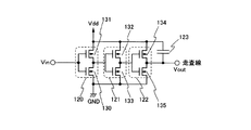
図19に、本実施例の走査線駆動回路が有するバッファ118の構成を示す。バッファ118は、3つのインバータ120〜122で構成されており、インバータ120はnチャネル型TFT130とpチャネル型TFT131を有している。また、インバータ121はnチャネル型TFT132とpチャネル型TFT133を有している。また、インバータ122はnチャネル型TFT134とpチャネル型TFT135を有している。
【0191】
保持容量123が有する2つの電極(容量用第1電極及び容量用第2電極)は、一方には電源電圧Vddが与えられており、もう一方は走査線と電気的に接続されている。
【0192】
図19に示した本実施例のバッファの上面図を、図20(A)に示す。図20(B)は、図20(A)のA−A’における断面図に相当する。電源電圧Vddが供給されている配線143は容量123の容量用第2電極として機能しており、容量123は、容量用第1電極140と、配線143とが、有機樹脂膜145の開口部において、第1無機絶縁膜141及び第2無機絶縁膜142を間に挟んで重なっている部分に形成されている。
【0193】
本実施例は、実施例1と組み合わせて実施することが可能である。
【0194】
(実施例3)
本実施例では、実施例1に示した発光装置とは異なる断面構造を有する発光装置の構成について説明する。
【0195】
図21(A)に示す発光装置は、第2無機絶縁膜7500を形成した後、コンタクトホールを形成する前に透明導電膜を成膜し、パターニングすることで、画素電極7501を形成する。そして、ゲート絶縁膜7502、第1無機絶縁膜7503及び第2無機絶縁膜7500を、有機樹脂膜7504の開口部においてエッチングしてコンタクトホールを形成し、TFT7505と画素電極7501とを電気的に接続する配線7506を形成する。
【0196】
このように、配線7506を形成する前に画素電極7501を形成することで、画素電極の表面を研磨する工程を設けることができる。
【0197】
図21(B)に示す発光装置は、第2無機絶縁膜7510を形成した後、ゲート絶縁膜7512、第1無機絶縁膜7513及び第2無機絶縁膜7510を、有機樹脂膜7514の開口部においてエッチングしてコンタクトホールを形成し、TFT7515と電気的に接続する配線7516を形成する。
【0198】
そして、配線7516と、第2無機絶縁膜7510を覆って、第2の層間絶縁膜7517を形成する。第2の層間絶縁膜7517は、ポジ型の感光性有機樹脂膜でも、ネガ型の感光性有機樹脂膜でも良い。図21(B)では、ポジ型のアクリルを用いて第2の層間絶縁膜7517を形成している。
【0199】
そして第2の層間絶縁膜7517に、露光により開口部を形成して配線7516の一部を露出させる。その後、開口部を覆って、第2の層間絶縁膜7517上に第3の層間絶縁膜7518を形成し、開口部において第3の層間絶縁膜7518を一部除去して配線7516を一部露出させる。このとき、開口部において第2の層間絶縁膜7517が露出しないようにする。
【0200】
そして、第3の層間絶縁膜7518上に透明導電膜を成膜し、パターニングすることで、配線7516に接続された画素電極が形成される。
【0201】
図21(C)に示す発光装置は、第2無機絶縁膜7520上に画素電極7521を形成した後、ネガ型のアクリルを用いて第3の層間絶縁膜7522を形成した例を示している。ネガ型のアクリルを用いて第3の層間絶縁膜7522を形成した場合、第3の層間絶縁膜7522を脱色を目的とした露光をする必要がない。
【0202】
図21(D)では、発光素子の電界発光層の一部に正孔注入層としてポリチオフェン(PEDOT)を用いた場合に、該PEDOT膜をパターニングして除去する例について説明する。
【0203】
ポリチオフェン(PEDOT)は一般的にスピン塗布法を用いて成膜されるため、PEDOTを成膜したくない部分にまで成膜される。そのため、画素電極7530上にPEDOT膜7531を成膜した後、蒸着用のマスクを用いて発光層7532及び陰極7533を蒸着により成膜する。本実施例では発光層としてパラフェニレンビニレン(PPV)膜を用いるが、蒸着法により成膜することができる膜であれば良い。また本実施例では陰極7533としてCaを用いるが、仕事関数の小さい材料で、蒸着法により成膜することができる材料であるならば、用いることができる。
【0204】
次に、陰極7533をマスクとし、酸素プラズマを用いたアッシングによりPEDOTをパターニングする。
【0205】
次に、補助電極7534を形成する。補助電極は、陰極の抵抗を下げるために設ける電極であり、陰極よりも抵抗の低い金属材料からなる。補助電極7534は、陰極よりも抵抗の低い金属材料からなる導電膜を成膜した後パターニングすることで得られる。
【0206】
そして、補助電極7534と陰極7533とを電気的に接続する保護膜7535を、蒸着用のマスクを用いて蒸着により成膜する。保護膜7535は金属材料からなり、陰極7533と同じ材料を用いていても良い。
【0207】
なお図21(D)では、発光素子の陰極をマスクとして、正孔注入層をパターニングする例を示している。しかし、本実施例はこの構成に限定されない。陰極をマスクとして正孔注入層以外の電界発光層をパターニングしても良い。
【0208】
図22(A)に示す発光装置は、第2無機絶縁膜7610を形成した後、陰極よりも抵抗の低い金属材料からなる導電膜を成膜した後、パターニングすることで補助電極7634を形成する。そして、ゲート絶縁膜7612、第1無機絶縁膜7613及び第2無機絶縁膜7610を、有機樹脂膜7614の開口部においてエッチングしてコンタクトホールを形成し、TFT及び補助電極7634と電気的に接続する配線7616を形成する。
【0209】
配線7616はその一部が電界発光層7615と接しており、陰極として機能している。
【0210】
図22(B)に示す発光装置は、第2無機絶縁膜7701上に陰極7700を形成した後、電界発光層7702とITO膜7703を形成する。このときITO膜7703にLiを添加することで、仕事関数を小さくすることができる。そして、Liが添加されたITO膜7703を覆って、別途新たにITO膜7704を成膜する。
【0211】
本実施例は、実施例2と組み合わせて実施することが可能である。
【0212】
(実施例4)
本実施例では、陰極の抵抗を下げるための補助電極と、FPCの端子に接続される入力端子との、電気的な接続について説明する。
【0213】
図23(A)では、開口部を有する第2の層間絶縁膜6200上に、第3の層間絶縁膜6201が形成された後、該第3の層間絶縁膜6201上に補助電極6202が形成された時点での、発光装置の断面図を示す。補助電極6202は、後に形成される陰極よりも配線抵抗の低い材料で形成する。
【0214】
なお、TFTのゲート電極6203と同じ導電膜で形成されたFPC用電極6204は、第2の層間絶縁膜6200の開口部に形成されている。また、FPC用電極6204上に、画素電極6206と同じ透明導電膜で形成された入力端子6205が形成されている。
【0215】
図23(A)の時点では、FPC接続部6205において入力端子6205は、第3の層間絶縁膜6201に覆われている。
【0216】
次に、図23(B)に示すように、第3の層間絶縁膜6201を一部エッチングして除去することで、入力端子6205と、画素電極6206を一部露出させる。このとき、開口部において第2の層間絶縁膜6200が露出しないようにする。
【0217】
そして、画素電極6206上に電界発光層6210と陰極6211を積層した後、入力端子6205と、陰極6211とに接続された保護電極6212を形成する。
【0218】
上記構成では、補助電極6202をエッチングにより形成するとき、第3の層間絶縁膜6201で画素電極6206が覆われているため、画素電極の表面がエッチングにより荒れるのを防ぐことができる。
【0219】
図24に、本実施例の発光装置の、発光素子が形成された基板(素子基板)の上面図を示す。基板830に、画素部831、走査線駆動回路832、信号線駆動回路833、入力端子6205が形成された状態を示している。入力端子6205と各駆動回路、画素部に形成されている電源線及び対向電極は、引き回し配線835で接続されている。発光素子は、ストライプ状にレイアウトされた補助電極6202の間に形成される。
【0220】
また、必要に応じてCPU、メモリーなどを形成したICチップがCOG(Chip on Glass)法などにより素子基板に実装されていても良い。
【0221】
本実施例は、実施例2と自由に組み合わせて実施することが可能である。
【0222】
(実施例5)
本実施例では、本発明の半導体表示装置の1つである液晶表示装置の構成について説明する。
【0223】
図25に本実施例の液晶表示装置の断面図を示す。図25において、絶縁表面上にTFT9001が形成されている。TFT9001はトップゲート型であり、半導体膜9002と、該半導体膜9002と接しているゲート絶縁膜9003と、該ゲート絶縁膜に接しているゲート電極9004とを有している。
【0224】
一方、ゲート絶縁膜9003上に形成されている容量用第1電極9007は、ゲート電極9004と同じ導電膜から形成することができる。
【0225】
そして、TFT9001及び容量用電極9007を覆うように、第1無機絶縁膜9008が形成されている。第1無機絶縁膜9008は、窒素を含む絶縁膜であり、後に形成される有機樹脂膜よりも水分を透過しにくい性質を有している。
【0226】
そして、第1無機絶縁膜上に感光性の有機樹脂を塗布した後、焼成し、開口したい部分を感光して現像することで、開口部を有する有機樹脂膜9009が形成されている。この時点で、開口部において第1無機絶縁膜9008の一部が露出している。
【0227】
そして、有機樹脂膜9009と、開口部において露出している第1無機絶縁膜9008の一部を覆って、第2無機絶縁膜9010を形成する。第2無機絶縁膜9010は、第1無機絶縁膜9008と同様に、窒素を含む絶縁膜であり、後に形成される有機樹脂膜よりも水分を透過しにくい性質を有している。
【0228】
そして、有機樹脂膜9009の開口部において、半導体膜9002の一部を露出させるように、ゲート絶縁膜9003、第1無機絶縁膜9008及び第2無機絶縁膜9010をドライエッチングして、コンタクトホールを形成する。半導体膜9002はエッチングストッパーとしての効果を有している。
【0229】
このとき、容量用第1電極9007上に存在する第1無機絶縁膜9008及び第2無機絶縁膜9010は、エッチングされないように、レジストマスクで覆っておく。
【0230】
そして、コンタクトホールを覆うように、第2無機絶縁膜9010上に導電膜を成膜する。そして、該導電膜をエッチングすることで、半導体膜9002に接続された配線9011と、容量用第2電極9012とが形成される。容量用第2電極9012は、第1無機絶縁膜9008及び第2無機絶縁膜9010を間に挟んで、容量用第1電極9007と重なっている。この、容量用第2電極9012と、第1無機絶縁膜9008及び第2無機絶縁膜9010と、容量用第1電極9007とによって、保持容量9013が形成されている。
【0231】
そして、配線9011及び容量用第2電極9012を覆うように、第2無機絶縁膜9010上に透明導電膜を形成し、パターニングすることで、画素電極9015を形成する。画素電極9015は配線9011の1つと、容量用第2電極9012と接続されている。
【0232】
そして画素電極9015と、配線9011及び容量用第2電極9012とを覆って、第2無機絶縁膜9010上にポジ型のアクリルを塗布し、焼成した後部分的に露光し、現像することで、開口部を有する第3の層間絶縁膜9017を形成する。第3の層間絶縁膜9017は本実施例ではポジ型のアクリル用いたが、ネガ型のアクリルであってもよい。画素電極9015は開口部において露出している。この第3の層間絶縁膜9017は基板間の間隔を一定に保つためのスペーサとして用いる。その厚さは液晶の種類によって変わるが、0.7μm〜数μm程度であることが望ましい。
【0233】
そして、配向膜9018を形成する。通常液晶表示装置の配向膜にはポリイミド樹脂を用いる。配向膜を形成した後、ラビング処理を施して液晶分子がある一定のプレチルト角を持って配向するようにした。
【0234】
対向側の対向基板9020には、遮光膜9021、対向電極9022および配向膜9023を形成する。遮光膜9021はTi膜、Cr膜、Al膜などを150〜300nmの厚さで形成する。そして、画素部と駆動回路が形成された素子基板と対向基板とをシール材9024で貼り合わせる。シール材9024にはフィラー(図示せず)が混入されていて、このフィラーと第3の層間絶縁膜9017によって、均一な間隔を持って2枚の基板が貼り合わせられる。その後、両基板の間に液晶9025を注入する。液晶材料には公知の液晶材料を用いれば良い。例えば、TN液晶の他に、電場に対して透過率が連続的に変化する電気光学応答性を示す、無しきい値反強誘電性混合液晶を用いることもできる。この無しきい値反強誘電性混合液晶には、V字型の電気光学応答特性を示すものもある。このようにして図25に示すアクティブマトリクス型液晶表示装置が完成する。
【0235】
本実施例で示した液晶表示装置は、本発明の液晶表示装置のほんの一例であり、本発明は図25に示した構成に限定されない。
【0236】
なお本実施例は、実施例2と自由に組み合わせることが可能である。
【0237】
(実施例6)
本実施例では、本発明の半導体表示装置の1つである、液晶表示装置の駆動回路の構成について説明する。
【0238】
図26(A)は、本実施例のアクティブマトリクス型液晶表示装置の概略ブロック図である。501は信号線駆動回路、503は走査線駆動回路、504は画素部である。
【0239】
信号線駆動回路501は、シフトレジスト回路501−1、ラッチ回路A501−2、ラッチ回路B501−3、D/A変換回路501−5を有している。その他、バッファやレベルシフト回路(いずれも図示せず)を有している。また、説明の便宜上、DAC501−5にはレベルシフト回路が含まれている。
【0240】
また、503は走査線駆動回路であり、シフトレジスト回路、バッファ、レベルシフタ回路を有していても良い。
【0241】
画素部504は複数の画素を有している。各画素にはスイッチング素子としてのTFTが配置されており、各画素TFTのソースとドレインは、一方が信号線に、もう一方が画素電極に接続されている。また、ゲートは走査線に電気的に接続されている。各画素TFTは、各画素TFTに電気的に接続された画素電極へのビデオ信号の供給を制御している。各画素電極にビデオ信号が供給され、各画素電極と対向電極の間に挟まれた液晶に電圧が印加され液晶が駆動される。
【0242】
まず、信号線駆動回路501の動作を説明する。シフトレジスト回路501−1では、入力されたクロック信号及びスタートパルスに基づいて、デジタルビデオ信号がラッチ回路A501−2にラッチされるタイミングを制御するタイミング信号を生成する。
【0243】
ラッチ回路A(501−2)では、生成されたタイミング信号に同期して、デジタルビデオ信号がラッチされる。ラッチ回路A(501−2)の全てのステージにおいてデジタルビデオ信号がラッチされると、シフトレジスト回路501−1の動作タイミングに合わせて、ラッチ回路B(501−3)にラッチシグナル(Latch Signal)が供給される。この瞬間、ラッチ回路A(501−2)にラッチされているデジタルビデオ信号は、ラッチ回路B(501−3)に一斉に送出され、ラッチ回路B(501−3)の全ステージのラッチ回路にラッチされる。
【0244】
デジタルビデオ信号をラッチ回路B(501−3)に送出し終えたラッチ回路A(501−2)には、シフトレジスト回路501−1からのタイミング信号に基づき、再びデジタルビデオ信号のラッチが順次行われる。
【0245】
一方、ラッチ回路B(501−3)にラッチされているデジタルビデオ信号が、D/A変換回路(DAC)501−5に供給される。DAC501−5は、デジタルビデオ信号をアナログのビデオ信号(アナログビデオ信号)に変換し、各信号線に順次供給する。
【0246】
走査線駆動回路503においては、シフトレジスト回路(図示せず)からのタイミング信号がバッファ(図示せず)に供給され、対応する走査線(走査線)に供給される。走査線には、1ライン分の画素TFTのゲート電極が接続されており、1ライン分全ての画素TFTを同時にONにしなくてはならないので、バッファには電流容量の大きなものが用いられる。
【0247】
このように、走査線駆動回路からの走査信号によって対応する画素TFTのスイッチングが行われ、信号線駆動回路からのアナログビデオ信号(階調電圧)が画素TFTに供給され、液晶分子が駆動される。
【0248】
本実施例の液晶表示装置において、D/A変換回路501−5が容量分割型の場合、実施の形態で示した構成の容量を有していても良い。
【0249】
なお本実施例で示した信号線駆動回路と走査線駆動回路は、液晶表示装置の駆動回路として用いられているが、発光装置やその他の半導体表示装置の駆動回路として用いても良い。
【0250】
(実施例7)
本発明の半導体表示装置は、様々な電子機器への適用が可能である。その一例は、携帯情報端末(電子手帳、モバイルコンピュータ、携帯電話等)、ビデオカメラ、デジタルカメラ、パーソナルコンピュータ、テレビ受像器、携帯電話、投影型表示装置等が挙げられる。それら電子機器の具体例を図27に示す。
【0251】
図27(A)は表示装置であり、筐体2001、支持台2002、表示部2003、スピーカー部2004、ビデオ入力端子2005等を含む。本発明の半導体表示装置を表示部2003に用いることで、本発明の表示装置が完成する。なお、表示装置は、パソコン用、TV放送受信用、広告表示用などの全ての情報表示用表示装置が含まれる。
【0252】
図27(B)はデジタルスチルカメラであり、本体2101、表示部2102、受像部2103、操作キー2104、外部接続ポート2105、シャッター2106等を含む。本発明の半導体表示装置を表示部2102に用いることで、本発明のデジタルスチルカメラが完成する。
【0253】
図27(C)はノート型パーソナルコンピュータであり、本体2201、筐体2202、表示部2203、キーボード2204、外部接続ポート2205、ポインティングマウス2206等を含む。本発明の半導体表示装置を表示部2203に用いることで、本発明のノート型パーソナルコンピュータが完成する。
【0254】
図27(D)はモバイルコンピュータであり、本体2301、表示部2302、スイッチ2303、操作キー2304、赤外線ポート2305等を含む。本発明の半導体表示装置を表示部2302に用いることで、本発明のモバイルコンピュータが完成する。
【0255】
図27(E)は記録媒体を備えた携帯型の画像再生装置(具体的にはDVD再生装置)であり、本体2401、筐体2402、表示部A2403、表示部B2404、記録媒体(DVD等)読み込み部2405、操作キー2406、スピーカー部2407等を含む。表示部A2403は主として画像情報を表示し、表示部B2404は主として文字情報を表示する。なお、記録媒体を備えた画像再生装置には家庭用ゲーム機器なども含まれる。本発明の半導体表示装置を表示部A、B2403、2404に用いることで、本発明の画像再生装置が完成する。
【0256】
図27(F)はゴーグル型ディスプレイ(ヘッドマウントディスプレイ)であり、本体2501、表示部2502、アーム部2503を含む。本発明の半導体表示装置を表示部2502に用いることで、本発明のゴーグル型ディスプレイが完成する。
【0257】
図27(G)はビデオカメラであり、本体2601、表示部2602、筐体2603、外部接続ポート2604、リモコン受信部2605、受像部2606、バッテリー2607、音声入力部2608、操作キー2609等を含む。本発明の半導体表示装置を表示部2602に用いることで、本発明のビデオカメラが完成する。
【0258】
ここで図27(H)は携帯電話であり、本体2701、筐体2702、表示部2703、音声入力部2704、音声出力部2705、操作キー2706、外部接続ポート2707、アンテナ2708等を含む。なお、表示部2703は黒色の背景に白色の文字を表示することで携帯電話の消費電流を抑えることができる。本発明の半導体表示装置を表示部2703に用いることで、本発明の携帯電話が完成する。
【0259】
以上の様に、本発明の適用範囲は極めて広く、あらゆる分野の電子機器に用いることが可能である。また、本実施例は実施例1〜6に示したいずれの構成とも組み合わせて実施することが可能である。
【0260】
(実施例8)
図31(A)に示す写真は、非感光性アクリル膜(膜厚:約1.3μm)に対してドライエッチング処理を施してパターン化した状態の断面SEM(走査型電子顕微鏡)写真であり、図31(B)はその模式図である。従来のように非感光性アクリル膜に対してドライエッチング処理を施した場合、パターン上部に曲面は殆ど形成されず、実質的に曲率半径(R)のない上端部となる。また、パターンの下部は、テーパー角(接触角)が約63°となっているが、この下端部においても曲面は観察されない。
【0261】
次に、図32(A)に示す写真は、ポジ型感光性アクリル膜(膜厚:約2.0μm)に対して露光及び現像処理を施してパターン化した状態の断面SEM写真であり、図32(B)はその模式図である。ポジ型感光性アクリル膜の断面形状については、現像液によるエッチング処理後において非常になだらかな曲面を有し、連続的に曲率半径(R)が変化している。また、接触角も約32〜33°と小さな値が得られている。即ち、図1(B)に示した形状そのままであり、本発明の薄膜トランジスタ及び半導体表示装置を作製するにあたって、非常に有用な形状と言える。勿論、接触角の値はエッチング条件や膜厚等によって変わるが、前掲のように30°<θ<65°を満たせば良い。
【0262】
次に、図33(A)に示す写真は、ネガ型感光性アクリル膜(膜厚:約1.4μm)に対して露光及び現像処理を施してパターン化した状態の断面SEM写真であり、図33(B)はその模式図である。ネガ型感光性アクリル膜の断面形状については、現像液によるエッチング処理後においてなだらかなS字状の曲面を形成し、パターン上端部においてはある曲率半径(R)をもって湾曲している。また、接触角は約47°という値が得られている。この場合、図33(B)のWで表すテール(裾)の部分の長さが問題となる。特に、微細加工の必要なコンタクトホール(開口部)においては、このテール部分が長くなってしまうと、コンタクトホール内で下層の電極もしくは配線が露出しない状況が発生する恐れがあり、接触不良による断線が懸念される。ただし、このテール部分の長さ(W)が1μm以下(好ましくは、コンタクトホールの半径未満の長さ)であれば、そのような断線の可能性は低くなる。
【0263】
次に、図34(A)に示す写真は、ポジ型感光性ポリイミド膜(膜厚:約1.5μm)に対して露光及び現像処理を施してパターン化した状態の断面SEM写真であり、図34(B)はその模式図である。ポジ型感光性ポリイミド膜の断面形状については、現像液によるエッチング処理後において若干のテール部分(長さWで表される。)と湾曲した上端部を有しているが、その曲率半径(R)は小さい。
【0264】
以上の断面形状を観察してみると、次のような考察をすることができる。コンタクトホール(開口部)形成後、電極もしくは配線となる金属膜を成膜する際、スパッタ法、蒸着法もしくはCVD法等が用いられる。薄膜を構成する材料分子は、被形成面に付着すると安定なサイトを求めて表面を移動するが、コンタクトホールの上端部の如き鋭角をもった形状(凸部となる形状)の部分に集まりやすいことが知られている。この傾向は、特に蒸着法において顕著である。そのため、開口部の断面形状が図31(A)に示したような形状であると、開口部の縁に材料分子が集中してしまうため、その部分だけ局部的に膜厚が厚くなり、ひさし状の凸部を形成してしまう。これが後に断線(段切れ)等の不良の原因となるため、好ましいものではない。従って、図31(A)に示した非感光性アクリル膜及び図34(A)に示したポジ型感光性ポリイミド膜は、被覆率(カバレッジ)の観点から不利な材料と言える。
【0265】
また、前掲の図33(A)、図34(A)ように、コンタクトホールの下端部においてテール部分が形成されるような形状は、場合によってはテール部分がコンタクトホールの底面を覆ってしまい、接触不良を招く恐れがあるため、接触性の観点から不利な材料と言える。勿論、テール部分の長さが1μm以下(好ましくは、コンタクトホールの半径未満の長さ)であれば問題はない。
【0266】
(実施例9)
本実施例では、本発明の半導体表示装置の作製方法について説明する。なお本実施例では、FPCが接続される部分(FPC接続部)9200と、容量用第1電極9222と、画素部9220と、保護回路9201の一部について、各工程における断面構造を示す。
【0267】
まず、基板上にTFT9202と、ゲート絶縁膜9204上に引き回し配線9221とを形成する。TFT9202は半導体膜9203と、該半導体膜9203に接しているゲート絶縁膜9204と、該ゲート絶縁膜9204に接しているゲート電極9205とを有している。引き回し配線9221及び容量用第1電極9222は、ゲート電極9205と同じ導電膜から形成されている。
【0268】
なお本実施例ではゲート絶縁膜9204としてSiONを用いる。ゲート絶縁膜の成膜方法及びその膜厚については、実施例1の記載を参照することができる。
【0269】
そして、該引き回し配線9221、容量用第1電極9222及びTFT9202を覆って、第1無機絶縁膜9206が成膜されている。本実施例では第1無機絶縁膜9206としてSiNを用いる。第1無機絶縁膜9206の成膜方法及びその膜厚については、実施例1の記載を参照することができる。
【0270】
そして、本実施例では第1無機絶縁膜9206を覆って、バリア膜9207を成膜する(図35(A))。バリア膜9207は、本実施例ではSiO2を用いる。本実施例ではバリア膜9207をCVD法を用いて30nm〜120nm程度の厚さに成膜する。
【0271】
次に、バリア膜9207上に有機樹脂を塗布し、部分的に露光した後、現像することで、開口部を有する有機樹脂膜9208を形成する(図35(B))。なお実施例1で記載したように、部分的に露光した後、現像する前に全体を露光することで、有機樹脂膜9208を脱色するようにしても良い。
【0272】
次に、有機樹脂膜9208をマスクとして、SiO2からなるバリア膜9207をウエットエッチングする。なお本実施例では、フッ酸系のエッチャントを用いて、20℃においてウエットエッチングを行い、有機樹脂膜9208の開口部においてバリア膜9207を除去し、機樹脂膜9208の開口部において第1無機絶縁膜9206を露出させる(図35(C))。
【0273】
次に、開口部を覆うように有機樹脂膜9208上にSiNからなる第2無機絶縁膜9209を成膜する。なお、第2無機絶縁膜9209の膜厚及びその成膜方法については、実施例1の記載を参照することができる。
【0274】
そして、有機樹脂膜9208の開口部において、第1無機絶縁膜9206、第2無機絶縁膜9209及びゲート絶縁膜9204をドライエッチングすることで、コンタクトホールを形成する。該コンタクトホールにおいて、引き回し配線9221及び半導体膜9203の不純物領域9225、9226の一部が露出する。このとき、容量用第1電極9222が露出しないように、エッチングの際にマスクで覆っておく。
【0275】
そして、コンタクトホールを覆って、第2無機絶縁膜9209上に導電膜を成膜し、パターニングすることで、引き回し配線9221に接する引き出し用配線9210と、半導体膜9203の不純物領域9226に接する配線9211と、有機樹脂膜9208の開口部において、第1無機絶縁膜9206及び第2無機絶縁膜9209を間に挟んで容量用第1電極9222と重なっている容量用第2電極9212が形成される。
【0276】
そして、透明導電膜を成膜してパターニングすることで、コンタクトホールにおいて引き回し配線9221に接する入力端子9213と、配線9211に接する画素電極9214が形成される。
【0277】
SiO2で形成されているバリア膜9207よりも、SiNで形成されている第1無機絶縁膜9206の方が電気伝導度が高いため、コンタクトホールの形成のためにドライエッチングを行なうことでプラズマ雰囲気化に曝されても、ゲート絶縁膜9204にホールがトラップされる所謂チャージングダメージを防ぐことができ、TFTの閾値がプラス側へばらつくのを防ぐことができる。
【0278】
本実施例は、実施例1〜8と自由に組み合わせて実施することが可能である。
【0279】
(実施例10)
本実施例では、本発明の半導体表示装置の作製方法において、第1及び第2無機絶縁膜にコンタクトホールを形成した後の、工程順序のバリエーションについて説明する。
【0280】
図37(A)では、FPC接続部9100においてゲート絶縁膜9103上に引き回し配線9104が形成されている。また画素部9120においてTFT9101が形成されている。TFT9101は半導体膜9102と、半導体膜9102に接するゲート絶縁膜9103と、ゲート絶縁膜9103に接するゲート電極9121とを有している。そして引き回し配線9104及びTFT9101を覆って、第1無機絶縁膜9105が形成されており、第1無機絶縁膜9105上に開口部を有する有機樹脂膜9106が形成されている。さらに開口部を覆って有機樹脂膜9106上に第2無機絶縁膜9107が形成されている。
【0281】
そして、有機樹脂膜9106の開口部において、第1無機絶縁膜9105及び第2無機絶縁膜9107にコンタクトホールが形成されている。コンタクトホールにおいて、引き回し配線9104及び半導体膜9102が有する不純物領域の一部が露出している。
【0282】
次に図37(B)に示すように、コンタクトホールを覆って、第2無機絶縁膜9107上に透明導電膜9108を成膜する。
【0283】
そして、図37(C)に示すように透明導電膜9108をパターニングして、コンタクトホールにおいて引き回し配線9104に接する入力端子9109と、画素電極9110とを形成する。
【0284】
次に、導電膜を成膜し、パターニングすることで、コンタクトホールにおいて引き回し配線9104に接する引き出し用配線9111と、半導体膜9102の不純物領域及び画素電極に接する配線9112が形成される。
【0285】
なお図37では、透明導電膜9108または画素電極9110の表面を研磨する工程が設けられる。表面研磨は透明導電膜9108を成膜後、パターニングする前、つまり図37(B)と図37(C)の間に設けることができる。また、表面研磨を、パターニングによる画素電極9110の形成後、配線を形成する前、つまり図37(C)と図37(D)の間に設けることができる。上記表面研磨により、配線が形成される前なので、透明導電膜9108または画素電極9110の表面のみを研磨することができる。
【0286】
また、表面研磨を、配線9112形成後、つまり図37(D)の後に設けることができる。上記表面研磨により、透明導電膜または画素電極の研磨により生じた微細な粒子がコンタクトホール内に入り込むのを防ぐことができ、コンタクト不良が生じるのを防ぐことができる。
【0287】
次に、本発明の半導体表示装置の作製方法において、図37で示したのとは異なる順序の作製工程について説明する。
【0288】
図38(A)では、FPC接続部9000においてゲート絶縁膜9003上に引き回し配線9004が形成されている。また画素部9020においてTFT9001が形成されている。TFT9001は半導体膜9002と、半導体膜9002に接するゲート絶縁膜9003と、ゲート絶縁膜9003に接するゲート電極9021とを有している。そして引き回し配線9004及びTFT9001を覆って、第1無機絶縁膜9005が形成されており、第1無機絶縁膜9005上に開口部を有する有機樹脂膜9006が形成されている。さらに開口部を覆って有機樹脂膜9006上に第2無機絶縁膜9007が形成されている。
【0289】
そして、有機樹脂膜9006の開口部において、第1無機絶縁膜9005及び第2無機絶縁膜9007にコンタクトホールが形成されている。コンタクトホールにおいて、引き回し配線9004及び半導体膜9002が有する不純物領域の一部が露出している。
【0290】
そして、図38(B)に示すように、コンタクトホールを覆うように導電膜を成膜した後、パターニングすることで、コンタクトホールにおいて引き回し配線9004に接する引き出し用配線9011と、半導体膜9002の不純物領域に接する配線9008が形成される。
【0291】
次に、図38(C)に示すように、透明導電膜9010を成膜する。透明導電膜9010はコンタクトホールにおいて引き回し配線9004に接している。また透明導電膜9010は、配線9008と接している。
【0292】
次に図38(D)に示すように、透明導電膜9010をパターニングして、引き回し配線9004に接する入力端子9012と、配線9008に接する画素電極9013とが形成される。
【0293】
なお本実施例では、透明導電膜9010または画素電極9013の表面を研磨する工程が設けられる。表面研磨は透明導電膜9010を成膜後、パターニングする前、つまり図38(C)と図38(D)の間に設けることができる。また、表面研磨を、パターニングによる画素電極9013の形成後、つまり図38(D)の後に設けることができる。上記表面研磨により、透明導電膜または画素電極の研磨により生じた微細な粒子がコンタクトホール内に入り込むのを防ぐことができ、コンタクト不良が生じるのを防ぐことができる。
【0294】
なお、アクリル樹脂膜上にITO膜を成膜した場合、ITO膜を研磨するとITO膜がアクリル樹脂膜から剥離する場合があった。しかし、間に無機絶縁膜を介してITO膜を成膜すると、研磨によるITO膜の剥離が抑えられる。
【0295】
本実施例は、実施例1〜9と自由に組み合わせて実施することが可能である。
【0296】
【発明の効果】
有機樹脂膜を無機絶縁膜で覆うことで、ドライエッチングによる表面の荒れを抑えることができる。よって、後に形成される画素電極等の表面に凹凸が現れたり、画素電極の厚さが不均一になったりするのを防ぐことができるので、表示にむらが生じるのを防ぐことができる。
【0297】
また有機樹脂膜を、該有機樹脂と比較して水分を透過させにくい窒素を含む無機絶縁膜で覆うことで、有機樹脂膜からの水分の放出を抑えることができ、また逆に有機樹脂が水分を含んで膨潤するのを防ぐことができる。よって、配線が有機樹脂膜から放出される水分により腐食するのを防ぐことができる。さらに、有機発光素子(OLED:Organic Light Emitting Diode)に代表される発光素子を用いた発光装置の場合、有機樹脂膜から放出される水分により発光素子の輝度が劣化するのを防ぐことができる。
【0298】
さらに、有機樹脂膜が露出しないように無機絶縁膜で全体を覆ってしまうことで、現像の際に用いられるアルカリ性の水溶液中の水分を含んで膨潤するのを防ぐことができ、現像後の水分除去を目的とした加熱処理の処理時間を抑えることができる。さらに、有機樹脂膜中の水分が隣接する膜または電極に放出されるのをより防ぐことができ、長期的なパネルの信頼性を高めることができる。
【0299】
また、非感光性の有機樹脂を用いた場合、層間絶縁膜に開口を形成するためには一般的にドライエッチングが用いられる。ドライエッチングは活性なラジカルや反応性ガスのプラズマを用いたエッチング法である。層間絶縁膜はゲート絶縁膜の10倍程度の厚さを有しているため、開口を目的としたドライエッチングに時間がかかる。TFTの形成された基板がプラズマに曝されている時間が長いと、ゲート絶縁膜にホールがトラップされる所謂チャージングダメージにより、TFTの閾値がプラス側へバラツキやすくなる。よって本発明のように感光性の有機樹脂を用いて、ウェットエッチングにより開口を形成することで、ドライエッチングを用いる時間を大幅に削減することができ、TFTの閾値のバラツキを抑えることができる。
【0300】
また、静電気の放電による劣化あるいは破壊から半導体素子を保護したり、ノイズによる半導体素子の誤作動を防いだりするための保護回路が有する容量を上記保持容量で形成する。上記構成により、保護回路を画素部と同じ基板上に容易に作りこむことができ、また、静電気により半導体素子が劣化または破壊されたり、ノイズにより誤作動したりするのを防ぐことができる。
【図面の簡単な説明】
【図1】 開口部における感光性アクリル膜の断面図。
【図2】 開口部における感光性ポジ型ポリイミド膜の断面図。
【図3】 コンタクトホールの断面図。
【図4】 コンタクトホールと配線との位置関係を示す図。
【図5】 本発明の半導体表示装置が有するTFTと保持容量の断面図。
【図6】 本発明の半導体表示装置の駆動回路のブロック図。
【図7】 保護回路の回路図。
【図8】 保護回路の動作を示す図。
【図9】 クロック信号のタイミングチャート。
【図10】 保護回路の回路図。
【図11】 保護回路のマスク図面。
【図12】 保護回路が有する保持容量の断面図。
【図13】 本発明の半導体表示装置の作製方法を示す図。
【図14】 本発明の半導体表示装置の作製方法を示す図。
【図15】 本発明の半導体表示装置の作製方法を示す図。
【図16】 本発明の半導体表示装置の作製方法を示す図。
【図17】 本発明の半導体表示装置の作製方法を示す図。
【図18】 本発明の半導体表示装置の構成を示すブロック図と画素部の回路図。
【図19】 バッファと走査線と保持容量の回路図。
【図20】 バッファと保持容量のマスク図面と、該保持容量の断面図。
【図21】 本発明の半導体表示装置の断面図。
【図22】 本発明の半導体表示装置の断面図。
【図23】 本発明の半導体表示装置の作製方法を示す図。
【図24】 本発明の半導体表示装置の上面図。
【図25】 本発明の半導体表示装置の断面図。
【図26】 本発明の半導体表示装置の駆動回路のブロック図。
【図27】 本発明の半導体表示装置を用いた電子機器の図。
【図28】 本発明の半導体表示装置の断面図。
【図29】 TFTのチャネル長と閾値の関係を示す図。
【図30】 TFTのCV特性を示す図。
【図31】 開口部における非感光性アクリル膜の断面図。
【図32】 開口部におけるポジ型感光性アクリル膜の断面図。
【図33】 開口部におけるネガ型感光性アクリル膜の断面図。
【図34】 開口部におけるポジ型感光性ポリイミド膜の断面図。
【図35】 本発明の半導体表示装置の作製方法を示す図。
【図36】 本発明の半導体表示装置の作製方法を示す図。
【図37】 本発明の半導体表示装置の作製方法を示す図。
【図38】 本発明の半導体表示装置の作製方法を示す図。[0001]
BACKGROUND OF THE INVENTION
The present invention relates to a semiconductor display device using an organic resin film as an interlayer insulating film, and more particularly to a semiconductor display device configured to protect internal circuits from destruction due to a high voltage load such as static electricity by providing a protective circuit in an input / output unit. About.
[0002]
[Prior art]
In recent years, technology for forming TFTs on a substrate has greatly advanced, and application development to an active matrix semiconductor display device which is one of semiconductor devices has been advanced. In particular, a TFT using a polycrystalline semiconductor film has higher field effect mobility (also referred to as mobility) than a TFT using a conventional amorphous semiconductor film, and thus can operate at high speed. For this reason, it is possible to perform control of a pixel, which has been conventionally performed by a drive circuit provided outside the substrate, with a drive circuit formed on the same substrate as the pixel.
[0003]
The TFT includes an active layer obtained by adding an impurity imparting one conductivity type to a semiconductor film, a gate electrode, and a gate insulating film provided between the active layer and the gate electrode. In general, an interlayer insulating film made of an insulating film is formed so as to cover the TFT, and a wiring electrically connected to the TFT is formed on the interlayer insulating film.
[0004]
If the surface of the interlayer insulating film is not sufficiently flattened, when a wiring electrically connected to the TFT is formed on the interlayer insulating film, the wiring is disconnected or the wiring is partially thinned. This can increase the wiring resistance. In addition to wiring, when a pixel electrode is formed on an interlayer insulating film, the surface of the pixel electrode cannot be made uneven due to the unevenness of the surface of the interlayer insulating film, or the thickness of the pixel electrode cannot be made uniform. Or it may appear uneven on the display.
[0005]
Therefore, it is necessary to make the interlayer insulating film sufficiently thick, for example, about 1 to 5 μm so that unevenness does not appear on the surface of the interlayer insulating film due to the shape of the TFT.
[0006]
The interlayer insulating film is roughly classified into an inorganic insulating film (hereinafter referred to as an inorganic insulating film) and an insulating film made of an organic resin having an insulating property (hereinafter referred to as an organic resin film).
[0007]
The inorganic insulating film is formed using a vapor phase growth method such as a CVD method or a sputtering method. Therefore, in the case where the inorganic insulating film is an interlayer insulating film, the vapor deposition method must be used to form a film thick enough to flatten the surface.
[0008]
On the other hand, in the case where an organic resin film is used, a film can be formed by applying an organic resin to a substrate on which a TFT is formed. Therefore, an interlayer insulating film having a flat surface can be easily formed.
[0009]
[Problems to be solved by the invention]
Incidentally, the wiring connected to the TFT is formed by forming a conductive film (hereinafter referred to as a conductive film) on an interlayer insulating film having contact holes and etching the conductive film.
[0010]
At this time, the conductive film can be etched by either wet etching or dry etching. However, since wet etching is isotropic etching, it cannot cope with the miniaturization of a wiring pattern of 3 μm or less. On the other hand, since dry etching can perform anisotropic etching, it can cope with miniaturization of wiring patterns.
[0011]
However, the problem with dry etching is that when the conductive film on the interlayer insulating film made of an organic resin film is dry etched, the surface of the organic resin film becomes rough. When the surface of the organic resin film becomes rough, the flatness of the surface of the pixel electrode formed on the organic resin film is impaired, which affects the display of the pixel.
[0012]
In addition, since the organic resin has high water absorption and swells by containing water in an alkaline aqueous solution used for development, it is necessary to provide a step of heating the film to remove the water in the film after development. Furthermore, even if moisture is removed by heat treatment, moisture in the adjacent film and the atmosphere is absorbed, and the moisture in the film corrodes the wiring formed in contact with the organic resin film over time, Long-term panel reliability can be compromised.
[0013]
In view of the above problems, the present invention can obtain flatness of the surface while suppressing the film formation time, can reduce the processing time of the heat treatment for the purpose of removing moisture, and moisture in the interlayer insulating film is adjacent. It is an object of the present invention to provide a semiconductor display device having an interlayer insulating film that can be prevented from being released to a film or an electrode.
[0014]
Further, the fact that the threshold voltage (Vth) of a completed thin film transistor varies greatly when a contact hole is formed by dry etching using a resin film as an interlayer insulating film has been found by the applicant's research. . For example, the data shown in FIG. 29 is a result of examining variation in threshold voltage of a thin film transistor formed over an SOI substrate. Black circles in the figure indicate a case where a laminated structure of a silicon nitride film (SiN) and an acrylic film is used as an interlayer insulating film, and white triangles in the figure indicate a silicon nitride oxide film (SiNO) as an interlayer insulating film. The case where a stacked structure of a silicon oxynitride film (SiON) is used is shown. In any case, a dry etching technique is used for opening the contact hole. The difference between “SiNO” and “SiON” is used in the sense that the former has more atomic% of nitrogen than oxygen and the latter has more atomic% of oxygen than nitrogen.
[0015]
The data in FIG. 29 is a graph in which variation in threshold voltage is evaluated by statistical processing. The horizontal axis represents channel length (carrier movement length), and the vertical axis represents Vth variation. In recent years, “quartile deviation” is known as statistical processing. The quartile deviation is a difference between a value of 25% and a value of 75% in the normal probability graph, and is attracting attention as a statistical process that is not affected by an abnormal value. Based on this quartile deviation (also referred to as 25% quartile deviation), the applicant defines the difference between the 16% value and the 84% value as the 16% quartile deviation, and the value is defined as “Vth”. The variation is plotted on the vertical axis. Since the 16% quantile corresponds to ± σ in the normal probability distribution, a value that can be regarded as ± 3σ by multiplying each coefficient is used in the data plot. As far as the same data is seen, the difference is about 4 times for the n-channel TFT and about 2 times for the p-channel TFT when the acrylic film is used for the interlayer insulating film. The variation is larger. The present applicant presumes that plasma damage during dry etching causes the acrylic film to trap charges, and as a result, the threshold voltage varies.
[0016]
The present invention has been made in view of the above-described problems, and in manufacturing a semiconductor display device using an organic resin film as an interlayer insulating film, a technique for manufacturing a thin film transistor without varying its threshold voltage. It is an object of the present invention to improve the stability of the operation performance of a display device and to increase the design margin in circuit design. Another object is to improve the image quality of the display device.
[0017]
[Means for Solving the Problems]
In the present invention, the periphery of the organic resin film containing a positive photosensitive acrylic resin is surrounded by an insulating film containing nitrogen that is less permeable to moisture than the organic resin.
[0018]
Specifically, after the TFT is formed, an inorganic insulating film containing nitrogen, which is less permeable to moisture than an organic resin, is formed so as to cover the TFT. Next, an organic resin containing a photosensitive acrylic resin is applied, and the film is opened by partially exposing the film. After that, an inorganic insulating film containing nitrogen is formed to cover the opened organic resin film so that moisture is less permeable than the organic resin. Then, in the opening portion of the organic resin film, the gate insulating film and the two layers of the inorganic insulating film containing nitrogen are partially opened by etching to expose the active layer of the TFT.
[0019]
At the time of this etching, the organic resin film should not be exposed in a region where a portion where it is desired to avoid the influence of moisture and the unevenness of the surface, such as wiring or pixel electrodes, is formed on the surface in a later step. It is essential. In other regions, it may be completely covered with an inorganic insulating film.
[0020]
In general, an inorganic insulating film has less surface roughness because it has less etching damage due to dry etching than an organic resin film typified by an acrylic resin. Accordingly, unevenness appears on the surface of a pixel electrode or the like to be formed later, or the thickness of the pixel electrode is not uniform, so that uneven display can be prevented.
[0021]
In addition, by covering the organic resin film with an inorganic insulating film containing nitrogen that is less permeable to moisture than the organic resin, the release of moisture from the organic resin film can be suppressed, and conversely, Can be prevented from swelling. Therefore, the wiring can be prevented from being corroded by moisture released from the organic resin film. Furthermore, in the case of a light-emitting device using a light-emitting element typified by an organic light-emitting element (OLED: Organic Light Emitting Diode), the luminance of the light-emitting element can be prevented from being deteriorated by moisture released from the organic resin film.
[0022]
Furthermore, by covering the whole with an inorganic insulating film so that the organic resin film is not exposed, it is possible to prevent swelling including moisture in an alkaline aqueous solution used during development, and moisture after development. The processing time of the heat treatment for the purpose of removal can be suppressed. Furthermore, it is possible to further prevent moisture in the organic resin film from being released to an adjacent film or electrode, and to improve long-term panel reliability.
[0023]
In the present invention, a photosensitive acrylic resin is used as the organic resin film. The photosensitive organic resin includes a positive type in which a portion exposed to energy rays such as light, electrons, and ions is removed, and a negative type in which the exposed portion remains. FIG. 1 is a cross-sectional view of an opening of a positive acrylic resin and an opening of a negative acrylic resin.
[0024]
In the case of a positive acrylic resin, as shown in FIG. 1A, after forming the first inorganic insulating
[0025]
FIG. 1B shows an enlarged view of a cross section of the opened positive type
[0026]
In the case where positive acrylic is used, the angle θ with respect to the substrate of the contact point of the opening where the positive
[0027]
As described above, in the case of a positive type organic resin film, the center of curvature of the surface of the organic resin film in the opening portion is all on the substrate side, and a part of the film is hardly left in a portion where the opening is desired due to etching failure. Therefore, contact failure is unlikely to occur, leading to an improvement in yield.
[0028]
In the case of a negative acrylic resin, as shown in FIG. 1C, after forming the first inorganic insulating
[0029]
FIG. 1D shows an enlarged view of a cross section of the opened negative
[0030]
As described above, in the case of a negative organic resin film, the center of curvature of the surface of the organic resin film in the opening portion exists on the side opposite to the substrate from the contact R0 toward the center. The longer the distance from the contact R0 to the point where the negative
[0031]
However, the organic resin that can form the cross-sectional shape shown in FIGS. 1A and 1B is still more organic than the organic resin that forms the cross-sectional shape shown in FIGS. It is preferable to be used as a part of the interlayer insulating film. However, not all positive photosensitive organic resins can form the cross-sectional shapes shown in FIGS. 1 (A) and 1 (B). Positive type acrylic can form the cross-sectional shape shown in FIGS. 1A and 1B, but positive type polyimide cannot be formed.
[0032]
When a non-photosensitive organic resin is used, dry etching is generally used to form an opening in the interlayer insulating film. Dry etching is an etching method using plasma of active radicals or reactive gases. Since the interlayer insulating film has a thickness about 10 times that of the gate insulating film, it takes time for dry etching for the purpose of opening, and the object to be processed is exposed to the plasma for a longer time. If the substrate on which the TFT is formed is exposed to plasma for a long time, the threshold value of the TFT is likely to vary to the plus side due to so-called charging damage in which holes are trapped in the gate insulating film. Therefore, by using a photosensitive organic resin as in the present invention to form an opening by wet etching, the time for using dry etching can be significantly reduced, and variations in the threshold value of the TFT can be suppressed.
[0033]
In the present invention, the gate electrode of the TFT and the electrode of the capacitor used in the drive circuit of the semiconductor display device are simultaneously formed, and the wiring electrically connected to the TFT and the other electrode of the capacitor are formed. Form at the same time. Then, in the opening of the organic resin film, a two-layer inorganic insulating film is sandwiched between two electrodes and overlapped to form a storage capacitor.
[0034]
The semiconductor display device of the present invention has a protection circuit using the storage capacitor.
[0035]
Static electricity generated by friction or the like can be a high voltage ranging from several tens of volts to sometimes several tens of kV. When a charged person or object comes into contact with the semiconductor display device, the charge may be discharged at once in a short time of about several μs to several ms through the input terminal, wiring, or circuit of the semiconductor display device. When such a sudden discharge occurs, a semiconductor element such as a TFT having a very thin gate insulating film and a very short channel length used in a circuit in the semiconductor display device is deteriorated or destroyed. .
[0036]
In addition, a clock signal or the like given to the input terminal of the semiconductor display device may contain noise at a certain frequency. Due to this noise, a voltage higher or lower than the desired voltage is momentarily applied to the semiconductor element, which may cause malfunction of the semiconductor element. In particular, in the case of a semiconductor display device, the noise may cause image disturbance.
[0037]
In the present invention, a capacitor included in a protection circuit for protecting a semiconductor element from deterioration or destruction due to electrostatic discharge or preventing a malfunction of the semiconductor element due to noise is formed by the holding capacitor. With the above structure, the protection circuit can be easily built on the same substrate as the pixel portion, and the semiconductor element is prevented from being deteriorated or destroyed by static electricity or malfunctioning due to noise, thereby disturbing the image. Can be prevented.
[0038]
DETAILED DESCRIPTION OF THE INVENTION
FIG. 2 shows an enlarged view of a cross section in the opening when positive photosensitive polyimide is used. As in the case of using positive acrylic, as shown in FIG. 2, after forming the first inorganic insulating film, positive polyimide is formed. Then, the opening is exposed and developed to form an opening, and the first inorganic insulating
[0039]
Since the
[0040]
Therefore, as shown in FIG. 2, positive photosensitive polyimide or other organic resin that forms a cross-sectional shape in which the end of the opening does not draw a curve is used as a part of the interlayer insulating film of the present invention. Is not preferred.
[0041]
Next, a cross section near the contact hole when the contact hole is formed by etching and opening the inorganic insulating film will be described. After forming the state shown in FIG. 1A, a resist
[0042]
Note that FIG. 3B illustrates a state in the vicinity of the contact hole viewed from the top surface of the substrate, and illustrates a state after the resist
[0043]
The
[0044]
FIG. 4 shows a positional relationship between the wiring, the
[0045]
A
[0046]
In this manner, the
[0047]
4A and 4B, the
[0048]
FIG. 4C is a top view of the vicinity of the
[0049]
A
[0050]
Although FIG. 4 shows the contact between the wiring and the semiconductor film, the same applies to the contact between the wiring and the gate electrode.
[0051]
Next, the structure of the TFT and the capacitor in the semiconductor display device of the present invention will be described with reference to FIG.
[0052]
In FIG. 5A, a
[0053]
On the other hand, the capacitor
[0054]
A first inorganic insulating
[0055]
An
[0056]
Then, a second inorganic insulating
[0057]
Note that the first inorganic insulating
[0058]
Then, the
[0059]
At this time, the first inorganic insulating
[0060]
Then, the resist mask is removed with a developer. As the developer, an alkaline aqueous solution is generally used and contains a large amount of water. In the present invention, since the
[0061]
Then, a conductive film is formed over the second inorganic insulating
[0062]
The present invention is characterized in that the
[0063]
In the opening of the
[0064]
Note that the
[0065]
Note that a storage capacitor may be formed between the semiconductor film and the capacitor
[0066]
A so-called dual gate TFT in which two gate electrodes overlap with a channel formation region interposed therebetween may be used. FIG. 28B is a cross-sectional view of a semiconductor device using a dual gate TFT. The
[0067]
By applying the same voltage to the first gate electrode and the second gate electrode, the depletion layer spreads quickly as if the film thickness of the semiconductor film was substantially reduced, so that the subthreshold coefficient (S value) Can be reduced, and the on-current can be increased. Furthermore, interface scattering can be suppressed and transconductance (gm) can be increased. In addition, by applying a common voltage to the first or second gate electrode, variation in threshold value can be suppressed as compared with the case where there is one electrode, and off current can be suppressed.
[0068]
A first
[0069]
The second electrode for
[0070]
FIG. 5B shows the structure of the semiconductor display device of the present invention in the case where the TFT is a bottom gate.
[0071]
In FIG. 5B, a
[0072]
On the other hand, the capacitor
[0073]
A first inorganic insulating
[0074]
Then, a second inorganic insulating
[0075]
Note that the first inorganic insulating
[0076]
Then, the
[0077]
At this time, the first inorganic insulating
[0078]
Then, the resist mask is removed with a developer. As the developer, an alkaline aqueous solution is generally used and contains a large amount of water. In the present invention, since the
[0079]
Then, a conductive film is formed over the second inorganic insulating
[0080]
Next, the structure of the protection circuit included in the semiconductor display device of the present invention will be described. FIG. 6 is a top view of an element substrate on which a semiconductor element is formed in the semiconductor display device of the present invention.
[0081]
The element substrate includes a
[0082]
[0083]
The signal supplied to the
[0084]
Next, an equivalent circuit diagram of the
[0085]
The protection circuit illustrated in FIG. 7 corresponds to one input terminal, and includes two p-
[0086]
The p-
[0087]
In the present specification, the voltage means a potential difference from the ground voltage Gnd unless otherwise specified.
[0088]
In another p-
[0089]
The two electrodes (capacitor first electrode and second electrode) included in the
[0090]
The
[0091]
Next, the operation of the protection circuit shown in FIG. 7 will be described. Here, a case where a voltage of a clock signal having a constant frequency is input to the input terminal as the input voltage Vin will be described as an example. The clock signal oscillates between the voltage Vdd and the voltage Gnd.
[0092]
FIG. 9A shows a timing chart of the input voltage Vin in the case where noise is included in the clock signal. The input voltage Vin is temporarily higher than Vdd or lower than Gnd at the moment of rising and falling.
[0093]
When the input voltage Vin is higher than the voltage Vdd, the voltage applied to the other impurity region is higher than the voltage Vdd applied to the gate and one impurity region of the p-
[0094]
FIG. 8A simply shows a connection state in the protection circuit when the input voltage Vin is higher than the voltage Vdd. Note that in FIG. 8A, p-
[0095]
Conversely, when the input voltage Vin is lower than the voltage Gnd, the voltage Vdd is applied to the other impurity region than the voltage Vdd applied to the gate and one impurity region of the p-
[0096]
FIG. 8B simply shows a connection state in the protection circuit when the input voltage Vin is lower than the voltage Gnd. Note that in FIG. 8B, p-
[0097]
Further, the
[0098]
Therefore, as shown in FIG. 9B, the voltage of the lead wiring is kept within the range between the voltage Gnd and the power supply voltage Vdd, and is protected from application of abnormally high or low voltage outside this range. .
[0099]
By providing a protection circuit at the input terminal to which a signal is input, the voltage of all the routing wirings to which the signal is applied can be kept constant (here, Gnd) when no signal is input. Can do. That is, it has a function as a short ring that can short-circuit the wires when no signal is input. Therefore, electrostatic breakdown due to a voltage difference between the routing wirings can be prevented. Further, when a signal is being input, the resistance value of the
[0100]
In the protection circuit shown in FIG. 7, the larger the on-current of the p-
[0101]
FIG. 10 shows an example in which the p-
[0102]
Note that a double gate type, triple gate type, or more multi-gate type TFT has two, three, or more channel formation regions formed in one active layer, and all channel formations. This is a TFT in which a region is provided between impurity regions functioning as a source and a drain. Of course, as an alternative to these multi-gate TFTs, TFTs having one or more channel formation regions in one active layer may be connected in series and the gates may be connected to each other.
[0103]
In the p-
[0104]
The two electrodes (capacitor first electrode and second electrode) included in the
[0105]
The
[0106]
In the protection circuits shown in FIGS. 7 and 10, instead of the ground voltage Gnd, the power supply voltage Vss lower than the voltage Vdd may be used instead of the ground voltage.
[0107]
FIG. 11 illustrates an example of a top view of the protection circuit illustrated in FIG. A cross-sectional view taken along the line AA ′ of FIG. 11 is shown in FIG. A
[0108]
[0109]
All the
[0110]
A first inorganic insulating
[0111]
A second inorganic insulating
[0112]
Then, a contact hole is formed in the opening of the
[0113]
Then, a conductive film is formed over the second inorganic insulating
[0114]
The
[0115]
In the present invention, surface roughness due to dry etching can be suppressed by covering the organic resin film with an inorganic insulating film. Accordingly, unevenness appears on the surface of a pixel electrode or the like to be formed later, or the thickness of the pixel electrode is not uniform, so that uneven display can be prevented.
[0116]
In addition, by covering the organic resin film with an inorganic insulating film containing nitrogen that is less permeable to moisture than the organic resin, the release of moisture from the organic resin film can be suppressed, and conversely, Can be prevented from swelling. Therefore, the wiring can be prevented from being corroded by moisture released from the organic resin film. Furthermore, in the case of a light-emitting device using a light-emitting element typified by an organic light-emitting element (OLED: Organic Light Emitting Diode), the luminance of the light-emitting element can be prevented from being deteriorated by moisture released from the organic resin film.
[0117]
Furthermore, by covering the whole with an inorganic insulating film so that the organic resin film is not exposed, it is possible to prevent swelling including moisture in an alkaline aqueous solution used during development, and moisture after development. The processing time of the heat treatment for the purpose of removal can be suppressed. Furthermore, it is possible to further prevent moisture in the organic resin film from being released to an adjacent film or electrode, and to improve long-term panel reliability.
[0118]
When a non-photosensitive organic resin is used, dry etching is generally used to form an opening in the interlayer insulating film. Dry etching is an etching method using plasma of active radicals or reactive gases. Since the interlayer insulating film is about 10 times as thick as the gate insulating film, it takes time for dry etching for the purpose of opening. If the substrate on which the TFT is formed is exposed to plasma for a long time, the threshold value of the TFT is likely to vary to the plus side due to so-called charging damage in which holes are trapped in the gate insulating film. Therefore, by using a photosensitive organic resin as in the present invention to form an opening by wet etching, the time for using dry etching can be significantly reduced, and variations in the threshold value of the TFT can be suppressed.
[0119]
In addition, a capacitor included in the protection circuit for protecting the semiconductor element from deterioration or destruction due to electrostatic discharge or preventing malfunction of the semiconductor element due to noise is formed by the holding capacitor. With the above structure, the protection circuit can be easily built on the same substrate as the pixel portion, and the semiconductor element is prevented from being deteriorated or destroyed by static electricity or malfunctioning due to noise, thereby disturbing the image. Can be prevented.
[0120]
【Example】
Examples of the present invention will be described below.
[0121]
Example 1
In this embodiment, a method for manufacturing a light-emitting device which is one of the semiconductor display devices of the present invention will be described. In this embodiment, a method for simultaneously manufacturing a storage capacitor included in a pixel portion and a protection circuit will be described in detail. .
[0122]
First, as shown in FIG. 13A, a silicon oxide film is formed on a
[0123]
The island-shaped
[0124]
In order to fabricate a crystalline semiconductor film by laser crystallization, a pulse oscillation type or continuous emission type excimer laser, YAG laser, YVO Four Use a laser. When these lasers are used, it is preferable to use a method in which laser light emitted from a laser oscillator is linearly collected by an optical system and irradiated onto a semiconductor film. Crystallization conditions are appropriately selected by the practitioner, but when an excimer laser is used, the pulse oscillation frequency is 300 Hz and the laser energy density is 100 to 400 mJ / cm. 2 (Typically 200-300mJ / cm 2 ). When a YAG laser is used, the second harmonic is used and the pulse oscillation frequency is set to 30 to 300 kHz, and the laser energy density is set to 300 to 600 mJ / cm. 2 (Typically 350-500mJ / cm 2 ) Then, laser light condensed linearly with a width of 100 to 1000 μm, for example 400 μm, is irradiated over the entire surface of the substrate, and the superposition rate (overlap rate) of the linear laser light at this time is 50 to 90%.
[0125]
Note that not only silicon but also silicon germanium may be used for the semiconductor film. When silicon germanium is used, the concentration of germanium is preferably about 0.01 to 4.5 atomic%.
[0126]
Next, a
[0127]
Then, a first
[0128]
The Ta film is formed by sputtering, and a Ta target is sputtered with Ar. In this case, when an appropriate amount of Xe or Kr is added to Ar, the internal stress of the Ta film can be relieved to prevent the film from peeling. The resistivity of the α-phase Ta film is about 20 μΩcm and can be used as a gate electrode, but the resistivity of the β-phase Ta film is about 180 μΩcm and is not suitable for a gate electrode. In order to form an α-phase Ta film, tantalum nitride having a crystal structure close to Ta's α-phase is formed on a Ta base with a thickness of about 10 to 50 nm, so that an α-phase Ta film can be easily obtained. be able to.
[0129]
When forming a W film, it is formed by sputtering using W as a target. In addition, tungsten hexafluoride (WF 6 It can also be formed by a thermal CVD method using In any case, in order to use as a gate electrode, it is necessary to reduce the resistance, and the resistivity of the W film is desirably 20 μΩcm or less. The resistivity of the W film can be reduced by increasing the crystal grains. However, when there are many impurity elements such as oxygen in W, crystallization is hindered and the resistance is increased. Therefore, when sputtering is used, a W target having a purity of 99.99 or 99.9999% is used, and a W film is formed with sufficient consideration so that impurities are not mixed in the gas phase during film formation. Thus, a resistivity of 9 to 20 μΩcm can be realized.
[0130]
Note that in this example, the first
[0131]
The structure is not limited to the two-layer structure, and for example, a three-layer structure in which a tungsten film, an aluminum-silicon alloy (Al-Si) film, and a titanium nitride film are sequentially stacked may be employed. In the case of a three-layer structure, tungsten nitride may be used instead of tungsten, or an aluminum / titanium alloy film (Al—Ti) is used instead of an aluminum / silicon alloy film (Al—Si) film. Alternatively, a titanium film may be used instead of the titanium nitride film.
[0132]
Note that it is important to select an optimum etching method and etchant type depending on the material of the conductive film.
[0133]
Next, a resist
[0134]
Under the above etching conditions, by making the shape of the resist mask suitable, the end portions of the first conductive layer and the second conductive layer are tapered due to the effect of the bias voltage applied to the substrate side. The angle of the tapered portion is 15 to 45 °. In order to perform etching without leaving a residue on the gate insulating film, it is preferable to increase the etching time at a rate of about 10 to 20%. Since the selection ratio of the silicon oxynitride film to the W film is 2 to 4 (typically 3), the surface where the silicon oxynitride film is exposed is etched by about 20 to 50 nm by the overetching process. Thus, the first shape conductive layers 5011 to 5014 (the first
[0135]
Then, an impurity element imparting N-type is added by performing a first doping process. (FIG. 13C) The doping method may be an ion doping method or an ion implantation method. The condition of the ion doping method is a dose of 1 × 10 13 ~ 5x10 14 atoms / cm 2 The acceleration voltage is set to 60 to 100 keV. As an impurity element imparting N-type, an element belonging to
[0136]
Next, a second etching process is performed as shown in FIG. Similarly, using the ICP etching method, the etching gas is CF. Four And Cl 2 And O 2 And 500 W of RF (13.56 MHz) power is supplied to the coil-type electrode at a pressure of 1 Pa to generate plasma. 50 W RF (13.56 MHz) power is applied to the substrate side (sample stage), and a lower self-bias voltage is applied than in the first etching process. Under such conditions, the W film is anisotropically etched, and Ta, which is the first conductive layer, is anisotropically etched at a slower etching rate to form second-shaped
[0137]
CF of W film and Ta film Four And Cl 2 The etching reaction by the mixed gas can be estimated from the generated radicals or ion species and the vapor pressure of the reaction product. Comparing the vapor pressure of fluoride and chloride of W and Ta, WF, which is fluoride of W 6 Is extremely high, other WCl Five , TaF Five , TaCl Five Are comparable. Therefore, CF Four And Cl 2 With this mixed gas, both the W film and the Ta film are etched. However, an appropriate amount of O is added to this mixed gas. 2 When CF is added Four And O 2 Reacts to CO and F, and a large amount of F radicals or F ions are generated. As a result, the etching rate of the W film having a high fluoride vapor pressure is increased. On the other hand, the increase in etching rate of Ta is relatively small even when F increases. Further, since Ta is more easily oxidized than W, O 2 When Ta is added, the surface of Ta is oxidized. Since the Ta oxide does not react with fluorine or chlorine, the etching rate of the Ta film further decreases. Therefore, it is possible to make a difference in the etching rate between the W film and the Ta film, and the etching rate of the W film can be made larger than that of the Ta film.
[0138]
Then, a second doping process is performed as shown in FIG. In this case, the impurity amount imparting N-type is doped as a condition of a high acceleration voltage by lowering the dose than the first doping treatment. For example, the acceleration voltage is 70 to 120 keV and 1 × 10 13 atoms / cm 2 A new impurity region is formed inside the first impurity region formed in the island-shaped semiconductor layer in FIG. 13C. Doping is performed using the second shape
[0139]
Then, as shown in FIG. 14C,
[0140]
Through the above steps, impurity regions are formed in each island-like semiconductor layer. The second
[0141]
Then, for the purpose of controlling the conductivity type, a step of activating the impurity element added to each island-like semiconductor layer is performed. This step is performed by a thermal annealing method using a furnace annealing furnace. In addition, a laser annealing method or a rapid thermal annealing method (RTA method) can be applied. In the thermal annealing method, the oxygen concentration is 1 ppm or less, preferably 0.1 ppm or less in a nitrogen atmosphere at 400 to 700 ° C., typically 500 to 600 ° C. In this example, the temperature is 500 ° C. for 4 hours. Heat treatment is performed. However, when the wiring material used for 5026 to 5029 is weak against heat, activation is preferably performed after an interlayer insulating film (mainly composed of silicon) is formed in order to protect the wiring and the like.
[0142]
Further, a heat treatment is performed at 300 to 450 ° C. for 1 to 12 hours in an atmosphere containing 3 to 100% hydrogen to perform a step of hydrogenating the island-shaped semiconductor layer. This step is a step of terminating dangling bonds in the semiconductor layer with thermally excited hydrogen. As another means of hydrogenation, plasma hydrogenation (using hydrogen excited by plasma) may be performed.
[0143]
Next, as shown in FIG. 15A, a first inorganic insulating
[0144]
Note that aluminum nitride has a relatively high thermal conductivity, and can effectively diffuse the heat generated in a TFT, a light emitting element, or the like.
[0145]
Next, an
[0146]
In this embodiment, an
[0147]
Next, the part which wants to form an opening part is exposed using a photomask. And after developing with the developing solution which has TMAH (tetramethylammonium hydroxide) as a main component, a board | substrate is dried and baking for about 1 hour at 220 degreeC is performed. Then, as shown in FIG. 15B, an opening is formed in the
[0148]
Note that since positive photosensitive acrylic is colored light brown, a decoloring process is performed when light emitted from the light emitting element is directed toward the substrate. In this case, the entire photosensitive acrylic after development is exposed again before baking. The exposure at this time is such that a slightly stronger light is applied or the irradiation time is extended compared to the exposure for forming the opening so that the exposure is performed completely. For example, when decolorizing a positive acrylic resin with a thickness of 2 μm, multi-wavelength light consisting of g-line (436 nm), h-line (405 nm) and i-line (365 nm), which is the spectrum light of an ultrahigh pressure mercury lamp, is used. When using the same magnification projection exposure apparatus (specifically, MPA manufactured by Canon), irradiation is performed for about 60 seconds. By this exposure, the positive acrylic resin is completely decolorized.
[0149]
In this embodiment, baking is performed at 220 ° C. after development. However, baking may be performed at a low temperature of about 100 ° C. as a pre-bake after development and then baking at a high temperature of 220 ° C.
[0150]
Then, as shown in FIG. 15C, the second inorganic insulating film made of silicon nitride is formed by RF sputtering, covering the opening from which the first inorganic insulating
[0151]
Note that in the silicon oxynitride film or the aluminum oxynitride film, the ratio of atomic% of oxygen and nitrogen is greatly related to the barrier property. The higher the ratio of nitrogen to oxygen, the higher the barrier properties. Specifically, it is desirable that the ratio of nitrogen is higher than the ratio of oxygen.
[0152]
A film formed using an RF sputtering method has high density and excellent barrier properties. For example, in the case of forming a silicon oxynitride film, the RF sputtering is performed using a Si target, N 2 , Ar, N 2 O is flowed so that the gas flow ratio is 31: 5: 4, and the film is formed at a pressure of 0.4 Pa and a power of 3000 W. For example, when a silicon nitride film is formed, N in the chamber is formed with a Si target. 2 , Ar is allowed to flow so that the gas flow ratio is 20:20, the pressure is 0.8 Pa, the power is 3000 W, and the film formation temperature is 215 ° C.
[0153]
The
[0154]
Next, as shown in FIG. 16A, a contact hole is formed in the opening of the
[0155]
Due to the opening of the contact hole, the
[0156]
Note that in this dry etching, the first inorganic insulating
[0157]
In addition, it is important that the
[0158]
Next, a conductive film is formed over the second inorganic insulating
[0159]
In this embodiment, the conductive film has a three-layer structure in which a Ti film, an Al film, 300 nm, and a Ti film, 150 nm are continuously formed on the second inorganic insulating
[0160]
For example, after forming a Ti film, a conductive film in which an Al film containing Ti is stacked may be used, or after forming a Ti film, a conductive film in which an Al film containing W is stacked may be used. .
[0161]
Next, a
[0162]
Next, a photosensitive negative type or positive type organic resin film is formed, and a portion to be opened is exposed to form a second
[0163]
By using a photosensitive organic resin, the cross section of the opening can be rounded, so that the coverage of the electroluminescent layer and the cathode to be formed later can be improved, and the shrinking that reduces the light emitting region is called. It is possible to reduce defects.
[0164]
Then, a third
[0165]
Then, by patterning the third
[0166]
During this etching, it is important that the second
[0167]
Next, an
[0168]
Note that in the case where AlLi is used as the cathode, the third
[0169]
Here, data showing a blocking effect on lithium of a silicon nitride film formed by a sputtering method using high frequency discharge is shown in FIG. FIG. 30A shows CV characteristics of a MOS structure in which a silicon nitride film (referred to as RF-SP SiN) formed by sputtering using high frequency discharge is used as a dielectric. Note that “Li-dip” means that a solution containing lithium was spin-coated on a silicon nitride film, and that it was intentionally contaminated with lithium for the test. FIG. 30B shows CV characteristics of a MOS structure in which a silicon nitride film (denoted as CVD SiN) formed by plasma CVD is used as a dielectric for comparison. Note that the data in FIG. 30B uses an alloy film in which lithium is added to aluminum as a metal electrode. These were subjected to a normal BT test (specifically, a heat treatment was performed at ± 150 ° C. for 1 hour in addition to a voltage application of 1.7 MV). As a result, as shown in FIG. The silicon nitride film formed by the plasma CVD method shows a significant change in the CV characteristics compared to the silicon nitride film formed by the sputtering method using the high frequency discharge, while the CV characteristics hardly change. Contamination by was confirmed. These data suggest that a silicon nitride film formed by sputtering using high frequency discharge has a very effective blocking effect against lithium diffusion.
[0170]
Note that a known material can be used for the
[0171]
For example, SAlq or CAlq may be used as the electron transport layer or the hole blocking layer.
[0172]
Note that the thickness of the
[0173]
Thus, a light emitting device having a structure as shown in FIG. In FIG. 17A, reference numeral 5081 denotes a pixel portion, and 5082 corresponds to a driver circuit or other circuits. Note that a
[0174]
A part of the
[0175]
A
[0176]
An opening of the
[0177]
An FPC terminal is connected to the input terminal 5084 via an anisotropic conductive resin.
[0178]
[0179]
Note that the structure and specific manufacturing method of the TFT shown in this embodiment are merely examples, and the present invention is not limited to this structure.
[0180]
(Example 2)
In an active matrix semiconductor display device, a plurality of pixels are provided in a pixel portion, and a video signal is supplied to a pixel selected by a signal input to a scanning line through a signal line. In this embodiment, an example will be described in which the amplitude of noise of a signal input to the scanning line from the scanning line driver circuit is suppressed using a storage capacitor.
[0181]
First, a configuration of a general active matrix liquid crystal display device will be described. Note that although a liquid crystal display device is described as an example in this embodiment, the structure of the present invention can be used for other active matrix semiconductor display devices.
[0182]
FIG. 18A is a block diagram of the semiconductor display device of the present invention. Reference numeral 115 denotes a signal line driver circuit, 116 denotes a scanning line driver circuit, and 120 denotes a pixel portion. The signal line driver circuit 115 includes a shift resist circuit 115_1, a level shift circuit 115_2, and a sampling circuit 115_3. Note that in FIG. 18A, the level shift circuit 115_2 is provided between the shift registration circuit 115_1 and the sampling circuit 115_3; however, the level shift circuit 115_2 is incorporated in the shift registration circuit 115_1. good.
[0183]
When the clock signal (CLK) and the start pulse signal (SP) are supplied to the shift registration circuit 115_1, the shift registration circuit 115_1 generates a timing signal for controlling the timing for sampling the video signal.
[0184]
The generated timing signal is supplied to the level shift circuit 115_2. The level shift circuit 115_2 amplifies the amplitude of the voltage of the supplied timing signal.
[0185]
The timing signal amplified in the level shift circuit 115_2 is input to the sampling circuit 115_3. The video signal input to the sampling circuit 115_3 is sampled in synchronization with the timing signal input to the sampling circuit 115_3, and input to the
[0186]
On the other hand, the scanning
[0187]
In the scanning
[0188]
FIG. 18B illustrates part of the pixel portion. Each scanning line is connected to the gate electrode of the
[0189]
In this embodiment, a capacitor having the structure described in the embodiment is formed between the wiring for supplying the voltage Vdd to the
[0190]
FIG. 19 shows a configuration of the
[0191]
One of the two electrodes (capacitor first electrode and capacitor second electrode) included in the
[0192]
A top view of the buffer of this embodiment shown in FIG. 19 is shown in FIG. FIG. 20B corresponds to a cross-sectional view taken along line AA ′ in FIG. The
[0193]
This embodiment can be implemented in combination with the first embodiment.
[0194]
(Example 3)
In this example, a structure of a light-emitting device having a cross-sectional structure different from that of the light-emitting device shown in Example 1 is described.
[0195]
In the light-emitting device shown in FIG. 21A, after forming the second inorganic insulating
[0196]
In this manner, by forming the
[0197]
In the light-emitting device illustrated in FIG. 21B, after the second inorganic insulating
[0198]
Then, a second
[0199]
Then, an opening is formed in the second
[0200]
Then, a transparent conductive film is formed over the third
[0201]
In the light-emitting device illustrated in FIG. 21C, a
[0202]
FIG. 21D illustrates an example in which the PEDOT film is removed by patterning when polythiophene (PEDOT) is used as a hole injection layer for part of the electroluminescent layer of the light-emitting element.
[0203]
Since polythiophene (PEDOT) is generally formed using a spin coating method, it is formed even in a portion where PEDOT is not desired to be formed. Therefore, after the
[0204]
Next, PEDOT is patterned by ashing using oxygen plasma using the
[0205]
Next, an
[0206]
Then, a
[0207]
FIG. 21D shows an example in which the hole injection layer is patterned using the cathode of the light emitting element as a mask. However, the present embodiment is not limited to this configuration. The electroluminescent layer other than the hole injection layer may be patterned using the cathode as a mask.
[0208]
In the light-emitting device shown in FIG. 22A, after the second inorganic insulating
[0209]
A part of the
[0210]
In the light-emitting device shown in FIG. 22B, the cathode 7700 is formed over the second inorganic insulating
[0211]
This embodiment can be implemented in combination with the second embodiment.
[0212]
(Example 4)
In this embodiment, an electrical connection between an auxiliary electrode for reducing the resistance of the cathode and an input terminal connected to the terminal of the FPC will be described.
[0213]
In FIG. 23A, after a third
[0214]
Note that an
[0215]
23A, the
[0216]
Next, as illustrated in FIG. 23B, the third
[0217]
Then, after the electroluminescent layer 6210 and the
[0218]
In the above structure, since the
[0219]
FIG. 24 shows a top view of a substrate (element substrate) on which a light emitting element is formed in the light emitting device of this example. A state where a
[0220]
Further, an IC chip on which a CPU, a memory, and the like are formed may be mounted on the element substrate by a COG (Chip on Glass) method or the like as necessary.
[0221]
This embodiment can be implemented by freely combining with the second embodiment.
[0222]
(Example 5)
In this embodiment, a structure of a liquid crystal display device which is one of semiconductor display devices of the present invention will be described.
[0223]
FIG. 25 shows a cross-sectional view of the liquid crystal display device of this embodiment. In FIG. 25, a
[0224]
On the other hand, the capacitor
[0225]
A first inorganic insulating
[0226]
An organic resin film 9009 having an opening is formed by applying a photosensitive organic resin on the first inorganic insulating film, baking it, and exposing and developing a portion to be opened. At this point, a part of the first inorganic insulating
[0227]
Then, a second inorganic insulating
[0228]
Then, the
[0229]
At this time, the first inorganic insulating
[0230]
Then, a conductive film is formed over the second inorganic insulating
[0231]
Then, a transparent conductive film is formed over the second inorganic insulating
[0232]
Then, by covering the pixel electrode 9015, the
[0233]
Then, an alignment film 9018 is formed. Usually, a polyimide resin is used for the alignment film of the liquid crystal display device. After the alignment film was formed, rubbing treatment was performed so that the liquid crystal molecules were aligned with a certain pretilt angle.
[0234]
A
[0235]
The liquid crystal display device shown in this embodiment is merely an example of the liquid crystal display device of the present invention, and the present invention is not limited to the configuration shown in FIG.
[0236]
Note that this embodiment can be freely combined with Embodiment 2.
[0237]
(Example 6)
In this embodiment, a structure of a driving circuit of a liquid crystal display device which is one of semiconductor display devices of the present invention will be described.
[0238]
FIG. 26A is a schematic block diagram of the active matrix liquid crystal display device of this embodiment. Reference numeral 501 denotes a signal line driver circuit, 503 denotes a scanning line driver circuit, and 504 denotes a pixel portion.
[0239]
The signal line driver circuit 501 includes a shift registration circuit 501-1, a latch circuit A 501-2, a latch circuit B 501-3, and a D / A conversion circuit 501-5. In addition, a buffer and a level shift circuit (both not shown) are included. For convenience of explanation, the DAC 501-5 includes a level shift circuit.
[0240]
[0241]
The
[0242]
First, the operation of the signal line driver circuit 501 will be described. The shift registration circuit 501-1 generates a timing signal for controlling the timing at which the digital video signal is latched by the latch circuit A 501-2 based on the input clock signal and start pulse.
[0243]
In the latch circuit A (501-2), the digital video signal is latched in synchronization with the generated timing signal. When the digital video signal is latched in all the stages of the latch circuit A (501-2), the latch signal (Latch Signal) is sent to the latch circuit B (501-3) in accordance with the operation timing of the shift registration circuit 501-1. Is supplied. At this moment, the digital video signal latched in the latch circuit A (501-2) is sent all at once to the latch circuit B (501-3), and is sent to the latch circuits in all stages of the latch circuit B (501-3). Latched.
[0244]
The latch circuit A (501-2) that has finished sending the digital video signal to the latch circuit B (501-3) sequentially latches the digital video signal again based on the timing signal from the shift registration circuit 501-1. Is called.
[0245]
On the other hand, the digital video signal latched in the latch circuit B (501-3) is supplied to the D / A conversion circuit (DAC) 501-5. The DAC 501-5 converts the digital video signal into an analog video signal (analog video signal) and sequentially supplies the signal to each signal line.
[0246]
In the scanning
[0247]
In this way, the corresponding pixel TFT is switched by the scanning signal from the scanning line driving circuit, and the analog video signal (gradation voltage) from the signal line driving circuit is supplied to the pixel TFT to drive the liquid crystal molecules. .
[0248]
In the liquid crystal display device of this example, in the case where the D / A conversion circuit 501-5 is a capacitance division type, the capacitor having the structure described in the embodiment mode may be included.
[0249]
Note that the signal line driver circuit and the scan line driver circuit described in this embodiment are used as a driver circuit of a liquid crystal display device, but may be used as a driver circuit of a light emitting device or other semiconductor display devices.
[0250]
(Example 7)
The semiconductor display device of the present invention can be applied to various electronic devices. Examples thereof include portable information terminals (electronic notebooks, mobile computers, mobile phones, etc.), video cameras, digital cameras, personal computers, television receivers, mobile phones, projection display devices, and the like. Specific examples of these electronic devices are shown in FIGS.
[0251]
FIG. 27A illustrates a display device, which includes a
[0252]
FIG. 27B illustrates a digital still camera, which includes a
[0253]
FIG. 27C illustrates a laptop personal computer, which includes a
[0254]
FIG. 27D illustrates a mobile computer, which includes a
[0255]
FIG. 27E illustrates a portable image reproducing device (specifically, a DVD reproducing device) provided with a recording medium, which includes a
[0256]
FIG. 27F illustrates a goggle type display (head mounted display), which includes a
[0257]
FIG. 27G shows a video camera, which includes a main body 2601, a
[0258]
Here, FIG. 27H shows a cellular phone, which includes a
[0259]
As described above, the applicable range of the present invention is so wide that it can be used for electronic devices in various fields. In addition, this embodiment can be implemented in combination with any of the configurations shown in
[0260]
(Example 8)
The photograph shown in FIG. 31 (A) is a cross-sectional SEM (scanning electron microscope) photograph in a state where a non-photosensitive acrylic film (film thickness: about 1.3 μm) is subjected to a dry etching process and patterned. FIG. 31B is a schematic diagram thereof. When the non-photosensitive acrylic film is dry-etched as in the prior art, a curved surface is hardly formed on the upper part of the pattern, and the upper end portion has substantially no curvature radius (R). The taper angle (contact angle) of the lower part of the pattern is about 63 °, but no curved surface is observed at the lower end.
[0261]
Next, the photograph shown in FIG. 32 (A) is a cross-sectional SEM photograph in which a positive photosensitive acrylic film (film thickness: about 2.0 μm) is subjected to exposure and development treatment and patterned. 32 (B) is a schematic diagram thereof. The cross-sectional shape of the positive photosensitive acrylic film has a very gentle curved surface after etching with a developer, and the curvature radius (R) continuously changes. The contact angle is also as small as about 32 to 33 °. That is, the shape shown in FIG. 1B is maintained as it is, and can be said to be a very useful shape in manufacturing the thin film transistor and the semiconductor display device of the present invention. Of course, the value of the contact angle varies depending on the etching conditions, the film thickness, etc., but it is sufficient to satisfy 30 ° <θ <65 ° as described above.
[0262]
Next, the photograph shown in FIG. 33 (A) is a cross-sectional SEM photograph in which a negative photosensitive acrylic film (film thickness: about 1.4 μm) is subjected to exposure and development processing and patterned. 33 (B) is a schematic diagram thereof. As for the cross-sectional shape of the negative photosensitive acrylic film, a gentle S-shaped curved surface is formed after the etching treatment with the developer, and the upper end portion of the pattern is curved with a certain radius of curvature (R). The contact angle has a value of about 47 °. In this case, the length of the tail (hem) part represented by W in FIG. In particular, in contact holes (openings) that require microfabrication, if this tail part becomes long, there is a risk that the underlying electrode or wiring will not be exposed in the contact hole, and disconnection due to poor contact will occur. Is concerned. However, if the length (W) of the tail portion is 1 μm or less (preferably, the length is less than the radius of the contact hole), the possibility of such disconnection is reduced.
[0263]
Next, the photograph shown in FIG. 34 (A) is a cross-sectional SEM photograph of a positive photosensitive polyimide film (film thickness: about 1.5 μm) subjected to exposure and development treatment and patterned. 34 (B) is a schematic diagram thereof. The cross-sectional shape of the positive photosensitive polyimide film has a slight tail portion (represented by a length W) and a curved upper end portion after etching with a developing solution, but the curvature radius (R ) Is small.
[0264]
When the above cross-sectional shape is observed, the following consideration can be made. After forming the contact hole (opening), a sputtering method, a vapor deposition method, a CVD method, or the like is used when forming a metal film to be an electrode or a wiring. The material molecules that make up the thin film move to the surface in search of a stable site when attached to the surface to be formed, but tend to gather in a portion with a sharp angle (a shape that becomes a convex portion) such as the upper end of the contact hole. It is known. This tendency is particularly remarkable in the vapor deposition method. Therefore, if the cross-sectional shape of the opening is as shown in FIG. 31A, the material molecules are concentrated on the edge of the opening, so that only that portion has a thick film thickness, which Will be formed. Since this will cause defects such as disconnection (step breakage) later, it is not preferable. Therefore, it can be said that the non-photosensitive acrylic film shown in FIG. 31A and the positive photosensitive polyimide film shown in FIG. 34A are disadvantageous materials from the viewpoint of coverage.
[0265]
In addition, as shown in FIGS. 33A and 34A, the shape in which the tail portion is formed at the lower end of the contact hole may cause the tail portion to cover the bottom surface of the contact hole in some cases. This may be a disadvantageous material from the viewpoint of contact because it may cause contact failure. Of course, there is no problem if the length of the tail portion is 1 μm or less (preferably, the length is less than the radius of the contact hole).
[0266]
Example 9
In this embodiment, a method for manufacturing a semiconductor display device of the present invention will be described. Note that in this embodiment, a cross-sectional structure in each step is shown for a portion (FPC connection portion) 9200 to which an FPC is connected, a capacitor
[0267]
First, a
[0268]
Note that SiON is used for the
[0269]
A first inorganic insulating
[0270]
In this embodiment, a
[0271]
Next, an organic resin is applied over the
[0272]
Next, using the
[0273]
Next, a second inorganic insulating
[0274]
Then, in the opening of the
[0275]
Then, a conductive film is formed over the second inorganic insulating
[0276]
Then, by forming and patterning a transparent conductive film, an
[0277]
SiO 2 Since the first inorganic insulating
[0278]
This embodiment can be implemented in combination with Embodiments 1-8.
[0279]
(Example 10)
In this embodiment, in the method for manufacturing a semiconductor display device of the present invention, a process order variation after forming contact holes in the first and second inorganic insulating films will be described.
[0280]
In FIG. 37A, a
[0281]
Contact holes are formed in the first inorganic insulating film 9105 and the second inorganic insulating
[0282]
Next, as shown in FIG. 37B, a transparent
[0283]
Then, as shown in FIG. 37C, the transparent
[0284]
Next, a conductive film is formed and patterned to form a lead-
[0285]
Note that in FIG. 37, a step of polishing the surface of the transparent
[0286]
Surface polishing can be performed after the
[0287]
Next, in the manufacturing method of the semiconductor display device of the present invention, manufacturing steps in an order different from that shown in FIGS.
[0288]
In FIG. 38A, a
[0289]
Contact holes are formed in the first inorganic insulating
[0290]
Then, as shown in FIG. 38B, a conductive film is formed so as to cover the contact hole, and then patterned, so that the lead-
[0291]
Next, as illustrated in FIG. 38C, a transparent
[0292]
Next, as shown in FIG. 38D, the transparent
[0293]
Note that in this embodiment, a step of polishing the surface of the transparent
[0294]
When an ITO film is formed on the acrylic resin film, the ITO film may be peeled off from the acrylic resin film when the ITO film is polished. However, when an ITO film is formed via an inorganic insulating film, peeling of the ITO film due to polishing can be suppressed.
[0295]
This embodiment can be implemented by freely combining with the first to ninth embodiments.
[0296]
【The invention's effect】
By covering the organic resin film with an inorganic insulating film, surface roughness due to dry etching can be suppressed. Accordingly, unevenness appears on the surface of a pixel electrode or the like to be formed later, or the thickness of the pixel electrode is not uniform, so that uneven display can be prevented.
[0297]
In addition, by covering the organic resin film with an inorganic insulating film containing nitrogen that is less permeable to moisture than the organic resin, the release of moisture from the organic resin film can be suppressed, and conversely, Can be prevented from swelling. Therefore, the wiring can be prevented from being corroded by moisture released from the organic resin film. Furthermore, in the case of a light-emitting device using a light-emitting element typified by an organic light-emitting element (OLED: Organic Light Emitting Diode), the luminance of the light-emitting element can be prevented from being deteriorated by moisture released from the organic resin film.
[0298]
Furthermore, by covering the whole with an inorganic insulating film so that the organic resin film is not exposed, it is possible to prevent swelling including moisture in an alkaline aqueous solution used during development, and moisture after development. The processing time of the heat treatment for the purpose of removal can be suppressed. Furthermore, it is possible to further prevent moisture in the organic resin film from being released to an adjacent film or electrode, and to improve long-term panel reliability.
[0299]
When a non-photosensitive organic resin is used, dry etching is generally used to form an opening in the interlayer insulating film. Dry etching is an etching method using plasma of active radicals or reactive gases. Since the interlayer insulating film is about 10 times as thick as the gate insulating film, it takes time for dry etching for the purpose of opening. If the substrate on which the TFT is formed is exposed to plasma for a long time, the threshold value of the TFT is likely to vary to the plus side due to so-called charging damage in which holes are trapped in the gate insulating film. Therefore, by using a photosensitive organic resin as in the present invention to form an opening by wet etching, the time for using dry etching can be significantly reduced, and variations in the threshold value of the TFT can be suppressed.
[0300]
In addition, a capacitor included in the protection circuit for protecting the semiconductor element from deterioration or destruction due to electrostatic discharge or preventing malfunction of the semiconductor element due to noise is formed by the holding capacitor. With the above structure, the protection circuit can be easily formed over the same substrate as the pixel portion, and the semiconductor element can be prevented from being deteriorated or broken due to static electricity or malfunctioning due to noise.
[Brief description of the drawings]
FIG. 1 is a cross-sectional view of a photosensitive acrylic film in an opening.
FIG. 2 is a cross-sectional view of a photosensitive positive polyimide film in an opening.
FIG. 3 is a cross-sectional view of a contact hole.
FIG. 4 is a diagram showing a positional relationship between contact holes and wirings.
FIG. 5 is a cross-sectional view of a TFT and a storage capacitor included in the semiconductor display device of the present invention.
FIG. 6 is a block diagram of a driving circuit of a semiconductor display device of the present invention.
FIG. 7 is a circuit diagram of a protection circuit.
FIG. 8 is a diagram showing an operation of a protection circuit.
FIG. 9 is a timing chart of a clock signal.
FIG. 10 is a circuit diagram of a protection circuit.
FIG. 11 is a mask drawing of a protection circuit.
FIG. 12 is a cross-sectional view of a storage capacitor included in a protection circuit.
13A to 13C illustrate a method for manufacturing a semiconductor display device of the present invention.
14A to 14C illustrate a method for manufacturing a semiconductor display device of the present invention.
FIGS. 15A to 15C illustrate a method for manufacturing a semiconductor display device of the present invention. FIGS.
FIGS. 16A to 16C illustrate a method for manufacturing a semiconductor display device of the present invention. FIGS.
FIGS. 17A to 17C illustrate a method for manufacturing a semiconductor display device of the present invention. FIGS.
18A and 18B are a block diagram illustrating a structure of a semiconductor display device of the present invention and a circuit diagram of a pixel portion.
FIG. 19 is a circuit diagram of a buffer, a scanning line, and a storage capacitor.
FIG. 20 is a mask drawing of a buffer and a storage capacitor, and a cross-sectional view of the storage capacitor.
FIG. 21 is a cross-sectional view of a semiconductor display device of the present invention.
FIG. 22 is a cross-sectional view of a semiconductor display device of the present invention.
FIG. 23 shows a method for manufacturing a semiconductor display device of the present invention.
FIG. 24 is a top view of a semiconductor display device of the present invention.
FIG. 25 is a cross-sectional view of a semiconductor display device of the present invention.
FIG. 26 is a block diagram of a driving circuit of a semiconductor display device of the present invention.
27 is a diagram of an electronic device using a semiconductor display device of the invention. FIG.
FIG. 28 is a cross-sectional view of a semiconductor display device of the present invention.
FIG. 29 is a diagram showing a relationship between a channel length of a TFT and a threshold value.
FIG. 30 is a graph showing CV characteristics of a TFT.
FIG. 31 is a cross-sectional view of a non-photosensitive acrylic film in an opening.
FIG. 32 is a cross-sectional view of a positive photosensitive acrylic film in an opening.
FIG. 33 is a cross-sectional view of a negative photosensitive acrylic film in an opening.
FIG. 34 is a cross-sectional view of a positive photosensitive polyimide film in an opening.
35 is a diagram showing a method for manufacturing a semiconductor display device of the present invention; FIG.
36A to 36C illustrate a method for manufacturing a semiconductor display device of the present invention.
FIG 37 is a view showing a method for manufacturing a semiconductor display device of the present invention;
38 is a diagram showing a method for manufacturing a semiconductor display device of the present invention; FIG.
Claims (8)
前記保護回路はTFTと、容量とを有し、
前記TFTは島状の半導体膜と、前記島状の半導体膜に接するゲート絶縁膜と、前記ゲート絶縁膜に接するゲート電極とを有し、
前記TFTは第1無機絶縁膜で覆われており、
前記第1無機絶縁膜に接するように、第1の開口部と第2の開口部を有するポジ型感光性アクリル膜が形成されており、
前記ポジ型感光性アクリル膜を覆って第2無機絶縁膜が形成されており、
前記第1及び第2無機絶縁膜は、前記第1の開口部において接しており、
前記第1の開口部において、前記ゲート絶縁膜と前記第1及び第2無機絶縁膜とに、前記島状の半導体膜が露出するようにコンタクトホールが形成されており、
前記第2無機絶縁膜上に前記コンタクトホールを介して前記島状の半導体膜に接している配線が形成されており、
前記容量は前記ゲート電極と同じ導電膜から形成された第1の電極と、前記配線と同じ導電膜から形成された第2の電極と、前記第2の開口部において前記第1の電極及び前記第2の電極と重なっている前記第1及び第2無機絶縁膜の一部を有しており、
前記ポジ型感光性アクリル膜の表面の曲率半径は、前記第1及び第2の開口部から離れるに従って連続的に長くなっていることを特徴とする半導体表示装置。A semiconductor display device having a protection circuit,
The protection circuit includes a TFT and a capacitor.
The TFT has an island-shaped semiconductor film, a gate insulating film in contact with the island-shaped semiconductor film, and a gate electrode in contact with the gate insulating film,
The TFT is covered with a first inorganic insulating film,
A positive photosensitive acrylic film having a first opening and a second opening is formed so as to be in contact with the first inorganic insulating film;
A second inorganic insulating film is formed to cover the positive photosensitive acrylic film ;
The first and second inorganic insulating films are in contact with each other at the first opening,
In the first opening, a contact hole is formed in the gate insulating film and the first and second inorganic insulating films so that the island-shaped semiconductor film is exposed,
A wiring in contact with the island-shaped semiconductor film through the contact hole is formed on the second inorganic insulating film,
The capacitor includes a first electrode formed from the same conductive film as the gate electrode, a second electrode formed from the same conductive film as the wiring, the first electrode and the second electrode in the second opening. A portion of the first and second inorganic insulating films overlapping the second electrode;
A semiconductor display device, wherein a radius of curvature of a surface of the positive photosensitive acrylic film is continuously increased as the distance from the first and second openings is increased.
前記保護回路はTFTと、容量とを有し、
前記TFTは島状の半導体膜と、前記島状の半導体膜に接するゲート絶縁膜と、前記ゲート絶縁膜に接するゲート電極とを有し、
前記TFTは第1無機絶縁膜で覆われており、
前記第1無機絶縁膜に接するように、第1の開口部と第2の開口部を有するポジ型感光性アクリル膜が形成されており、
前記ポジ型感光性アクリル膜を覆って第2無機絶縁膜が形成されており、
前記第1及び第2無機絶縁膜は、前記第1の開口部において接しており、
前記第1の開口部において、前記ゲート絶縁膜と前記第1及び第2無機絶縁膜とに、前記島状の半導体膜が露出するようにコンタクトホールが形成されており、
前記第2無機絶縁膜上に前記コンタクトホールを介して前記島状の半導体膜に接している配線が形成されており、
前記容量は前記ゲート電極と同じ導電膜から形成された第1の電極と、前記配線と同じ導電膜から形成された第2の電極と、前記第2の開口部において前記第1の電極及び前記第2の電極と重なっている前記第1及び第2無機絶縁膜の一部を有しており、
前記ポジ型感光性アクリル膜表面の、前記第1及び第2の開口部の端部における断面形状は、基板と平行な面内に主軸を有する放物線を描いていることを特徴とする半導体表示装置。A semiconductor display device having a protection circuit,
The protection circuit includes a TFT and a capacitor.
The TFT has an island-shaped semiconductor film, a gate insulating film in contact with the island-shaped semiconductor film, and a gate electrode in contact with the gate insulating film,
The TFT is covered with a first inorganic insulating film,
A positive photosensitive acrylic film having a first opening and a second opening is formed so as to be in contact with the first inorganic insulating film;
A second inorganic insulating film is formed to cover the positive photosensitive acrylic film ;
The first and second inorganic insulating films are in contact with each other at the first opening,
In the first opening, a contact hole is formed in the gate insulating film and the first and second inorganic insulating films so that the island-shaped semiconductor film is exposed,
A wiring in contact with the island-shaped semiconductor film through the contact hole is formed on the second inorganic insulating film,
The capacitor includes a first electrode formed from the same conductive film as the gate electrode, a second electrode formed from the same conductive film as the wiring, the first electrode and the second electrode in the second opening. A portion of the first and second inorganic insulating films overlapping the second electrode;
A cross-sectional shape of the positive photosensitive acrylic film surface at the ends of the first and second openings draws a parabola having a main axis in a plane parallel to the substrate. .
前記画素部と前記保護回路はTFTと、容量とを有し、
前記TFTは島状の半導体膜と、前記島状の半導体膜に接するゲート絶縁膜と、前記ゲート絶縁膜に接するゲート電極とを有し、
前記TFTは第1無機絶縁膜で覆われており、
前記第1無機絶縁膜に接するように、第1の開口部と第2の開口部を有するポジ型感光性アクリル膜が形成されており、
前記ポジ型感光性アクリル膜を覆って第2無機絶縁膜が形成されており、
前記第1及び第2無機絶縁膜は、前記第1の開口部において接しており、
前記第1の開口部において、前記ゲート絶縁膜と前記第1及び第2無機絶縁膜とに、前記島状の半導体膜が露出するようにコンタクトホールが形成されており、
前記第2無機絶縁膜上に前記コンタクトホールを介して前記島状の半導体膜に接している配線が形成されており、
前記容量は前記ゲート電極と同じ導電膜から形成された第1の電極と、前記配線と同じ導電膜から形成された第2の電極と、前記第2の開口部において前記第1の電極及び前記第2の電極と重なっている前記第1及び第2無機絶縁膜の一部を有しており、
前記ポジ型感光性アクリル膜の表面の曲率半径は、前記第1及び第2の開口部から離れるに従って連続的に長くなっていることを特徴とする半導体表示装置。A semiconductor display device having a pixel portion and a protection circuit,
The pixel portion and the protection circuit include a TFT and a capacitor,
The TFT has an island-shaped semiconductor film, a gate insulating film in contact with the island-shaped semiconductor film, and a gate electrode in contact with the gate insulating film,
The TFT is covered with a first inorganic insulating film,
A positive photosensitive acrylic film having a first opening and a second opening is formed so as to be in contact with the first inorganic insulating film;
A second inorganic insulating film is formed to cover the positive photosensitive acrylic film ;
The first and second inorganic insulating films are in contact with each other at the first opening,
In the first opening, a contact hole is formed in the gate insulating film and the first and second inorganic insulating films so that the island-shaped semiconductor film is exposed,
A wiring in contact with the island-shaped semiconductor film through the contact hole is formed on the second inorganic insulating film,
The capacitor includes a first electrode formed from the same conductive film as the gate electrode, a second electrode formed from the same conductive film as the wiring, the first electrode and the second electrode in the second opening. A portion of the first and second inorganic insulating films overlapping the second electrode;
A semiconductor display device, wherein a radius of curvature of a surface of the positive photosensitive acrylic film is continuously increased as the distance from the first and second openings is increased.
前記画素部と前記保護回路はTFTと、容量とを有し、
前記TFTは島状の半導体膜と、前記島状の半導体膜に接するゲート絶縁膜と、前記ゲート絶縁膜に接するゲート電極とを有し、
前記TFTは第1無機絶縁膜で覆われており、
前記第1無機絶縁膜に接するように、第1の開口部と第2の開口部を有するポジ型感光性アクリル膜が形成されており、
前記ポジ型感光性アクリル膜を覆って第2無機絶縁膜が形成されており、
前記第1及び第2無機絶縁膜は、前記第1の開口部において接しており、
前記第1の開口部において、前記ゲート絶縁膜と前記第1及び第2無機絶縁膜とに、前記島状の半導体膜が露出するようにコンタクトホールが形成されており、
前記第2無機絶縁膜上に前記コンタクトホールを介して前記島状の半導体膜に接している配線が形成されており、
前記容量は前記ゲート電極と同じ導電膜から形成された第1の電極と、前記配線と同じ導電膜から形成された第2の電極と、前記第2の開口部において前記第1の電極及び前記第2の電極と重なっている前記第1及び第2無機絶縁膜の一部を有しており、
前記ポジ型感光性アクリル膜表面の、前記第1及び第2の開口部の端部における断面形状は、基板と平行な面内に主軸を有する放物線を描いていることを特徴とする半導体表示装置。A semiconductor display device having a pixel portion and a protection circuit,
The pixel portion and the protection circuit include a TFT and a capacitor,
The TFT has an island-shaped semiconductor film, a gate insulating film in contact with the island-shaped semiconductor film, and a gate electrode in contact with the gate insulating film,
The TFT is covered with a first inorganic insulating film,
A positive photosensitive acrylic film having a first opening and a second opening is formed so as to be in contact with the first inorganic insulating film;
A second inorganic insulating film is formed to cover the positive photosensitive acrylic film ;
The first and second inorganic insulating films are in contact with each other at the first opening,
In the first opening, a contact hole is formed in the gate insulating film and the first and second inorganic insulating films so that the island-shaped semiconductor film is exposed,
A wiring in contact with the island-shaped semiconductor film through the contact hole is formed on the second inorganic insulating film,
The capacitor includes a first electrode formed from the same conductive film as the gate electrode, a second electrode formed from the same conductive film as the wiring, the first electrode and the second electrode in the second opening. A portion of the first and second inorganic insulating films overlapping the second electrode;
A cross-sectional shape of the positive photosensitive acrylic film surface at the ends of the first and second openings draws a parabola having a main axis in a plane parallel to the substrate. .
Priority Applications (7)
| Application Number | Priority Date | Filing Date | Title |
|---|---|---|---|
| JP2002112151A JP3989763B2 (en) | 2002-04-15 | 2002-04-15 | Semiconductor display device |
| US10/412,687 US6911688B2 (en) | 2002-04-15 | 2003-04-14 | Semiconductor display device and manufacturing method thereof |
| US11/151,260 US7148510B2 (en) | 2002-04-15 | 2005-06-14 | Electronic apparatus having a protective circuit |
| US11/633,579 US7375376B2 (en) | 2002-04-15 | 2006-12-05 | Semiconductor display device and method of manufacturing the same |
| US12/122,823 US7964874B2 (en) | 2002-04-15 | 2008-05-19 | Semiconductor device having a protective circuit |
| US13/162,791 US8115210B2 (en) | 2002-04-15 | 2011-06-17 | Semiconductor display device |
| US13/371,524 US8643021B2 (en) | 2002-04-15 | 2012-02-13 | Semiconductor device including multiple insulating films |
Applications Claiming Priority (1)
| Application Number | Priority Date | Filing Date | Title |
|---|---|---|---|
| JP2002112151A JP3989763B2 (en) | 2002-04-15 | 2002-04-15 | Semiconductor display device |
Publications (3)
| Publication Number | Publication Date |
|---|---|
| JP2003308027A JP2003308027A (en) | 2003-10-31 |
| JP2003308027A5 JP2003308027A5 (en) | 2005-09-22 |
| JP3989763B2 true JP3989763B2 (en) | 2007-10-10 |
Family
ID=29394744
Family Applications (1)
| Application Number | Title | Priority Date | Filing Date |
|---|---|---|---|
| JP2002112151A Expired - Fee Related JP3989763B2 (en) | 2002-04-15 | 2002-04-15 | Semiconductor display device |
Country Status (2)
| Country | Link |
|---|---|
| US (6) | US6911688B2 (en) |
| JP (1) | JP3989763B2 (en) |
Families Citing this family (79)
| Publication number | Priority date | Publication date | Assignee | Title |
|---|---|---|---|---|
| JP4683688B2 (en) | 2000-03-16 | 2011-05-18 | 株式会社半導体エネルギー研究所 | Method for manufacturing liquid crystal display device |
| JP3989761B2 (en) * | 2002-04-09 | 2007-10-10 | 株式会社半導体エネルギー研究所 | Semiconductor display device |
| US7038239B2 (en) | 2002-04-09 | 2006-05-02 | Semiconductor Energy Laboratory Co., Ltd. | Semiconductor element and display device using the same |
| JP3989763B2 (en) | 2002-04-15 | 2007-10-10 | 株式会社半導体エネルギー研究所 | Semiconductor display device |
| TWI270919B (en) * | 2002-04-15 | 2007-01-11 | Semiconductor Energy Lab | Display device and method of fabricating the same |
| US7242021B2 (en) * | 2002-04-23 | 2007-07-10 | Semiconductor Energy Laboratory Co., Ltd. | Semiconductor device and display element using semiconductor device |
| TWI272556B (en) | 2002-05-13 | 2007-02-01 | Semiconductor Energy Lab | Display device |
| TWI263339B (en) * | 2002-05-15 | 2006-10-01 | Semiconductor Energy Lab | Light emitting device and method for manufacturing the same |
| US7256421B2 (en) | 2002-05-17 | 2007-08-14 | Semiconductor Energy Laboratory, Co., Ltd. | Display device having a structure for preventing the deterioration of a light emitting device |
| KR100917766B1 (en) | 2002-12-31 | 2009-09-15 | 엘지디스플레이 주식회사 | Liquid crystal display device and fabrication method for liquid crystal display |
| US7190000B2 (en) * | 2003-08-11 | 2007-03-13 | Samsung Electronics Co., Ltd. | Thin film transistor array panel and manufacturing method thereof |
| US7928654B2 (en) * | 2003-08-29 | 2011-04-19 | Semiconductor Energy Laboratory Co., Ltd. | Display device and method for manufacturing the same |
| US7423373B2 (en) * | 2004-03-26 | 2008-09-09 | Semiconductor Energy Laboratory Co., Ltd. | Light emitting device and manufacturing method thereof |
| JP4207858B2 (en) | 2004-07-05 | 2009-01-14 | セイコーエプソン株式会社 | Semiconductor device, display device and electronic apparatus |
| US7211456B2 (en) * | 2004-07-09 | 2007-05-01 | Au Optronics Corporation | Method for electro-luminescent display fabrication |
| US8217396B2 (en) | 2004-07-30 | 2012-07-10 | Semiconductor Energy Laboratory Co., Ltd. | Display device comprising electrode layer contacting wiring in the connection region and extending to pixel region |
| JP5072202B2 (en) * | 2004-07-30 | 2012-11-14 | 株式会社半導体エネルギー研究所 | Method for manufacturing display device |
| JP4444042B2 (en) * | 2004-08-26 | 2010-03-31 | 三菱電機株式会社 | Display device |
| KR20060024939A (en) * | 2004-09-15 | 2006-03-20 | 엘지.필립스 엘시디 주식회사 | Color filter substrate for lcd and fabricating methode thereof |
| US8350466B2 (en) * | 2004-09-17 | 2013-01-08 | Semiconductor Energy Laboratory Co., Ltd. | Display device and manufacturing method thereof |
| US7563658B2 (en) * | 2004-12-27 | 2009-07-21 | Semiconductor Energy Laboratory Co., Ltd. | Method for manufacturing semiconductor device |
| US20060138403A1 (en) * | 2004-12-29 | 2006-06-29 | Gang Yu | Organic electronic devices including pixels |
| KR20070002518A (en) * | 2005-06-30 | 2007-01-05 | 주식회사 하이닉스반도체 | Method for fabricating dual gate oxide |
| JP4802896B2 (en) * | 2005-09-09 | 2011-10-26 | セイコーエプソン株式会社 | Manufacturing method of electro-optical device |
| JP4946003B2 (en) * | 2005-10-26 | 2012-06-06 | セイコーエプソン株式会社 | Electro-optical device and method of manufacturing electro-optical device |
| US20070158647A1 (en) * | 2005-11-10 | 2007-07-12 | Chunghwa Picture Tubes, Ltd. | Junction structure of organic semiconductor device, organic thin film transistor and fabricating method thereof |
| US20070102697A1 (en) * | 2005-11-10 | 2007-05-10 | Fang-Chung Chen | Junction structure of organic semiconductor device, organic thin film transistor and fabricating method thereof |
| KR100688792B1 (en) * | 2006-01-27 | 2007-03-02 | 삼성에스디아이 주식회사 | Flat panel display and method of the same |
| KR100759666B1 (en) * | 2006-01-27 | 2007-09-17 | 삼성에스디아이 주식회사 | Flat panel display and method of the same |
| JP4200458B2 (en) | 2006-05-10 | 2008-12-24 | ソニー株式会社 | Thin film transistor manufacturing method |
| US20080001937A1 (en) * | 2006-06-09 | 2008-01-03 | Samsung Electronics Co., Ltd. | Display substrate having colorable organic layer interposed between pixel electrode and tft layer, plus method of manufacturing the same and display device having the same |
| JP4179393B2 (en) * | 2006-09-14 | 2008-11-12 | エプソンイメージングデバイス株式会社 | Display device and manufacturing method thereof |
| JP2008112136A (en) * | 2006-10-04 | 2008-05-15 | Mitsubishi Electric Corp | Display device and method of manufacturing the same |
| JP2008098583A (en) * | 2006-10-16 | 2008-04-24 | Dainippon Printing Co Ltd | Organic electroluminescent device and its manufacturing method |
| TWI442368B (en) | 2006-10-26 | 2014-06-21 | Semiconductor Energy Lab | Electronic device, display device, and semiconductor device and method for driving the same |
| KR100833768B1 (en) * | 2007-01-15 | 2008-05-29 | 삼성에스디아이 주식회사 | Organic light emitting diodes display and manufacturing method thereof |
| KR100788589B1 (en) * | 2007-01-19 | 2007-12-26 | 삼성에스디아이 주식회사 | Organic light emitting diodes display |
| JP5512931B2 (en) * | 2007-03-26 | 2014-06-04 | 株式会社半導体エネルギー研究所 | Method for manufacturing semiconductor device |
| JP5512930B2 (en) | 2007-03-26 | 2014-06-04 | 株式会社半導体エネルギー研究所 | Method for manufacturing semiconductor device |
| KR100899426B1 (en) * | 2007-09-14 | 2009-05-27 | 삼성모바일디스플레이주식회사 | Fabrication method of Organic light emitting diode display |
| JP2011501361A (en) * | 2007-10-15 | 2011-01-06 | イー・アイ・デュポン・ドウ・ヌムール・アンド・カンパニー | Backplane structure for solution-processed electronic devices |
| KR20100105673A (en) | 2007-12-14 | 2010-09-29 | 이 아이 듀폰 디 네모아 앤드 캄파니 | Backplane structures for electronic devices |
| EP2073255B1 (en) * | 2007-12-21 | 2016-08-10 | Semiconductor Energy Laboratory Co., Ltd. | Diode and display device comprising the diode |
| JP5409024B2 (en) * | 2008-02-15 | 2014-02-05 | 株式会社半導体エネルギー研究所 | Display device |
| KR101533098B1 (en) * | 2008-06-04 | 2015-07-02 | 삼성디스플레이 주식회사 | Thin film transistor and method of manufacturing thereof |
| KR101572084B1 (en) * | 2008-07-16 | 2015-11-26 | 삼성디스플레이 주식회사 | Organic light emitting display and manufacturing method thereof |
| TW201009954A (en) * | 2008-08-19 | 2010-03-01 | Chunghwa Picture Tubes Ltd | Thin film transistor, pixel structure and fabrication methods thereof |
| CN102881696A (en) | 2008-09-19 | 2013-01-16 | 株式会社半导体能源研究所 | Display device |
| EP2172804B1 (en) | 2008-10-03 | 2016-05-11 | Semiconductor Energy Laboratory Co, Ltd. | Display device |
| BRPI1012070A2 (en) * | 2009-06-18 | 2018-06-12 | Sharp Kk | "semiconductor device" |
| CN107180608B (en) * | 2009-10-09 | 2020-10-02 | 株式会社半导体能源研究所 | Shift register, display device and driving method thereof |
| JP6076038B2 (en) * | 2011-11-11 | 2017-02-08 | 株式会社半導体エネルギー研究所 | Method for manufacturing display device |
| US8704232B2 (en) | 2012-06-12 | 2014-04-22 | Apple Inc. | Thin film transistor with increased doping regions |
| US9065077B2 (en) | 2012-06-15 | 2015-06-23 | Apple, Inc. | Back channel etch metal-oxide thin film transistor and process |
| JP5935557B2 (en) * | 2012-07-09 | 2016-06-15 | ソニー株式会社 | Mounting board and optical device |
| US9685557B2 (en) | 2012-08-31 | 2017-06-20 | Apple Inc. | Different lightly doped drain length control for self-align light drain doping process |
| US8987027B2 (en) | 2012-08-31 | 2015-03-24 | Apple Inc. | Two doping regions in lightly doped drain for thin film transistors and associated doping processes |
| US8748320B2 (en) | 2012-09-27 | 2014-06-10 | Apple Inc. | Connection to first metal layer in thin film transistor process |
| US8999771B2 (en) | 2012-09-28 | 2015-04-07 | Apple Inc. | Protection layer for halftone process of third metal |
| US9201276B2 (en) | 2012-10-17 | 2015-12-01 | Apple Inc. | Process architecture for color filter array in active matrix liquid crystal display |
| TWI757837B (en) * | 2012-11-28 | 2022-03-11 | 日商半導體能源研究所股份有限公司 | Display device |
| US9001297B2 (en) | 2013-01-29 | 2015-04-07 | Apple Inc. | Third metal layer for thin film transistor with reduced defects in liquid crystal display |
| US9088003B2 (en) | 2013-03-06 | 2015-07-21 | Apple Inc. | Reducing sheet resistance for common electrode in top emission organic light emitting diode display |
| JP6198434B2 (en) | 2013-04-11 | 2017-09-20 | 株式会社半導体エネルギー研究所 | Display device and electronic device |
| CN107768408A (en) | 2013-04-15 | 2018-03-06 | 株式会社半导体能源研究所 | Light-emitting device |
| TWI517412B (en) * | 2013-08-23 | 2016-01-11 | 業鑫科技顧問股份有限公司 | Thin film transistor display array substrate using same |
| TWI665778B (en) * | 2014-02-05 | 2019-07-11 | 日商半導體能源研究所股份有限公司 | Semiconductor device, module, and electronic device |
| JP6523695B2 (en) * | 2014-02-05 | 2019-06-05 | 株式会社半導体エネルギー研究所 | Semiconductor device |
| KR102354377B1 (en) * | 2014-11-24 | 2022-01-21 | 삼성디스플레이 주식회사 | Organic light emitting diode display |
| KR102505879B1 (en) * | 2016-03-24 | 2023-03-06 | 삼성디스플레이 주식회사 | Display apparatus |
| KR102322016B1 (en) * | 2016-06-01 | 2021-11-09 | 삼성디스플레이 주식회사 | Display apparatus and manufacturing method thereof |
| CN110178207A (en) * | 2017-01-16 | 2019-08-27 | 夏普株式会社 | The manufacturing method of active-matrix substrate, liquid crystal display panel and liquid crystal display panel |
| CN107093611B (en) | 2017-06-16 | 2020-07-03 | 京东方科技集团股份有限公司 | Array substrate, manufacturing method thereof and display device |
| CN109243305B (en) * | 2018-09-17 | 2021-10-12 | 京东方科技集团股份有限公司 | Display panel, display device, and method for manufacturing display panel |
| CN109540344B (en) * | 2018-11-23 | 2024-02-13 | 佛山市铂彩光电有限公司 | OLED display not prone to cracking |
| CN111370439A (en) * | 2018-12-07 | 2020-07-03 | 京东方科技集团股份有限公司 | Display panel, preparation method thereof and display device |
| JP7183061B2 (en) * | 2019-01-31 | 2022-12-05 | 株式会社ジャパンディスプレイ | Display device and transistor |
| CN113311623B (en) * | 2020-02-27 | 2023-11-21 | 夏普株式会社 | display panel |
| CN113851598A (en) * | 2020-06-28 | 2021-12-28 | 北京小米移动软件有限公司 | Display module, manufacturing method thereof and terminal equipment |
Family Cites Families (252)
| Publication number | Priority date | Publication date | Assignee | Title |
|---|---|---|---|---|
| US3597667A (en) | 1966-03-01 | 1971-08-03 | Gen Electric | Silicon oxide-silicon nitride coatings for semiconductor devices |
| JPS606040B2 (en) | 1979-06-07 | 1985-02-15 | 日本電気株式会社 | integrated circuit |
| US4313782A (en) | 1979-11-14 | 1982-02-02 | Rca Corporation | Method of manufacturing submicron channel transistors |
| JPS56120166A (en) | 1980-02-27 | 1981-09-21 | Hitachi Ltd | Semiconductor ic device and manufacture thereof |
| US4409724A (en) | 1980-11-03 | 1983-10-18 | Texas Instruments Incorporated | Method of fabricating display with semiconductor circuits on monolithic structure and flat panel display produced thereby |
| US4342617A (en) | 1981-02-23 | 1982-08-03 | Intel Corporation | Process for forming opening having tapered sides in a plasma nitride layer |
| DE3146981A1 (en) | 1981-11-26 | 1983-06-01 | Siemens AG, 1000 Berlin und 8000 München | PHOTOTRANSISTOR IN MOS THICK LAYER TECHNOLOGY, METHOD FOR PRODUCING IT AND METHOD FOR ITS OPERATION. |
| US5365079A (en) | 1982-04-30 | 1994-11-15 | Seiko Epson Corporation | Thin film transistor and display device including same |
| US4566175A (en) | 1982-08-30 | 1986-01-28 | Texas Instruments Incorporated | Method of making insulated gate field effect transistor with a lightly doped drain using oxide sidewall spacer and double implantations |
| US4447272A (en) | 1982-11-22 | 1984-05-08 | The United States Of America As Represented By The Secretary Of The Navy | Method for fabricating MNOS structures utilizing hydrogen ion implantation |
| US4727044A (en) | 1984-05-18 | 1988-02-23 | Semiconductor Energy Laboratory Co., Ltd. | Method of making a thin film transistor with laser recrystallized source and drain |
| FR2585167B1 (en) | 1985-07-19 | 1993-05-07 | Gen Electric | REDUNDANT CONDUCTIVE STRUCTURES FOR LIQUID CRYSTAL DISPLAYS CONTROLLED BY THIN FILM FIELD EFFECT TRANSISTORS |
| JPS62130018A (en) | 1985-12-02 | 1987-06-12 | Hitachi Ltd | Semiconductor electronic circuit |
| JPH0740711B2 (en) | 1986-06-20 | 1995-05-01 | キヤノン株式会社 | Optical sensor driving method and image input device |
| KR100212098B1 (en) | 1987-09-19 | 1999-08-02 | 가나이 쓰도무 | Semiconductor integrated circuit device and manufacturing method thereof, wiring board of semiconductor integrated circuit device and manufacturing method thereof |
| JPH0654774B2 (en) | 1987-11-30 | 1994-07-20 | 株式会社東芝 | Semiconductor device and manufacturing method thereof |
| JPH01156725A (en) | 1987-12-15 | 1989-06-20 | Seiko Epson Corp | Display device |
| US4851370A (en) | 1987-12-28 | 1989-07-25 | American Telephone And Telegraph Company, At&T Bell Laboratories | Fabricating a semiconductor device with low defect density oxide |
| NL8801379A (en) | 1988-05-30 | 1989-12-18 | Imec Inter Uni Micro Electr | METHOD FOR MANUFACTURING A THIN FILM TRANSISTOR AND SUCH A THIN FILM TRANSISTOR |
| JPH0239541A (en) | 1988-07-29 | 1990-02-08 | Ricoh Co Ltd | Semiconductor device |
| JPH02234134A (en) | 1989-03-07 | 1990-09-17 | Nec Corp | Active matrix substrate for liquid crystal display device |
| JPH0766946B2 (en) | 1989-03-31 | 1995-07-19 | 株式会社東芝 | Semiconductor device and manufacturing method thereof |
| US5113511A (en) | 1989-06-02 | 1992-05-12 | Atari Corporation | System for dynamically providing predicted high/slow speed accessing memory to a processing unit based on instructions |
| US4951100A (en) | 1989-07-03 | 1990-08-21 | Motorola, Inc. | Hot electron collector for a LDD transistor |
| JP3009438B2 (en) | 1989-08-14 | 2000-02-14 | 株式会社日立製作所 | Liquid crystal display |
| US5191373A (en) | 1989-08-31 | 1993-03-02 | Asahi Kogaku Kogyo Kabushiki Kaisha | Display system of a camera selective display system for a camera |
| JP2714993B2 (en) | 1989-12-15 | 1998-02-16 | セイコーエプソン株式会社 | Liquid crystal display |
| US5063378A (en) | 1989-12-22 | 1991-11-05 | David Sarnoff Research Center, Inc. | Scanned liquid crystal display with select scanner redundancy |
| JP2622183B2 (en) | 1990-04-05 | 1997-06-18 | シャープ株式会社 | Active matrix display device |
| EP0456199B1 (en) | 1990-05-11 | 1997-08-27 | Asahi Glass Company Ltd. | Process for preparing a polycrystalline semiconductor thin film transistor |
| US5198685A (en) * | 1990-08-01 | 1993-03-30 | Canon Kabushiki Kaisha | Photoelectric conversion apparatus with shock-absorbing layer |
| US5234850A (en) | 1990-09-04 | 1993-08-10 | Industrial Technology Research Institute | Method of fabricating a nitride capped MOSFET for integrated circuits |
| DE69126949T2 (en) | 1990-11-15 | 1998-02-12 | Canon Kk | Process for producing a single-crystal layer |
| KR930009549B1 (en) | 1990-11-28 | 1993-10-06 | 현대전자산업 주식회사 | High resistivity attaining method of poly-silicon |
| US5424752A (en) | 1990-12-10 | 1995-06-13 | Semiconductor Energy Laboratory Co., Ltd. | Method of driving an electro-optical device |
| US5521107A (en) | 1991-02-16 | 1996-05-28 | Semiconductor Energy Laboratory Co., Ltd. | Method for forming a field-effect transistor including anodic oxidation of the gate |
| JP2794678B2 (en) | 1991-08-26 | 1998-09-10 | 株式会社 半導体エネルギー研究所 | Insulated gate semiconductor device and method of manufacturing the same |
| US5468987A (en) | 1991-03-06 | 1995-11-21 | Semiconductor Energy Laboratory Co., Ltd. | Semiconductor device and method for forming the same |
| US5946561A (en) * | 1991-03-18 | 1999-08-31 | Semiconductor Energy Laboratory Co., Ltd. | Semiconductor device and method for forming the same |
| US6562672B2 (en) * | 1991-03-18 | 2003-05-13 | Semiconductor Energy Laboratory Co., Ltd. | Semiconductor material and method for forming the same and thin film transistor |
| JPH0824104B2 (en) * | 1991-03-18 | 1996-03-06 | 株式会社半導体エネルギー研究所 | Semiconductor material and manufacturing method thereof |
| JP3071851B2 (en) * | 1991-03-25 | 2000-07-31 | 株式会社半導体エネルギー研究所 | Electro-optical device |
| US5680147A (en) | 1991-05-20 | 1997-10-21 | Semiconductor Energy Laboratory Co., Ltd. | Electro-optical device and method of driving the same |
| US5280280A (en) | 1991-05-24 | 1994-01-18 | Robert Hotto | DC integrating display driver employing pixel status memories |
| US5414442A (en) | 1991-06-14 | 1995-05-09 | Semiconductor Energy Laboratory Co., Ltd. | Electro-optical device and method of driving the same |
| US5414278A (en) | 1991-07-04 | 1995-05-09 | Mitsushibi Denki Kabushiki Kaisha | Active matrix liquid crystal display device |
| JP2845303B2 (en) | 1991-08-23 | 1999-01-13 | 株式会社 半導体エネルギー研究所 | Semiconductor device and manufacturing method thereof |
| KR960000225B1 (en) | 1991-08-26 | 1996-01-03 | 가부시키가이샤 한도오따이 에네루기 겐큐쇼 | Making method of insulated gate type semiconductor device |
| US5650338A (en) | 1991-08-26 | 1997-07-22 | Semiconductor Energy Laboratory Co., Ltd. | Method for forming thin film transistor |
| US6556257B2 (en) | 1991-09-05 | 2003-04-29 | Sony Corporation | Liquid crystal display device |
| JP3116478B2 (en) | 1991-10-29 | 2000-12-11 | ソニー株式会社 | Semiconductor memory device |
| US5576655A (en) | 1991-11-29 | 1996-11-19 | Fuji Electric Co., Ltd. | High-withstand-voltage integrated circuit for driving a power semiconductor device |
| JP2564725B2 (en) | 1991-12-24 | 1996-12-18 | 株式会社半導体エネルギー研究所 | Method of manufacturing MOS transistor |
| JPH05249478A (en) | 1991-12-25 | 1993-09-28 | Toshiba Corp | Liquid crystal display device |
| US5485019A (en) | 1992-02-05 | 1996-01-16 | Semiconductor Energy Laboratory Co., Ltd. | Semiconductor device and method for forming the same |
| US5525534A (en) * | 1992-03-13 | 1996-06-11 | Fujitsu Limited | Method of producing a semiconductor device using a reticle having a polygonal shaped hole |
| US6078316A (en) | 1992-03-16 | 2000-06-20 | Canon Kabushiki Kaisha | Display memory cache |
| TW231343B (en) | 1992-03-17 | 1994-10-01 | Hitachi Seisakusyo Kk | |
| GB9206086D0 (en) | 1992-03-20 | 1992-05-06 | Philips Electronics Uk Ltd | Manufacturing electronic devices comprising,e.g.tfts and mims |
| TW223178B (en) | 1992-03-27 | 1994-05-01 | Semiconductor Energy Res Co Ltd | Semiconductor device and its production method |
| US6624450B1 (en) | 1992-03-27 | 2003-09-23 | Semiconductor Energy Laboratory Co., Ltd. | Semiconductor device and method for forming the same |
| US5343066A (en) | 1992-03-30 | 1994-08-30 | Sony Corporation | Semiconductor device and method of manufacturing same |
| US5674771A (en) | 1992-04-20 | 1997-10-07 | Nippon Telegraph And Telephone Corporation | Capacitor and method of manufacturing the same |
| JPH05308128A (en) | 1992-04-30 | 1993-11-19 | Fuji Electric Co Ltd | Semiconductor device and its manufacture |
| US5612254A (en) | 1992-06-29 | 1997-03-18 | Intel Corporation | Methods of forming an interconnect on a semiconductor substrate |
| KR970010652B1 (en) * | 1992-07-06 | 1997-06-30 | 가부시키가이샤 한도오따이 에네루기 겐큐쇼 | Semiconductor device and method of for forming the same |
| US5808315A (en) | 1992-07-21 | 1998-09-15 | Semiconductor Energy Laboratory Co., Ltd. | Thin film transistor having transparent conductive film |
| JP3013624B2 (en) | 1992-09-01 | 2000-02-28 | 日本電気株式会社 | Semiconductor integrated circuit device |
| EP0592063A3 (en) * | 1992-09-14 | 1994-07-13 | Toshiba Kk | Active matrix liquid crystal display device |
| US5292677A (en) | 1992-09-18 | 1994-03-08 | Micron Technology, Inc. | Reduced mask CMOS process for fabricating stacked capacitor multi-megabit dynamic random access memories utilizing single etch stop layer for contacts |
| JP2924506B2 (en) | 1992-10-27 | 1999-07-26 | 日本電気株式会社 | Pixel structure of active matrix liquid crystal display |
| US5457415A (en) * | 1992-10-30 | 1995-10-10 | International Business Machines Corporation | Charge metering sampling circuit and use thereof in TFT/LCD |
| JP3587537B2 (en) | 1992-12-09 | 2004-11-10 | 株式会社半導体エネルギー研究所 | Semiconductor device |
| JP3158749B2 (en) * | 1992-12-16 | 2001-04-23 | ヤマハ株式会社 | Semiconductor device |
| EP0603866B1 (en) | 1992-12-25 | 2002-07-24 | Sony Corporation | Active matrix substrate |
| TW425637B (en) | 1993-01-18 | 2001-03-11 | Semiconductor Energy Lab | Method of fabricating mis semiconductor device |
| JP3437863B2 (en) | 1993-01-18 | 2003-08-18 | 株式会社半導体エネルギー研究所 | Method for manufacturing MIS type semiconductor device |
| JP2897095B2 (en) * | 1993-02-02 | 1999-05-31 | 富士通株式会社 | Method for manufacturing capacitor |
| JPH06296023A (en) * | 1993-02-10 | 1994-10-21 | Semiconductor Energy Lab Co Ltd | Thin-film semiconductor device and manufacture thereof |
| JP3355181B2 (en) | 1993-02-10 | 2002-12-09 | 株式会社半導体エネルギー研究所 | Method for manufacturing semiconductor device |
| WO1994018706A1 (en) | 1993-02-10 | 1994-08-18 | Seiko Epson Corporation | Active matrix substrate and thin film transistor, and method of its manufacture |
| US6413805B1 (en) | 1993-03-12 | 2002-07-02 | Semiconductor Energy Laboratory Co., Ltd. | Semiconductor device forming method |
| US5747355A (en) | 1993-03-30 | 1998-05-05 | Semiconductor Energy Laboratory Co., Ltd. | Method for producing a transistor using anodic oxidation |
| US5498562A (en) | 1993-04-07 | 1996-03-12 | Micron Technology, Inc. | Semiconductor processing methods of forming stacked capacitors |
| US6150692A (en) * | 1993-07-13 | 2000-11-21 | Sony Corporation | Thin film semiconductor device for active matrix panel |
| US5663077A (en) | 1993-07-27 | 1997-09-02 | Semiconductor Energy Laboratory Co., Ltd. | Method of manufacturing a thin film transistor in which the gate insulator comprises two oxide films |
| JPH07142743A (en) | 1993-09-22 | 1995-06-02 | Sharp Corp | Manufacture of thin-film transistor |
| US5719065A (en) | 1993-10-01 | 1998-02-17 | Semiconductor Energy Laboratory Co., Ltd. | Method for manufacturing semiconductor device with removable spacers |
| JP3030368B2 (en) | 1993-10-01 | 2000-04-10 | 株式会社半導体エネルギー研究所 | Semiconductor device and manufacturing method thereof |
| US5426315A (en) | 1993-10-04 | 1995-06-20 | Motorola Inc. | Thin-film transistor having an inlaid thin-film channel region |
| JPH07135323A (en) | 1993-10-20 | 1995-05-23 | Semiconductor Energy Lab Co Ltd | Thin film semiconductor integrated circuit and its fabrication |
| US5576231A (en) | 1993-11-05 | 1996-11-19 | Semiconductor Energy Laboratory Co., Ltd. | Process for fabricating an insulated gate field effect transistor with an anodic oxidized gate electrode |
| US5893623A (en) | 1993-11-12 | 1999-04-13 | Seiko Epson Corporation | Structure and method for mounting semiconductor devices, and liquid crystal display |
| JP3325992B2 (en) | 1994-01-08 | 2002-09-17 | 株式会社半導体エネルギー研究所 | Method for manufacturing semiconductor device |
| US5616935A (en) | 1994-02-08 | 1997-04-01 | Semiconductor Energy Laboratory Co., Ltd. | Semiconductor integrated circuit having N-channel and P-channel transistors |
| JPH07273191A (en) | 1994-03-28 | 1995-10-20 | Toyota Motor Corp | Semiconductor device and its fabrication |
| JP3312083B2 (en) | 1994-06-13 | 2002-08-05 | 株式会社半導体エネルギー研究所 | Display device |
| US5789762A (en) | 1994-09-14 | 1998-08-04 | Semiconductor Energy Laboratory Co., Ltd. | Semiconductor active matrix circuit |
| JP3059915B2 (en) * | 1994-09-29 | 2000-07-04 | 三洋電機株式会社 | Display device and method of manufacturing display device |
| JP3097945B2 (en) * | 1994-10-03 | 2000-10-10 | シャープ株式会社 | Method for manufacturing reflective liquid crystal display device |
| US5635423A (en) | 1994-10-11 | 1997-06-03 | Advanced Micro Devices, Inc. | Simplified dual damascene process for multi-level metallization and interconnection structure |
| JP3240858B2 (en) * | 1994-10-19 | 2001-12-25 | ソニー株式会社 | Color display |
| JPH08130254A (en) * | 1994-10-31 | 1996-05-21 | Mitsubishi Electric Corp | Semiconductor memory |
| JPH08181214A (en) * | 1994-12-26 | 1996-07-12 | Nkk Corp | Semiconductor device |
| JP2900229B2 (en) * | 1994-12-27 | 1999-06-02 | 株式会社半導体エネルギー研究所 | Semiconductor device, manufacturing method thereof, and electro-optical device |
| US5814529A (en) | 1995-01-17 | 1998-09-29 | Semiconductor Energy Laboratory Co., Ltd. | Method for producing a semiconductor integrated circuit including a thin film transistor and a capacitor |
| JP3665095B2 (en) | 1995-01-27 | 2005-06-29 | 沖電気工業株式会社 | Pattern formation method |
| EP0731440B1 (en) * | 1995-03-06 | 2002-08-28 | THOMSON multimedia | Data line drivers with common reference ramp for a display device |
| JPH08250743A (en) | 1995-03-07 | 1996-09-27 | Semiconductor Energy Lab Co Ltd | Method of manufacturing semiconductor device |
| US5706064A (en) * | 1995-03-31 | 1998-01-06 | Kabushiki Kaisha Toshiba | LCD having an organic-inorganic hybrid glass functional layer |
| KR100303134B1 (en) | 1995-05-09 | 2002-11-23 | 엘지.필립스 엘시디 주식회사 | Lcd and fabricating method for fabricating the same |
| US5641974A (en) * | 1995-06-06 | 1997-06-24 | Ois Optical Imaging Systems, Inc. | LCD with bus lines overlapped by pixel electrodes and photo-imageable insulating layer therebetween |
| US5771110A (en) | 1995-07-03 | 1998-06-23 | Sanyo Electric Co., Ltd. | Thin film transistor device, display device and method of fabricating the same |
| KR100338480B1 (en) * | 1995-08-19 | 2003-01-24 | 엘지.필립스 엘시디 주식회사 | Liquid crystal display and method for fabricating the same |
| JP3999824B2 (en) * | 1995-08-21 | 2007-10-31 | 東芝電子エンジニアリング株式会社 | Liquid crystal display element |
| KR0171102B1 (en) * | 1995-08-29 | 1999-03-20 | 구자홍 | Liquid crystal display device structure and manufacturing method |
| US5728608A (en) | 1995-10-11 | 1998-03-17 | Applied Komatsu Technology, Inc. | Tapered dielectric etch in semiconductor devices |
| US5917563A (en) * | 1995-10-16 | 1999-06-29 | Sharp Kabushiki Kaisha | Liquid crystal display device having an insulation film made of organic material between an additional capacity and a bus line |
| JPH09134973A (en) * | 1995-11-07 | 1997-05-20 | Mitsubishi Electric Corp | Semiconductor device and its manufacture |
| US5847410A (en) | 1995-11-24 | 1998-12-08 | Semiconductor Energy Laboratory Co. | Semiconductor electro-optical device |
| US5940732A (en) * | 1995-11-27 | 1999-08-17 | Semiconductor Energy Laboratory Co., | Method of fabricating semiconductor device |
| US6294799B1 (en) | 1995-11-27 | 2001-09-25 | Semiconductor Energy Laboratory Co., Ltd. | Semiconductor device and method of fabricating same |
| TW309633B (en) * | 1995-12-14 | 1997-07-01 | Handotai Energy Kenkyusho Kk | |
| KR100192370B1 (en) | 1996-01-10 | 1999-06-15 | 구자홍 | Fabrication method of lcd device |
| US5815226A (en) * | 1996-02-29 | 1998-09-29 | Semiconductor Energy Laboratory Co., Ltd. | Electro-optical device and method of fabricating same |
| TW334581B (en) | 1996-06-04 | 1998-06-21 | Handotai Energy Kenkyusho Kk | Semiconductor integrated circuit and fabrication method thereof |
| US6037712A (en) * | 1996-06-10 | 2000-03-14 | Tdk Corporation | Organic electroluminescence display device and producing method thereof |
| JP3126661B2 (en) * | 1996-06-25 | 2001-01-22 | 株式会社半導体エネルギー研究所 | Liquid crystal display |
| US6288764B1 (en) * | 1996-06-25 | 2001-09-11 | Semiconductor Energy Laboratory Co., Ltd. | Display device or electronic device having liquid crystal display panel |
| JPH1039334A (en) | 1996-07-24 | 1998-02-13 | Toshiba Corp | Array substrate and liquid crystal display device |
| JP3410296B2 (en) * | 1996-08-02 | 2003-05-26 | シャープ株式会社 | Liquid crystal display device and manufacturing method thereof |
| JP3284262B2 (en) | 1996-09-05 | 2002-05-20 | セイコーエプソン株式会社 | Liquid crystal display device and electronic device using the same |
| KR100225097B1 (en) * | 1996-10-29 | 1999-10-15 | 구자홍 | Liquid crystal display device and its manufacturing method |
| JP3123450B2 (en) * | 1996-11-26 | 2001-01-09 | 日本電気株式会社 | Semiconductor device and method of manufacturing the same |
| EP1255240B1 (en) * | 1997-02-17 | 2005-02-16 | Seiko Epson Corporation | Active matrix electroluminescent display with two TFTs and storage capacitor in each pixel |
| JPH10229197A (en) * | 1997-02-17 | 1998-08-25 | Sanyo Electric Co Ltd | Thin-film transistor and manufacture thereof |
| TW477907B (en) * | 1997-03-07 | 2002-03-01 | Toshiba Corp | Array substrate, liquid crystal display device and their manufacturing method |
| JPH10307305A (en) | 1997-03-07 | 1998-11-17 | Toshiba Corp | Array substrate, liquid crystal display device and production of those |
| JPH10268360A (en) * | 1997-03-26 | 1998-10-09 | Semiconductor Energy Lab Co Ltd | Display device |
| JP2869721B2 (en) | 1997-05-12 | 1999-03-10 | 株式会社半導体エネルギー研究所 | Method for manufacturing semiconductor device |
| US6069443A (en) * | 1997-06-23 | 2000-05-30 | Fed Corporation | Passive matrix OLED display |
| JPH1068972A (en) | 1997-07-04 | 1998-03-10 | Semiconductor Energy Lab Co Ltd | Electro-optical device |
| US6335770B1 (en) * | 1997-07-22 | 2002-01-01 | Lg. Philips Lcd Co., Ltd. | In-plane switching mode LCD with specific arrangement of common bus line, data electrode, and common electrode |
| JP3156765B2 (en) * | 1997-08-29 | 2001-04-16 | 日本電気株式会社 | Semiconductor device and method of manufacturing semiconductor device |
| TW408246B (en) | 1997-09-12 | 2000-10-11 | Sanyo Electric Co | Semiconductor device and display device having laser-annealed semiconductor element |
| US6143640A (en) * | 1997-09-23 | 2000-11-07 | International Business Machines Corporation | Method of fabricating a stacked via in copper/polyimide beol |
| US6274516B1 (en) * | 1997-10-27 | 2001-08-14 | Canon Kabushiki Kaisha | Process for manufacturing interlayer insulating film and display apparatus using this film and its manufacturing method |
| JP3024618B2 (en) * | 1997-11-19 | 2000-03-21 | 日本電気株式会社 | LCD drive circuit |
| JPH11183929A (en) * | 1997-12-24 | 1999-07-09 | Toshiba Corp | Liquid crystal display element |
| JPH11242207A (en) * | 1997-12-26 | 1999-09-07 | Sony Corp | Voltage generation circuit, optical space modulation element, image display device, and picture element driving method |
| JP3980156B2 (en) * | 1998-02-26 | 2007-09-26 | 株式会社半導体エネルギー研究所 | Active matrix display device |
| JP3941901B2 (en) | 1998-04-28 | 2007-07-11 | 株式会社半導体エネルギー研究所 | Method for manufacturing semiconductor device |
| US6372558B1 (en) * | 1998-08-18 | 2002-04-16 | Sony Corporation | Electrooptic device, driving substrate for electrooptic device, and method of manufacturing the device and substrate |
| US6278502B1 (en) * | 1998-09-28 | 2001-08-21 | International Business Machines Corporation | Pixel capacitor formed from multiple layers |
| JP2000111952A (en) * | 1998-10-07 | 2000-04-21 | Sony Corp | Electrooptical device, driving substrate for electrooptical device and their preparation |
| US6274887B1 (en) | 1998-11-02 | 2001-08-14 | Semiconductor Energy Laboratory Co., Ltd. | Semiconductor device and manufacturing method therefor |
| US7141821B1 (en) | 1998-11-10 | 2006-11-28 | Semiconductor Energy Laboratory Co., Ltd. | Semiconductor device having an impurity gradient in the impurity regions and method of manufacture |
| US6909114B1 (en) * | 1998-11-17 | 2005-06-21 | Semiconductor Energy Laboratory Co., Ltd. | Semiconductor device having LDD regions |
| KR100469109B1 (en) | 1998-11-26 | 2005-02-02 | 세이코 엡슨 가부시키가이샤 | Electro-optical device and production method thereof and electronic equipment |
| JP3424234B2 (en) * | 1998-11-30 | 2003-07-07 | セイコーエプソン株式会社 | Electro-optical device and method of manufacturing the same |
| US6255233B1 (en) * | 1998-12-30 | 2001-07-03 | Intel Corporation | In-situ silicon nitride and silicon based oxide deposition with graded interface for damascene application |
| US6306559B1 (en) | 1999-01-26 | 2001-10-23 | Mitsubishi Chemical Corporation | Organic electroluminescent device comprising a patterned photosensitive composition and a method for producing same |
| EP1031873A3 (en) | 1999-02-23 | 2005-02-23 | Sel Semiconductor Energy Laboratory Co., Ltd. | Semiconductor device and fabrication method thereof |
| US7821065B2 (en) * | 1999-03-02 | 2010-10-26 | Semiconductor Energy Laboratory Co., Ltd. | Semiconductor device comprising a thin film transistor comprising a semiconductor thin film and method of manufacturing the same |
| JP2000258798A (en) * | 1999-03-05 | 2000-09-22 | Sanyo Electric Co Ltd | Display device |
| JP3683463B2 (en) | 1999-03-11 | 2005-08-17 | シャープ株式会社 | Active matrix substrate, manufacturing method thereof, and image sensor using the substrate |
| US6306694B1 (en) * | 1999-03-12 | 2001-10-23 | Semiconductor Energy Laboratory Co., Ltd. | Process of fabricating a semiconductor device |
| US6281552B1 (en) * | 1999-03-23 | 2001-08-28 | Semiconductor Energy Laboratory Co., Ltd. | Thin film transistors having ldd regions |
| US6475836B1 (en) | 1999-03-29 | 2002-11-05 | Semiconductor Energy Laboratory Co., Ltd. | Semiconductor device and manufacturing method thereof |
| TW517260B (en) * | 1999-05-15 | 2003-01-11 | Semiconductor Energy Lab | Semiconductor device and method for its fabrication |
| JP3065077B2 (en) * | 1999-05-19 | 2000-07-12 | セイコーエプソン株式会社 | Method for manufacturing semiconductor device |
| TW527735B (en) * | 1999-06-04 | 2003-04-11 | Semiconductor Energy Lab | Electro-optical device |
| JP4173307B2 (en) * | 1999-06-24 | 2008-10-29 | 株式会社ルネサステクノロジ | Manufacturing method of semiconductor integrated circuit |
| JP3844913B2 (en) | 1999-06-28 | 2006-11-15 | アルプス電気株式会社 | Active matrix type liquid crystal display device |
| TW480554B (en) * | 1999-07-22 | 2002-03-21 | Semiconductor Energy Lab | Semiconductor device and manufacturing method thereof |
| JP4554011B2 (en) * | 1999-08-10 | 2010-09-29 | ルネサスエレクトロニクス株式会社 | Manufacturing method of semiconductor integrated circuit device |
| US6992698B1 (en) * | 1999-08-31 | 2006-01-31 | Micron Technology, Inc. | Integrated field emission array sensor, display, and transmitter, and apparatus including same |
| JP2001119029A (en) * | 1999-10-18 | 2001-04-27 | Fujitsu Ltd | Thin-film transistor, manufacturing method therefor, and liquid crystal display provided, with the transistor |
| JP4727029B2 (en) * | 1999-11-29 | 2011-07-20 | 株式会社半導体エネルギー研究所 | EL display device, electric appliance, and semiconductor element substrate for EL display device |
| US6348420B1 (en) * | 1999-12-23 | 2002-02-19 | Asm America, Inc. | Situ dielectric stacks |
| US6573162B2 (en) * | 1999-12-24 | 2003-06-03 | Semiconductor Energy Laboratory Co., Ltd. | Laser irradiation apparatus and method of fabricating a semiconductor device |
| JP3806596B2 (en) * | 1999-12-27 | 2006-08-09 | 三洋電機株式会社 | Display device and manufacturing method thereof |
| KR100351440B1 (en) * | 1999-12-31 | 2002-09-09 | 엘지.필립스 엘시디 주식회사 | X-Ray Detecting Device and Fabricating Method Thereof |
| WO2001054107A1 (en) * | 2000-01-21 | 2001-07-26 | Emagin Corporation | Gray scale pixel driver for electronic display and method of operation therefor |
| US20010053559A1 (en) * | 2000-01-25 | 2001-12-20 | Semiconductor Energy Laboratory Co., Ltd. | Method of fabricating display device |
| US6639265B2 (en) * | 2000-01-26 | 2003-10-28 | Semiconductor Energy Laboratory Co., Ltd. | Semiconductor device and method of manufacturing the semiconductor device |
| JP3365554B2 (en) * | 2000-02-07 | 2003-01-14 | キヤノン販売株式会社 | Method for manufacturing semiconductor device |
| KR100690001B1 (en) * | 2000-02-21 | 2007-03-08 | 엘지.필립스 엘시디 주식회사 | Liquid Crystal Display Device And Method for Fabricating the same |
| TW525305B (en) * | 2000-02-22 | 2003-03-21 | Semiconductor Energy Lab | Self-light-emitting device and method of manufacturing the same |
| US7023021B2 (en) | 2000-02-22 | 2006-04-04 | Semiconductor Energy Laboratory Co., Ltd. | Semiconductor device and method of manufacturing the same |
| JP3734664B2 (en) * | 2000-02-24 | 2006-01-11 | 株式会社日立製作所 | Display device |
| JP4776792B2 (en) * | 2000-02-28 | 2011-09-21 | 株式会社半導体エネルギー研究所 | Light emitting device and electric appliance |
| TW521303B (en) | 2000-02-28 | 2003-02-21 | Semiconductor Energy Lab | Electronic device |
| WO2001064591A1 (en) * | 2000-03-01 | 2001-09-07 | Heraeus Amersil, Inc. | Method, apparatus, and article of manufacture for determining an amount of energy needed to bring a quartz workpiece to a fusion weldable condition |
| JP2001267578A (en) | 2000-03-17 | 2001-09-28 | Sony Corp | Thin-film semiconductor device, and method for manufacturing the same |
| TW521226B (en) * | 2000-03-27 | 2003-02-21 | Semiconductor Energy Lab | Electro-optical device |
| TWI226205B (en) * | 2000-03-27 | 2005-01-01 | Semiconductor Energy Lab | Self-light emitting device and method of manufacturing the same |
| TW493282B (en) | 2000-04-17 | 2002-07-01 | Semiconductor Energy Lab | Self-luminous device and electric machine using the same |
| US7525165B2 (en) * | 2000-04-17 | 2009-04-28 | Semiconductor Energy Laboratory Co., Ltd. | Light emitting device and manufacturing method thereof |
| JP4889872B2 (en) * | 2000-04-17 | 2012-03-07 | 株式会社半導体エネルギー研究所 | Light emitting device and electric appliance using the same |
| TW531901B (en) * | 2000-04-27 | 2003-05-11 | Semiconductor Energy Lab | Light emitting device |
| US6580475B2 (en) | 2000-04-27 | 2003-06-17 | Semiconductor Energy Laboratory Co., Ltd. | Semiconductor device and method of fabricating the same |
| TW536836B (en) * | 2000-05-22 | 2003-06-11 | Semiconductor Energy Lab | Light emitting device and electrical appliance |
| US6872604B2 (en) * | 2000-06-05 | 2005-03-29 | Semiconductor Energy Laboratory Co., Ltd. | Method of fabricating a light emitting device |
| JP4581187B2 (en) * | 2000-06-13 | 2010-11-17 | ソニー株式会社 | Manufacturing method of display device |
| US6528824B2 (en) * | 2000-06-29 | 2003-03-04 | Semiconductor Energy Laboratory Co., Ltd. | Light emitting device |
| CN1658266A (en) * | 2000-07-07 | 2005-08-24 | 精工爱普生株式会社 | Driver circuit of current driven element, and method for driving a circuit |
| US6828950B2 (en) * | 2000-08-10 | 2004-12-07 | Semiconductor Energy Laboratory Co., Ltd. | Display device and method of driving the same |
| US6605826B2 (en) * | 2000-08-18 | 2003-08-12 | Semiconductor Energy Laboratory Co., Ltd. | Light-emitting device and display device |
| US6822629B2 (en) * | 2000-08-18 | 2004-11-23 | Semiconductor Energy Laboratory Co., Ltd. | Light emitting device |
| US6864628B2 (en) * | 2000-08-28 | 2005-03-08 | Semiconductor Energy Laboratory Co., Ltd. | Light emitting device comprising light-emitting layer having triplet compound and light-emitting layer having singlet compound |
| US6739931B2 (en) | 2000-09-18 | 2004-05-25 | Semiconductor Energy Laboratory Co., Ltd. | Display device and method of fabricating the display device |
| US6774578B2 (en) * | 2000-09-19 | 2004-08-10 | Semiconductor Energy Laboratory Co., Ltd. | Self light emitting device and method of driving thereof |
| JP4925528B2 (en) * | 2000-09-29 | 2012-04-25 | 三洋電機株式会社 | Display device |
| US6599818B2 (en) * | 2000-10-10 | 2003-07-29 | Semiconductor Energy Laboratory Co., Ltd. | Semiconductor device manufacturing method, heat treatment apparatus, and heat treatment method |
| US6664732B2 (en) * | 2000-10-26 | 2003-12-16 | Semiconductor Energy Laboratory Co., Ltd. | Light emitting device and manufacturing method thereof |
| JP2002164428A (en) * | 2000-11-29 | 2002-06-07 | Hitachi Ltd | Semiconductor device and its manufacturing method |
| JP4831874B2 (en) * | 2001-02-26 | 2011-12-07 | 株式会社半導体エネルギー研究所 | LIGHT EMITTING DEVICE AND ELECTRONIC DEVICE |
| US6586842B1 (en) * | 2001-02-28 | 2003-07-01 | Advanced Micro Devices, Inc. | Dual damascene integration scheme for preventing copper contamination of dielectric layer |
| SG118117A1 (en) * | 2001-02-28 | 2006-01-27 | Semiconductor Energy Lab | Semiconductor device and manufacturing method thereof |
| JP2002258810A (en) | 2001-03-05 | 2002-09-11 | Hitachi Ltd | Liquid crystal display |
| US6830994B2 (en) * | 2001-03-09 | 2004-12-14 | Semiconductor Energy Laboratory Co., Ltd. | Method of manufacturing a semiconductor device having a crystallized semiconductor film |
| US6737653B2 (en) * | 2001-03-12 | 2004-05-18 | Lg. Philips Lcd Co., Ltd. | X-ray detector and method of fabricating therefore |
| JP2004523924A (en) * | 2001-03-21 | 2004-08-05 | コーニンクレッカ フィリップス エレクトロニクス エヌ ヴィ | Electronic device |
| JP3612494B2 (en) * | 2001-03-28 | 2005-01-19 | 株式会社日立製作所 | Display device |
| JP2002297053A (en) * | 2001-03-30 | 2002-10-09 | Sanyo Electric Co Ltd | Active matrix type display device and inspection method therefor |
| JP3977997B2 (en) | 2001-05-11 | 2007-09-19 | 松下電器産業株式会社 | Semiconductor device and manufacturing method thereof |
| US6562712B2 (en) * | 2001-07-03 | 2003-05-13 | Taiwan Semiconductor Manufacturing Co., Ltd | Multi-step planarizing method for forming a patterned thermally extrudable material layer |
| JP2003017273A (en) | 2001-07-05 | 2003-01-17 | Sony Corp | Display device and its manufacturing method |
| JP4876341B2 (en) * | 2001-07-13 | 2012-02-15 | 日本電気株式会社 | Active matrix substrate and manufacturing method thereof |
| CN102290005B (en) * | 2001-09-21 | 2017-06-20 | 株式会社半导体能源研究所 | The driving method of organic LED display device |
| US6842660B2 (en) | 2001-10-31 | 2005-01-11 | Brooks Automation, Inc. | Device and method for communicating data in a process control system |
| CN100380673C (en) * | 2001-11-09 | 2008-04-09 | 株式会社半导体能源研究所 | Luminous equipment and making method thereof |
| US7042024B2 (en) * | 2001-11-09 | 2006-05-09 | Semiconductor Energy Laboratory Co., Ltd. | Light emitting apparatus and method for manufacturing the same |
| US6822264B2 (en) * | 2001-11-16 | 2004-11-23 | Semiconductor Energy Laboratory Co., Ltd. | Light emitting device |
| US20050132549A1 (en) * | 2001-11-16 | 2005-06-23 | Wong-Cheng Shih | Method for making metal capacitors with low leakage currents for mixed-signal devices |
| US6747639B2 (en) * | 2001-12-28 | 2004-06-08 | Osram Opto Semiconductors Gmbh | Voltage-source thin film transistor driver for active matrix displays |
| SG113448A1 (en) * | 2002-02-25 | 2005-08-29 | Semiconductor Energy Lab | Fabrication system and a fabrication method of a light emitting device |
| JP3813562B2 (en) * | 2002-03-15 | 2006-08-23 | 富士通株式会社 | Semiconductor device and manufacturing method thereof |
| KR100480333B1 (en) * | 2002-04-08 | 2005-04-06 | 엘지.필립스 엘시디 주식회사 | Array substrate for a liquid crystal display device and Method for fabricating of the same |
| JP3989761B2 (en) * | 2002-04-09 | 2007-10-10 | 株式会社半導体エネルギー研究所 | Semiconductor display device |
| US7038239B2 (en) * | 2002-04-09 | 2006-05-02 | Semiconductor Energy Laboratory Co., Ltd. | Semiconductor element and display device using the same |
| TWI270919B (en) * | 2002-04-15 | 2007-01-11 | Semiconductor Energy Lab | Display device and method of fabricating the same |
| JP3989763B2 (en) | 2002-04-15 | 2007-10-10 | 株式会社半導体エネルギー研究所 | Semiconductor display device |
| US7242021B2 (en) * | 2002-04-23 | 2007-07-10 | Semiconductor Energy Laboratory Co., Ltd. | Semiconductor device and display element using semiconductor device |
| TWI272556B (en) * | 2002-05-13 | 2007-02-01 | Semiconductor Energy Lab | Display device |
| TWI263339B (en) * | 2002-05-15 | 2006-10-01 | Semiconductor Energy Lab | Light emitting device and method for manufacturing the same |
| US7256421B2 (en) | 2002-05-17 | 2007-08-14 | Semiconductor Energy Laboratory, Co., Ltd. | Display device having a structure for preventing the deterioration of a light emitting device |
| US6853043B2 (en) * | 2002-11-04 | 2005-02-08 | Applied Materials, Inc. | Nitrogen-free antireflective coating for use with photolithographic patterning |
| US7190000B2 (en) | 2003-08-11 | 2007-03-13 | Samsung Electronics Co., Ltd. | Thin film transistor array panel and manufacturing method thereof |
| JP4574158B2 (en) * | 2003-10-28 | 2010-11-04 | 株式会社半導体エネルギー研究所 | Semiconductor display device and manufacturing method thereof |
| US7494923B2 (en) * | 2004-06-14 | 2009-02-24 | Semiconductor Energy Laboratory Co., Ltd. | Manufacturing method of wiring substrate and semiconductor device |
-
2002
- 2002-04-15 JP JP2002112151A patent/JP3989763B2/en not_active Expired - Fee Related
-
2003
- 2003-04-14 US US10/412,687 patent/US6911688B2/en not_active Expired - Lifetime
-
2005
- 2005-06-14 US US11/151,260 patent/US7148510B2/en not_active Expired - Fee Related
-
2006
- 2006-12-05 US US11/633,579 patent/US7375376B2/en not_active Expired - Fee Related
-
2008
- 2008-05-19 US US12/122,823 patent/US7964874B2/en not_active Expired - Fee Related
-
2011
- 2011-06-17 US US13/162,791 patent/US8115210B2/en not_active Expired - Fee Related
-
2012
- 2012-02-13 US US13/371,524 patent/US8643021B2/en not_active Expired - Lifetime
Also Published As
| Publication number | Publication date |
|---|---|
| US20080230871A1 (en) | 2008-09-25 |
| US6911688B2 (en) | 2005-06-28 |
| US8115210B2 (en) | 2012-02-14 |
| US7375376B2 (en) | 2008-05-20 |
| US20120205658A1 (en) | 2012-08-16 |
| US8643021B2 (en) | 2014-02-04 |
| JP2003308027A (en) | 2003-10-31 |
| US7964874B2 (en) | 2011-06-21 |
| US20070096106A1 (en) | 2007-05-03 |
| US20040075094A1 (en) | 2004-04-22 |
| US20110241008A1 (en) | 2011-10-06 |
| US20050233507A1 (en) | 2005-10-20 |
| US7148510B2 (en) | 2006-12-12 |
Similar Documents
| Publication | Publication Date | Title |
|---|---|---|
| JP3989763B2 (en) | Semiconductor display device | |
| JP3989761B2 (en) | Semiconductor display device | |
| US8946718B2 (en) | Semiconductor element and display device using the same | |
| JP4084080B2 (en) | Method for manufacturing thin film transistor substrate | |
| JP2001210832A (en) | Semiconductor device and method of manufacturing it | |
| JP3792621B2 (en) | Semiconductor device and light emitting device | |
| JP4387090B2 (en) | Method for manufacturing semiconductor device | |
| JP2004061825A6 (en) | Manufacturing method of semiconductor device and light emitting device |
Legal Events
| Date | Code | Title | Description |
|---|---|---|---|
| A521 | Request for written amendment filed |
Free format text: JAPANESE INTERMEDIATE CODE: A523 Effective date: 20050415 |
|
| A621 | Written request for application examination |
Free format text: JAPANESE INTERMEDIATE CODE: A621 Effective date: 20050415 |
|
| A977 | Report on retrieval |
Free format text: JAPANESE INTERMEDIATE CODE: A971007 Effective date: 20070523 |
|
| A131 | Notification of reasons for refusal |
Free format text: JAPANESE INTERMEDIATE CODE: A131 Effective date: 20070529 |
|
| A521 | Request for written amendment filed |
Free format text: JAPANESE INTERMEDIATE CODE: A523 Effective date: 20070620 |
|
| TRDD | Decision of grant or rejection written | ||
| A01 | Written decision to grant a patent or to grant a registration (utility model) |
Free format text: JAPANESE INTERMEDIATE CODE: A01 Effective date: 20070717 |
|
| A61 | First payment of annual fees (during grant procedure) |
Free format text: JAPANESE INTERMEDIATE CODE: A61 Effective date: 20070718 |
|
| FPAY | Renewal fee payment (event date is renewal date of database) |
Free format text: PAYMENT UNTIL: 20100727 Year of fee payment: 3 |
|
| R150 | Certificate of patent or registration of utility model |
Free format text: JAPANESE INTERMEDIATE CODE: R150 |
|
| FPAY | Renewal fee payment (event date is renewal date of database) |
Free format text: PAYMENT UNTIL: 20100727 Year of fee payment: 3 |
|
| FPAY | Renewal fee payment (event date is renewal date of database) |
Free format text: PAYMENT UNTIL: 20100727 Year of fee payment: 3 |
|
| FPAY | Renewal fee payment (event date is renewal date of database) |
Free format text: PAYMENT UNTIL: 20110727 Year of fee payment: 4 |
|
| FPAY | Renewal fee payment (event date is renewal date of database) |
Free format text: PAYMENT UNTIL: 20110727 Year of fee payment: 4 |
|
| FPAY | Renewal fee payment (event date is renewal date of database) |
Free format text: PAYMENT UNTIL: 20120727 Year of fee payment: 5 |
|
| FPAY | Renewal fee payment (event date is renewal date of database) |
Free format text: PAYMENT UNTIL: 20120727 Year of fee payment: 5 |
|
| FPAY | Renewal fee payment (event date is renewal date of database) |
Free format text: PAYMENT UNTIL: 20120727 Year of fee payment: 5 |
|
| FPAY | Renewal fee payment (event date is renewal date of database) |
Free format text: PAYMENT UNTIL: 20130727 Year of fee payment: 6 |
|
| R250 | Receipt of annual fees |
Free format text: JAPANESE INTERMEDIATE CODE: R250 |
|
| R250 | Receipt of annual fees |
Free format text: JAPANESE INTERMEDIATE CODE: R250 |
|
| R250 | Receipt of annual fees |
Free format text: JAPANESE INTERMEDIATE CODE: R250 |
|
| R250 | Receipt of annual fees |
Free format text: JAPANESE INTERMEDIATE CODE: R250 |
|
| R250 | Receipt of annual fees |
Free format text: JAPANESE INTERMEDIATE CODE: R250 |
|
| LAPS | Cancellation because of no payment of annual fees |