JP3941901B2 - Method for manufacturing semiconductor device - Google Patents
Method for manufacturing semiconductor device Download PDFInfo
- Publication number
- JP3941901B2 JP3941901B2 JP11905598A JP11905598A JP3941901B2 JP 3941901 B2 JP3941901 B2 JP 3941901B2 JP 11905598 A JP11905598 A JP 11905598A JP 11905598 A JP11905598 A JP 11905598A JP 3941901 B2 JP3941901 B2 JP 3941901B2
- Authority
- JP
- Japan
- Prior art keywords
- insulating film
- transparent conductive
- film
- conductive film
- resin material
- Prior art date
- Legal status (The legal status is an assumption and is not a legal conclusion. Google has not performed a legal analysis and makes no representation as to the accuracy of the status listed.)
- Expired - Fee Related
Links
Images


Classifications
-
- H—ELECTRICITY
- H01—ELECTRIC ELEMENTS
- H01L—SEMICONDUCTOR DEVICES NOT COVERED BY CLASS H10
- H01L27/00—Devices consisting of a plurality of semiconductor or other solid-state components formed in or on a common substrate
- H01L27/02—Devices consisting of a plurality of semiconductor or other solid-state components formed in or on a common substrate including semiconductor components specially adapted for rectifying, oscillating, amplifying or switching and having at least one potential-jump barrier or surface barrier; including integrated passive circuit elements with at least one potential-jump barrier or surface barrier
- H01L27/12—Devices consisting of a plurality of semiconductor or other solid-state components formed in or on a common substrate including semiconductor components specially adapted for rectifying, oscillating, amplifying or switching and having at least one potential-jump barrier or surface barrier; including integrated passive circuit elements with at least one potential-jump barrier or surface barrier the substrate being other than a semiconductor body, e.g. an insulating body
- H01L27/1214—Devices consisting of a plurality of semiconductor or other solid-state components formed in or on a common substrate including semiconductor components specially adapted for rectifying, oscillating, amplifying or switching and having at least one potential-jump barrier or surface barrier; including integrated passive circuit elements with at least one potential-jump barrier or surface barrier the substrate being other than a semiconductor body, e.g. an insulating body comprising a plurality of TFTs formed on a non-semiconducting substrate, e.g. driving circuits for AMLCDs
- H01L27/1255—Devices consisting of a plurality of semiconductor or other solid-state components formed in or on a common substrate including semiconductor components specially adapted for rectifying, oscillating, amplifying or switching and having at least one potential-jump barrier or surface barrier; including integrated passive circuit elements with at least one potential-jump barrier or surface barrier the substrate being other than a semiconductor body, e.g. an insulating body comprising a plurality of TFTs formed on a non-semiconducting substrate, e.g. driving circuits for AMLCDs integrated with passive devices, e.g. auxiliary capacitors
-
- G—PHYSICS
- G02—OPTICS
- G02F—OPTICAL DEVICES OR ARRANGEMENTS FOR THE CONTROL OF LIGHT BY MODIFICATION OF THE OPTICAL PROPERTIES OF THE MEDIA OF THE ELEMENTS INVOLVED THEREIN; NON-LINEAR OPTICS; FREQUENCY-CHANGING OF LIGHT; OPTICAL LOGIC ELEMENTS; OPTICAL ANALOGUE/DIGITAL CONVERTERS
- G02F1/00—Devices or arrangements for the control of the intensity, colour, phase, polarisation or direction of light arriving from an independent light source, e.g. switching, gating or modulating; Non-linear optics
- G02F1/01—Devices or arrangements for the control of the intensity, colour, phase, polarisation or direction of light arriving from an independent light source, e.g. switching, gating or modulating; Non-linear optics for the control of the intensity, phase, polarisation or colour
- G02F1/13—Devices or arrangements for the control of the intensity, colour, phase, polarisation or direction of light arriving from an independent light source, e.g. switching, gating or modulating; Non-linear optics for the control of the intensity, phase, polarisation or colour based on liquid crystals, e.g. single liquid crystal display cells
- G02F1/133—Constructional arrangements; Operation of liquid crystal cells; Circuit arrangements
- G02F1/136—Liquid crystal cells structurally associated with a semi-conducting layer or substrate, e.g. cells forming part of an integrated circuit
- G02F1/1362—Active matrix addressed cells
- G02F1/136213—Storage capacitors associated with the pixel electrode
-
- H—ELECTRICITY
- H01—ELECTRIC ELEMENTS
- H01L—SEMICONDUCTOR DEVICES NOT COVERED BY CLASS H10
- H01L27/00—Devices consisting of a plurality of semiconductor or other solid-state components formed in or on a common substrate
- H01L27/02—Devices consisting of a plurality of semiconductor or other solid-state components formed in or on a common substrate including semiconductor components specially adapted for rectifying, oscillating, amplifying or switching and having at least one potential-jump barrier or surface barrier; including integrated passive circuit elements with at least one potential-jump barrier or surface barrier
- H01L27/12—Devices consisting of a plurality of semiconductor or other solid-state components formed in or on a common substrate including semiconductor components specially adapted for rectifying, oscillating, amplifying or switching and having at least one potential-jump barrier or surface barrier; including integrated passive circuit elements with at least one potential-jump barrier or surface barrier the substrate being other than a semiconductor body, e.g. an insulating body
- H01L27/1214—Devices consisting of a plurality of semiconductor or other solid-state components formed in or on a common substrate including semiconductor components specially adapted for rectifying, oscillating, amplifying or switching and having at least one potential-jump barrier or surface barrier; including integrated passive circuit elements with at least one potential-jump barrier or surface barrier the substrate being other than a semiconductor body, e.g. an insulating body comprising a plurality of TFTs formed on a non-semiconducting substrate, e.g. driving circuits for AMLCDs
-
- G—PHYSICS
- G02—OPTICS
- G02F—OPTICAL DEVICES OR ARRANGEMENTS FOR THE CONTROL OF LIGHT BY MODIFICATION OF THE OPTICAL PROPERTIES OF THE MEDIA OF THE ELEMENTS INVOLVED THEREIN; NON-LINEAR OPTICS; FREQUENCY-CHANGING OF LIGHT; OPTICAL LOGIC ELEMENTS; OPTICAL ANALOGUE/DIGITAL CONVERTERS
- G02F1/00—Devices or arrangements for the control of the intensity, colour, phase, polarisation or direction of light arriving from an independent light source, e.g. switching, gating or modulating; Non-linear optics
- G02F1/01—Devices or arrangements for the control of the intensity, colour, phase, polarisation or direction of light arriving from an independent light source, e.g. switching, gating or modulating; Non-linear optics for the control of the intensity, phase, polarisation or colour
- G02F1/13—Devices or arrangements for the control of the intensity, colour, phase, polarisation or direction of light arriving from an independent light source, e.g. switching, gating or modulating; Non-linear optics for the control of the intensity, phase, polarisation or colour based on liquid crystals, e.g. single liquid crystal display cells
- G02F1/133—Constructional arrangements; Operation of liquid crystal cells; Circuit arrangements
- G02F1/136—Liquid crystal cells structurally associated with a semi-conducting layer or substrate, e.g. cells forming part of an integrated circuit
- G02F1/1362—Active matrix addressed cells
- G02F1/136227—Through-hole connection of the pixel electrode to the active element through an insulation layer
Description
【0001】
【発明が属する技術分野】
本願発明は液晶表示装置に代表される電気光学装置およびその様な電気光学装置を部品として搭載した電子機器の構成に関する。なお、本明細書中において半導体装置とは、半導体特性を利用することで機能しうる装置全般を指し、上記電気光学装置および電子機器をも半導体装置の範疇に含むものとする。
【0002】
【従来の技術】
近年、ポリシリコン膜を利用した薄膜トランジスタ(以下、TFTと呼ぶ)で回路構成したアクティブマトリクス型液晶表示装置が注目されている。これはマトリクス状に配置された複数の画素によって液晶にかかる電界をマトリクス状に制御し、高精細な画像表示を実現するものである。
【0003】
この様なアクティブマトリクス型液晶表示装置では、各画素毎に形成された画素電極と液晶を介して対向側に形成された対向電極とで容量(コンデンサ)を形成しているが、これだけでは容量が小さいため、通常はそれとは別に補助容量(Csとも呼ばれる)を形成して補っている。
【0004】
補助容量の構造(Cs構造)は様々であるが、透過型液晶表示装置における開口率を考慮して二層の透明導電膜で絶縁膜を挟み込んだ構造が報告されている(特開平8−43854号公報、特開平8−306926号公報)。
【0005】
上記公報に記載されたCs構造は、補助容量を構成する二組の電極を両方ともITOなどの透明導電膜とすることで、開口率を損ねることなく大きな容量を確保することができるとしている。
【0006】
上記公報では層間絶縁膜が補助容量の誘電体を兼ねているが、層間絶縁膜としての機能を果たすにはある程度の膜厚が要求される。即ち、図2に示す様に透明導電膜でなる容量電極201を覆う様に層間絶縁膜202を形成するので端部203においてカバレッジ不良を起こさない程度の膜厚は最低限保証されなければならない。
【0007】
また、透明導電膜は金属膜よりも高抵抗となるため容量電極201の膜厚は電位分布を考えても 100〜200 nm程度が必要となる。従って、容量電極201を完全に被覆するには少なくとも 200nm以上の膜厚を有する絶縁膜が必要となる。ところが、容量の大きさは誘電体の膜厚に反比例するため、膜厚を厚くすることは大容量を確保する上で望ましいものではない。
【0008】
以上の様に、二組の透明導電膜を絶縁膜で挟みこむことで開口率を損ねることなく補助容量の形成可能な面積を拡大することは可能となったが、未だに多くの問題点を有しているのが現状である。
【0009】
【発明が解決しようとする課題】
本願発明は上記問題点を解決するための技術であり、二組の透明導電膜を用いた補助容量を有する電気光学装置のさらなる改善を課題とする。そして、より高品質な半導体装置を提供することを課題する。
【0010】
【課題を解決するための手段】
本明細書で開示する発明の構成は、
マトリクス状に配置された複数の画素と該複数の画素の各々に設けられた補助容量とを有する半導体装置において、
前記補助容量は第1透明導電膜、容量用絶縁膜及び第2透明導電膜を順次積層した構造を有し、
前記第1透明導電膜と前記容量用絶縁膜とは同一のパターン形状を有していることを特徴とする。
【0011】
前記第1透明導電膜と前記容量用絶縁膜とは両方の膜をエッチングできるエッチャント(またはエッチングガス)を用いた場合に同一のマスクで順次エッチングすることができる。その場合、前記第1透明導電膜と前記容量用絶縁膜とは同一形状の開口部を有している。また、その開口部はパターニングによってパターン化された樹脂材料で覆われている。
【0012】
この時、前記樹脂材料は遮光性を有する樹脂材料(黒色樹脂材料など)若しくは遮光性を有する樹脂材料と透明樹脂材料(アクリル、ポリイミドなど)との積層構造で構成することが可能である。
【0013】
また、他の発明の構成は、
TFTを覆う第1層間絶縁膜上に第1透明導電膜及び容量用絶縁膜とを積層形成する工程と、
前記第1透明導電膜及び前記容量用絶縁膜をエッチングし、当該第1透明導電膜及び容量用絶縁膜の各々に同一形状の開口部を形成する工程と、
前記開口部を覆って樹脂材料からなる第2層間絶縁膜を形成する工程と、
後に補助容量となる部分及び前記開口部に形成された前記第2層間絶縁膜を除去する工程と、
前記開口部で露出した前記第1層間絶縁膜をエッチングしてコンタクトホールを形成する工程と、
前記TFTと接続する第2透明導電膜を形成する工程と、
前記第2透明導電膜をパターニングして画素電極を形成する工程と、
を有し、
前記第1透明導電膜、前記容量用絶縁膜及び前記画素電極で前記補助容量が形成されることを特徴とする。
【0014】
上記構成において、前記第1透明導電膜及び前記容量用絶縁膜のエッチングを順次行い、第1透明導電膜に設けられた開口部よりも容量用絶縁膜に設けられた開口部の方が大きい口径を有する様にすることで、階段状の開口部を形成することもできる。
【0015】
【発明の実施の形態】
本願発明を利用した液晶表示装置の実施の形態について図1を用いて説明する。図1に示すのは、マトリクス状に配置された複数の画素と各画素の各々に設けられた補助容量を示す断面図である。
【0016】
図1において、101は絶縁表面を有する基板であり、その上には公知の手段により形成されたTFT102が形成されている。このTFT102を覆う様にして平坦化膜(第1層間絶縁膜)103を形成した。平坦化膜103はあらゆる絶縁膜を利用することができるが、高い平坦性を実現するにはポリイミドやアクリル等の樹脂材料を用いることが好ましい。
【0017】
平坦化膜103上には第1透明導電膜104及び容量用絶縁膜105とを順次積層形成した。第1透明導電膜104としては酸化スズやITO(酸化インジウムスズ)などを用いれば良い。この第1透明導電膜104は補助容量の下部電極として機能する。
【0018】
また、容量用絶縁膜105としては酸化シリコン、窒化シリコン、酸化窒化シリコン、タンタルオキサイド、アルミニウムオキサイド(アルミナ)などの透明な絶縁膜を用いた。この容量用絶縁膜105は補助容量の誘電体として機能し、画素内の全域に形成することになるので透過率の高い絶縁膜が好ましい。
【0019】
なお、本願発明では補助容量の面積を大きく確保できる上、誘電体の膜厚を薄くすることができる(後述する)ので、さほど比誘電率の高い絶縁膜を必要としない。従って、透過率を高めることを最優先させて最適な絶縁膜を選択することができるので明るい画像表示が可能であった。
【0020】
第1透明導電膜104と容量用絶縁膜105とでなる積層構造には開口部106を形成した。これは後に画素電極とドレイン電極とを接続させるための接続部(ドレイン接続部と呼ぶ)である。
【0021】
この時、第1透明導電膜104と容量用絶縁膜105との両方をエッチングすることのできるエッチングガスを用いてドライエッチングを行えば、図1に示す様に開口部106で露出した第1透明導電膜の端面及び容量用絶縁膜の端面はほぼ揃った状態となる。また、両方をエッチングすることのできるエッチャントを用いてウェットエッチングを行っても同様である。
【0022】
また、容量用絶縁膜105の方がエッチングレートが速い様な条件でエッチングを行えば、第1透明導電膜に設けられた開口部よりも容量用絶縁膜に設けられた開口部の方が口径が大きくなり、階段状の開口部を形成することもできる。
【0023】
そして、開口部106を覆う様にして比誘電率の低い絶縁膜107を形成して、この絶縁膜107をパターニングした。パターニング工程では補助容量の形成される部分及びドレイン接続部に形成された絶縁膜107のみを選択的に除去し、ドレイン接続部(開口部106)にコンタクトホールを形成すると共に容量用絶縁膜105を露出させた状態とした。
【0024】
その上に第2透明導電膜でなる画素電極108を形成した。この画素電極108は画素内において容量用絶縁膜105と接し、第1透明導電膜/容量用絶縁膜/第2透明導電膜でなる補助容量109を形成できた。
【0025】
また、画素電極108はTFT102のドレイン電極110と電気的に接続され、画素電極108に印加される電圧はTFT102で制御される。なお、図1では画素電極108がドレイン電極110と接続された構造を示しているが、画素電極108がTFT102の活性層と直接接続する様な構造でも良い。
【0026】
また、図1に示す構造では液晶表示装置の対向基板側に設けられたブラックマスクでTFT102を完全に遮光する構成としている。これはTFT102の活性層に光が照射されることを防ぐためである。
【0027】
以上の様な構成でなる本願発明の特徴は、容量用絶縁膜105(補助容量の誘電体)の膜厚を自由に調節することができる点にある。従来例で述べた構造ではカバレッジの問題から 200nm以上の膜厚を必要としたが、本願発明の構造では10〜200nm (好ましくは50〜100nm )程度の厚さで形成することが可能であった。即ち、容量用絶縁膜105の膜厚を第1透明導電膜104の膜厚よりも薄くできた。
【0028】
膜厚の下限を10nmとしたのは、これ以下では耐圧が弱く絶縁破壊を起こしやすくなるからである。また、これ以下では均一な膜厚を確保することが困難であることも理由に挙げられる。そういった理由を鑑みると、50〜100nm 程度の膜厚が好ましいと言える。
【0029】
また、基本的に容量用絶縁膜105の膜厚に上限はないが、膜厚が厚すぎると大容量の確保が難しくなる上、スループットが低下するため、ある程度の膜厚に抑える必要がある。そういった意味で、本出願人は 200nm(好ましくは 100nm)を上限と考えている。
【0030】
この様に、補助容量の誘電体の膜厚を自由に設定できるという点は非常に大きな利点である。一般的に知られる様に屈折率の異なる薄膜を積層形成する際に透過率が高くなる条件(反射防止条件)が存在する。この関係は屈折率をn、膜厚をd、透過光波長をλとすると、nd=λ/4で与えられる。
【0031】
本願発明では補助容量の誘電体の材料および膜厚の選択幅が広いため、前述の式においてndの項の調節が容易である。従って、反射防止条件と一致する様に各積層膜の膜厚を制御することで高い透過率を実現し、補助容量として機能しながらも明るい画像表示の可能な画素領域を形成できる。
【0032】
また、本願発明の構成とした場合、開口部106において画素電極108と第1透明導電膜104との間に絶縁膜107が配置されているため、画素電極108と第1透明導電膜104の端面とが短絡する様なことがない。
【0033】
以上の様な構成でなる本願発明について、以下に示す実施例でもってさらに詳細な説明を行うこととする。
【0034】
【実施例】
〔実施例1〕
本願発明の構成を有する半導体装置として、液晶表示装置を作製する場合の作製工程例について図3を用いて説明する。
【0035】
まず、絶縁表面を有する基板として表面に酸化シリコンでなる下地膜を設けたガラス基板を準備した。勿論、ガラス基板以外に石英基板(下地はなくても良い)やセラミックスガラス基板を用いても良いし、熱酸化膜を形成したシリコンウェハであっても良い。
【0036】
次に、公知の手段によってTFT102を完成させた。なお、本実施例では本出願人による特開平7−135318号公報記載の技術を利用した。同公報に記載された技術に従えば図3(A)に示す様な構造のTFT302を形成することが可能である。
【0037】
次に、TFT302を覆う様にして平坦化膜303を形成した。本実施例では平坦化膜303としてアクリルを用いたが、他の樹脂材料を用いても良い。そして、平坦化膜303の上には第1透明導電膜304、容量用絶縁膜305を積層形成した。(図3(B))
【0038】
第1透明導電膜304としてはスパッタ法によって形成した100nm 厚のITO(酸化インインジウムスズ)膜を用いた。本実施例ではターゲットとしてITOを用い、スパッタガスとしてアルゴンと酸素との混合ガスを用いて成膜圧力を 3×10⁻³torrに設定した。また、成膜は1.5 AのDC電流制御で行い、基板温度は室温とした。
【0039】
本実施例の様に下地(平坦化膜)として樹脂材料を用いた場合、基板を加熱する必要のあるプロセスは樹脂材料からの脱ガスが問題となるので不適当である。その点、スパッタ法は室温成膜が可能であるため好適な手段であった。
【0040】
また、容量用絶縁膜305としてはスパッタ法によって形成した50nm厚の酸化シリコン膜を用いた。この時、第1透明導電膜304の膜厚よりも容量用絶縁膜305の膜厚を薄くできるのが本願発明の利点である。
【0041】
本実施例ではターゲットとしてSiO2 を用い、スパッタガスとしてアルゴン(30sccm)と酸素(10sccm)との混合ガスを用いて成膜圧力を 3×10⁻³torrに設定した。また、成膜は2000WのRF電源制御で行い、基板温度は室温とした。
【0042】
この場合、既に第1透明導電膜304が成膜されているので樹脂材料の脱ガスの問題はないが、基板温度が高いとITOでなる第1透明導電膜304の膜質が結晶状態となり、エッチングされにくくなるという問題が生じる。
【0043】
本出願人の知見では、容量用絶縁膜305の基板温度が 180℃以上になるとITO膜のエッチングが困難になるという結果が得られている。一方で、基板温度を下げすぎると酸化シリコンでなる容量用絶縁膜305の膜質が悪化する。即ち、耐圧が低くなるといった弊害を生じる。
【0044】
実験の結果では、好ましくは180 ℃以下(好ましくは 100〜150 ℃)の温度範囲で成膜することが必要であることが判明しており、そのためにはスパッタ法が最も好ましい成膜方法であると言える。
【0045】
勿論、前述の様な温度範囲で成膜可能であればCVD法で形成することも可能である。また、第1透明導電膜304と容量用絶縁膜305とをマルチチャンバー(クラスターツール)方式の成膜装置を用いて大気開放しないまま連続的に積層するとゴミによる補助容量の短絡などを防止することができる。
【0046】
なお、本実施例では容量用絶縁膜305として酸化シリコン膜を利用したが、それ以外の透明絶縁膜を用いても良い。比誘電率が高ければ高いほど膜厚を厚くしても十分な容量を確保することができるため、短絡による不良の発生率をさらに低めることができた。勿論、前述の様に膜厚が厚すぎてもスループットが低下するため、 200nmを上限とした方が良い。
【0047】
こうして図3(B)の状態が得られたら、後にドレイン電極306と画素電極(図示せず)とを電気的に接続するコンタクトホールを形成する位置に開口部307を形成した。この開口部307の口径は後に形成するコンタクトホールの口径よりも十分に大きくしておくことが好ましい。こうすることで第1透明導電膜304と画素電極との短絡を防止することができる。(図3(C))
【0048】
本実施例ではコンタクトホールの口径に3μmのマージンをみて開口部307を形成しておいた。コンタクトホールの半径がrμmであれば、開口部の半径はr+3μmとしておけば十分と言える。
【0049】
この開口部307の形成では、同一のレジストマスクを用いて容量用絶縁膜305と第1透明導電膜304とを順次エッチングし、各々に同一形状の開孔部を形成した。即ち、容量用絶縁膜305と第1透明導電膜とが同一形状となる様にパターニングを施した。
【0050】
また、本実施例では容量用絶縁膜305(酸化シリコン膜)と第1透明導電膜(ITO膜)304のエッチングにバッファードフッ酸を用いた。酸化シリコン膜とITO膜とはバッファードフッ酸に対するエッチングレートがほぼ同一であるので、両者に設けられた開口部を同一形状とすることができた。
【0051】
なお、この時、容量用絶縁膜の方がエッチングレートが速ければ階段状の開口部を形成することが可能であり、カバレッジの良好な開口部を形成できる。その様な条件はエッチャントの種類や容量用絶縁膜及び第1透明導電膜の膜質などによって調節することが可能である。勿論、パターニングを2回行って別々にエッチング工程を行っても良い。
【0052】
次に、容量用絶縁膜305および開口部307を覆って比誘電率の低い層間絶縁膜(第2層間絶縁膜)308を形成した。層間絶縁膜308としては比誘電率が 3.2のアクリルを用いたが、比誘電率が 4.0以下(好ましくは 3.5以下)の材料であれば良い。(図3(D))
【0053】
層間絶縁膜308を形成したら、パターニングを行って後に補助容量が形成される部分に形成された層間絶縁膜308を除去した。補助容量が形成される部分は大体画像表示領域(画素)と一致する。
【0054】
この状態では、前述の開口部307がパターン化された層間絶縁膜(好ましくは樹脂材料)309で覆われているため、画素電極と第1透明導電膜の端面との間で短絡が発生するのを防止することができた。
【0055】
また、同時に開口部307が形成された領域には、画素電極(図示せず)とドレイン電極306とを接続するためのコンタクトホール310を形成した。
【0056】
この工程では、まず層間絶縁膜308の所定の位置にレジストマスク(図示せず)を形成してエッチングを行い、パターン化された層間絶縁膜309を形成した。そして、そのレジストマスクをそのまま利用して平坦化膜303をエッチングすることにより形成した。この時、コンタクトホールの側壁にテーパーが形成される様な条件とすると、画素電極の段切れを防ぐことができる。
【0057】
そして、第2透明導電膜として 120nm厚のITO膜を形成し、パターニングして画素電極311を形成した。この画素電極311が容量用絶縁膜305と接する部分では、二層の透明導電膜に挟まれた容量用絶縁膜によって補助容量312を形成することができた。
【0058】
こうして補助容量312が形成された状態における画素の上面図を図5に示す。なお、図5をA−A’で切断した断面図が図4(B)に相当する。
【0059】
図5において、501は半導体薄膜でなる活性層、502はゲイト配線であり、ゲイト配線502が活性層501と重なった部分を特にゲイト電極と呼ぶ。また、503はソース配線、504はドレイン電極である。
【0060】
505は第2透明導電膜でなる画素電極であり、その下には第1透明導電膜(図示せず)と容量用絶縁膜(図示せず)が積層形成されている。図5の構造では太線で囲まれた領域506が第1透明導電膜/容量用絶縁膜/第2透明導電膜の三層構造をなす領域であり、補助容量として機能することになる。
【0061】
以上の様な構成でなる本実施例の画素構造では、補助容量となる領域が画素内のほぼ全域を占め、実質的に画像表示領域と同一の面積を確保することができるという利点を有する。
【0062】
また、特に本実施例の構造で特徴的な点は、第1透明導電膜と容量用絶縁膜とを積層形成することで、容量用絶縁膜の膜厚を10〜200 nm(好ましくは50〜100 nm)と薄くできる点にある。
【0063】
従って、容量形成面積の占める割合が大きく、誘電体膜厚の薄い補助容量を形成できるため、比誘電率がさほど高くなくても十分な容量を確保することができる。この事は選択可能な材料の自由度が大きく広がることを意味している。
【0064】
その結果、高透過率特性を優先させて材料を選択することもできるし、透明導電膜や容量用絶縁膜の膜厚を適切に組み合わせることで反射防止効果を出して高い透過率を実現することも可能である。その点、従来の構造では誘電体の材料や膜厚がある程度制限されるので、その様な自由度は小さい。
【0065】
なお、図4(B)に示した状態は液晶表示装置のTFT形成側基板(アクティブマトリクス基板)がほぼ完成した状態である。実際には画素電極を覆う様にして配向膜を形成する工程がある。
【0066】
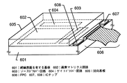
また、対向電極と配向膜とを備えた対向基板を用意し、アクティブマトリクス基板と対向基板との間に液晶材料を封入すれば図6に示す様な構造のアクティブマトリクス型液晶表示装置が完成する。液晶材料を封入する工程は、公知のセル組工程を用いれば良いので詳細な説明は省略する。
【0067】
なお、図6において601は絶縁表面を有する基板、602は画素マトリクス回路、603はソースドライバー回路、604はゲイトドライバー回路、605は対向基板、606はFPC(フレキシブルプリントサーキット)、607及び608は外付けされたICチップである。
【0068】
ICチップ607、608は必要に応じて取り付ければ良く、場合によってはICチップの代わりに同等の機能を有する回路をソースドライバー回路やゲイトドライバー回路などと一体形成してしまっても構わない。即ち、D/Aコンバータやγ補正回路などの信号処理回路をTFTでもって構成しても良い。
【0069】
さらに、本実施例では液晶表示装置を例に挙げて説明しているが、アクティブマトリクス型の表示装置であればEL(エレクトロルミネッセンス)表示装置やEC(エレクトロクロミックス)表示装置に本願発明を適用することも可能であることは言うまでもない。
【0070】
〔実施例2〕
本実施例では図1に示した構造において、絶縁膜107を遮光性を有する樹脂材料(代表的には黒色樹脂材料)とし、その部分をブラックマスクとして活用した。本実施例の構造を図7に示す。なお、本実施例の構成は、実施例1において絶縁膜107の材料を変えただけであり、実施例1と組み合わせることは容易である。
【0071】
図7に示す構造は図1に示す構造と基本的には同一であるが、黒色樹脂材料701で層間絶縁膜が形成されている点で相違する。黒色樹脂材料701としては、黒色顔料、金属(チタン、クロムなど)材料またはカーボン系材料(グラファイトなど)を分散させた樹脂材料を用いることができるが、ブラックマスクとして活用するには、OD値が3以上であることが望ましい。本実施例ではグラファイトを分散させた樹脂材料(OD値が3)を利用した。
【0072】
なお、OD値とは薄膜の遮光性を表す指針であり、OD=−log10 T(Tは透過率で透過率 0.1%の場合はT=0.001 を代入する)で表される。即ち、OD値の絶対値が高いほど透過率が高いことを意味する。
【0073】
この様に、黒色樹脂材料を利用することで、TFT、ソース配線及びゲイト配線を黒色の層間絶縁膜で覆うことが可能となり、そのままブラックマスクとして活用できた。即ち、本実施例の技術を利用すれば工程を簡略化できる。
【0074】
ただし、黒色樹脂材料は層間絶縁膜としても機能するため可能なかぎり高抵抗な材料を選択する必要がある。ところが大抵の黒色樹脂材料は導電性物質を分散させて得るため、抵抗値が低くなってしまうという問題がある。
【0075】
特に、OD値(Optical Density )を上げるために分散物質を多く含ませるので、抵抗値の低さが問題となる。そこで本実施例では、図7に示す様にソース配線702の上方の黒色樹脂材料701に開口部703を形成し、隣接する画素電極間を完全に絶縁分離させた。これにより隣接する画素電極間にクロストークが発生するのを防止できた。
【0076】
この開口部703は画素電極704をマスクとして層間絶縁膜701をエッチングすることで容易に形成できた。エッチングは酸素プラズマによるドライエッチングで行った。この様な構成では、開口部703が遮光性を有するソース配線702の上に位置するため、開口部703から光が差し込んだとしても半導体層(活性層)に到達することはなかった。
【0077】
〔実施例3〕
本実施例では図8に示す様に、層間絶縁膜として透明樹脂材料801と黒色樹脂材料802との積層構造を採用した。なお、本実施例の構成は、実施例1において絶縁膜308を積層構造とする点で異なるだけであり、実施例1と組み合わせることは容易である。
【0078】
本実施例では透明樹脂材料801としてアクリルを用い、黒色樹脂材料802としてチタンを分散させたアクリルを用いた。
【0079】
本実施例ではチタン含有量の多い樹脂材料を用いたため、黒色樹脂材料自体のシート抵抗値は 1×10⁵ Ω/□と低いが、チタン含有量が多い分、より高い遮光性を実現することが可能であった。
【0080】
即ち、遮光性を優先させるには抵抗値の低い黒色樹脂材料を用いる必要があるため、絶縁性を確保するためにシート抵抗値が 1×10¹¹Ω/□程度と高い透明樹脂材料を積層して用いる点に特徴がある。
【0081】
本実施例の構造においても、図7の構造と同様に画素電極をマスクとして黒色樹脂材料802及び透明樹脂材料801を除去して開口部804を形成しておくことが望ましい。この時、透明樹脂材料801のみを残すことも可能である。勿論、開口部804では遮光性が損なわれるので、開口部804がソース配線805上に位置する様に設計しておくことが望ましい。
【0082】
〔実施例4〕
本実施例では、図1に示した構造において補助容量109の下部電極として機能する第1透明導電膜104を、コモン電位(接地電位)に固定するための構造について図9を用いて説明する。
【0083】
図9に示す構造は液晶表示装置の画像表示領域(パネル部分)の外側に設けられた接地用パッドを拡大した図である。第1透明導電膜901と容量用絶縁膜902とは開口部903を有している。この開口部903は、実施例1に示した図3(C)の工程と同時に形成した。
【0084】
本実施例の構造では、開口部903を形成する際に容量用絶縁膜902の端面を第1透明導電膜901の端面よりも後退させて、図9に示す様に階段状の開口部を形成することが重要である。
【0085】
そして、904は樹脂材料からなる層間絶縁膜であり、その上にコモンコンタクト用のパッドとして用いられるパッド電極905を第2透明導電膜でもって形成した。このパッド電極905は実施例1に示した図4(B)の工程と同時に形成した。
【0086】
本実施例の構造では、第1透明導電膜901とパッド電極905とが接触面906で接することによって同電位となる。そして、パッド電極905が接地されることで第1透明導電膜901が接地電位に固定される。
【0087】
また、このコモンコンタクト用パッドは、対向電極を接地電位に固定するためのパッドとして機能させる。パッド電極905上に導電性粒子を混ぜたペースト材料を形成し、その状態でアクティブマトリクス基板と対向基板とを張り合わせることで対向基板に設けられた対向電極とパッド電極との導通をとり、両電極を接地電位に固定することができる。
【0088】
この様に、パッド電極905として画素電極と同一層に形成された透明導電膜を利用すると、大幅に工程を簡略化できるので有効である。
【0089】
なお、本実施例の構造は実施例1〜実施例3の全ての実施例との組み合わせが可能である。
【0090】
〔実施例5〕
本実施例では、TFTのドレイン電極上において平坦化膜を除去する工程を加えた場合の例について図10を用いて説明する。
【0091】
まず、実施例1の工程で従って図3(C)の状態を得た。そして、この図3(C)の状態で酸素プラズマによるドライエッチングを行った。このエッチングによってパターン形成された容量用絶縁膜305をマスクとして、樹脂材料でなる平坦化膜303の一部が除去される。この状態を図10(A)に示す。
【0092】
図10(A)はドライエッチング法によって落とし込み部11を形成した後に、樹脂材料(本実施例ではポリイミド)でなる層間絶縁膜12を形成した状態である。なお、落とし込み部11の開口幅は、図3(C)に示した開口部307の開口幅とほぼ同一である。
【0093】
そして、層間絶縁膜12をパターニングしてパターン化された層間絶縁膜13を形成すると同時に画素電極とTFTとを接続するためのコンタクトホール14を形成した。(図10(B))
【0094】
こうしてコンタクトホール14を形成したら、第2透明導電膜を形成してパターニングを行い、TFTに接続する画素電極15を形成した。また、この時、補助容量16も同時に形成された。
【0095】
本実施例の構造とした場合、コンタクトホール14が同一材料のエッチングのみで形成できる点に利点がある。
【0096】
例えば、実施例1の構造で平坦化膜303としてアクリルを用い、層間絶縁膜308としてポリイミドを用いる組み合わせを採用した場合を想定する。この場合、アクリルの方が若干エッチングレートが速いので、第1透明導電膜304の下にえぐれを生じる可能性があり、画素電極のカバレッジ不良、即ち断線不良を招く危険性があった。
【0097】
その点、本実施例の構造ならばコンタクトホールが完全に同一材料内で形成されるので、エッチングレートの差によるコンタクトホールの形状異常はなく、えぐれなどによる画素電極の断線不良を防止することが可能であった。
【0098】
なお、本実施例の構成は実施例1〜4に示したどの実施例との組み合わせも可能である。どの構成と組み合わせてもコンタクトホールの形状による画素電極の断線不良を防止するという効果は同様である。
【0099】
〔実施例6〕
実施例1〜5の構成を有する本願発明の電気光学装置は、様々な電子機器のディスプレイとして利用される。その様な電子機器としては、ビデオカメラ、スチルカメラ、プロジェクター、プロジェクションTV、ヘッドマウントディスプレイ、カーナビゲーション、パーソナルコンピュータ、携帯情報端末(モバイルコンピュータ、携帯電話等)などが挙げられる。それらの一例を図11に示す。
【0100】
図11(A)は携帯電話であり、本体2001、音声出力部2002、音声入力部2003、表示装置2004、操作スイッチ2005、アンテナ2006で構成される。本願発明を表示装置2004等に適用することができる。
【0101】
図11(B)はビデオカメラであり、本体2101、表示装置2102、音声入力部2103、操作スイッチ2104、バッテリー2105、受像部2106で構成される。本願発明を表示装置2102に適用することができる。
【0102】
図11(C)はモバイルコンピュータ(モービルコンピュータ)であり、本体2201、カメラ部2202、受像部2203、操作スイッチ2204、表示装置2205で構成される。本願発明は表示装置2205等に適用できる。
【0103】
図11(D)はヘッドマウントディスプレイであり、本体2301、表示装置2302、バンド部2303で構成される。本発明は表示装置2302に適用することができる。
【0104】
図11(E)はリア型プロジェクターであり、本体2401、光源2402、表示装置2403、偏光ビームスプリッタ2404、リフレクター2405、2406、スクリーン2407で構成される。本発明は表示装置2403に適用することができる。
【0105】
図11(F)はフロント型プロジェクターであり、本体2501、光源2502、表示装置2503、光学系2504、スクリーン2505で構成される。本発明は表示装置2503に適用することができる。
【0106】
以上の様に、本願発明の適用範囲は極めて広く、あらゆる分野の電子機器に適用することが可能である。
【0107】
【発明の効果】
本願発明を実施することで、透明導電膜で挟持された容量用絶縁膜の膜厚を自由に設定できる様になったため、画素内の光透過率を損ねることなく、画素全域を補助容量として利用することが可能となった。
【0108】
そのため、画素面積の小さい高精細なアクティブマトリクス型表示装置を形成する場合に、十分な補助容量を確保することが可能となった。また、画素内全域を補助容量としても光透過率が十分に高いので、明るい画像表示が可能であった。即ち、高精細で高品質の電気光学装置及びその様な電気光学装置を搭載した電子機器を実現することができた。
【図面の簡単な説明】
【図1】 画素及び補助容量の断面構造を示す図。
【図2】 従来の画素及び補助容量の断面構造を示す図。
【図3】 画素構造の作製工程を示す図。
【図4】 画素構造の作製工程を示す図。
【図5】 画素構造の上面図を示す図。
【図6】 アクティブマトリクス型液晶表示装置の外観を示す図。
【図7】 画素及び補助容量の断面構造を示す図。
【図8】 画素及び補助容量の断面構造を示す図。
【図9】 コモンコンタクト部の断面構造を示す図。
【図10】 画素構造の作製工程を示す図。
【図11】 電子機器の一例を示す図。[0001]
[Technical field to which the invention belongs]
The present invention relates to an electro-optical device typified by a liquid crystal display device and a configuration of an electronic apparatus in which such an electro-optical device is mounted as a component. Note that in this specification, a semiconductor device refers to all devices that can function by utilizing semiconductor characteristics, and includes the above electro-optical devices and electronic devices in the category of semiconductor devices.
[0002]
[Prior art]
In recent years, attention has been paid to an active matrix liquid crystal display device in which a circuit is constituted by a thin film transistor (hereinafter referred to as TFT) using a polysilicon film. This realizes high-definition image display by controlling the electric field applied to the liquid crystal in a matrix by a plurality of pixels arranged in a matrix.
[0003]
In such an active matrix type liquid crystal display device, a capacitor (capacitor) is formed by the pixel electrode formed for each pixel and the counter electrode formed on the opposite side via the liquid crystal. Since it is small, it is usually supplemented by forming an auxiliary capacitor (also called Cs) separately from it.
[0004]
There are various auxiliary capacitor structures (Cs structures), but a structure in which an insulating film is sandwiched between two transparent conductive films in consideration of the aperture ratio in a transmissive liquid crystal display device has been reported (Japanese Patent Laid-Open No. 8-43854). No., JP-A-8-306926).
[0005]
According to the Cs structure described in the above publication, a large capacity can be secured without impairing the aperture ratio by using both of the two sets of electrodes constituting the auxiliary capacity as transparent conductive films such as ITO.
[0006]
In the above publication, the interlayer insulating film also serves as a dielectric for the auxiliary capacitor. However, a certain degree of film thickness is required to fulfill the function as the interlayer insulating film. That is, as shown in FIG. 2, since the interlayer insulating film 202 is formed so as to cover the capacitive electrode 201 made of a transparent conductive film, a film thickness that does not cause a coverage defect in the end portion 203 must be guaranteed at a minimum.
[0007]
In addition, since the transparent conductive film has a higher resistance than the metal film, the thickness of the capacitor electrode 201 needs to be about 100 to 200 nm even in consideration of the potential distribution. Therefore, in order to completely cover the capacitor electrode 201, an insulating film having a thickness of at least 200 nm is required. However, since the capacity is inversely proportional to the film thickness of the dielectric, increasing the film thickness is not desirable for securing a large capacity.
[0008]
As described above, it is possible to expand the area where the auxiliary capacitance can be formed without impairing the aperture ratio by sandwiching two sets of transparent conductive films between insulating films, but there are still many problems. This is the current situation.
[0009]
[Problems to be solved by the invention]
The present invention is a technique for solving the above-described problems, and an object thereof is to further improve an electro-optical device having an auxiliary capacity using two sets of transparent conductive films. Another object is to provide a higher quality semiconductor device.
[0010]
[Means for Solving the Problems]
The configuration of the invention disclosed in this specification is as follows.
In a semiconductor device having a plurality of pixels arranged in a matrix and an auxiliary capacitor provided in each of the plurality of pixels,
The auxiliary capacitor has a structure in which a first transparent conductive film, a capacitor insulating film, and a second transparent conductive film are sequentially stacked,
The first transparent conductive film and the capacitor insulating film have the same pattern shape.
[0011]
The first transparent conductive film and the capacitor insulating film can be sequentially etched with the same mask when an etchant (or etching gas) that can etch both films is used. In that case, the first transparent conductive film and the capacitor insulating film have openings of the same shape. The opening is covered with a resin material patterned by patterning.
[0012]
At this time, the resin material can be formed of a light-blocking resin material (black resin material or the like) or a laminated structure of a light-blocking resin material and a transparent resin material (acrylic, polyimide, or the like).
[0013]
In addition, the configuration of other inventions is as follows:
Forming a first transparent conductive film and a capacitor insulating film on the first interlayer insulating film covering the TFT;
Etching the first transparent conductive film and the capacitor insulating film to form an opening having the same shape in each of the first transparent conductive film and the capacitor insulating film;
Forming a second interlayer insulating film made of a resin material so as to cover the opening;
Removing the second interlayer insulating film formed in the opening and the portion that later becomes an auxiliary capacitor;
Etching the first interlayer insulating film exposed at the opening to form a contact hole;
Forming a second transparent conductive film connected to the TFT;
Patterning the second transparent conductive film to form pixel electrodes;
Have
The auxiliary capacitor is formed by the first transparent conductive film, the capacitor insulating film, and the pixel electrode.
[0014]
In the above configuration, the first transparent conductive film and the capacitor insulating film are sequentially etched, and the opening provided in the capacitor insulating film has a larger aperture than the opening provided in the first transparent conductive film. By having such a structure, a stepped opening can be formed.
[0015]
DETAILED DESCRIPTION OF THE INVENTION
An embodiment of a liquid crystal display device using the present invention will be described with reference to FIG. FIG. 1 is a cross-sectional view showing a plurality of pixels arranged in a matrix and auxiliary capacitors provided in each pixel.
[0016]
In FIG. 1, reference numeral 101 denotes a substrate having an insulating surface, on which a TFT 102 formed by a known means is formed. A planarizing film (first interlayer insulating film) 103 was formed so as to cover the TFT 102. Although any insulating film can be used for the planarizing film 103, it is preferable to use a resin material such as polyimide or acrylic in order to achieve high planarity.
[0017]
A first transparent conductive film 104 and a capacitor insulating film 105 were sequentially stacked on the planarizing film 103. As the first transparent conductive film 104, tin oxide, ITO (indium tin oxide), or the like may be used. The first transparent conductive film 104 functions as a lower electrode of the auxiliary capacitor.
[0018]
As the capacitor insulating film 105, a transparent insulating film such as silicon oxide, silicon nitride, silicon oxynitride, tantalum oxide, or aluminum oxide (alumina) was used. The capacitor insulating film 105 functions as an auxiliary capacitor dielectric and is formed over the entire area of the pixel, so that an insulating film with high transmittance is preferable.
[0019]
In the invention of the present application, a large area of the auxiliary capacitor can be secured and the dielectric film thickness can be reduced (described later), so that an insulating film having a relatively high relative dielectric constant is not required. Therefore, since it is possible to select an optimum insulating film with the highest priority on increasing the transmittance, a bright image display is possible.
[0020]
An opening 106 was formed in the laminated structure including the first transparent conductive film 104 and the capacitor insulating film 105. This is a connection portion (hereinafter referred to as a drain connection portion) for connecting the pixel electrode and the drain electrode later.
[0021]
At this time, if dry etching is performed using an etching gas capable of etching both the first transparent conductive film 104 and the capacitor insulating film 105, the first transparent exposed at the opening 106 as shown in FIG. The end face of the conductive film and the end face of the capacitor insulating film are almost aligned. The same applies to wet etching using an etchant that can etch both.
[0022]
Further, if the capacitor insulating film 105 is etched under conditions such that the etching rate is faster, the opening provided in the capacitor insulating film has a larger diameter than the opening provided in the first transparent conductive film. And the stepped opening can be formed.
[0023]
Then, an insulating film 107 having a low relative dielectric constant was formed so as to cover the opening 106, and the insulating film 107 was patterned. In the patterning step, only the portion where the auxiliary capacitance is formed and the insulating film 107 formed in the drain connection portion are selectively removed, a contact hole is formed in the drain connection portion (opening portion 106), and the capacitance insulating film 105 is formed. It was in an exposed state.
[0024]
A pixel electrode 108 made of a second transparent conductive film was formed thereon. The pixel electrode 108 was in contact with the capacitor insulating film 105 in the pixel, and an auxiliary capacitor 109 composed of the first transparent conductive film / capacitor insulating film / second transparent conductive film could be formed.
[0025]
The pixel electrode 108 is electrically connected to the drain electrode 110 of the TFT 102, and the voltage applied to the pixel electrode 108 is controlled by the TFT 102. Although FIG. 1 shows a structure in which the pixel electrode 108 is connected to the drain electrode 110, a structure in which the pixel electrode 108 is directly connected to the active layer of the TFT 102 may be used.
[0026]
In the structure shown in FIG. 1, the TFT 102 is completely shielded by a black mask provided on the counter substrate side of the liquid crystal display device. This is to prevent the active layer of the TFT 102 from being irradiated with light.
[0027]
A feature of the present invention having the above-described configuration is that the film thickness of the capacitor insulating film 105 (dielectric of auxiliary capacitor) can be freely adjusted. In the structure described in the conventional example, a film thickness of 200 nm or more is required due to the problem of coverage, but in the structure of the present invention, it was possible to form the film with a thickness of about 10 to 200 nm (preferably 50 to 100 nm). . That is, the thickness of the capacitor insulating film 105 can be made thinner than that of the first transparent conductive film 104.
[0028]
The reason why the lower limit of the film thickness is set to 10 nm is that if it is less than this, the breakdown voltage is weak and dielectric breakdown tends to occur. Another reason is that below this, it is difficult to ensure a uniform film thickness. In view of such reasons, it can be said that a film thickness of about 50 to 100 nm is preferable.
[0029]
Basically, there is no upper limit to the thickness of the capacitor insulating film 105. However, if the thickness is too large, it is difficult to secure a large capacity and the throughput is lowered. In this sense, the applicant considers the upper limit to be 200 nm (preferably 100 nm).
[0030]
Thus, the fact that the film thickness of the dielectric of the auxiliary capacitor can be set freely is a very great advantage. As is generally known, there is a condition (antireflection condition) that increases the transmittance when thin films having different refractive indexes are laminated. This relationship is given by nd = λ / 4 where n is the refractive index, d is the film thickness, and λ is the transmitted light wavelength.
[0031]
In the present invention, since the selection range of the dielectric material and the film thickness of the auxiliary capacitor is wide, it is easy to adjust the term nd in the above formula. Therefore, by controlling the film thickness of each laminated film so as to match the antireflection condition, a high transmittance can be realized, and a pixel region capable of displaying a bright image while functioning as an auxiliary capacitor can be formed.
[0032]
In the case of the configuration of the present invention, since the insulating film 107 is disposed between the pixel electrode 108 and the first transparent conductive film 104 in the opening 106, the end surfaces of the pixel electrode 108 and the first transparent conductive film 104 are used. And are not short-circuited.
[0033]
The present invention configured as described above will be described in more detail with reference to the following examples.
[0034]
【Example】
[Example 1]
A manufacturing process example in the case of manufacturing a liquid crystal display device as a semiconductor device having the structure of the present invention will be described with reference to FIGS.
[0035]
First, a glass substrate provided with a base film made of silicon oxide on the surface was prepared as a substrate having an insulating surface. Of course, in addition to the glass substrate, a quartz substrate (there may be no base) or a ceramic glass substrate may be used, or a silicon wafer on which a thermal oxide film is formed may be used.
[0036]
Next, the TFT 102 was completed by a known means. In this embodiment, the technique described in Japanese Patent Application Laid-Open No. 7-135318 by the applicant is used. According to the technique described in the publication, a
[0037]
Next, a
[0038]
As the first transparent
[0039]
When a resin material is used as the base (planarizing film) as in this embodiment, a process that requires heating the substrate is inappropriate because degassing from the resin material becomes a problem. In that respect, the sputtering method is a suitable means because it allows film formation at room temperature.
[0040]
As the
[0041]
In this embodiment, the target is SiO. 2 Using a mixed gas of argon (30 sccm) and oxygen (10 sccm) as the sputtering gas, the deposition pressure is 3 × 10 -3 set to torr. In addition, the film formation was performed under RF power control of 2000 W, and the substrate temperature was room temperature.
[0042]
In this case, since the first transparent
[0043]
According to the knowledge of the present applicant, when the substrate temperature of the
[0044]
Experimental results have shown that it is necessary to form a film in a temperature range of preferably 180 ° C. or lower (preferably 100 to 150 ° C.), and for that purpose, sputtering is the most preferable film forming method. It can be said.
[0045]
Of course, if the film can be formed in the temperature range as described above, it can be formed by the CVD method. Further, when the first transparent
[0046]
Although a silicon oxide film is used as the
[0047]
When the state of FIG. 3B is thus obtained, an
[0048]
In this embodiment, the
[0049]
In the formation of the
[0050]
In this embodiment, buffered hydrofluoric acid was used for etching the capacitor insulating film 305 (silicon oxide film) and the first transparent conductive film (ITO film) 304. Since the silicon oxide film and the ITO film have substantially the same etching rate with respect to buffered hydrofluoric acid, the openings provided in both of them can have the same shape.
[0051]
At this time, if the capacitor insulating film has a higher etching rate, a stepped opening can be formed, and an opening with good coverage can be formed. Such conditions can be adjusted by the type of etchant, the insulating film for capacitance, the film quality of the first transparent conductive film, and the like. Of course, the patterning may be performed twice and the etching process may be performed separately.
[0052]
Next, an interlayer insulating film (second interlayer insulating film) 308 having a low relative dielectric constant was formed to cover the
[0053]
After the
[0054]
In this state, since the
[0055]
At the same time, a
[0056]
In this step, first, a resist mask (not shown) was formed at a predetermined position of the
[0057]
Then, an ITO film having a thickness of 120 nm was formed as the second transparent conductive film, and the
[0058]
A top view of the pixel in a state where the
[0059]
In FIG. 5, 501 is an active layer made of a semiconductor thin film, 502 is a gate wiring, and a portion where the
[0060]
[0061]
The pixel structure of the present embodiment configured as described above has an advantage that the area serving as the auxiliary capacitance occupies almost the entire area of the pixel, and the area substantially the same as the image display area can be secured.
[0062]
In particular, the characteristic of the structure of this example is that the first transparent conductive film and the capacitor insulating film are stacked, so that the thickness of the capacitor insulating film is 10 to 200 nm (preferably 50 to 100 nm).
[0063]
Therefore, since the proportion of the capacitance forming area is large and an auxiliary capacitance with a thin dielectric film thickness can be formed, a sufficient capacitance can be secured even if the relative dielectric constant is not so high. This means that the degree of freedom of materials that can be selected is greatly expanded.
[0064]
As a result, it is possible to select materials with priority on high transmittance characteristics, and to achieve high transmittance with an antireflection effect by appropriately combining the film thickness of transparent conductive film and capacitive insulating film Is also possible. In that respect, in the conventional structure, since the dielectric material and film thickness are limited to some extent, such a degree of freedom is small.
[0065]
Note that the state shown in FIG. 4B is a state in which the TFT formation side substrate (active matrix substrate) of the liquid crystal display device is almost completed. Actually, there is a step of forming an alignment film so as to cover the pixel electrode.
[0066]
Further, if an opposing substrate having an opposing electrode and an alignment film is prepared and a liquid crystal material is sealed between the active matrix substrate and the opposing substrate, an active matrix type liquid crystal display device having a structure as shown in FIG. 6 is completed. . Since the process of encapsulating the liquid crystal material may use a known cell assembly process, detailed description thereof is omitted.
[0067]
In FIG. 6, 601 is a substrate having an insulating surface, 602 is a pixel matrix circuit, 603 is a source driver circuit, 604 is a gate driver circuit, 605 is a counter substrate, 606 is an FPC (flexible printed circuit), and 607 and 608 are outside. IC chip attached.
[0068]
The IC chips 607 and 608 may be attached as necessary. In some cases, a circuit having an equivalent function may be integrally formed with a source driver circuit, a gate driver circuit, or the like instead of the IC chip. That is, a signal processing circuit such as a D / A converter or a γ correction circuit may be configured with a TFT.
[0069]
Further, in this embodiment, the liquid crystal display device is described as an example, but the present invention is applied to an EL (electroluminescence) display device and an EC (electrochromic) display device as long as it is an active matrix display device. It goes without saying that it is also possible to do.
[0070]
[Example 2]
In this embodiment, in the structure shown in FIG. 1, the insulating film 107 is made of a light shielding resin material (typically a black resin material), and this portion is used as a black mask. The structure of this example is shown in FIG. Note that the configuration of this example is merely that the material of the insulating film 107 is changed in Example 1, and can be easily combined with Example 1.
[0071]
The structure shown in FIG. 7 is basically the same as the structure shown in FIG. 1 except that an interlayer insulating film is formed of a black resin material 701. As the black resin material 701, a black pigment, a metal material (such as titanium or chromium), or a resin material in which a carbon-based material (such as graphite) is dispersed can be used. It is desirable to be 3 or more. In this embodiment, a resin material (OD value is 3) in which graphite is dispersed is used.
[0072]
The OD value is a guideline indicating the light-shielding property of the thin film, and OD = −log Ten T (T is transmittance and T = 0.001 is substituted when the transmittance is 0.1%). That is, the higher the absolute value of the OD value, the higher the transmittance.
[0073]
Thus, by using the black resin material, the TFT, the source wiring and the gate wiring can be covered with the black interlayer insulating film, and can be used as it is as a black mask. That is, the process can be simplified by using the technique of this embodiment.
[0074]
However, since the black resin material also functions as an interlayer insulating film, it is necessary to select a material having the highest possible resistance. However, most black resin materials are obtained by dispersing a conductive substance, which causes a problem that the resistance value is lowered.
[0075]
In particular, since a large amount of dispersed material is included to increase the OD value (Optical Density), the low resistance value becomes a problem. Therefore, in this embodiment, as shown in FIG. 7, the opening 703 is formed in the black resin material 701 above the source wiring 702, and the adjacent pixel electrodes are completely insulated and separated. As a result, it was possible to prevent crosstalk from occurring between adjacent pixel electrodes.
[0076]
The opening 703 can be easily formed by etching the interlayer insulating film 701 using the pixel electrode 704 as a mask. Etching was performed by dry etching using oxygen plasma. In such a configuration, since the opening 703 is positioned on the light-shielding source wiring 702, even if light is inserted from the opening 703, the semiconductor layer (active layer) is not reached.
[0077]
Example 3
In this embodiment, as shown in FIG. 8, a laminated structure of a transparent resin material 801 and a black resin material 802 is adopted as an interlayer insulating film. Note that the configuration of this example differs only in that the insulating
[0078]
In this embodiment, acrylic was used as the transparent resin material 801, and acrylic in which titanium was dispersed was used as the black resin material 802.
[0079]
In this example, since a resin material with a high titanium content was used, the sheet resistance value of the black resin material itself was 1 × 10 Five Although it was as low as Ω / □, the higher the titanium content, the higher the light-shielding property could be realized.
[0080]
That is, in order to prioritize light shielding, it is necessary to use a black resin material having a low resistance value. Therefore, in order to ensure insulation, the sheet resistance value is 1 × 10. 11 It is characterized in that a transparent resin material having a high resistance of about Ω / □ is used.
[0081]
Also in the structure of this embodiment, it is desirable to form the opening 804 by removing the black resin material 802 and the transparent resin material 801 using the pixel electrode as a mask as in the structure of FIG. At this time, it is possible to leave only the transparent resin material 801. Needless to say, since the light shielding property is impaired in the opening 804, it is desirable to design the opening 804 so as to be positioned on the source wiring 805.
[0082]
Example 4
In this embodiment, a structure for fixing the first transparent conductive film 104 functioning as the lower electrode of the auxiliary capacitor 109 to the common potential (ground potential) in the structure shown in FIG. 1 will be described with reference to FIG.
[0083]
The structure shown in FIG. 9 is an enlarged view of a grounding pad provided outside the image display area (panel portion) of the liquid crystal display device. The first transparent conductive film 901 and the capacitor insulating film 902 have an opening 903. This opening 903 was formed at the same time as the step of FIG.
[0084]
In the structure of this embodiment, when the opening 903 is formed, the end face of the capacitor insulating film 902 is made to recede from the end face of the first transparent conductive film 901 to form a stepped opening as shown in FIG. It is important to.
[0085]
Reference numeral 904 denotes an interlayer insulating film made of a resin material, and a pad electrode 905 used as a common contact pad is formed thereon with a second transparent conductive film. The pad electrode 905 was formed at the same time as the step of FIG.
[0086]
In the structure of the present embodiment, the first transparent conductive film 901 and the pad electrode 905 are brought into contact with each other at the contact surface 906 to have the same potential. Then, the first transparent conductive film 901 is fixed to the ground potential by the pad electrode 905 being grounded.
[0087]
The common contact pad functions as a pad for fixing the counter electrode to the ground potential. A paste material mixed with conductive particles is formed on the pad electrode 905, and in this state, the active matrix substrate and the counter substrate are bonded to establish conduction between the counter electrode provided on the counter substrate and the pad electrode. The electrode can be fixed at ground potential.
[0088]
In this manner, using a transparent conductive film formed in the same layer as the pixel electrode as the pad electrode 905 is effective because the process can be greatly simplified.
[0089]
Note that the structure of this embodiment can be combined with all of the
[0090]
Example 5
In this embodiment, an example in which a step of removing the planarizing film on the drain electrode of the TFT is added will be described with reference to FIG.
[0091]
First, in the process of Example 1, the state shown in FIG. Then, dry etching using oxygen plasma was performed in the state of FIG. A part of the
[0092]
FIG. 10A shows a state in which an interlayer insulating film 12 made of a resin material (polyimide in this embodiment) is formed after forming the drop portion 11 by dry etching. Note that the opening width of the dropping portion 11 is substantially the same as the opening width of the
[0093]
Then, the interlayer insulating film 12 was patterned to form a patterned interlayer insulating film 13, and at the same time, a contact hole 14 for connecting the pixel electrode and the TFT was formed. (Fig. 10 (B))
[0094]
After the contact hole 14 was formed in this way, a second transparent conductive film was formed and patterned to form a pixel electrode 15 connected to the TFT. At this time, the auxiliary capacitor 16 was also formed at the same time.
[0095]
The structure of this embodiment is advantageous in that the contact hole 14 can be formed only by etching the same material.
[0096]
For example, it is assumed that the structure of the first embodiment uses a combination of acrylic as the
[0097]
In that respect, since the contact hole is formed entirely in the same material in the structure of this embodiment, there is no abnormality in the shape of the contact hole due to the difference in the etching rate, and it is possible to prevent the disconnection failure of the pixel electrode due to erosion or the like. It was possible.
[0098]
In addition, the structure of a present Example can be combined with any Example shown in Examples 1-4. Regardless of the configuration, the effect of preventing disconnection failure of the pixel electrode due to the shape of the contact hole is the same.
[0099]
Example 6
The electro-optical device of the present invention having the configurations of Examples 1 to 5 is used as a display of various electronic devices. Examples of such an electronic device include a video camera, a still camera, a projector, a projection TV, a head mounted display, a car navigation, a personal computer, a portable information terminal (mobile computer, mobile phone, etc.), and the like. An example of them is shown in FIG.
[0100]
FIG. 11A illustrates a mobile phone, which includes a main body 2001, an audio output unit 2002, an audio input unit 2003, a display device 2004, operation switches 2005, and an antenna 2006. The present invention can be applied to the display device 2004 and the like.
[0101]
FIG. 11B illustrates a video camera, which includes a main body 2101, a display device 2102, an
[0102]
FIG. 11C illustrates a mobile computer, which includes a main body 2201, a camera unit 2202, an
[0103]
FIG. 11D illustrates a head mounted display which includes a
[0104]
FIG. 11E shows a rear projector, which includes a main body 2401, a light source 2402, a display device 2403, a
[0105]
FIG. 11F illustrates a front projector, which includes a
[0106]
As described above, the application range of the present invention is extremely wide and can be applied to electronic devices in various fields.
[0107]
【The invention's effect】
By implementing the present invention, the film thickness of the capacitor insulating film sandwiched between the transparent conductive films can be freely set, so that the entire pixel area can be used as an auxiliary capacitor without impairing the light transmittance in the pixel. It became possible to do.
[0108]
Therefore, when forming a high-definition active matrix display device with a small pixel area, it is possible to secure a sufficient auxiliary capacity. Moreover, since the light transmittance is sufficiently high even when the entire area in the pixel is used as an auxiliary capacitor, a bright image display is possible. That is, a high-definition and high-quality electro-optical device and an electronic apparatus equipped with such an electro-optical device can be realized.
[Brief description of the drawings]
FIG. 1 is a diagram showing a cross-sectional structure of a pixel and an auxiliary capacitor.
FIG. 2 is a diagram showing a cross-sectional structure of a conventional pixel and auxiliary capacitor.
FIGS. 3A and 3B are diagrams illustrating a manufacturing process of a pixel structure. FIGS.
FIGS. 4A and 4B are diagrams illustrating a manufacturing process of a pixel structure. FIGS.
FIG. 5 is a top view of a pixel structure.
FIG. 6 is a diagram showing the appearance of an active matrix liquid crystal display device.
FIG. 7 illustrates a cross-sectional structure of a pixel and an auxiliary capacitor.
FIG. 8 illustrates a cross-sectional structure of a pixel and an auxiliary capacitor.
FIG. 9 is a diagram showing a cross-sectional structure of a common contact portion.
FIGS. 10A and 10B are diagrams illustrating a manufacturing process of a pixel structure. FIGS.
FIG 11 illustrates an example of an electronic device.
Claims (6)
前記第1透明導電膜上に容量用絶縁膜を形成し、
前記第1透明導電膜及び前記容量用絶縁膜をエッチングして、当該第1透明導電膜及び当該容量用絶縁膜を貫通する開口部を形成し、
前記開口部を覆うように樹脂材料を形成し、
前記容量用絶縁膜の上面の一部を露出するように前記樹脂材料をパターニングして第2層間絶縁膜を形成し、
前記開口部において、前記第2層間絶縁膜と前記第1層間絶縁膜とをエッチングしてコンタクトホールを形成し、
前記コンタクトホールにおいて、前記薄膜トランジスタと接続する第2透明導電膜を形成し、
前記第2透明導電膜をパターニングして、前記容量用絶縁膜を間に挟んで前記第1透明導電膜と重なる画素電極を形成することを特徴とする半導体装置の作製方法。Forming a first transparent conductive film on the first interlayer insulating film covering the thin film transistor;
Forming a capacitor insulating film on the first transparent conductive film;
Etching the first transparent conductive film and the capacitor insulating film to form an opening that penetrates the first transparent conductive film and the capacitor insulating film;
Forming a resin material so as to cover the opening,
Patterning the resin material to expose a part of the upper surface of the capacitor insulating film to form a second interlayer insulating film;
In the opening, the second interlayer insulating film and the first interlayer insulating film are etched to form a contact hole,
Forming a second transparent conductive film connected to the thin film transistor in the contact hole;
A method of manufacturing a semiconductor device, comprising patterning the second transparent conductive film to form a pixel electrode overlapping the first transparent conductive film with the capacitor insulating film interposed therebetween.
前記第1透明導電膜上に容量用絶縁膜を形成し、
前記第1透明導電膜及び前記容量用絶縁膜を順次エッチングして、当該第1透明導電膜及び当該容量用絶縁膜を貫通する階段状の開口部を形成し、
前記開口部を覆うように樹脂材料を形成し、
前記容量用絶縁膜の上面の一部を露出するように前記樹脂材料をパターニングして第2層間絶縁膜を形成し、
前記開口部において、前記第2層間絶縁膜と前記第1層間絶縁膜とをエッチングしてコンタクトホールを形成し、
前記コンタクトホールにおいて、前記薄膜トランジスタと接続する第2透明導電膜を形成し、
前記第2透明導電膜をパターニングして、前記容量用絶縁膜を間に挟んで前記第1透明導電膜と重なる画素電極を形成することを特徴とする半導体装置の作製方法。Forming a first transparent conductive film on the first interlayer insulating film covering the thin film transistor;
Forming a capacitor insulating film on the first transparent conductive film;
The first transparent conductive film and the capacitor insulating film are sequentially etched to form a stepped opening that penetrates the first transparent conductive film and the capacitor insulating film,
Forming a resin material so as to cover the opening,
Patterning the resin material to expose a part of the upper surface of the capacitor insulating film to form a second interlayer insulating film;
In the opening, the second interlayer insulating film and the first interlayer insulating film are etched to form a contact hole,
Forming a second transparent conductive film connected to the thin film transistor in the contact hole;
A method of manufacturing a semiconductor device, comprising patterning the second transparent conductive film to form a pixel electrode overlapping the first transparent conductive film with the capacitor insulating film interposed therebetween.
Priority Applications (2)
| Application Number | Priority Date | Filing Date | Title |
|---|---|---|---|
| JP11905598A JP3941901B2 (en) | 1998-04-28 | 1998-04-28 | Method for manufacturing semiconductor device |
| US09/294,335 US6690031B1 (en) | 1998-04-28 | 1999-04-20 | Semiconductor device and method of manufacturing the same |
Applications Claiming Priority (1)
| Application Number | Priority Date | Filing Date | Title |
|---|---|---|---|
| JP11905598A JP3941901B2 (en) | 1998-04-28 | 1998-04-28 | Method for manufacturing semiconductor device |
Publications (2)
| Publication Number | Publication Date |
|---|---|
| JPH11311805A JPH11311805A (en) | 1999-11-09 |
| JP3941901B2 true JP3941901B2 (en) | 2007-07-11 |
Family
ID=14751800
Family Applications (1)
| Application Number | Title | Priority Date | Filing Date |
|---|---|---|---|
| JP11905598A Expired - Fee Related JP3941901B2 (en) | 1998-04-28 | 1998-04-28 | Method for manufacturing semiconductor device |
Country Status (2)
| Country | Link |
|---|---|
| US (1) | US6690031B1 (en) |
| JP (1) | JP3941901B2 (en) |
Cited By (1)
| Publication number | Priority date | Publication date | Assignee | Title |
|---|---|---|---|---|
| US10068926B2 (en) | 2011-05-05 | 2018-09-04 | Semiconductor Energy Laboratory Co., Ltd. | Semiconductor device and method for manufacturing the same |
Families Citing this family (30)
| Publication number | Priority date | Publication date | Assignee | Title |
|---|---|---|---|---|
| EP0499979A3 (en) | 1991-02-16 | 1993-06-09 | Semiconductor Energy Laboratory Co., Ltd. | Electro-optical device |
| EP1031873A3 (en) * | 1999-02-23 | 2005-02-23 | Sel Semiconductor Energy Laboratory Co., Ltd. | Semiconductor device and fabrication method thereof |
| US6475836B1 (en) * | 1999-03-29 | 2002-11-05 | Semiconductor Energy Laboratory Co., Ltd. | Semiconductor device and manufacturing method thereof |
| JP3796070B2 (en) * | 1999-07-21 | 2006-07-12 | シャープ株式会社 | Liquid crystal display |
| US7023021B2 (en) | 2000-02-22 | 2006-04-04 | Semiconductor Energy Laboratory Co., Ltd. | Semiconductor device and method of manufacturing the same |
| JP4099324B2 (en) | 2000-11-27 | 2008-06-11 | シャープ株式会社 | Liquid crystal display |
| JP4798907B2 (en) | 2001-09-26 | 2011-10-19 | 株式会社半導体エネルギー研究所 | Semiconductor device |
| JP3989761B2 (en) | 2002-04-09 | 2007-10-10 | 株式会社半導体エネルギー研究所 | Semiconductor display device |
| US7038239B2 (en) * | 2002-04-09 | 2006-05-02 | Semiconductor Energy Laboratory Co., Ltd. | Semiconductor element and display device using the same |
| JP3989763B2 (en) | 2002-04-15 | 2007-10-10 | 株式会社半導体エネルギー研究所 | Semiconductor display device |
| US7411215B2 (en) * | 2002-04-15 | 2008-08-12 | Semiconductor Energy Laboratory Co., Ltd. | Display device and method of fabricating the same |
| US7256421B2 (en) | 2002-05-17 | 2007-08-14 | Semiconductor Energy Laboratory, Co., Ltd. | Display device having a structure for preventing the deterioration of a light emitting device |
| TW583464B (en) * | 2002-11-12 | 2004-04-11 | Hannstar Display Corp | Liquid crystal display |
| TWI226712B (en) * | 2003-12-05 | 2005-01-11 | Au Optronics Corp | Pixel structure and fabricating method thereof |
| JP2006126255A (en) * | 2004-10-26 | 2006-05-18 | Mitsubishi Electric Corp | Electrooptical device, liquid crystal display device, and method for manufacturing them |
| KR101112549B1 (en) * | 2005-01-31 | 2012-06-12 | 삼성전자주식회사 | Thin film transistor array panel |
| TWI411095B (en) | 2005-09-29 | 2013-10-01 | Semiconductor Energy Lab | Memory device |
| TWI337754B (en) * | 2007-04-20 | 2011-02-21 | Au Optronics Corp | Semiconductor structure of display device and method for fabricating the same |
| JP5195455B2 (en) * | 2009-01-23 | 2013-05-08 | セイコーエプソン株式会社 | ELECTRO-OPTICAL DEVICE, MANUFACTURING METHOD THEREOF, AND ELECTRONIC DEVICE |
| TWI403413B (en) * | 2009-04-27 | 2013-08-01 | Univ Tatung | Hydrophilic-hydrophobic transformable composite film and the method of fabricating the same |
| US8866982B2 (en) * | 2009-08-20 | 2014-10-21 | Innolux Corporation | Display device |
| US20130010246A1 (en) * | 2010-04-16 | 2013-01-10 | Masahiko Miwa | Method for manufacturing electronic substrate, method for manufacturing liquid crystal display device, electronic substrate, and liquid crystal display device |
| US9230994B2 (en) | 2010-09-15 | 2016-01-05 | Semiconductor Energy Laboratory Co., Ltd. | Liquid crystal display device |
| GB2489939A (en) * | 2011-04-11 | 2012-10-17 | Plastic Logic Ltd | Control of capacitive coupling in pixel circuitry |
| JP5153921B2 (en) * | 2011-06-27 | 2013-02-27 | 株式会社半導体エネルギー研究所 | Display device and portable information terminal |
| JP2013200574A (en) * | 2013-06-05 | 2013-10-03 | Semiconductor Energy Lab Co Ltd | Semiconductor device |
| JP5685633B2 (en) * | 2013-10-08 | 2015-03-18 | 株式会社半導体エネルギー研究所 | Display device |
| CN106502011A (en) * | 2016-12-30 | 2017-03-15 | 深圳市华星光电技术有限公司 | Image element structure and method of work, array base palte |
| CN107065357A (en) * | 2017-05-18 | 2017-08-18 | 深圳市华星光电技术有限公司 | Array base palte and its manufacture method, liquid crystal display panel |
| US10459300B2 (en) | 2017-05-18 | 2019-10-29 | Shenzhen China Star Optoelectronics Semiconductor Display Technology Co., Ltd | Array substrate and a method for fabricating the same, a liquid crystal display panel |
Family Cites Families (31)
| Publication number | Priority date | Publication date | Assignee | Title |
|---|---|---|---|---|
| JPS5617381A (en) | 1979-07-20 | 1981-02-19 | Matsushita Electric Ind Co Ltd | Image display unit |
| JPS58159518A (en) | 1982-03-18 | 1983-09-21 | Seiko Epson Corp | Liquid crystal display panel |
| JPS6045219A (en) * | 1983-08-23 | 1985-03-11 | Toshiba Corp | Active matrix type display device |
| US4639087A (en) * | 1984-08-08 | 1987-01-27 | Energy Conversion Devices, Inc. | Displays having pixels with two portions and capacitors |
| US4728175A (en) * | 1986-10-09 | 1988-03-01 | Ovonic Imaging Systems, Inc. | Liquid crystal display having pixels with auxiliary capacitance |
| JP2602255B2 (en) | 1987-11-27 | 1997-04-23 | 株式会社日立製作所 | Liquid crystal display device and driving method thereof |
| JP2851305B2 (en) | 1989-06-07 | 1999-01-27 | 株式会社日立製作所 | Liquid crystal display |
| JP2604867B2 (en) * | 1990-01-11 | 1997-04-30 | 松下電器産業株式会社 | Reflective liquid crystal display device |
| JP2622183B2 (en) * | 1990-04-05 | 1997-06-18 | シャープ株式会社 | Active matrix display device |
| US5056895A (en) * | 1990-05-21 | 1991-10-15 | Greyhawk Systems, Inc. | Active matrix liquid crystal liquid crystal light valve including a dielectric mirror upon a leveling layer and having fringing fields |
| JP2616160B2 (en) * | 1990-06-25 | 1997-06-04 | 日本電気株式会社 | Thin film field effect transistor element array |
| JPH0486809A (en) * | 1990-07-31 | 1992-03-19 | Sanyo Electric Co Ltd | Liquid crystal display device |
| US5317432A (en) * | 1991-09-04 | 1994-05-31 | Sony Corporation | Liquid crystal display device with a capacitor and a thin film transistor in a trench for each pixel |
| JP2924506B2 (en) | 1992-10-27 | 1999-07-26 | 日本電気株式会社 | Pixel structure of active matrix liquid crystal display |
| JP2950061B2 (en) | 1992-11-13 | 1999-09-20 | 日本電気株式会社 | Liquid crystal display device |
| JPH06258669A (en) | 1993-03-04 | 1994-09-16 | Canon Inc | Liquid crystal display device |
| JPH0792491A (en) | 1993-09-21 | 1995-04-07 | Matsushita Electric Ind Co Ltd | Thin-film transistor substrate for active matrix display device |
| JP2759415B2 (en) | 1993-11-05 | 1998-05-28 | 株式会社半導体エネルギー研究所 | Method for manufacturing semiconductor device |
| TW299897U (en) | 1993-11-05 | 1997-03-01 | Semiconductor Energy Lab | A semiconductor integrated circuit |
| TW353150B (en) | 1994-05-13 | 1999-02-21 | Thomson Consumer Electronics | Liquid crystal display device |
| JP3339190B2 (en) | 1994-07-27 | 2002-10-28 | ソニー株式会社 | Liquid crystal display |
| JP3081474B2 (en) * | 1994-11-11 | 2000-08-28 | 三洋電機株式会社 | Liquid crystal display |
| JP2864464B2 (en) * | 1994-12-22 | 1999-03-03 | 日本ビクター株式会社 | Reflective active matrix display panel and method of manufacturing the same |
| JP3225772B2 (en) * | 1995-01-30 | 2001-11-05 | 株式会社日立製作所 | Manufacturing method of liquid crystal display device |
| JPH08306926A (en) | 1995-05-07 | 1996-11-22 | Semiconductor Energy Lab Co Ltd | Liquid crystal electrooptical system |
| KR0169386B1 (en) * | 1995-05-31 | 1999-03-20 | 김광호 | Thin film transistor substrate and liquid crystal display device for using it |
| JP3413000B2 (en) * | 1996-01-25 | 2003-06-03 | 株式会社東芝 | Active matrix liquid crystal panel |
| KR100192447B1 (en) * | 1996-05-15 | 1999-06-15 | 구자홍 | Fabrication method of liquid crystal display device |
| JP3219685B2 (en) | 1996-06-04 | 2001-10-15 | キヤノン株式会社 | Liquid crystal display device and manufacturing method thereof |
| KR100226494B1 (en) * | 1997-02-20 | 1999-10-15 | 김영환 | Lcd apparatus and mufacturing method |
| US6313481B1 (en) * | 1998-08-06 | 2001-11-06 | Semiconductor Energy Laboratory Co., Ltd. | Semiconductor device and a method of manufacturing the same |
-
1998
- 1998-04-28 JP JP11905598A patent/JP3941901B2/en not_active Expired - Fee Related
-
1999
- 1999-04-20 US US09/294,335 patent/US6690031B1/en not_active Expired - Lifetime
Cited By (3)
| Publication number | Priority date | Publication date | Assignee | Title |
|---|---|---|---|---|
| US10068926B2 (en) | 2011-05-05 | 2018-09-04 | Semiconductor Energy Laboratory Co., Ltd. | Semiconductor device and method for manufacturing the same |
| US10283530B2 (en) | 2011-05-05 | 2019-05-07 | Semiconductor Energy Laboratory Co., Ltd. | Semiconductor device and method for manufacturing the same |
| US11942483B2 (en) | 2011-05-05 | 2024-03-26 | Semiconductor Energy Laboratory Co., Ltd. | Semiconductor device and method for manufacturing the same |
Also Published As
| Publication number | Publication date |
|---|---|
| US6690031B1 (en) | 2004-02-10 |
| JPH11311805A (en) | 1999-11-09 |
Similar Documents
| Publication | Publication Date | Title |
|---|---|---|
| JP3941901B2 (en) | Method for manufacturing semiconductor device | |
| US11177363B2 (en) | Display device | |
| KR100702342B1 (en) | Semiconductor device and a method of manufacturing the same | |
| JP3433779B2 (en) | Active matrix substrate and manufacturing method thereof | |
| JP4354542B2 (en) | Liquid crystal display device and manufacturing method thereof | |
| TWI455207B (en) | Method for manufacturing semiconductor device | |
| JP3796070B2 (en) | Liquid crystal display | |
| JPH11249171A (en) | Active matrix type display device and manufacture thereof | |
| JP5392975B2 (en) | Liquid crystal display device and manufacturing method thereof | |
| TWI352249B (en) | Liquid crystal display device and manufacturing me | |
| JPH1031235A (en) | Liquid crystal display device | |
| JP2003107523A (en) | Liquid crystal display device | |
| JP4285533B2 (en) | Liquid crystal display device and manufacturing method thereof | |
| JPH1195687A (en) | Display device | |
| JP3788707B2 (en) | Semiconductor device and manufacturing method thereof | |
| JP4905136B2 (en) | Liquid crystal device | |
| JP3819104B2 (en) | Liquid crystal display | |
| US5623350A (en) | Liquid crystal display with supplemental capacitors and method for manufacturing the same | |
| JPH11352515A (en) | Liquid crystal display device and its production | |
| JPH0933950A (en) | Liquid crystal display device | |
| JP3519272B2 (en) | Liquid crystal display device and method of manufacturing the same | |
| JP4940926B2 (en) | Liquid crystal display device and manufacturing method thereof | |
| JP4400368B2 (en) | ELECTRO-OPTICAL DEVICE, MANUFACTURING METHOD THEREOF, AND ELECTRONIC DEVICE | |
| KR20030062592A (en) | Thin film transistor substrate for liquid crystal display (LCD) and Method of manufacturing the same | |
| JP3096394B2 (en) | Display device |
Legal Events
| Date | Code | Title | Description |
|---|---|---|---|
| A521 | Written amendment |
Free format text: JAPANESE INTERMEDIATE CODE: A523 Effective date: 20050121 |
|
| A621 | Written request for application examination |
Free format text: JAPANESE INTERMEDIATE CODE: A621 Effective date: 20050121 |
|
| A977 | Report on retrieval |
Free format text: JAPANESE INTERMEDIATE CODE: A971007 Effective date: 20061220 |
|
| A131 | Notification of reasons for refusal |
Free format text: JAPANESE INTERMEDIATE CODE: A131 Effective date: 20070123 |
|
| A521 | Written amendment |
Free format text: JAPANESE INTERMEDIATE CODE: A523 Effective date: 20070216 |
|
| TRDD | Decision of grant or rejection written | ||
| A01 | Written decision to grant a patent or to grant a registration (utility model) |
Free format text: JAPANESE INTERMEDIATE CODE: A01 Effective date: 20070327 |
|
| A61 | First payment of annual fees (during grant procedure) |
Free format text: JAPANESE INTERMEDIATE CODE: A61 Effective date: 20070328 |
|
| R150 | Certificate of patent or registration of utility model |
Free format text: JAPANESE INTERMEDIATE CODE: R150 |
|
| FPAY | Renewal fee payment (event date is renewal date of database) |
Free format text: PAYMENT UNTIL: 20100413 Year of fee payment: 3 |
|
| FPAY | Renewal fee payment (event date is renewal date of database) |
Free format text: PAYMENT UNTIL: 20100413 Year of fee payment: 3 |
|
| FPAY | Renewal fee payment (event date is renewal date of database) |
Free format text: PAYMENT UNTIL: 20110413 Year of fee payment: 4 |
|
| FPAY | Renewal fee payment (event date is renewal date of database) |
Free format text: PAYMENT UNTIL: 20110413 Year of fee payment: 4 |
|
| FPAY | Renewal fee payment (event date is renewal date of database) |
Free format text: PAYMENT UNTIL: 20120413 Year of fee payment: 5 |
|
| FPAY | Renewal fee payment (event date is renewal date of database) |
Free format text: PAYMENT UNTIL: 20130413 Year of fee payment: 6 |
|
| FPAY | Renewal fee payment (event date is renewal date of database) |
Free format text: PAYMENT UNTIL: 20130413 Year of fee payment: 6 |
|
| FPAY | Renewal fee payment (event date is renewal date of database) |
Free format text: PAYMENT UNTIL: 20140413 Year of fee payment: 7 |
|
| LAPS | Cancellation because of no payment of annual fees |