EP1508802A2 - Vorrichtung und Methode zur Bestimmung der Masse einer zu bestimmenden Substanz, enthaltend ein vibrierendes Element mit einem Adsorptionsfilm - Google Patents
Vorrichtung und Methode zur Bestimmung der Masse einer zu bestimmenden Substanz, enthaltend ein vibrierendes Element mit einem Adsorptionsfilm Download PDFInfo
- Publication number
- EP1508802A2 EP1508802A2 EP04019563A EP04019563A EP1508802A2 EP 1508802 A2 EP1508802 A2 EP 1508802A2 EP 04019563 A EP04019563 A EP 04019563A EP 04019563 A EP04019563 A EP 04019563A EP 1508802 A2 EP1508802 A2 EP 1508802A2
- Authority
- EP
- European Patent Office
- Prior art keywords
- vibration
- vibrator
- mass
- driving
- detecting
- Prior art date
- Legal status (The legal status is an assumption and is not a legal conclusion. Google has not performed a legal analysis and makes no representation as to the accuracy of the status listed.)
- Withdrawn
Links
- 238000001179 sorption measurement Methods 0.000 title claims abstract description 35
- 238000000034 method Methods 0.000 title claims abstract description 18
- 239000000126 substance Substances 0.000 title claims abstract description 16
- 238000001514 detection method Methods 0.000 claims abstract description 31
- 238000006073 displacement reaction Methods 0.000 claims abstract description 20
- 238000005452 bending Methods 0.000 claims description 16
- 239000013078 crystal Substances 0.000 abstract description 6
- 239000010453 quartz Substances 0.000 description 20
- VYPSYNLAJGMNEJ-UHFFFAOYSA-N silicon dioxide Inorganic materials O=[Si]=O VYPSYNLAJGMNEJ-UHFFFAOYSA-N 0.000 description 20
- 230000035945 sensitivity Effects 0.000 description 12
- -1 poly(1,4-butylene adipate) Polymers 0.000 description 10
- PCHJSUWPFVWCPO-UHFFFAOYSA-N gold Chemical compound [Au] PCHJSUWPFVWCPO-UHFFFAOYSA-N 0.000 description 8
- 229910052737 gold Inorganic materials 0.000 description 8
- 239000010931 gold Substances 0.000 description 8
- VYZAMTAEIAYCRO-UHFFFAOYSA-N Chromium Chemical compound [Cr] VYZAMTAEIAYCRO-UHFFFAOYSA-N 0.000 description 6
- 229910052804 chromium Inorganic materials 0.000 description 6
- 239000011651 chromium Substances 0.000 description 6
- 230000007613 environmental effect Effects 0.000 description 6
- 238000012545 processing Methods 0.000 description 5
- WRMNZCZEMHIOCP-UHFFFAOYSA-N 2-phenylethanol Chemical compound OCCC1=CC=CC=C1 WRMNZCZEMHIOCP-UHFFFAOYSA-N 0.000 description 4
- 238000013461 design Methods 0.000 description 4
- 238000007598 dipping method Methods 0.000 description 4
- 230000005484 gravity Effects 0.000 description 4
- 235000019645 odor Nutrition 0.000 description 4
- BQCADISMDOOEFD-UHFFFAOYSA-N Silver Chemical compound [Ag] BQCADISMDOOEFD-UHFFFAOYSA-N 0.000 description 3
- RTAQQCXQSZGOHL-UHFFFAOYSA-N Titanium Chemical compound [Ti] RTAQQCXQSZGOHL-UHFFFAOYSA-N 0.000 description 3
- 238000000059 patterning Methods 0.000 description 3
- 229910052709 silver Inorganic materials 0.000 description 3
- 239000004332 silver Substances 0.000 description 3
- 229910052719 titanium Inorganic materials 0.000 description 3
- 239000010936 titanium Substances 0.000 description 3
- GLZPCOQZEFWAFX-UHFFFAOYSA-N Geraniol Chemical compound CC(C)=CCCC(C)=CCO GLZPCOQZEFWAFX-UHFFFAOYSA-N 0.000 description 2
- 241000251131 Sphyrna Species 0.000 description 2
- GWEVSGVZZGPLCZ-UHFFFAOYSA-N Titan oxide Chemical compound O=[Ti]=O GWEVSGVZZGPLCZ-UHFFFAOYSA-N 0.000 description 2
- XSQUKJJJFZCRTK-UHFFFAOYSA-N Urea Chemical compound NC(N)=O XSQUKJJJFZCRTK-UHFFFAOYSA-N 0.000 description 2
- 230000002411 adverse Effects 0.000 description 2
- 230000000694 effects Effects 0.000 description 2
- MLFHJEHSLIIPHL-UHFFFAOYSA-N isoamyl acetate Chemical compound CC(C)CCOC(C)=O MLFHJEHSLIIPHL-UHFFFAOYSA-N 0.000 description 2
- JVTAAEKCZFNVCJ-UHFFFAOYSA-N lactic acid Chemical compound CC(O)C(O)=O JVTAAEKCZFNVCJ-UHFFFAOYSA-N 0.000 description 2
- 239000000463 material Substances 0.000 description 2
- ZRSNZINYAWTAHE-UHFFFAOYSA-N p-methoxybenzaldehyde Chemical compound COC1=CC=C(C=O)C=C1 ZRSNZINYAWTAHE-UHFFFAOYSA-N 0.000 description 2
- 230000002093 peripheral effect Effects 0.000 description 2
- 229940067107 phenylethyl alcohol Drugs 0.000 description 2
- BASFCYQUMIYNBI-UHFFFAOYSA-N platinum Chemical compound [Pt] BASFCYQUMIYNBI-UHFFFAOYSA-N 0.000 description 2
- 229920001610 polycaprolactone Polymers 0.000 description 2
- 239000004632 polycaprolactone Substances 0.000 description 2
- QABJRPWOBYCMBO-UHFFFAOYSA-N 1,4-dioxacyclotridecane-5,13-dione Chemical compound O=C1CCCCCCCC(=O)OCCO1 QABJRPWOBYCMBO-UHFFFAOYSA-N 0.000 description 1
- LOWXIIGCOBSYKX-UHFFFAOYSA-N 1,4-dioxocane-5,8-dione Chemical compound O=C1CCC(=O)OCCO1 LOWXIIGCOBSYKX-UHFFFAOYSA-N 0.000 description 1
- HGUFODBRKLSHSI-UHFFFAOYSA-N 2,3,7,8-tetrachloro-dibenzo-p-dioxin Chemical compound O1C2=CC(Cl)=C(Cl)C=C2OC2=C1C=C(Cl)C(Cl)=C2 HGUFODBRKLSHSI-UHFFFAOYSA-N 0.000 description 1
- WTEVQBCEXWBHNA-UHFFFAOYSA-N Citral Natural products CC(C)=CCCC(C)=CC=O WTEVQBCEXWBHNA-UHFFFAOYSA-N 0.000 description 1
- 108020004414 DNA Proteins 0.000 description 1
- LFQSCWFLJHTTHZ-UHFFFAOYSA-N Ethanol Chemical compound CCO LFQSCWFLJHTTHZ-UHFFFAOYSA-N 0.000 description 1
- 239000005792 Geraniol Substances 0.000 description 1
- GLZPCOQZEFWAFX-YFHOEESVSA-N Geraniol Natural products CC(C)=CCC\C(C)=C/CO GLZPCOQZEFWAFX-YFHOEESVSA-N 0.000 description 1
- WQZGKKKJIJFFOK-GASJEMHNSA-N Glucose Natural products OC[C@H]1OC(O)[C@H](O)[C@@H](O)[C@@H]1O WQZGKKKJIJFFOK-GASJEMHNSA-N 0.000 description 1
- 229910003327 LiNbO3 Inorganic materials 0.000 description 1
- 229910012463 LiTaO3 Inorganic materials 0.000 description 1
- WHXSMMKQMYFTQS-UHFFFAOYSA-N Lithium Chemical compound [Li] WHXSMMKQMYFTQS-UHFFFAOYSA-N 0.000 description 1
- 229920000616 Poly(1,4-butylene adipate) Polymers 0.000 description 1
- 229920000562 Poly(ethylene adipate) Polymers 0.000 description 1
- LEHOTFFKMJEONL-UHFFFAOYSA-N Uric Acid Chemical compound N1C(=O)NC(=O)C2=C1NC(=O)N2 LEHOTFFKMJEONL-UHFFFAOYSA-N 0.000 description 1
- TVWHNULVHGKJHS-UHFFFAOYSA-N Uric acid Natural products N1C(=O)NC(=O)C2NC(=O)NC21 TVWHNULVHGKJHS-UHFFFAOYSA-N 0.000 description 1
- 239000000427 antigen Substances 0.000 description 1
- 102000036639 antigens Human genes 0.000 description 1
- 108091007433 antigens Proteins 0.000 description 1
- WQZGKKKJIJFFOK-VFUOTHLCSA-N beta-D-glucose Chemical compound OC[C@H]1O[C@@H](O)[C@H](O)[C@@H](O)[C@@H]1O WQZGKKKJIJFFOK-VFUOTHLCSA-N 0.000 description 1
- 239000004202 carbamide Substances 0.000 description 1
- 229940043350 citral Drugs 0.000 description 1
- 238000010586 diagram Methods 0.000 description 1
- 235000019441 ethanol Nutrition 0.000 description 1
- 239000003205 fragrance Substances 0.000 description 1
- WTEVQBCEXWBHNA-JXMROGBWSA-N geranial Chemical compound CC(C)=CCC\C(C)=C\C=O WTEVQBCEXWBHNA-JXMROGBWSA-N 0.000 description 1
- 229940113087 geraniol Drugs 0.000 description 1
- 239000008103 glucose Substances 0.000 description 1
- 239000005556 hormone Substances 0.000 description 1
- 229940088597 hormone Drugs 0.000 description 1
- 229940117955 isoamyl acetate Drugs 0.000 description 1
- 235000014655 lactic acid Nutrition 0.000 description 1
- 239000004310 lactic acid Substances 0.000 description 1
- 229910052744 lithium Inorganic materials 0.000 description 1
- 238000005259 measurement Methods 0.000 description 1
- 229910052751 metal Inorganic materials 0.000 description 1
- 239000002184 metal Substances 0.000 description 1
- 229910044991 metal oxide Inorganic materials 0.000 description 1
- 150000004706 metal oxides Chemical class 0.000 description 1
- 238000012986 modification Methods 0.000 description 1
- 230000004048 modification Effects 0.000 description 1
- 229910052758 niobium Inorganic materials 0.000 description 1
- 229910052697 platinum Inorganic materials 0.000 description 1
- 102000004169 proteins and genes Human genes 0.000 description 1
- 108090000623 proteins and genes Proteins 0.000 description 1
- 239000006104 solid solution Substances 0.000 description 1
- 238000004528 spin coating Methods 0.000 description 1
- 239000000758 substrate Substances 0.000 description 1
- 229910052715 tantalum Inorganic materials 0.000 description 1
- RIUWBIIVUYSTCN-UHFFFAOYSA-N trilithium borate Chemical compound [Li+].[Li+].[Li+].[O-]B([O-])[O-] RIUWBIIVUYSTCN-UHFFFAOYSA-N 0.000 description 1
- 229940116269 uric acid Drugs 0.000 description 1
Images


Classifications
-
- G—PHYSICS
- G01—MEASURING; TESTING
- G01N—INVESTIGATING OR ANALYSING MATERIALS BY DETERMINING THEIR CHEMICAL OR PHYSICAL PROPERTIES
- G01N29/00—Investigating or analysing materials by the use of ultrasonic, sonic or infrasonic waves; Visualisation of the interior of objects by transmitting ultrasonic or sonic waves through the object
- G01N29/02—Analysing fluids
- G01N29/022—Fluid sensors based on microsensors, e.g. quartz crystal-microbalance [QCM], surface acoustic wave [SAW] devices, tuning forks, cantilevers, flexural plate wave [FPW] devices
-
- G—PHYSICS
- G01—MEASURING; TESTING
- G01G—WEIGHING
- G01G3/00—Weighing apparatus characterised by the use of elastically-deformable members, e.g. spring balances
- G01G3/12—Weighing apparatus characterised by the use of elastically-deformable members, e.g. spring balances wherein the weighing element is in the form of a solid body stressed by pressure or tension during weighing
- G01G3/16—Weighing apparatus characterised by the use of elastically-deformable members, e.g. spring balances wherein the weighing element is in the form of a solid body stressed by pressure or tension during weighing measuring variations of frequency of oscillations of the body
-
- G—PHYSICS
- G01—MEASURING; TESTING
- G01N—INVESTIGATING OR ANALYSING MATERIALS BY DETERMINING THEIR CHEMICAL OR PHYSICAL PROPERTIES
- G01N29/00—Investigating or analysing materials by the use of ultrasonic, sonic or infrasonic waves; Visualisation of the interior of objects by transmitting ultrasonic or sonic waves through the object
- G01N29/02—Analysing fluids
- G01N29/024—Analysing fluids by measuring propagation velocity or propagation time of acoustic waves
-
- G—PHYSICS
- G01—MEASURING; TESTING
- G01N—INVESTIGATING OR ANALYSING MATERIALS BY DETERMINING THEIR CHEMICAL OR PHYSICAL PROPERTIES
- G01N2291/00—Indexing codes associated with group G01N29/00
- G01N2291/02—Indexing codes associated with the analysed material
- G01N2291/025—Change of phase or condition
- G01N2291/0256—Adsorption, desorption, surface mass change, e.g. on biosensors
-
- G—PHYSICS
- G01—MEASURING; TESTING
- G01N—INVESTIGATING OR ANALYSING MATERIALS BY DETERMINING THEIR CHEMICAL OR PHYSICAL PROPERTIES
- G01N2291/00—Indexing codes associated with group G01N29/00
- G01N2291/04—Wave modes and trajectories
- G01N2291/042—Wave modes
- G01N2291/0426—Bulk waves, e.g. quartz crystal microbalance, torsional waves
-
- G—PHYSICS
- G01—MEASURING; TESTING
- G01N—INVESTIGATING OR ANALYSING MATERIALS BY DETERMINING THEIR CHEMICAL OR PHYSICAL PROPERTIES
- G01N2291/00—Indexing codes associated with group G01N29/00
- G01N2291/04—Wave modes and trajectories
- G01N2291/042—Wave modes
- G01N2291/0427—Flexural waves, plate waves, e.g. Lamb waves, tuning fork, cantilever
Definitions
- the present invention relates to a device and method of measuring a mass of a substance such as an odor molecule.
- Japanese Patent No. 3 0 0 3 8 1 1 discloses a quartz vibrator microbalance device for measuring a minute change of a mass on the vibrator, based on a change of resonance frequency of the quartz vibrator.
- Japanese Patent Publication No. 5 - 3 4 6 3 8 4 A and Japanese Patent No. 3 1 3 9 5 6 2 disclose a method of measuring a mass of an odor molecule. That is, an electrode and an organic adsorption film are provided on the surface of a quartz vibrator, in which a vibration is excited at a specific frequency. Odorant molecules adsorbed onto the organic adsorption film result in a change of the frequency of the vibrator. A mass of the odor molecules is calculated based on the change of frequency of the vibrator.
- a measuring device 12 has a quartz vibrator 2 substantially having a shape of a disk. Electrodes 13A and 13B are formed on surfaces 2a and 2b of the quartz vibrator 2, respectively. A thickness-shear vibration is excited in the quartz vibrator 2.
- ⁇ f obtained is proved to be as low as 0.03 Hz. It is difficult to detect such small change of frequency due to limitation of measuring precision using a circuit.
- the design 2 is applied and the frequency "f" of basic vibration is elevated from 27 MHz to 148 MHz, ⁇ f is increased to 1 Hz, which is detectable.
- the shape and "f" of the quartz vibrator 2 satisfies the following equations. f ⁇ (Cy/4 ⁇ ) 1/2 /t
- An object of the present invention is to improve the detection sensitivity of a mass and to reduce adverse effects of outer environmental conditions on detection sensitivity of a mass, in a device for measuring a mass comprising a vibrator, a driving means for exciting a basic vibration in the vibrator, a detecting means for detecting a displacement of vibration in the vibrator and an adsorption film capable of adsorbing a substance for detection.
- the present invention provides a device for measuring a mass, comprising a vibrator, a driving means for exciting a basic vibration in the vibrator, a detecting means for detecting a displacement of vibration in the vibrator and an adsorption film capable of adsorbing a substance for detection.
- the mass is measured based on a difference between a detected value of the displacement of vibration obtained from the detecting means when the mass is not measured and a detected value of the displacement of vibration obtained from the detecting means when the mass is measured.
- the present invention further provides a method of measuring a mass using a device for measuring a mass, comprising a vibrator, a driving means for exciting a basic vibration in the vibrator, a detecting means for detecting a displacement of vibration in the vibrator and an adsorption film capable of adsorbing a substance for detection.
- the mass is obtained based on a difference between a detected value of the displacement of vibration obtained from the detecting means when the mass is not measured and a detected value of the displacement of vibration obtained from the detecting means when the mass is measured.
- the present invention it is possible to improve the sensitivity per unit change of mass compared with a method of measuring a change of frequency.
- the change of environmental conditions such as " ⁇ " and "Cy” occurs over the whole of a vibrator.
- the change of balance of dislocation of a vibrator occur over the whole of the vibrator, so that the change of dislocations before and during the measurement is not influenced. It is thus possible to measure the change of mass accurately.
- the dislocation of vibration is substantially symmetrical with respect to the central axis of the vibrator in a basic vibration mode applied. Further in a preferred embodiment, the detected value obtained from a detecting means is adjusted at a value of substantially zero in off mode. In this case, the dislocation is detected based on the zero point, so that the detection sensitivity can be further improved and the adverse effects of environmental conditions can be further reduced.
- the basic vibration mode is torsional vibration mode in a direction of thickness of the vibrator.
- Figs. 1 to 4 relate to this embodiment.
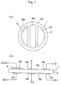
- Fig. 1 (a) is a plan view schematically showing a device 1 for measuring a mass
- Fig. 1 (b) is a front view showing the device of Fig. 1(a).
- Figs. 2 (a) and 2 (b) are plan and perspective views, respectively, for explaining thickness-twist vibration mode
- Fig. 3 shows an example of a circuit.
- a device of the present example has a vibrator 2 substantially having a shape of a disk.
- Driving electrodes 3A and 3B and a detecting electrode 4A are formed on a surface 2a of the vibrator 2.
- Driving electrodes 3C, 3D and a detecting electrode 4B are formed on a surface 2b of the vibrator 2.
- the driving electrode 3B is covered with an adsorption film 5.
- a driving power source 8 in a driving circuit unit 14 is used to apply alternating current voltages of inverse phases between the driving electrodes 3A and 3C and between the driving electrodes 3B and 3D. Thickness-shear vibration is thereby induced as arrows "A" and "B” shown in Figs.
- Driving vibration modes “A” and “B” are substantially symmetrical with respect to the central axis "D" of the vibrator.
- Dislocation of the vibrator in a region between the detecting electrodes 4A and 4B results in a voltage generated between a signal terminal "P" and a ground terminal "PG".
- the difference of potential is detected with a detection amplifier 9 in a signal processing part 6 and then subjected to phase detection with driving vibration by means of a phase detection circuit 10.
- the vibration having the same phase as the driving vibration mode is supplied to a low path filter 11 and output.
- Detection signals output from central detecting electrodes 4A and 4B are adjusted at substantially zero when a mass is not to be measured.
- the dislocations "A" and “B” of the driving vibration are substantially symmetrical with respect to the central axis "D" of the vibrator 2, so that the dislocation of vibration of the vibrator in a region between the detecting electrodes 4A and 4B are designed to be substantially zero.
- the mass of the adsorption film 5 is increased so that the balance of mass in both sides of the central axis "D" of the vibrator is lost.
- the driving vibration modes "A” and “B” are made not symmetrical with respect to the central axis "D” so that a signal voltage having the same phase as the driving vibration is induced between the detecting electrodes 4A and 4B.
- a mass is calculated based on the signal voltage.
- Fig. 4 (a) is a plan view schematically showing a device 21 for measuring a mass according to another embodiment
- Fig. 4 (b) is a front view of the device 21.
- the device has a vibrator 2 having a shape of, for example, a disk.
- Driving electrodes 3A and 3B and a detecting electrode 4A are formed on a surface 2a of the vibrator 2.
- a ground electrode 14 and a driving (ground) electrode 3C are formed on a surface 2b of the vibrator 2.
- the driving electrode 3B is covered with an adsorption film 5.
- a driving power source 8 in a driving circuit unit 14 is used to apply alternating current voltages of inverse phases between the driving electrodes 3A and 3C and between the driving electrode 3B and the ground electrode 14.
- Thickness-shear vibration is thereby induced as arrows "A” and “B” shown in Figs. 2(a) and 2 (b).
- "D1” and “D2” represent terminals for applying alternating current voltages, respectively, and
- “D1G” and “G” represent ground terminals, respectively.
- Driving vibration modes “A” and “B” are substantially symmetrical with respect to the central axis "D" of the vibrator.
- Dislocation of the vibrator in a region between the detecting electrodes 4A and 14 results in a voltage generated between a signal terminal "P" and a ground terminal "G".
- the difference of potential is detected with a detection amplifier 9 in a signal processing part 6 and then subjected to phase detection with driving vibration by means of a phase detection circuit 10.
- the vibration having the same phase as the driving vibration mode is supplied to a low path filter 11 and output. Detection signals output from the central detecting electrodes 4A and 14 are adjusted at substantially zero when a mass is not to be measured.
- the mass of the adsorption film 5 is increased so that the balance of mass in both sides of the central axis "D" of the vibrator is lost.
- the driving vibration modes "A” and “B” are made not symmetrical with respect to the central axis "D” so that a signal voltage having the same phase as the driving vibration is induced between the detecting electrodes 4A and 14. A mass is calculated based on the signal voltage.
- a vibrator has at least one pair of bending vibration arms, and the basic vibration mode includes bending vibration of the bending vibration arm. Dislocation can be made large in such bending mode so that the embodiment is effective for further improving the sensitivity.
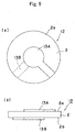
- Fig. 5 is a plan view schematically showing a vibrator (before an adsorption film is formed thereon) according to the present embodiment
- Fig. 6 is a plan view schematically showing a vibrator 31 (after an adsorption film is formed thereon) according to the present embodiment.
- the vibrator 45 has a base part 34 having a square shape of quad-symmetrical with respect to the center of gravity GO (the center of gravity when the vibrator is not vibrated) of the vibrator.
- a pair of elongate supporting portions 35 are protruded from the peripheral part of the base portion 34 substantially symmetrical with respect to the center "D”.
- a pair of bending vibration arms 36A and 36B or 36C and 36D are protruded from the end of each of the supporting portions 35 in a direction substantially parallel with the central axis "D".
- a wide weight or hammerhead portion is provided at each end of each of the bending vibration arms 36A to 36D.
- a through hole is formed in each weight portion.
- Driving electrodes 32, 33A and 33B are formed on the side and main faces of each bending vibration arm.
- Elongate detection vibration arms 38A and 38B are protruded from the peripheral part of the base portion 34 in a direction of the central axis "D".
- a wide weight or hammerhead portion is provided at each end of each of the detection vibration arms 38A and 38B.
- a through hole is formed in each weight portion.
- Detecting electrodes 39 and 40 are formed on the side and main faces of each detection vibration arm.
- adsorption films 41A and 41B are formed so that they cover electrodes 33A on the driving vibration arms on the right side on the figure.
- the driving electrodes are used to excite driving vibration in which each of the driving vibration arms 36A, 36B, 36c and 36d vibrates in bending motion around the end of the supporting portion 35 as the fulcrum as an arrow "E".
- the dislocation of vibration of the bending vibration arms 36A and 36B and that of the bending vibration arms 36C, and 36D are made substantially symmetrical with respect to the central axis "D".
- the center of gravity "GD" of the whole of the driving vibration of the arms 36A, 36B, 36C and 36D, as well as the center of gravity "GO” of the vibrator, are substantially located on the central axis "D".
- the detection currents in the detecting electrodes 39 and 40 on detecting vibration arms 38A and 38B are adjusted substantially at zero.
- the material of the vibrator is not particularly limited and may preferably be a piezoelectric single crystal such as quartz, LiNbO 3 , LiTaO 3 , lithium niobate-lithium tantalate solid solution (Li(Nb, Ta)O 3 ) single crystal, lithium borate single crystal or langasite single crystal.
- a piezoelectric single crystal such as quartz, LiNbO 3 , LiTaO 3 , lithium niobate-lithium tantalate solid solution (Li(Nb, Ta)O 3 ) single crystal, lithium borate single crystal or langasite single crystal.
- Each of the electrodes may be composed of a conductive film.
- Such conductive film may preferably be a metal film such as a gold film, a multilayer film of gold and chromium, a multilayer film of gold and titanium, silver film, a multilayer film of silver and chromium, a multilayer film of silver and titanium, a lead film or platinum film, or a metal oxide film such as TiO 2 .
- a gold film has poor adherence with an oxide single crystal film such as quartz film, however, it is preferred to provide an underlayer such as chromium or titanium film between the vibration arm such as an arm made of quartz and the gold film.
- Materials for the adsorption film are not particularly limited and may be one or more of the followings.
- the adsorption film may be produced by any process such as dipping or spin coating.
- Substances to be adsorbed include the followings.
- Odors such as isoamyl acetate, phenyl ethyl alcohol, p-anisaldehyde, citral, geraniol, phenyl ethyl alcohol, ⁇ -terpeneol etc.: environmental hormones such as dioxine: biosubstances such as protein, DNA, antigen, antibody etc.: chemical substances such as glucose, alcohol, urea, uric acid, lactic acid etc.
- the detecting means of the dislocation of vibration may preferably be a detecting electrode as described above, it is not particularly limited.
- the dislocation of the vibrator on the central axis and its neighboring part may be measured with a laser displacement meter.
- the width "L" of the driving electrode is 0.2 times or more and 4.0 times or less of the width "M" of the detecting electrode. It is possible to improve the Q value of driving vibration by the driving electrodes and the sensitivity of detection, by adjusting the width of the driving electrode for exciting the basic vibration mode at a value of 0.2 times or more and 4,0 times or less of the width of the detecting electrode for measuring the dislocation of vibration.
- the width "L” of the driving electrode may more preferably be 0.3 times or more of the width "M” of the detecting electrode. Further, the width “L” of the driving electrode may more preferably be 2.0 times or less of the width "M” of the detecting electrode.
- the area "N" of the driving electrode may preferably be 0.1 to 3.0 times of the area "O" of the detecting electrode, so that the Q-value of the driving vibration and the sensitivity of detection can be similarly improved.
- the area "N" of the driving electrode means the area of each driving electrode.
- the area "O" of the detecting electrode means the area of each detecting electrode.
- the area "N" of the driving electrode may more preferably be 0.2 times or more of the area “O" of the detecting electrode. Further, the area “N" of the driving electrode may more preferably be 1.5 times or less of the area “O” of the detecting electrode.
- Fig. 7 (a) is a plan view schematically showing a device 1A for measuring a mass according to the present embodiment
- Fig. 7(b) is a cross sectional view showing the device of Fig. 7(a).
- the present device has a vibrator 2 substantially having a shape of a disk.
- Driving electrodes 3A and 3B and a detecting electrode 4A are formed on a surface 2a of the vibrator 2.
- Driving electrodes 3C, 3D and a detecting electrode 4B are formed on a surface 2b of the vibrator 2.
- the driving electrode 3B is covered with an adsorption film 5.
- a driving power source 8 in a driving circuit unit 14 is used to apply alternating current voltages of inverse phases between the driving electrodes 3A and 3C and between the driving electrodes 3B and 3D. Thickness-shear vibration is thereby induced as arrows "A" and "B” shown in Figs. 2(a) and 2 (b).
- Dislocation of the vibrator in a region between the detecting electrodes 4A and 4B results in a voltage generated between a signal terminal "P" and a ground terminal "PG".
- the difference of potential is detected with a detection amplifier 9 in a signal processing part 6 and then subjected to phase detection with driving vibration by means of a phase detection circuit 10.
- the vibration having the same phase as the driving vibration mode is supplied to a low path filter 11 and output.
- the following procedure is the same as that used in the device shown in Figs. 1 to 3.
- the width "L" of each of the driving electrodes 3A and 3C is made 0.2 times or more and 4.0 times or less of the width "M" of the detecting electrode 4A.
- the area “N" of the each of the driving electrodes 3A and 3C is made 0.1 times or more and 3.0 times or less of the area "O" of the detecting electrode 4A.
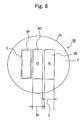
- Fig. 8 is a plan view schematically showing a device 1B for measuring a mass according to the present embodiment.
- the device of the present example has a vibrator 2 having a shape of, for example, a disk.
- Driving electrodes 3E and 3F and a detecting electrode 4C are formed on a surface 2a of the vibrator 2.
- Each of the driving and detecting electrodes has a rectangular shape.
- the driving electrode 3F is covered with an adsorption film 5.
- the procedure of detection using the vibrator 2 is the same as that in the examples shown in Figs. 2 (a) and 2 (b) and Figs. 7 (a) and 7 (b).
- the width "L" of each of the driving electrodes 3E and 3F is made 0.2 times or more and 4.0 times or less of the width "M" of the detecting electrode 4C.
- the area “N" of each of the driving electrodes 3E and 3F is made 0.1 times or more and 3.0 times or less of the area "O" of the detecting electrode 4C.
- the measuring device 1 shown in Figs. 1 to 3 was produced.
- the vibrator 2 was formed of an AT cut quartz plate.
- the vibrator 2 has a diameter of 9 mm and a thickness of 0.083 mm.
- the electrodes are formed of chromium/gold film (thickness of 500 angstrom).
- the adsorption film 5 was formed by patterning using a mask followed by dipping. The adsorption of a mass of 1 pg can be successfully detected.
- the device for measuring shown in Figs. 5 and 6 was produced.
- the vibrator had a dimension of 2 mm and 2 mm and a thickness of 0.1 mm.
- the characteristic resonance frequency of the driving vibration was 50 kHz.
- a change of detected voltage of 1 ⁇ V was obtained for the adsorption of a mass of 1 pg at a driving signal voltage of 10 volts.
- the sensitivity is sufficiently high for detecting the adsorption of a mass of 1 pg.
- the measuring device 1A shown in Figs. 7, 2 and 3 was produced.
- the vibrator 2 was formed of an AT cut quartz plate.
- the vibrator 2 has a diameter of 9 mm and a thickness of 0.160 mm.
- the electrodes are formed of chromium/gold film (thickness of 200/1000 angstrom).
- the adsorption film 5 was formed by patterning using a mask followed by dipping.
- the ratio (L/M) of the width "L” of the driving electrode with respect to the width "M” of the detecting electrode was changed as shown in table 2.
- the Q value of detection in the detecting electrode was measured and the results were shown in table 2.
- Width "L” of driving electrode/ Width “M” of detecting electrode Q value of driving vibration 0.13 11,000 0.17 29,000 0.20 31,000 0.25 42,000 0.30 50,000 0.5 70,000 1.0 78,000 1.1 42,000 2.0 53,000 2.2 28,000 3.0 42,000 4.0 32,000 4.2 16,000 4.7 26,000 6.5 19,000 10.5 9,000
- the measuring device 1A shown in Figs. 7, 2 and 3 was produced.
- the vibrator 2 was formed of an AT cut quartz plate.
- the vibrator 2 has a diameter of 9 mm and a thickness of 0.160 mm.
- the electrodes were formed of chromium/gold film (thickness of 200/1000 angstrom).
- the adsorption film 5 was formed by patterning using a mask followed by dipping.
- a device 1 for measuring a mass comprises a vibrator 2, driving means 3A, 3B, 3C, 3D for exciting a basic vibration in the vibrator 2, detecting means 4A, 4B for detecting a displacement of vibration in the vibrator 2 and an adsorption film 5 capable of adsorbing a substance for detection.
- the mass is measured based on a difference between a detected value of the displacement of vibration obtained from the detecting means 4A, 4B when the mass is not measured and a detected value of the displacement of vibration obtained from the detecting means 4A, 4B when the mass is measured.
Landscapes
- Physics & Mathematics (AREA)
- General Physics & Mathematics (AREA)
- Biochemistry (AREA)
- Life Sciences & Earth Sciences (AREA)
- Chemical & Material Sciences (AREA)
- Analytical Chemistry (AREA)
- Health & Medical Sciences (AREA)
- General Health & Medical Sciences (AREA)
- Acoustics & Sound (AREA)
- Immunology (AREA)
- Pathology (AREA)
- Measurement Of Mechanical Vibrations Or Ultrasonic Waves (AREA)
- Piezo-Electric Or Mechanical Vibrators, Or Delay Or Filter Circuits (AREA)
- Investigating Or Analyzing Materials By The Use Of Ultrasonic Waves (AREA)
Applications Claiming Priority (4)
| Application Number | Priority Date | Filing Date | Title |
|---|---|---|---|
| JP2003295012 | 2003-08-19 | ||
| JP2003295012 | 2003-08-19 | ||
| JP2004199214 | 2004-07-06 | ||
| JP2004199214A JP4222513B2 (ja) | 2003-08-19 | 2004-07-06 | 質量測定装置および方法 |
Publications (2)
| Publication Number | Publication Date |
|---|---|
| EP1508802A2 true EP1508802A2 (de) | 2005-02-23 |
| EP1508802A3 EP1508802A3 (de) | 2005-04-06 |
Family
ID=34067412
Family Applications (1)
| Application Number | Title | Priority Date | Filing Date |
|---|---|---|---|
| EP04019563A Withdrawn EP1508802A3 (de) | 2003-08-19 | 2004-08-18 | Vorrichtung und Methode zur Bestimmung der Masse einer zu bestimmenden Substanz, enthaltend ein vibrierendes Element mit einem Adsorptionsfilm |
Country Status (4)
| Country | Link |
|---|---|
| US (1) | US7140255B2 (de) |
| EP (1) | EP1508802A3 (de) |
| JP (1) | JP4222513B2 (de) |
| CN (1) | CN100494893C (de) |
Cited By (1)
| Publication number | Priority date | Publication date | Assignee | Title |
|---|---|---|---|---|
| CN104541148A (zh) * | 2012-08-10 | 2015-04-22 | 富士通株式会社 | Qcm传感器及其制造方法 |
Families Citing this family (22)
| Publication number | Priority date | Publication date | Assignee | Title |
|---|---|---|---|---|
| SE0300375D0 (sv) * | 2003-02-12 | 2003-02-12 | Attana Ab | Piezoelectric resonator |
| US7075216B1 (en) * | 2004-03-31 | 2006-07-11 | University Of Maine System Board Of Trustees | Lateral field excited acoustic wave sensor |
| JP4803802B2 (ja) * | 2005-02-14 | 2011-10-26 | 日本碍子株式会社 | 質量測定装置 |
| JP2007187485A (ja) * | 2006-01-11 | 2007-07-26 | National Institute Of Advanced Industrial & Technology | 検出センサ |
| JP4540057B2 (ja) * | 2005-06-06 | 2010-09-08 | 日本碍子株式会社 | スート検出装置 |
| JP4535501B2 (ja) * | 2005-06-06 | 2010-09-01 | 日本碍子株式会社 | 塩素イオン検出装置 |
| JP4535502B2 (ja) * | 2005-06-28 | 2010-09-01 | 日本碍子株式会社 | 物質検出素子 |
| JP4530361B2 (ja) * | 2005-06-29 | 2010-08-25 | 日本碍子株式会社 | 物質検出素子の製造方法 |
| JP4707104B2 (ja) * | 2005-10-31 | 2011-06-22 | 日本碍子株式会社 | 振動素子の製造方法 |
| DE102006039858A1 (de) * | 2006-01-02 | 2007-07-12 | Ceramtec Ag Innovative Ceramic Engineering | Monolithisches Biegeelement |
| US7681449B2 (en) * | 2006-02-28 | 2010-03-23 | Exxonmobil Research And Engineering Company | Metal loss rate sensor and measurement using a mechanical oscillator |
| US20070236213A1 (en) * | 2006-03-30 | 2007-10-11 | Paden Bradley E | Telemetry method and apparatus using magnetically-driven mems resonant structure |
| JP2008102119A (ja) * | 2006-06-30 | 2008-05-01 | Univ Of Maine System | モノリシック・アンテナ励起音響変換装置 |
| JP2009085777A (ja) * | 2007-09-28 | 2009-04-23 | National Institute Of Advanced Industrial & Technology | 振動子チップ、検出センサ |
| JP5066551B2 (ja) * | 2008-05-20 | 2012-11-07 | 日本電波工業株式会社 | 圧電センサ及び感知装置 |
| JP2010078345A (ja) * | 2008-09-24 | 2010-04-08 | National Institute Of Advanced Industrial Science & Technology | 検出センサ、振動子 |
| JP2010078334A (ja) * | 2008-09-24 | 2010-04-08 | National Institute Of Advanced Industrial Science & Technology | 検出センサ、振動子 |
| CN101968359B (zh) * | 2010-07-02 | 2011-11-09 | 北京理工大学 | 钟形振子式角速率陀螺 |
| US9322701B2 (en) | 2013-08-02 | 2016-04-26 | Qualcomm Incorporated | Dynamic force sensing to determine mass using a smartphone |
| CN105953873A (zh) * | 2016-06-13 | 2016-09-21 | 常州大学 | 利用光学静态测量dna分子质量的方法 |
| JP6871823B2 (ja) * | 2017-08-10 | 2021-05-12 | ヤンマーパワーテクノロジー株式会社 | 果実生育監視システム、及び果実生育監視方法 |
| CN107643228B (zh) * | 2017-08-31 | 2021-04-27 | 中国船舶重工集团公司第七一九研究所 | 一种测量汞蒸气的芯片的制备方法及其传感器的使用方法 |
Citations (1)
| Publication number | Priority date | Publication date | Assignee | Title |
|---|---|---|---|---|
| US20020115198A1 (en) * | 2000-09-20 | 2002-08-22 | Nerenberg Michael I. | Microfabricated ultrasound array for use as resonant sensors |
Family Cites Families (17)
| Publication number | Priority date | Publication date | Assignee | Title |
|---|---|---|---|---|
| JPS534940A (en) * | 1976-07-01 | 1978-01-18 | Shimano Industrial Co | Bicycle handle controller |
| US4361026A (en) * | 1980-06-24 | 1982-11-30 | Muller Richard S | Method and apparatus for sensing fluids using surface acoustic waves |
| US4549427A (en) * | 1983-09-19 | 1985-10-29 | The United States Of America As Represented By The Secretary Of The Air Force | Electronic nerve agent detector |
| DE3650562T2 (de) * | 1985-04-11 | 1997-03-20 | Toyo Communication Equip | Piezoelektrischer resonator zur erzeugung von oberschwingungen |
| US4999284A (en) * | 1988-04-06 | 1991-03-12 | E. I. Du Pont De Nemours And Company | Enzymatically amplified piezoelectric specific binding assay |
| US5112642A (en) * | 1990-03-30 | 1992-05-12 | Leybold Inficon, Inc. | Measuring and controlling deposition on a piezoelectric monitor crystal |
| JP3139562B2 (ja) | 1992-02-17 | 2001-03-05 | 日本電信電話株式会社 | におい質センシング方法 |
| JPH05346384A (ja) | 1992-06-16 | 1993-12-27 | Nippon Telegr & Teleph Corp <Ntt> | においセンサヘッド |
| US6912901B1 (en) * | 1995-05-30 | 2005-07-05 | Matsushita Electric Industrial Co., Ltd. | Angular velocity sensor |
| US5719324A (en) * | 1995-06-16 | 1998-02-17 | Lockheed Martin Energy Systems, Inc. | Microcantilever sensor |
| WO1998041835A1 (fr) * | 1997-03-17 | 1998-09-24 | Hitachi, Ltd. | Dispositif excitateur de vibrations et dispositif testeur de vibrations pour structures, utilisant ledit dispositif |
| JP3298898B2 (ja) * | 1997-12-26 | 2002-07-08 | 日本碍子株式会社 | 双頭型質量センサおよびその質量検出方法 |
| GB9819319D0 (en) * | 1998-09-05 | 1998-10-28 | Aea Technology Plc | Assay of chemical binding |
| US6575020B1 (en) * | 1999-05-03 | 2003-06-10 | Cantion A/S | Transducer for microfluid handling system |
| CA2417939A1 (en) * | 2000-08-09 | 2002-02-14 | California Institute Of Technology | Active nems arrays for biochemical analyses |
| US6526835B1 (en) * | 2001-06-06 | 2003-03-04 | Andersen Corporation | Apparatus and method for characterizing physical properties of a test piece |
| JP2004028956A (ja) | 2002-06-28 | 2004-01-29 | National Institute Of Advanced Industrial & Technology | 吸脱着量測定方法及び装置 |
-
2004
- 2004-07-06 JP JP2004199214A patent/JP4222513B2/ja not_active Expired - Fee Related
- 2004-08-13 US US10/918,206 patent/US7140255B2/en not_active Expired - Fee Related
- 2004-08-18 EP EP04019563A patent/EP1508802A3/de not_active Withdrawn
- 2004-08-19 CN CNB2004100766040A patent/CN100494893C/zh not_active Expired - Fee Related
Patent Citations (1)
| Publication number | Priority date | Publication date | Assignee | Title |
|---|---|---|---|---|
| US20020115198A1 (en) * | 2000-09-20 | 2002-08-22 | Nerenberg Michael I. | Microfabricated ultrasound array for use as resonant sensors |
Cited By (1)
| Publication number | Priority date | Publication date | Assignee | Title |
|---|---|---|---|---|
| CN104541148A (zh) * | 2012-08-10 | 2015-04-22 | 富士通株式会社 | Qcm传感器及其制造方法 |
Also Published As
| Publication number | Publication date |
|---|---|
| EP1508802A3 (de) | 2005-04-06 |
| CN100494893C (zh) | 2009-06-03 |
| US7140255B2 (en) | 2006-11-28 |
| JP4222513B2 (ja) | 2009-02-12 |
| US20050039532A1 (en) | 2005-02-24 |
| JP2005098986A (ja) | 2005-04-14 |
| CN1609555A (zh) | 2005-04-27 |
Similar Documents
| Publication | Publication Date | Title |
|---|---|---|
| EP1508802A2 (de) | Vorrichtung und Methode zur Bestimmung der Masse einer zu bestimmenden Substanz, enthaltend ein vibrierendes Element mit einem Adsorptionsfilm | |
| EP0775295B1 (de) | Piezoelektrische quarz-mikrowaage | |
| US7207222B2 (en) | Electromagnetic piezoelectric acoustic sensor | |
| US6033852A (en) | Monolithic piezoelectric sensor (MPS) for sensing chemical, biochemical and physical measurands | |
| EP1533611B1 (de) | Vorrichtung und Verfahren zur Messung von Mikrogewichten mittels eines Schwingkreises | |
| US5684276A (en) | Micromechanical oscillating mass balance | |
| US9023283B2 (en) | Resonant type mass sensor | |
| US20060064259A1 (en) | Technique and electronic circuitry for quantifying a transient signal using threshold-crossing counting to track signal amplitude | |
| JP2001083060A (ja) | 化学センサー用ポリマーコーティング | |
| SE520046C2 (sv) | Förfarande för att mäta växelverkan mellan en målmolekyl och en receptormolekyl med piezoelektrisk kristallmikrovåg | |
| Ferrari et al. | Multisensor array of mass microbalances for chemical detection based on resonant piezo-layers of screen-printed PZT | |
| US20080163689A1 (en) | Electromagnetic piezoelectric acoustic sensor | |
| JP2004093574A (ja) | 原子間力顕微鏡用力方位センサ付カンチレバー | |
| JP4415365B2 (ja) | 振動子の検出離調の測定方法およびその調整方法 | |
| WO2006082668A1 (ja) | バイオセンサ及びバイオセンサチップ | |
| US20100199746A1 (en) | Cantilever Type Sensor | |
| Cumpson | Quartz crystal microbalance: A new design eliminates sensitivity outside the electrodes, often wrongly attributed to the electric fringing field | |
| JP4803802B2 (ja) | 質量測定装置 | |
| JP4535502B2 (ja) | 物質検出素子 | |
| JP4222511B2 (ja) | 質量検出素子 | |
| JP4535501B2 (ja) | 塩素イオン検出装置 | |
| JP4530361B2 (ja) | 物質検出素子の製造方法 | |
| JP4707104B2 (ja) | 振動素子の製造方法 | |
| CN116915204A (zh) | 用于提高耦合的具有厚介电层的横向激发薄膜体声学谐振器 | |
| Mølgaard | Capacitive Micromachined Ultrasonic Transducers for Gas Sensing |
Legal Events
| Date | Code | Title | Description |
|---|---|---|---|
| PUAI | Public reference made under article 153(3) epc to a published international application that has entered the european phase |
Free format text: ORIGINAL CODE: 0009012 |
|
| PUAL | Search report despatched |
Free format text: ORIGINAL CODE: 0009013 |
|
| AK | Designated contracting states |
Kind code of ref document: A2 Designated state(s): AT BE BG CH CY CZ DE DK EE ES FI FR GB GR HU IE IT LI LU MC NL PL PT RO SE SI SK TR |
|
| AX | Request for extension of the european patent |
Extension state: AL HR LT LV MK |
|
| AK | Designated contracting states |
Kind code of ref document: A3 Designated state(s): AT BE BG CH CY CZ DE DK EE ES FI FR GB GR HU IE IT LI LU MC NL PL PT RO SE SI SK TR |
|
| AX | Request for extension of the european patent |
Extension state: AL HR LT LV MK |
|
| 17P | Request for examination filed |
Effective date: 20051005 |
|
| AKX | Designation fees paid |
Designated state(s): DE FR GB |
|
| 17Q | First examination report despatched |
Effective date: 20110805 |
|
| STAA | Information on the status of an ep patent application or granted ep patent |
Free format text: STATUS: THE APPLICATION IS DEEMED TO BE WITHDRAWN |
|
| 18D | Application deemed to be withdrawn |
Effective date: 20180301 |
|
| RIC1 | Information provided on ipc code assigned before grant |
Ipc: G01G 3/16 20060101ALI20041215BHEP Ipc: G01N 27/00 20060101AFI20041215BHEP |