EP1498216A1 - Method of cutting processed object - Google Patents
Method of cutting processed object Download PDFInfo
- Publication number
- EP1498216A1 EP1498216A1 EP03744054A EP03744054A EP1498216A1 EP 1498216 A1 EP1498216 A1 EP 1498216A1 EP 03744054 A EP03744054 A EP 03744054A EP 03744054 A EP03744054 A EP 03744054A EP 1498216 A1 EP1498216 A1 EP 1498216A1
- Authority
- EP
- European Patent Office
- Prior art keywords
- cutting
- region
- cut
- starting point
- processed
- Prior art date
- Legal status (The legal status is an assumption and is not a legal conclusion. Google has not performed a legal analysis and makes no representation as to the accuracy of the status listed.)
- Granted
Links
Images





Classifications
-
- H—ELECTRICITY
- H10—SEMICONDUCTOR DEVICES; ELECTRIC SOLID-STATE DEVICES NOT OTHERWISE PROVIDED FOR
- H10P—GENERIC PROCESSES OR APPARATUS FOR THE MANUFACTURE OR TREATMENT OF DEVICES COVERED BY CLASS H10
- H10P54/00—Cutting or separating of wafers, substrates or parts of devices
-
- B—PERFORMING OPERATIONS; TRANSPORTING
- B23—MACHINE TOOLS; METAL-WORKING NOT OTHERWISE PROVIDED FOR
- B23K—SOLDERING OR UNSOLDERING; WELDING; CLADDING OR PLATING BY SOLDERING OR WELDING; CUTTING BY APPLYING HEAT LOCALLY, e.g. FLAME CUTTING; WORKING BY LASER BEAM
- B23K26/00—Working by laser beam, e.g. welding, cutting or boring
- B23K26/36—Removing material
- B23K26/40—Removing material taking account of the properties of the material involved
-
- B—PERFORMING OPERATIONS; TRANSPORTING
- B23—MACHINE TOOLS; METAL-WORKING NOT OTHERWISE PROVIDED FOR
- B23K—SOLDERING OR UNSOLDERING; WELDING; CLADDING OR PLATING BY SOLDERING OR WELDING; CUTTING BY APPLYING HEAT LOCALLY, e.g. FLAME CUTTING; WORKING BY LASER BEAM
- B23K26/00—Working by laser beam, e.g. welding, cutting or boring
- B23K26/36—Removing material
- B23K26/38—Removing material by boring or cutting
-
- B—PERFORMING OPERATIONS; TRANSPORTING
- B23—MACHINE TOOLS; METAL-WORKING NOT OTHERWISE PROVIDED FOR
- B23K—SOLDERING OR UNSOLDERING; WELDING; CLADDING OR PLATING BY SOLDERING OR WELDING; CUTTING BY APPLYING HEAT LOCALLY, e.g. FLAME CUTTING; WORKING BY LASER BEAM
- B23K26/00—Working by laser beam, e.g. welding, cutting or boring
- B23K26/36—Removing material
- B23K26/38—Removing material by boring or cutting
- B23K26/382—Removing material by boring or cutting by boring
- B23K26/384—Removing material by boring or cutting by boring of specially shaped holes
-
- B—PERFORMING OPERATIONS; TRANSPORTING
- B23—MACHINE TOOLS; METAL-WORKING NOT OTHERWISE PROVIDED FOR
- B23K—SOLDERING OR UNSOLDERING; WELDING; CLADDING OR PLATING BY SOLDERING OR WELDING; CUTTING BY APPLYING HEAT LOCALLY, e.g. FLAME CUTTING; WORKING BY LASER BEAM
- B23K26/00—Working by laser beam, e.g. welding, cutting or boring
- B23K26/50—Working by transmitting the laser beam through or within the workpiece
- B23K26/53—Working by transmitting the laser beam through or within the workpiece for modifying or reforming the material inside the workpiece, e.g. for producing break initiation cracks
-
- B—PERFORMING OPERATIONS; TRANSPORTING
- B28—WORKING CEMENT, CLAY, OR STONE
- B28D—WORKING STONE OR STONE-LIKE MATERIALS
- B28D1/00—Working stone or stone-like materials, e.g. brick, concrete or glass, not provided for elsewhere; Machines, devices, tools therefor
- B28D1/22—Working stone or stone-like materials, e.g. brick, concrete or glass, not provided for elsewhere; Machines, devices, tools therefor by cutting, e.g. incising
- B28D1/221—Working stone or stone-like materials, e.g. brick, concrete or glass, not provided for elsewhere; Machines, devices, tools therefor by cutting, e.g. incising by thermic methods
-
- B—PERFORMING OPERATIONS; TRANSPORTING
- B28—WORKING CEMENT, CLAY, OR STONE
- B28D—WORKING STONE OR STONE-LIKE MATERIALS
- B28D5/00—Fine working of gems, jewels, crystals, e.g. of semiconductor material; apparatus or devices therefor
- B28D5/0005—Fine working of gems, jewels, crystals, e.g. of semiconductor material; apparatus or devices therefor by breaking, e.g. dicing
- B28D5/0011—Fine working of gems, jewels, crystals, e.g. of semiconductor material; apparatus or devices therefor by breaking, e.g. dicing with preliminary treatment, e.g. weakening by scoring
-
- C—CHEMISTRY; METALLURGY
- C03—GLASS; MINERAL OR SLAG WOOL
- C03B—MANUFACTURE, SHAPING, OR SUPPLEMENTARY PROCESSES
- C03B33/00—Severing cooled glass
- C03B33/02—Cutting or splitting sheet glass or ribbons; Apparatus or machines therefor
- C03B33/0222—Scoring using a focussed radiation beam, e.g. laser
-
- C—CHEMISTRY; METALLURGY
- C03—GLASS; MINERAL OR SLAG WOOL
- C03B—MANUFACTURE, SHAPING, OR SUPPLEMENTARY PROCESSES
- C03B33/00—Severing cooled glass
- C03B33/02—Cutting or splitting sheet glass or ribbons; Apparatus or machines therefor
- C03B33/023—Cutting or splitting sheet glass or ribbons; Apparatus or machines therefor the sheet or ribbon being in a horizontal position
- C03B33/033—Apparatus for opening score lines in glass sheets
-
- C—CHEMISTRY; METALLURGY
- C03—GLASS; MINERAL OR SLAG WOOL
- C03B—MANUFACTURE, SHAPING, OR SUPPLEMENTARY PROCESSES
- C03B33/00—Severing cooled glass
- C03B33/07—Cutting armoured, multi-layered, coated or laminated, glass products
-
- C—CHEMISTRY; METALLURGY
- C03—GLASS; MINERAL OR SLAG WOOL
- C03B—MANUFACTURE, SHAPING, OR SUPPLEMENTARY PROCESSES
- C03B33/00—Severing cooled glass
- C03B33/07—Cutting armoured, multi-layered, coated or laminated, glass products
- C03B33/074—Glass products comprising an outer layer or surface coating of non-glass material
-
- B—PERFORMING OPERATIONS; TRANSPORTING
- B23—MACHINE TOOLS; METAL-WORKING NOT OTHERWISE PROVIDED FOR
- B23K—SOLDERING OR UNSOLDERING; WELDING; CLADDING OR PLATING BY SOLDERING OR WELDING; CUTTING BY APPLYING HEAT LOCALLY, e.g. FLAME CUTTING; WORKING BY LASER BEAM
- B23K2101/00—Articles made by soldering, welding or cutting
- B23K2101/36—Electric or electronic devices
- B23K2101/40—Semiconductor devices
-
- B—PERFORMING OPERATIONS; TRANSPORTING
- B23—MACHINE TOOLS; METAL-WORKING NOT OTHERWISE PROVIDED FOR
- B23K—SOLDERING OR UNSOLDERING; WELDING; CLADDING OR PLATING BY SOLDERING OR WELDING; CUTTING BY APPLYING HEAT LOCALLY, e.g. FLAME CUTTING; WORKING BY LASER BEAM
- B23K2103/00—Materials to be soldered, welded or cut
- B23K2103/50—Inorganic materials other than metals or composite materials
Definitions
- the present invention relates to a method of cutting an object to be processed for cutting an object to be processed such as a semiconductor material substrate, a piezoelectric substrate, and a glass substrate.
- One of laser applications is cutting.
- the following is typical cutting by laser.
- a part to cut in an object to be processed such as a semiconductor wafer or glass substrate is irradiated with laser light having a wavelength absorbed by the object, and melting by heating is advanced by the laser light absorption from the front face to rear face of the object in the part to cut, so as to cut the object.
- this method also melts the surroundings of a region which becomes a part to cut in the front face of the object.
- the object to be processed is a semiconductor wafer, there is a fear of semiconductor devices positioned near the above-mentioned region among those formed on the front face of the semiconductor wafer melting.
- Examples of methods of preventing the front face of such an object to be processed from melting include laser cutting methods disclosed in Japanese Patent Application Laid-Open Nos. 2000-219528 and 2000-15467.
- the cutting methods of these publications cause laser light to heat a part to cut in the object to be processed, and then cool the object, so as to generate a thermal shock at the part to cut in the object, thereby cutting the object.
- an object of the present invention to provide a method of cutting an object to be processed which can accurately cut the object.
- the method of cutting an object to be processed in accordance with the present invention comprises a starting point region for cutting forming step of irradiating a wafer-like object to be processed with laser light while positioning a light-converging point therewithin, so as to form a modified region due to multiphoton absorption within the object, and causing the modified region to form a starting point region for cutting, deviated from a center position of the object in a thickness direction thereof toward one end face of the object, along a line along which the object should be cut in the object; and a pressing step of pressing the object from the other end face side of the object.
- the modified region formed by multiphoton absorption forms a starting point region for cutting within the object along a desirable line along which the object should be cut for cutting the object.
- the multiphoton absorption occurs locally within the object, so that laser light is hardly absorbed by one end face of the object and the other end face on the opposite side thereof, whereby one end face and the other end face can be prevented from melting upon laser light irradiation.
- the starting point region for cutting is formed so as to deviate from the center position of the object in the thickness direction thereof toward one end face, when the object is pressed from the other end face side, a fracture can be generated in the object from the starting point region for cutting acting as a start point with a pressing force smaller than that in the case where the starting point region for cutting is formed at the center position. This can prevent unnecessary fractures deviated from the line along which the object should be cut from occurring, and accurately cut the object along the line along which the object should be cut.
- the light-converging point refers to a location at which laser light is converged.
- the starting point region for cutting refers to a region to become a start point for cutting when the object to be processed is cut. Therefore, the starting point region for cutting is a part to cut where cutting is to be performed in the object.
- the starting point region for cutting may be produced by continuously forming a modified region or intermittently forming a modified region.
- the expression "form a starting point region for cutting deviated from a center position of the object in a thickness direction thereof toward one end face of the object” means that a modified region constituting the starting point region for cutting is formed so as to deviate from the half thickness position of the object in the thickness direction thereof toward one end face.
- the center position of the width of the modified region (starting point region for cutting) in the thickness direction of the object is positioned so as to deviate from the center position of the object in the thickness direction toward one end face, and is not limited to the case where the whole modified region (starting point region for cutting) is positioned on the one end face side of the center position of the object in the thickness direction.
- the pressing step presses the object along the line along which the object should be cut.
- the object can accurately be cut into the functional devices if a line along which the object should be cut is set between neighboring functional devices and the object is pressed along this line along which the object should be cut. Also, this can substantially eliminate the action of the pressing force on the functional devices.
- positional data of the line along which the object should be cut with respect to the object to cut is stored in the starting point region for cutting forming step, and the object is pressed along the line along which the object should be cut according to the positional data in the pressing step.
- the object is irradiated with laser light while a light-converging point is positioned therewithin, so as to form a modified region due to multiphoton absorption within the object. Therefore, the laser processing method, multiphoton absorption in particular, will be explained at first.
- the condition under which absorption occurs in the material is h ⁇ > E G .
- the material yields absorption under the condition of nh ⁇ > E G (n 2, 3, 4, 7) if the intensity of laser light is very high.
- This phenomenon is known as multiphoton absorption.
- the intensity of laser light is determined by the peak power density (W/cm 2 ) of laser light at a light-converging point thereof.
- the multiphoton absorption occurs, for example, at a peak power density (W/cm 2 ) of 1 ⁇ 10 8 (W/cm 2 ) or higher.
- the peak power density is determined by (energy per pulse of laser light at the light-converging point)/(laser light beam spot cross-sectional area ⁇ pulse width).
- the intensity of laser light is determined by the electric field strength (W/cm 2 ) of laser light at the light-converging point.
- Fig. 1 is a plan view of an object to be processed 1 during laser processing
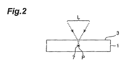
- Fig. 2 is a sectional view of the object 1 taken along the line II-II of Fig. 1
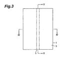
- Fig. 3 is a plan view of the object 1 after laser processing
- Fig. 4 is a sectional view of the object 1 taken along the line IV-IV of Fig. 3
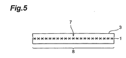
- Fig. 5 is a sectional view of the object 1 taken along the line V-V of Fig. 3
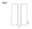
- Fig. 6 is a plan view of the cut object 1.
- the front face 3 of the object 1 has a desirable line along which the object should be cut 5 for cutting the object 1.
- the line along which the object should be cut 5 is a linearly extending virtual line (the object 1 may also be formed with an actual line acting as the line along which the object should be cut 5).
- the object 1 is irradiated with laser light L such that a light-converging point P is positioned within the object 1 under a condition causing multiphoton absorption, so as to form a modified region 7.
- the light-converging point is a location where the laser light L is converged.
- the laser light L is relatively moved along the line along which the object should be cut 5 (in the direction of arrow A), so as to move the light-converging point P along the line along which the object should be cut 5.
- This forms the modified region 7 along the line along which the object should be cut 5 only within the object 1 as shown in Figs. 3 to 5, and the modified region 7 forms a starting point region for cutting (part to cut) 8.
- no modified region 7 is formed upon heating the object 1 by causing the object 1 to absorb the laser light L.
- the laser light L is transmitted through the object 1, so as to generate multiphoton absorption within the object 1, thereby forming the modified region 7.
- the laser light L is hardly absorbed by the front face 3 of the object 1, whereby the front face 3 of the object 1 does not melt.
- the first case is where, after forming the starting point region for cutting, an artificial force is applied to the object, so that the object fractures from the starting point region for cutting acting as a start point, whereby the object is cut.
- This is the cutting in the case where the object has a large thickness, for example.
- the application of an artificial force encompasses application of bending stress and shearing stress along the starting point region for cutting of the object, and exertion of a temperature difference upon the object to generate thermal stress, for example.
- the other case is where a starting point region for cutting is formed, so that the object is naturally fractured in a cross-sectional direction (thickness direction) of the object from the starting point region for cutting acting as a start point, whereby the object is cut.
- This is enabled, for example, by forming the starting point region for cutting by a single row of modified regions when the object has a small thickness, and by a plurality of rows of modified regions aligned in the thickness direction when the object has a large thickness.
- fractures do not extend to the front face at a location not formed with the starting point region for cutting in the part to cut, whereby only the part corresponding to the location formed with the starting point region for cutting can be fractured.
- fracturing can be regulated well.
- Such a fracturing method with favorable controllability is quite effective, since objects to be processed such as silicon wafers have recently been apt to become thinner.
- the modified region formed by multiphoton absorption in this embodiment includes the following cases (1) to (3):
- An object to be processed e.g., glass
- a light-converging point is positioned therewithin under a condition with an electric field intensity of at least 1 ⁇ 10 8 (W/cm 2 ) at the light-converging point and a pulse width of 1 ns or less.
- an electric field intensity of at least 1 ⁇ 10 8 (W/cm 2 ) at the light-converging point and a pulse width of 1 ns or less.
- the pulse width is preferably 1 ns or less, more preferably 1 ps or less, for example.
- the forming of a refractive index change region by multiphoton absorption is described, for example, in "Formation of Photoinduced Structure within Glass by Femtosecond Laser Irradiation", Proceedings of 42th Laser Materials Processing Conference (November 1997), pp. 105-111.
- the starting point region for cutting is preferably formed in a direction along the (111) plane (first cleavage plane) or (110) plane (second cleavage plane).
- the starting point region for cutting is preferably formed in a direction along the (110) plane.
- a starting point region for cutting is preferably formed in a direction along the (1120) plane (A plane) or (1100) plane (M plane) while using the (0001) plane (C plane) as a principal plane.
- the starting point region for cutting extending along the direction to be formed with the starting point region for cutting can be formed in the substrate in an easy and accurate manner with reference to the orientation flat.
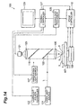
- Fig. 14 is a schematic diagram of the laser processing apparatus 100.
- the laser processing apparatus 100 comprises a laser light source 101 for generating laser light L; a laser light source controller 102 for controlling the laser light source 101 so as to regulate the output, pulse width, etc. of laser light L and the like; a dichroic mirror 103, arranged so as to change the orientation of the optical axis of laser light L by 90°, having a function of reflecting the laser light L; a light-converging lens 105 for converging the laser light L reflected by the dichroic mirror 103; a mounting table 107 for mounting an object to be processed 1 irradiated with the laser light L converged by the light-converging lens 105; an X-axis stage 109 for moving the mounting table 107 in the X-axis direction; a Y-axis stage 111 for moving the mounting table 107 in the Y-axis direction orthogonal to the X-axis direction; a Z-axis stage 113 for moving the mounting table 107 in the Z-axis direction orthogonal to the
- This movement of light-converging point P in X(Y)-axis direction is effected by moving the object 1 in the X(Y)-axis direction by the X(Y)-axis stage 109 (111).
- the Z-axis direction is a direction orthogonal to the front face 3 of the object 1, and thus becomes the direction of focal depth of laser light L incident on the object 1. Therefore, moving the Z-axis stage 113 in the Z-axis direction can position the light-converging point P of laser light L within the object 1. This can place the light-converging point P at a desirable position such as the substrate, the laminate part on the substrate, or the like in the object 1 when the object 1 has a multilayer structure, for example.
- the laser light source 101 is an Nd:YAG laser generating pulse laser light.
- Known as other kinds of laser usable as the laser light source 101 include Nd:YVO 4 laser, Nd:YLF laser, and titanium sapphire laser.
- pulse laser light is used for processing the object 1 in this embodiment, continuous wave laser light may be used as long as it can cause multiphoton absorption.
- the laser processing apparatus 100 further comprises an observation light source 117 for generating a visible light beam for irradiating the object 1 mounted on the mounting table 107, and a visible light beam splitter 119 disposed on the same optical axis as that of the dichroic mirror 103 and light-converging lens 105.
- the dichroic mirror 103 is disposed between the beam splitter 119 and light-converging lens 105.
- the beam splitter 119 has a function of reflecting about a half of a visual light beam and transmitting the remaining half therethrough, and is arranged so as to change the orientation of the optical axis of the visual light beam by 90°.
- the laser processing apparatus 100 further comprises an image pickup device 121 and an imaging lens 123 which are disposed on the same optical axis as that of the beam splitter 119, dichroic mirror 103, and light-converging lens 105.
- An example of the image pickup device 121 is a CCD camera.
- the reflected light of the visual light beam having illuminated the front face 3 including the line along which the object should be cut 5 and the like is transmitted through the light-converging lens 105, dichroic mirror 103, and beam splitter 119 and forms an image by way of the imaging lens 123, whereas thus formed image is captured by the image pickup device 121, so as to yield imaging data.
- the laser processing apparatus 100 further comprises an imaging data processor 125 for inputting the imaging data outputted from the image pickup device 121, an overall controller 127 for controlling the laser processing apparatus 100 as a whole, and a monitor 129.
- the imaging data processor 125 calculates focal point data for positioning the focal point of the visible light generated from the observation light source 117 onto the front face 3 of the object 1.
- the stage controller 115 controls the movement of the Z-axis stage 113, so that the focal point of visible light is positioned on the front face 3 of the object.
- the imaging data processor 125 functions as an autofocus unit.
- the imaging data processor 125 calculates image data such as an enlarged image of the front face 3.
- the image data is sent to the overall controller 127, subjected to various kinds of processing therein, and then sent to the monitor 129. As a consequence, an enlarged image or the like is displayed on the monitor 129.
- the overall controller 127 regulates the laser light source controller 102, observation light source 117, and stage controller 115, thereby controlling the laser processing apparatus 100 as a whole.
- the overall controller 127 functions as a computer unit.
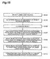
- Fig. 15 is a flowchart for explaining the starting point region for cutting forming step.
- Light absorption characteristics of the substrate of the object 1 are determined by a spectrophotometer or the like which is not depicted. According to the results of measurement, a laser light source 101 generating laser light L having a wavelength to which the substrate of the object 1 is transparent or exhibits a low absorption is chosen (S101). Subsequently, in view of the thickness and refractive index of the object 1, the amount of movement of the object 1 in the Z-axis direction in the laser processing apparatus 100 is determined (S103).
- This amount of movement is fed into the overall controller 127.
- the object 1 is mounted on the mounting table 107 of the laser processing apparatus 100 such that the rear face of the substrate faces the light-converging lens 105. Subsequently, the thickness of the object 1 is measured. According to the result of measurement of thickness and the refractive index of the object 1, the amount of movement of the object 1 in the Z-axis direction is determined (S103). This is an amount of movement of the object 1 in the Z-axis direction with reference to the light-converging point of laser light L positioned at the front face 3 of the object 1 in order for the light-converging point P of laser light L to be positioned within the object 1. This amount of movement is fed into the overall controller 127.
- the object 1 is mounted on the mounting table 107 of the laser processing apparatus 100. Subsequently, visible light is generated from the observation light source 117, so as to illuminate the front face of the object 1 (S105). The illuminated front face 3 of the object 1 including the line along which the object should be cut 5 is captured by the image pickup device 121. The imaging data captured by the imaging device 121 is sent to the imaging data processor 125. According to the imaging data, the imaging data processor 125 calculates such focal point data that the focal point of visible light from the observation light source 117 is positioned at the front face 3 (S107).
- the focal point data is sent to the stage controller 115.
- the stage controller 115 moves the Z-axis stage 113 in the Z-axis direction (S109).
- the focal point of visible light from the observation light source 117 is positioned at the front face 3 of the object 1.
- the imaging data processor 125 calculates enlarged image data of the front face 3 of the object 1 including the line along which the object should be cut 5.
- the enlarged image data is sent to the monitor 129 by way of the overall controller 127, whereby an enlarged image of the line along which the object should be cut 5 and its vicinity is displayed on the monitor 129.
- Movement amount data determined in step S103 has been fed into the overall controller 127 beforehand, and is sent to the stage controller 115.
- the stage controller 115 causes the Z-axis stage 113 to move the object 1 in the Z-axis direction to a position where the light-converging point P of laser light L is positioned within the object 1 (S111).
- laser light L is generated from the laser light source 101, so as to irradiate the line along which the object should be cut 5 in the front face 3 of the substrate of the object 1. Since the light-converging point P of the laser light L is positioned within the object 1, a modified region is formed only within the object 1. Then, the X-axis stage 109 and Y-axis stage 111 are moved along the line along which the object should be cut 5, such that the modified region formed along the line along which the object should be cut 5 forms a starting point region for cutting within the object 1 along the line along which the object should be cut 5 (S113).
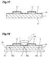
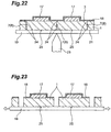
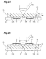
- Figs. 17, 18, and 22 to 24 are partial sectional views of the object to be processed 1 taken along the line XVII-XVII of Fig. 16.
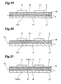
- Figs. 19 to 21 are partial sectional views of the object 1 taken along the line XIX-XIX of Fig. 16.
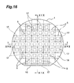
- the front face 3 of the object to be processed 1 which is a silicon wafer, is formed with a plurality of functional devices 17 in a matrix in parallel with an orientation flat 16 of the object 1, whereby the object 1 is produced.
- an insulating film 18 made of SiO 2 or the like, which covers the front face 3 and functional devices 17.
- the object 1 is a substrate, whereas Lhe functional devices 1/ and insulating film 18 constitute a laminate part disposed on the front face of the substrate.
- the laminate part disposed on the front face of the substrate refers to one deposited on the front face of the substrate, one bonded onto the front face of the substrate, one attached to the front face of the substrate, etc., regardless of whether its material is different from or identical to that of the substrate.
- the laminate part disposed on the front face of the substrate includes one disposed in close contact with the substrate, one disposed with a gap from the substrate, etc.
- the laminate part examples include semiconductor active layers formed by crystal growth on the substrate, functional devices (which refer to light-receiving devices such as photodiodes and light-emitting devices such as laser diodes, circuit devices formed as a circuit, etc.) formed on the substrate, glass substrates bonded onto other glass substrates, etc.
- the laminate part also includes one in which a plurality of layers are formed from materials different from each other.
- an expandable expansion film 19 is attached to the rear face 21 of the object 1, and then the object 1 is mounted on the mounting table 107 of the above-mentioned laser processing apparatus 100, for example, such that the front face 3 side of the object 1 faces the light-converging lens 105.
- the object 1 is irradiated with laser light L while its light-converging point P is positioned within the object 1, so as to form a modified region 7 within the object 1, and cause the modified region 7 to form a starting point region for cutting 8 along a line along which the object should be cut 5 inside by a predetermined distance from the front face 3 (laser light incident face) of the object 1 (starting point region for cutting forming step). Since the object to be processed 1 is a silicon wafer, a molten processed region is formed as the modified region 7.
- the starting point region for cutting 8 deviated from a center line L passing the center position of the object 1 in the thickness direction toward the front face (one end face) 3 is formed along the line along which the object should be cut 5.
- the width in the thickness direction (hereinafter simply be referred to as "width") of an unmodified region la positioned on the front face 3 side of the starting point region for cutting 8 is 20 ⁇ m
- the width of the starting point region for cutting 8 i.e.,modified region 7
- the width of an unmodified region 1b positioned on the rear face 21 side of the starting point region for cutting 8 is 40 ⁇ m.
- the width of the unmodified region 1a is 10 ⁇ m
- the width of the starting point region for cutting 8 is 20 ⁇ m
- the width of the unmodified region 1b is 20 ⁇ m.
- a mode of “the starting point region for cutting 8 deviated from the center line CL toward the front face 3” include the following two cases, for example. Namely, there are “a case where the whole starting point region for cutting 8 is positioned on the front face 3 side of the center line CL” as shown in Fig. 20, and “a case where two starting point regions for cutting 8a, 8b are formed on the front face 3 side and the rear face 21 side, such that the starting point region for cutting 8b on the rear face 21 side is positioned on the center line CL, whereas the starting point region for cutting 8a on the front face 3 side is positioned between the starting point region for cutting 8b and the front face 3".
- the thickness of the object 1 is 100 ⁇ m
- the width of the unmodified region 1a is 30 ⁇ m
- the width of the starting point region for cutting 8 is 10 ⁇ m
- the width of the unmodified region 1b is 60 ⁇ m.
- the thickness of the object 1 is 200 ⁇ m
- the width of the unmodified region 1a is 20 ⁇ m
- the width of the starting point region for cutting 8a is 40 ⁇ m
- the width of the unmodified region 1c positioned between the starting point regions for cutting 8a, 8b is 20 ⁇ m
- the width of the starting point region for cutting 8b is 40 ⁇ m
- the width of the unmodified region 1b is 80 ⁇ m.
- the line along which the object should be cut 5 is scanned with the laser light L.
- the line along which the object should be cut 5 is set like a grid passing between functional devices 17, 17 adjacent each other (see Fig. 16).
- the positional data of the line along which the object should be cut 5 with respect to the object 1 is stored into a storage section in the overall controller 127 in the laser processing apparatus 100, for example.
- a knife edge 23 as pressing means is pressed against the object 1 from the rear face (other end face) 21 side thereof by way of the expansion film 19, so as to generate a fracture 24 from the starting point region for cutting 8 acting as a start point, and cause the fracture 24 to reach the front face 3 and rear face 21 of the object 1 (pressing step).
- the object 1 is divided into individual semiconductor chips 25 each having one functional device 17.
- the positional data of the line along which the object should be cut 5 stored in the storage section is read out, and the knife edge 23 is controlled according to the positional data, so as to be pressed against the object 1 along the line along which the object should be cut 5, whereby the object 1 is pressed along the line along which the object should be cut 5.
- the positional data of the line along which the object should be cut with respect to the object 1 is stored in the starting point region for cutting forming step, and the object 1 is pressed against the line along which the object should be cut 5 according to the positional data in the pressing step, whereby the pressing force can act easily and accurately on the starting point region for cutting 8 formed within the substrate 1. Then, pressing the object 1 along the line along which the object should be cut 5 can accurately cut the object 1 into each functional device 17 while substantially eliminating the action of the pressing force on the functional devices 17.
- the knife edge 23 is pressed against the rear face 21 of the object 1 along the starting point region for cutting (part to cut) 8 formed by the modified region 7, so as to break and cut the object 1. This is because a large tensile stress among bending stresses generated upon pressing the knife edge 23 acts on the modified region 7, whereby the object 1 can be cut with a relatively small force.
- the expansion film 19 is expanded outward, so as to separate the semiconductor chips 25 from each other as shown in Fig. 23. Separating the semiconductor chips 25 from each other by using the expansion film 19 as such can make it easier to pick up the semiconductor chips 25.
- the modified region 7 formed by multiphoton absorption forms the region to cut 8 within the object 1 along the line along which the object should be cut 5.
- the multiphoton absorption occurs locally within the object 1, so that the laser light L is hardly absorbed by the front face 3 and rear face 21 of the object 1, whereby the front face 3 and rear face 21 can be prevented from melting upon irradiation with the laser light L.
- the region to cut 8 is formed so as to shift from the center line CL of the object 1 toward the front face 3, when the object 1 is pressed by the knife edge 23 from the rear face 21 side, the fracture can be generated in the object 1 from the starting point region for cutting 8 acting as a start point by a smaller pressing force than in the case where the starting point region for cutting 8 is formed on the center line CL. This can accurately cut the object 1 along the line along which the object should be cut 5 while preventing unnecessary fractures deviating from the line along which the object should be cut 5 from occurring.
- the starting point region for cutting 8 can be formed as follows. Namely, as shown in Fig. 24, a protection film 20 for protecting the functional devices 17 is attached to the front face 3 side of the object 1 before attaching the expansion film 19, and the object 1 is mounted on the mounting table 107 of the above-mentioned laser processing apparatus 100, for example, such that the rear face 21 side of the object 1 faces the light-converging lens 105.
- the object 1 is irradiated with the laser light L while the light-converging point P is positioned therewithin, so as to form a modified region 7 within the object 1, and cause the modified region 7 to form a starting point region for cutting 8 shifted from the center line CL to the front face 3 side of the object 1 along the line along which the object should be cut 5.
- FIGs. 25 to 27 are partial sectional views of the object 1 taken along the line XVII-XVII of Fig. 16.
- the object to be processed 1 shown in Figs. 16 and 17 is produced, and a starting point region for cutting 8 is formed along a line along which the object should be cut 5 inside by a predetermined distance from the front face 3 (laser light incident face) of the object 1 (starting point region for cutting forming step).
- the starting point region for cutting forming step in Example 2 the starting point region for cutting 8 shifted from the center line CL passing the center position of the object 1 in the thickness direction toward the rear face (one end face) 21 is formed along the line along which the object should be cut 5 as shown in Fig. 25.
- a protective film 20 is attached to the front face 3 side of the object to be processed 1, so as to cover the functional devices 17.
- the knife edge 23 is pressed against the object 1 from the front face (other face) 3 side of the object 1 by way of the expansion film 19, so as to generate a fracture 24 from the starting point region for cutting 8 acting as a start point, and cause the fracture 24 to reach the front face 3 and rear face 21 of the object 1 (pressing step).
- the object 1 is divided into individual semiconductor chips 25 each having one functional device 17.
- the positional data of the line along which the object should be cut 5 stored in the storage section is read out, and the knife edge 23 is controlled according to the positional data, so as to be pressed against the object 1 along the line along which the object should be cut 5, whereby the object 1 is pressed along the line along which the object should be cut 5.
- the knife edge 23 is pressed against the front face 3 of the object 1 along the starting point region for cutting (part to cut) 8 formed by the modified region 7, so as to break and cut the object 1. This is because a large tensile stress among bending stresses generated upon pressing the knife edge 23 acts on the modified region 7, whereby the object 1 can be cut with a relatively small force.
- the protective film 20 is peeled off from the object 1, and the expansion film 19 is expanded outward, so as to separate the semiconductor chips 25 from each other as in Example 1, whereby the semiconductor chips 25 are picked up.
- the starting point region for cutting 8 is formed so as to shift from the center line CL of the object 1 toward the rear face 21. Therefore, when the knife edge 23 presses the object 1 from the front face 3 side, the fracture 24 can be generated in the object 1 from the starting point region for cutting 8 acting as a start point by a smaller pressing force than in the case where the starting point region for cutting 8 is formed on the center line CL. This can accurately cut the object 1 along the line along which the object should be cut 5 while preventing unnecessary fractures deviating from the line along which the object should be cut 5 from occurring. Also, since the object 1 can be cut with a small pressing force, the influence on the functional devices 17 when the object 1 is pressed from the front face 3 side can be alleviated.
- the object 1 is irradiated with the laser light L while the light-converging point P is positioned therewithin, so as to form a modified region 7 within the object 1, and cause the modified region 7 to form a starting point region for cutting 8 shifted from the center line CL toward the rear face 21 of the object 1 along the line along which the object should be cut 5 by a method similar to that of Example 1 mentioned above as shown in Fig. 27.
- the present invention is not limited to the above-mentioned embodiment.
- the object 1 as a whole on the front face 3 side or rear face 21 side may be pressed with a roller or the like. Since the fracture 24 is generated from the starting point region for cutting 8 acting as a start point, the object 1 can efficiently be cut along the line along which the object should be cut 5 in this case as well.
- parts (e.g., respective parts of the functional devices 17) of the object 1 on the front face 3 side or rear face 21 side may successively be pressed with a pressure needle or the like.
- Means for pressing the object 1 along the line along which the object should be cut 5 includes not only the above-mentioned knife edge 23, but also a cutter.
- the method of cutting an object to be processed in accordance with the present invention can accurately cut the object to be processed.
Landscapes
- Engineering & Computer Science (AREA)
- Chemical & Material Sciences (AREA)
- Mechanical Engineering (AREA)
- Organic Chemistry (AREA)
- Physics & Mathematics (AREA)
- Materials Engineering (AREA)
- Optics & Photonics (AREA)
- Plasma & Fusion (AREA)
- General Chemical & Material Sciences (AREA)
- Oil, Petroleum & Natural Gas (AREA)
- Chemical Kinetics & Catalysis (AREA)
- Mining & Mineral Resources (AREA)
- Laser Beam Processing (AREA)
- Dicing (AREA)
- Processing Of Stones Or Stones Resemblance Materials (AREA)
- Re-Forming, After-Treatment, Cutting And Transporting Of Glass Products (AREA)
- Led Devices (AREA)
- Finish Polishing, Edge Sharpening, And Grinding By Specific Grinding Devices (AREA)
- Semiconductor Lasers (AREA)
Abstract
Description
Claims (3)
- A method of cutting an object to be processed, the method comprising:a starting point region for cutting forming step of irradiating a wafer-like object to be processed with laser light while positioning a light-converging point therewithin, so as to form a modified region due to multiphoton absorption within the object, and causing the modified region to form a starting point region for cutting, deviated from a center position of the object in a thickness direction thereof toward one end face of the object, along a line along which the object should be cut in the object; anda pressing step of pressing the object from the other end face side of the object.
- A method of cutting an object to be processed according to claim 1, wherein the object is pressed along the line along which the object should be cut in the pressing step.
- A method of cutting an object to be processed according to claim 2, wherein positional data of the line along which the object should be cut with respect to the object is stored in the starting point region for cutting forming step; and
wherein the object is pressed along the line along which the object should be cut according to the positional data in the pressing step.
Priority Applications (2)
| Application Number | Priority Date | Filing Date | Title |
|---|---|---|---|
| EP10005696.9A EP2216128B1 (en) | 2002-03-12 | 2003-03-11 | Method of cutting object to be processed |
| EP10189319.6A EP2272618B1 (en) | 2002-03-12 | 2003-03-11 | Method of cutting object to be processed |
Applications Claiming Priority (3)
| Application Number | Priority Date | Filing Date | Title |
|---|---|---|---|
| JP2002067372 | 2002-03-12 | ||
| JP2002067372 | 2002-03-12 | ||
| PCT/JP2003/002867 WO2003076119A1 (en) | 2002-03-12 | 2003-03-11 | Method of cutting processed object |
Related Child Applications (4)
| Application Number | Title | Priority Date | Filing Date |
|---|---|---|---|
| EP10005696.9A Division EP2216128B1 (en) | 2002-03-12 | 2003-03-11 | Method of cutting object to be processed |
| EP10189319.6A Division EP2272618B1 (en) | 2002-03-12 | 2003-03-11 | Method of cutting object to be processed |
| EP10005696.9 Division-Into | 2010-06-01 | ||
| EP10189319.6 Division-Into | 2010-10-28 |
Publications (3)
| Publication Number | Publication Date |
|---|---|
| EP1498216A1 true EP1498216A1 (en) | 2005-01-19 |
| EP1498216A4 EP1498216A4 (en) | 2009-07-01 |
| EP1498216B1 EP1498216B1 (en) | 2010-12-29 |
Family
ID=27800281
Family Applications (9)
| Application Number | Title | Priority Date | Filing Date |
|---|---|---|---|
| EP10189319.6A Expired - Lifetime EP2272618B1 (en) | 2002-03-12 | 2003-03-11 | Method of cutting object to be processed |
| EP10005696.9A Expired - Lifetime EP2216128B1 (en) | 2002-03-12 | 2003-03-11 | Method of cutting object to be processed |
| EP03744054A Expired - Lifetime EP1498216B1 (en) | 2002-03-12 | 2003-03-11 | Method of cutting processed object |
| EP15192444.6A Expired - Lifetime EP3020503B1 (en) | 2002-03-12 | 2003-03-12 | Laser processing method |
| EP19188428.7A Expired - Lifetime EP3683003B1 (en) | 2002-03-12 | 2003-03-12 | Laser processing method |
| EP10157594.2A Expired - Lifetime EP2199008B1 (en) | 2002-03-12 | 2003-03-12 | Laser processing method |
| EP10157597.5A Expired - Lifetime EP2199009B1 (en) | 2002-03-12 | 2003-03-12 | Laser Processing Method |
| EP03712675A Expired - Lifetime EP1498215B1 (en) | 2002-03-12 | 2003-03-12 | Laser processing method |
| EP15192453.7A Expired - Lifetime EP3012061B1 (en) | 2002-03-12 | 2003-03-12 | Laser processing method |
Family Applications Before (2)
| Application Number | Title | Priority Date | Filing Date |
|---|---|---|---|
| EP10189319.6A Expired - Lifetime EP2272618B1 (en) | 2002-03-12 | 2003-03-11 | Method of cutting object to be processed |
| EP10005696.9A Expired - Lifetime EP2216128B1 (en) | 2002-03-12 | 2003-03-11 | Method of cutting object to be processed |
Family Applications After (6)
| Application Number | Title | Priority Date | Filing Date |
|---|---|---|---|
| EP15192444.6A Expired - Lifetime EP3020503B1 (en) | 2002-03-12 | 2003-03-12 | Laser processing method |
| EP19188428.7A Expired - Lifetime EP3683003B1 (en) | 2002-03-12 | 2003-03-12 | Laser processing method |
| EP10157594.2A Expired - Lifetime EP2199008B1 (en) | 2002-03-12 | 2003-03-12 | Laser processing method |
| EP10157597.5A Expired - Lifetime EP2199009B1 (en) | 2002-03-12 | 2003-03-12 | Laser Processing Method |
| EP03712675A Expired - Lifetime EP1498215B1 (en) | 2002-03-12 | 2003-03-12 | Laser processing method |
| EP15192453.7A Expired - Lifetime EP3012061B1 (en) | 2002-03-12 | 2003-03-12 | Laser processing method |
Country Status (11)
| Country | Link |
|---|---|
| US (7) | US7749867B2 (en) |
| EP (9) | EP2272618B1 (en) |
| JP (9) | JP4606741B2 (en) |
| KR (3) | KR100749972B1 (en) |
| CN (3) | CN1328002C (en) |
| AT (2) | ATE493226T1 (en) |
| AU (2) | AU2003211581A1 (en) |
| DE (1) | DE60335538D1 (en) |
| ES (3) | ES2356817T3 (en) |
| TW (2) | TWI270431B (en) |
| WO (2) | WO2003076119A1 (en) |
Cited By (18)
| Publication number | Priority date | Publication date | Assignee | Title |
|---|---|---|---|---|
| WO2006051861A1 (en) | 2004-11-12 | 2006-05-18 | Hamamatsu Photonics K.K. | Laser processing method |
| EP1610364A4 (en) * | 2003-03-12 | 2008-08-27 | Hamamatsu Photonics Kk | Laser beam machining method |
| EP1742252A4 (en) * | 2004-03-30 | 2009-01-14 | Hamamatsu Photonics Kk | LASER PROCESSING PROCESS AND OBJECT TO BE PROCESSED |
| EP1906438A4 (en) * | 2005-07-04 | 2009-04-22 | Hamamatsu Photonics Kk | METHOD OF CUTTING PIECE |
| EP1983557A4 (en) * | 2005-12-27 | 2009-04-22 | Hamamatsu Photonics Kk | LASER BEAM MACHINING PROCESS AND SEMICONDUCTOR CHIP |
| US7547613B2 (en) | 2000-09-13 | 2009-06-16 | Hamamatsu Photonics K.K. | Laser processing method and laser processing apparatus |
| US7566635B2 (en) | 2002-03-12 | 2009-07-28 | Hamamatsu Photonics K.K. | Substrate dividing method |
| US7749867B2 (en) | 2002-03-12 | 2010-07-06 | Hamamatsu Photonics K.K. | Method of cutting processed object |
| CN101875156A (en) * | 2009-04-30 | 2010-11-03 | 三星钻石工业股份有限公司 | Laser machining method and laser machining apparatus |
| EP2340911A1 (en) * | 2009-12-25 | 2011-07-06 | Mitsuboshi Diamond Industrial Co., Ltd. | Laser processing method of a workpiece by forming division originating points inthere, dividing method for a workpiece, and laser processing apparatus |
| WO2011104097A1 (en) * | 2010-02-24 | 2011-09-01 | Osram Opto Semiconductors Gmbh | Method for producing a plurality of optoelectronic semiconductor chips |
| EP1742253B1 (en) * | 2004-03-30 | 2012-05-09 | Hamamatsu Photonics K.K. | Laser processing method |
| EP2471627A1 (en) * | 2010-12-29 | 2012-07-04 | Blösch Ressourcen AG | Method for producing mechanical workpieces from a board of monocrystalline silicon |
| DE102006053958B4 (en) * | 2005-11-16 | 2012-08-30 | Denso Corporation | A compound method for a semiconductor substrate and a layer, and semiconductor chip manufacturing method using the same |
| US8450187B2 (en) | 2002-12-03 | 2013-05-28 | Hamamatsu Photonics K.K. | Method of cutting semiconductor substrate |
| WO2013184740A1 (en) * | 2012-06-05 | 2013-12-12 | Corning Incorporated | Methods of cutting glass using a laser |
| WO2015052217A1 (en) * | 2013-10-08 | 2015-04-16 | Siltectra Gmbh | Method for manufacturing solid state elements by a laser treatment and temperature-induced stresses |
| CN110931427A (en) * | 2018-09-20 | 2020-03-27 | 三星电子株式会社 | Method for manufacturing a semiconductor device |
Families Citing this family (239)
| Publication number | Priority date | Publication date | Assignee | Title |
|---|---|---|---|---|
| FR2852250B1 (en) | 2003-03-11 | 2009-07-24 | Jean Luc Jouvin | PROTECTIVE SHEATH FOR CANNULA, AN INJECTION KIT COMPRISING SUCH ANKLE AND NEEDLE EQUIPPED WITH SUCH ANKLE |
| DE60315515T2 (en) | 2003-03-12 | 2007-12-13 | Hamamatsu Photonics K.K., Hamamatsu | LASER PROCESSING PROCEDURES |
| KR101169182B1 (en) * | 2003-06-06 | 2012-07-30 | 히다치 가세고교 가부시끼가이샤 | Semiconductor device producing method |
| JP2005032903A (en) | 2003-07-10 | 2005-02-03 | Oki Electric Ind Co Ltd | Semiconductor device and manufacturing method thereof |
| WO2005007335A1 (en) * | 2003-07-18 | 2005-01-27 | Hamamatsu Photonics K.K. | Laser processing method and device, and processed product |
| JP4563097B2 (en) | 2003-09-10 | 2010-10-13 | 浜松ホトニクス株式会社 | Semiconductor substrate cutting method |
| JP2005101413A (en) * | 2003-09-26 | 2005-04-14 | Disco Abrasive Syst Ltd | Method and apparatus for dividing thin plate workpiece |
| JP4175636B2 (en) | 2003-10-31 | 2008-11-05 | 株式会社日本製鋼所 | Glass cutting method |
| JP4569097B2 (en) * | 2003-11-18 | 2010-10-27 | 凸版印刷株式会社 | Spherical surface acoustic wave device and manufacturing method thereof |
| JP4509578B2 (en) * | 2004-01-09 | 2010-07-21 | 浜松ホトニクス株式会社 | Laser processing method and laser processing apparatus |
| JP4601965B2 (en) * | 2004-01-09 | 2010-12-22 | 浜松ホトニクス株式会社 | Laser processing method and laser processing apparatus |
| JP4598407B2 (en) * | 2004-01-09 | 2010-12-15 | 浜松ホトニクス株式会社 | Laser processing method and laser processing apparatus |
| JP2005268752A (en) | 2004-02-19 | 2005-09-29 | Canon Inc | Laser cleaving method, member to be cleaved, and semiconductor element chip |
| CN1938827B (en) * | 2004-03-30 | 2010-05-26 | 浜松光子学株式会社 | Laser processing method and semiconductor chip |
| US7491288B2 (en) * | 2004-06-07 | 2009-02-17 | Fujitsu Limited | Method of cutting laminate with laser and laminate |
| JP4938998B2 (en) * | 2004-06-07 | 2012-05-23 | 富士通株式会社 | Substrate and laminate cutting method, and laminate production method |
| JP2006040949A (en) * | 2004-07-22 | 2006-02-09 | Advanced Lcd Technologies Development Center Co Ltd | Laser crystallization apparatus and laser crystallization method |
| WO2006013763A1 (en) * | 2004-08-06 | 2006-02-09 | Hamamatsu Photonics K.K. | Laser processing method and semiconductor device |
| KR100628276B1 (en) * | 2004-11-05 | 2006-09-27 | 엘지.필립스 엘시디 주식회사 | Scribing equipment and substrate cutting device having same and substrate cutting method using same |
| JP4917257B2 (en) * | 2004-11-12 | 2012-04-18 | 浜松ホトニクス株式会社 | Laser processing method |
| JP2006173428A (en) * | 2004-12-17 | 2006-06-29 | Seiko Epson Corp | Substrate processing method and element manufacturing method |
| JP4809632B2 (en) * | 2005-06-01 | 2011-11-09 | ルネサスエレクトロニクス株式会社 | Manufacturing method of semiconductor device |
| JP4938261B2 (en) * | 2005-08-11 | 2012-05-23 | 株式会社ディスコ | Laser processing method for liquid crystal device wafer |
| JP4742751B2 (en) * | 2005-08-30 | 2011-08-10 | セイコーエプソン株式会社 | Display panel, laser scribing method for display panel, and electronic device |
| JP4762653B2 (en) * | 2005-09-16 | 2011-08-31 | 浜松ホトニクス株式会社 | Laser processing method and laser processing apparatus |
| JP2007095952A (en) * | 2005-09-28 | 2007-04-12 | Tokyo Seimitsu Co Ltd | Laser dicing apparatus and laser dicing method |
| US7687322B1 (en) * | 2005-10-11 | 2010-03-30 | SemiLEDs Optoelectronics Co., Ltd. | Method for removing semiconductor street material |
| WO2007055010A1 (en) | 2005-11-10 | 2007-05-18 | Renesas Technology Corp. | Semiconductor device manufacturing method and semiconductor device |
| US7838331B2 (en) * | 2005-11-16 | 2010-11-23 | Denso Corporation | Method for dicing semiconductor substrate |
| US7662668B2 (en) * | 2005-11-16 | 2010-02-16 | Denso Corporation | Method for separating a semiconductor substrate into a plurality of chips along with a cutting line on the semiconductor substrate |
| US20070111480A1 (en) * | 2005-11-16 | 2007-05-17 | Denso Corporation | Wafer product and processing method therefor |
| JP4923874B2 (en) * | 2005-11-16 | 2012-04-25 | 株式会社デンソー | Semiconductor wafer |
| JP2007165851A (en) * | 2005-11-16 | 2007-06-28 | Denso Corp | Dicing seat frame |
| JP4872503B2 (en) * | 2005-11-16 | 2012-02-08 | 株式会社デンソー | Wafer and wafer processing method |
| JP2007142000A (en) * | 2005-11-16 | 2007-06-07 | Denso Corp | Laser processing apparatus and laser processing method |
| KR100858983B1 (en) * | 2005-11-16 | 2008-09-17 | 가부시키가이샤 덴소 | Semiconductor device and dicing method for semiconductor substrate |
| JP2007165850A (en) * | 2005-11-16 | 2007-06-28 | Denso Corp | Wafer and wafer cutting method |
| JP4736738B2 (en) * | 2005-11-17 | 2011-07-27 | 株式会社デンソー | Laser dicing method and laser dicing apparatus |
| JP4907965B2 (en) * | 2005-11-25 | 2012-04-04 | 浜松ホトニクス株式会社 | Laser processing method |
| JP2007165706A (en) * | 2005-12-15 | 2007-06-28 | Renesas Technology Corp | Manufacturing method of semiconductor integrated circuit device |
| JP4655915B2 (en) * | 2005-12-15 | 2011-03-23 | セイコーエプソン株式会社 | Method for dividing layered substrate |
| JP4804911B2 (en) * | 2005-12-22 | 2011-11-02 | 浜松ホトニクス株式会社 | Laser processing equipment |
| US7960202B2 (en) * | 2006-01-18 | 2011-06-14 | Hamamatsu Photonics K.K. | Photodiode array having semiconductor substrate and crystal fused regions and method for making thereof |
| GB2434767A (en) * | 2006-02-02 | 2007-08-08 | Xsil Technology Ltd | Laser machining |
| US20070181545A1 (en) * | 2006-02-06 | 2007-08-09 | Boyette James E | Method and apparatus for controlling sample position during material removal or addition |
| JP2007235008A (en) * | 2006-03-03 | 2007-09-13 | Denso Corp | Wafer cutting method and chip |
| JP4322881B2 (en) * | 2006-03-14 | 2009-09-02 | 浜松ホトニクス株式会社 | Laser processing method and laser processing apparatus |
| JP2007290304A (en) * | 2006-04-27 | 2007-11-08 | Casio Comput Co Ltd | Brittle sheet material cutting method and apparatus |
| JP2007304296A (en) * | 2006-05-11 | 2007-11-22 | Sony Corp | Liquid crystal display device, manufacturing method thereof, and video display device |
| JP2007304297A (en) * | 2006-05-11 | 2007-11-22 | Sony Corp | Manufacturing method of liquid crystal display device |
| US20070298529A1 (en) * | 2006-05-31 | 2007-12-27 | Toyoda Gosei, Co., Ltd. | Semiconductor light-emitting device and method for separating semiconductor light-emitting devices |
| JP4480728B2 (en) * | 2006-06-09 | 2010-06-16 | パナソニック株式会社 | Method for manufacturing MEMS microphone |
| JP5183892B2 (en) | 2006-07-03 | 2013-04-17 | 浜松ホトニクス株式会社 | Laser processing method |
| ES2428826T3 (en) | 2006-07-03 | 2013-11-11 | Hamamatsu Photonics K.K. | Laser and chip processing procedure |
| JP4954653B2 (en) | 2006-09-19 | 2012-06-20 | 浜松ホトニクス株式会社 | Laser processing method |
| CN101516566B (en) * | 2006-09-19 | 2012-05-09 | 浜松光子学株式会社 | Laser processing method and laser processing apparatus |
| JP5101073B2 (en) * | 2006-10-02 | 2012-12-19 | 浜松ホトニクス株式会社 | Laser processing equipment |
| JP5132911B2 (en) * | 2006-10-03 | 2013-01-30 | 浜松ホトニクス株式会社 | Laser processing method |
| JP4964554B2 (en) * | 2006-10-03 | 2012-07-04 | 浜松ホトニクス株式会社 | Laser processing method |
| KR101428824B1 (en) * | 2006-10-04 | 2014-08-11 | 하마마츠 포토닉스 가부시키가이샤 | Laser processing method |
| US7892891B2 (en) * | 2006-10-11 | 2011-02-22 | SemiLEDs Optoelectronics Co., Ltd. | Die separation |
| GB0622232D0 (en) | 2006-11-08 | 2006-12-20 | Rumsby Philip T | Method and apparatus for laser beam alignment for solar panel scribing |
| KR20080075398A (en) * | 2007-02-12 | 2008-08-18 | 주식회사 토비스 | Cutting method of large TFT-LC panel |
| DE202007004412U1 (en) * | 2007-03-22 | 2008-07-24 | STABILA Messgeräte Gustav Ullrich GmbH | spirit level |
| US20080232419A1 (en) * | 2007-03-22 | 2008-09-25 | Seiko Epson Corporation | Laser array chip, laser module, manufacturing method for manufacturing laser module, manufacturing method for manufacturing laser light source, laser light source, illumination device, monitor, and projector |
| JP5336054B2 (en) * | 2007-07-18 | 2013-11-06 | 浜松ホトニクス株式会社 | Processing information supply system provided with processing information supply device |
| JP2009049390A (en) * | 2007-07-25 | 2009-03-05 | Rohm Co Ltd | Nitride semiconductor device and manufacturing method thereof |
| JP2009032970A (en) * | 2007-07-27 | 2009-02-12 | Rohm Co Ltd | Method of manufacturing nitride semiconductor device |
| JP4402708B2 (en) * | 2007-08-03 | 2010-01-20 | 浜松ホトニクス株式会社 | Laser processing method, laser processing apparatus and manufacturing method thereof |
| EP2178129B1 (en) * | 2007-08-03 | 2017-11-29 | Nichia Corporation | Method for manufacturing a gallium nitride compound semiconductor light emitting element |
| JP2009044600A (en) * | 2007-08-10 | 2009-02-26 | Panasonic Corp | Microphone device and manufacturing method thereof |
| JP5225639B2 (en) | 2007-09-06 | 2013-07-03 | 浜松ホトニクス株式会社 | Manufacturing method of semiconductor laser device |
| JP5449665B2 (en) * | 2007-10-30 | 2014-03-19 | 浜松ホトニクス株式会社 | Laser processing method |
| CN101939129A (en) * | 2007-11-07 | 2011-01-05 | 陶瓷技术股份公司 | Method for laser etching brittle components |
| JP5054496B2 (en) * | 2007-11-30 | 2012-10-24 | 浜松ホトニクス株式会社 | Processing object cutting method |
| JP5134928B2 (en) * | 2007-11-30 | 2013-01-30 | 浜松ホトニクス株式会社 | Workpiece grinding method |
| JP2010021398A (en) * | 2008-07-11 | 2010-01-28 | Disco Abrasive Syst Ltd | Method of treating wafer |
| KR100993088B1 (en) * | 2008-07-22 | 2010-11-08 | 엘지이노텍 주식회사 | Semiconductor light emitting device and manufacturing method thereof |
| JP5692969B2 (en) | 2008-09-01 | 2015-04-01 | 浜松ホトニクス株式会社 | Aberration correction method, laser processing method using this aberration correction method, laser irradiation method using this aberration correction method, aberration correction apparatus, and aberration correction program |
| US8051679B2 (en) * | 2008-09-29 | 2011-11-08 | Corning Incorporated | Laser separation of glass sheets |
| TWI419203B (en) * | 2008-10-16 | 2013-12-11 | 勝高股份有限公司 | Epitaxial substrate for solid-state imaging element with adsorption groove, semiconductor device, back-illuminated solid-state imaging element, and manufacturing method thereof |
| JP5254761B2 (en) | 2008-11-28 | 2013-08-07 | 浜松ホトニクス株式会社 | Laser processing equipment |
| JP5241525B2 (en) | 2009-01-09 | 2013-07-17 | 浜松ホトニクス株式会社 | Laser processing equipment |
| JP5241527B2 (en) | 2009-01-09 | 2013-07-17 | 浜松ホトニクス株式会社 | Laser processing equipment |
| JP2010177277A (en) * | 2009-01-27 | 2010-08-12 | Tokyo Seimitsu Co Ltd | Laser dicing method and laser dicing device |
| KR101757937B1 (en) | 2009-02-09 | 2017-07-13 | 하마마츠 포토닉스 가부시키가이샤 | Workpiece cutting method |
| US8347651B2 (en) * | 2009-02-19 | 2013-01-08 | Corning Incorporated | Method of separating strengthened glass |
| US8728916B2 (en) | 2009-02-25 | 2014-05-20 | Nichia Corporation | Method for manufacturing semiconductor element |
| EP2418041B1 (en) | 2009-04-07 | 2024-09-18 | Hamamatsu Photonics K.K. | Laser machining device and laser machining method |
| JP5491761B2 (en) | 2009-04-20 | 2014-05-14 | 浜松ホトニクス株式会社 | Laser processing equipment |
| JP5258671B2 (en) * | 2009-05-28 | 2013-08-07 | 三菱化学株式会社 | Nitride semiconductor device manufacturing method |
| JP5537081B2 (en) | 2009-07-28 | 2014-07-02 | 浜松ホトニクス株式会社 | Processing object cutting method |
| JP5476063B2 (en) | 2009-07-28 | 2014-04-23 | 浜松ホトニクス株式会社 | Processing object cutting method |
| WO2011018989A1 (en) | 2009-08-11 | 2011-02-17 | 浜松ホトニクス株式会社 | Laser machining device and laser machining method |
| JP5379604B2 (en) | 2009-08-21 | 2013-12-25 | 浜松ホトニクス株式会社 | Laser processing method and chip |
| US8932510B2 (en) | 2009-08-28 | 2015-01-13 | Corning Incorporated | Methods for laser cutting glass substrates |
| JP2011060848A (en) * | 2009-09-07 | 2011-03-24 | Nitto Denko Corp | Thermosetting type die bond film, dicing-die bond film and semiconductor device |
| JP5446631B2 (en) * | 2009-09-10 | 2014-03-19 | アイシン精機株式会社 | Laser processing method and laser processing apparatus |
| US20110127242A1 (en) * | 2009-11-30 | 2011-06-02 | Xinghua Li | Methods for laser scribing and separating glass substrates |
| US8946590B2 (en) | 2009-11-30 | 2015-02-03 | Corning Incorporated | Methods for laser scribing and separating glass substrates |
| US20130256286A1 (en) * | 2009-12-07 | 2013-10-03 | Ipg Microsystems Llc | Laser processing using an astigmatic elongated beam spot and using ultrashort pulses and/or longer wavelengths |
| JP2011142297A (en) * | 2009-12-08 | 2011-07-21 | Hitachi Via Mechanics Ltd | Method of manufacturing thin film solar cell and laser scribing apparatus |
| JP5558129B2 (en) * | 2010-02-05 | 2014-07-23 | 株式会社ディスコ | Processing method of optical device wafer |
| JP2011165766A (en) * | 2010-02-05 | 2011-08-25 | Disco Abrasive Syst Ltd | Method of processing optical device wafer |
| JP5558128B2 (en) * | 2010-02-05 | 2014-07-23 | 株式会社ディスコ | Processing method of optical device wafer |
| JP2011189477A (en) * | 2010-03-16 | 2011-09-29 | Disco Corp | Manufacturing method of micromachine device |
| KR100984719B1 (en) * | 2010-04-16 | 2010-10-01 | 유병소 | Laser processing apparatus |
| US8951889B2 (en) * | 2010-04-16 | 2015-02-10 | Qmc Co., Ltd. | Laser processing method and laser processing apparatus |
| JP5670647B2 (en) | 2010-05-14 | 2015-02-18 | 浜松ホトニクス株式会社 | Processing object cutting method |
| US8950217B2 (en) | 2010-05-14 | 2015-02-10 | Hamamatsu Photonics K.K. | Method of cutting object to be processed, method of cutting strengthened glass sheet and method of manufacturing strengthened glass member |
| JP2012000636A (en) | 2010-06-16 | 2012-01-05 | Showa Denko Kk | Laser beam machining method |
| AU2011279374A1 (en) * | 2010-07-12 | 2013-02-07 | Filaser Usa Llc | Method of material processing by laser filamentation |
| JP5559623B2 (en) * | 2010-07-15 | 2014-07-23 | 株式会社ディスコ | Split method |
| JP5104919B2 (en) * | 2010-07-23 | 2012-12-19 | 三星ダイヤモンド工業株式会社 | Laser processing apparatus, workpiece processing method, and workpiece dividing method |
| JP5104920B2 (en) * | 2010-07-23 | 2012-12-19 | 三星ダイヤモンド工業株式会社 | Laser processing apparatus, workpiece processing method, and workpiece dividing method |
| JP5599675B2 (en) * | 2010-08-16 | 2014-10-01 | 株式会社ディスコ | LED device chip manufacturing method |
| US8720228B2 (en) | 2010-08-31 | 2014-05-13 | Corning Incorporated | Methods of separating strengthened glass substrates |
| US8722516B2 (en) | 2010-09-28 | 2014-05-13 | Hamamatsu Photonics K.K. | Laser processing method and method for manufacturing light-emitting device |
| TWI469842B (en) * | 2010-09-30 | 2015-01-21 | Mitsuboshi Diamond Ind Co Ltd | Laser processing apparatus, processing method of processed products and dividing method of processed products |
| JP2012079936A (en) | 2010-10-01 | 2012-04-19 | Nitto Denko Corp | Dicing, die-bonding film and method for manufacturing semiconductor device |
| KR101259580B1 (en) * | 2010-10-15 | 2013-04-30 | 한국과학기술원 | Laser processing apparatus and method using dispersion control of pulse laser |
| JP2012089721A (en) * | 2010-10-21 | 2012-05-10 | Toshiba Corp | Method of manufacturing semiconductor device and semiconductor device |
| JP5608521B2 (en) * | 2010-11-26 | 2014-10-15 | 新光電気工業株式会社 | Semiconductor wafer dividing method, semiconductor chip and semiconductor device |
| EP3421232B1 (en) | 2011-05-13 | 2021-12-15 | Nippon Electric Glass Co., Ltd. | Method for processing a laminate |
| JP2013012559A (en) * | 2011-06-29 | 2013-01-17 | Nichia Chem Ind Ltd | Manufacturing method of light emitting element |
| RU2469433C1 (en) * | 2011-07-13 | 2012-12-10 | Юрий Георгиевич Шретер | Method for laser separation of epitaxial film or layer of epitaxial film from growth substrate of epitaxial semiconductor structure (versions) |
| TWI409886B (en) * | 2011-08-05 | 2013-09-21 | 力成科技股份有限公司 | Die picking method and device for preventing grain cracking |
| CN102324450A (en) * | 2011-09-09 | 2012-01-18 | 上海蓝光科技有限公司 | GaN-based light emitting diode chip and preparation method thereof |
| CN102290505B (en) * | 2011-09-09 | 2014-04-30 | 上海蓝光科技有限公司 | GaN-base light-emitting diode chip and manufacturing method thereof |
| JP5894754B2 (en) * | 2011-09-16 | 2016-03-30 | 浜松ホトニクス株式会社 | Laser processing method |
| KR101293595B1 (en) * | 2011-11-07 | 2013-08-13 | 디에이치케이솔루션(주) | Method for dicing wafer and device manufactured thereby |
| US8624348B2 (en) | 2011-11-11 | 2014-01-07 | Invensas Corporation | Chips with high fracture toughness through a metal ring |
| JP2013126682A (en) * | 2011-11-18 | 2013-06-27 | Hamamatsu Photonics Kk | Laser beam machining method |
| US8677783B2 (en) * | 2011-11-28 | 2014-03-25 | Corning Incorporated | Method for low energy separation of a glass ribbon |
| JP5385999B2 (en) * | 2012-02-20 | 2014-01-08 | 株式会社レーザーシステム | Laser processing method |
| JP2013188785A (en) * | 2012-03-15 | 2013-09-26 | Mitsuboshi Diamond Industrial Co Ltd | Processing method and dividing method for workpiece |
| TW201343296A (en) * | 2012-03-16 | 2013-11-01 | Ipg Microsystems Llc | Laser scribing system and method with extended depth affectation into a workpiece |
| JP5902529B2 (en) * | 2012-03-28 | 2016-04-13 | 株式会社ディスコ | Laser processing method |
| JP2013237097A (en) * | 2012-05-17 | 2013-11-28 | Disco Corp | Modified layer forming method |
| CN102749746B (en) * | 2012-06-21 | 2015-02-18 | 深圳市华星光电技术有限公司 | Liquid crystal substrate cutting device and liquid crystal substrate cutting method |
| CN103537805B (en) * | 2012-07-17 | 2016-05-25 | 大族激光科技产业集团股份有限公司 | Wafer laser cutting method and wafer processing method |
| CN102751400B (en) * | 2012-07-18 | 2016-02-10 | 合肥彩虹蓝光科技有限公司 | The cutting method of the semiconductor original paper of a kind of containing metal back of the body plating |
| JP5965239B2 (en) * | 2012-07-31 | 2016-08-03 | 三星ダイヤモンド工業株式会社 | Bonded substrate processing method and processing apparatus |
| WO2014022681A1 (en) | 2012-08-01 | 2014-02-06 | Gentex Corporation | Assembly with laser induced channel edge and method thereof |
| JP6053381B2 (en) * | 2012-08-06 | 2016-12-27 | 株式会社ディスコ | Wafer dividing method |
| KR101358672B1 (en) * | 2012-08-13 | 2014-02-11 | 한국과학기술원 | Transparent material cutting method using ultrafast pulse laser and dicing apparatus for thereof |
| US9610653B2 (en) | 2012-09-21 | 2017-04-04 | Electro Scientific Industries, Inc. | Method and apparatus for separation of workpieces and articles produced thereby |
| JP2014096526A (en) * | 2012-11-12 | 2014-05-22 | Disco Abrasive Syst Ltd | Wafer processing method |
| WO2014079478A1 (en) | 2012-11-20 | 2014-05-30 | Light In Light Srl | High speed laser processing of transparent materials |
| EP2754524B1 (en) | 2013-01-15 | 2015-11-25 | Corning Laser Technologies GmbH | Method of and apparatus for laser based processing of flat substrates being wafer or glass element using a laser beam line |
| EP2781296B1 (en) | 2013-03-21 | 2020-10-21 | Corning Laser Technologies GmbH | Device and method for cutting out contours from flat substrates using a laser |
| CN105189024B (en) | 2013-04-04 | 2018-01-30 | Lpkf激光电子股份公司 | Method and apparatus for separating substrates |
| KR20160032221A (en) | 2013-07-18 | 2016-03-23 | 코닌클리케 필립스 엔.브이. | Dicing a wafer of light emitting devices |
| US20150034613A1 (en) * | 2013-08-02 | 2015-02-05 | Rofin-Sinar Technologies Inc. | System for performing laser filamentation within transparent materials |
| US9640714B2 (en) | 2013-08-29 | 2017-05-02 | Nichia Corporation | Method for manufacturing light emitting element |
| DE102014013107A1 (en) | 2013-10-08 | 2015-04-09 | Siltectra Gmbh | Novel wafer manufacturing process |
| US9676167B2 (en) | 2013-12-17 | 2017-06-13 | Corning Incorporated | Laser processing of sapphire substrate and related applications |
| US9701563B2 (en) | 2013-12-17 | 2017-07-11 | Corning Incorporated | Laser cut composite glass article and method of cutting |
| US9517963B2 (en) | 2013-12-17 | 2016-12-13 | Corning Incorporated | Method for rapid laser drilling of holes in glass and products made therefrom |
| US20150165560A1 (en) | 2013-12-17 | 2015-06-18 | Corning Incorporated | Laser processing of slots and holes |
| US9815730B2 (en) | 2013-12-17 | 2017-11-14 | Corning Incorporated | Processing 3D shaped transparent brittle substrate |
| US11556039B2 (en) | 2013-12-17 | 2023-01-17 | Corning Incorporated | Electrochromic coated glass articles and methods for laser processing the same |
| US9850160B2 (en) | 2013-12-17 | 2017-12-26 | Corning Incorporated | Laser cutting of display glass compositions |
| US10442719B2 (en) | 2013-12-17 | 2019-10-15 | Corning Incorporated | Edge chamfering methods |
| US9209082B2 (en) | 2014-01-03 | 2015-12-08 | International Business Machines Corporation | Methods of localized hardening of dicing channel by applying localized heat in wafer kerf |
| WO2015162445A1 (en) * | 2014-04-25 | 2015-10-29 | Arcelormittal Investigación Y Desarrollo Sl | Method and device for preparing aluminium-coated steel sheets intended for being welded and then hardened under a press; corresponding welded blank |
| US9636783B2 (en) | 2014-04-30 | 2017-05-02 | International Business Machines Corporation | Method and apparatus for laser dicing of wafers |
| KR20150130835A (en) * | 2014-05-14 | 2015-11-24 | 주식회사 이오테크닉스 | Laser processing method for cutting semiconductor with metal layer and laser processing apparatus |
| WO2015182300A1 (en) * | 2014-05-29 | 2015-12-03 | 旭硝子株式会社 | Optical glass and method for cutting glass substrate |
| US9165832B1 (en) * | 2014-06-30 | 2015-10-20 | Applied Materials, Inc. | Method of die singulation using laser ablation and induction of internal defects with a laser |
| TWI730945B (en) | 2014-07-08 | 2021-06-21 | 美商康寧公司 | Methods and apparatuses for laser processing materials |
| TWI614914B (en) | 2014-07-11 | 2018-02-11 | 晶元光電股份有限公司 | Light-emitting element and method of manufacturing same |
| US10611667B2 (en) | 2014-07-14 | 2020-04-07 | Corning Incorporated | Method and system for forming perforations |
| WO2016010991A1 (en) | 2014-07-14 | 2016-01-21 | Corning Incorporated | Interface block; system for and method of cutting a substrate being transparent within a range of wavelengths using such interface block |
| JP2017530867A (en) * | 2014-07-14 | 2017-10-19 | コーニング インコーポレイテッド | System and method for processing transparent materials using adjustable length and diameter laser beam focal lines |
| US10335902B2 (en) | 2014-07-14 | 2019-07-02 | Corning Incorporated | Method and system for arresting crack propagation |
| CN105322057B (en) * | 2014-07-25 | 2020-03-20 | 晶元光电股份有限公司 | Light emitting element and method for manufacturing the same |
| US9859162B2 (en) | 2014-09-11 | 2018-01-02 | Alta Devices, Inc. | Perforation of films for separation |
| LT3206829T (en) * | 2014-10-13 | 2019-03-12 | Evana Technologies, Uab | Method of laser processing for substrate cleaving or dicing through forming "spike-like" shaped damage structures |
| US10047001B2 (en) | 2014-12-04 | 2018-08-14 | Corning Incorporated | Glass cutting systems and methods using non-diffracting laser beams |
| WO2016115017A1 (en) | 2015-01-12 | 2016-07-21 | Corning Incorporated | Laser cutting of thermally tempered substrates using the multi photon absorption method |
| JP6395633B2 (en) * | 2015-02-09 | 2018-09-26 | 株式会社ディスコ | Wafer generation method |
| JP6395632B2 (en) * | 2015-02-09 | 2018-09-26 | 株式会社ディスコ | Wafer generation method |
| JP2016149391A (en) * | 2015-02-10 | 2016-08-18 | 旭化成株式会社 | Nitride semiconductor element, method of moving nitride semiconductor element, and method of manufacturing semiconductor device |
| WO2016154284A1 (en) | 2015-03-24 | 2016-09-29 | Corning Incorporated | Laser cutting and processing of display glass compositions |
| JP2018516215A (en) | 2015-03-27 | 2018-06-21 | コーニング インコーポレイテッド | Gas permeable window and manufacturing method thereof |
| DE102015004603A1 (en) | 2015-04-09 | 2016-10-13 | Siltectra Gmbh | Combined wafer fabrication process with laser treatment and temperature-induced stresses |
| US10305744B2 (en) * | 2015-07-08 | 2019-05-28 | Fedex Corporate Services, Inc. | System, apparatus, and methods of event monitoring for an event candidate related to an ID node within a wireless node network |
| KR102499697B1 (en) | 2015-07-10 | 2023-02-14 | 코닝 인코포레이티드 | Method for continuously manufacturing holes in a flexible substrate sheet and articles related thereto |
| JP6498553B2 (en) * | 2015-07-17 | 2019-04-10 | 株式会社ディスコ | Laser processing equipment |
| JP6245239B2 (en) | 2015-09-11 | 2017-12-13 | 日亜化学工業株式会社 | Manufacturing method of semiconductor laser device |
| LT6428B (en) | 2015-10-02 | 2017-07-25 | Uab "Altechna R&D" | Method and device for laser processing of transparent materials |
| US20170197868A1 (en) * | 2016-01-08 | 2017-07-13 | Apple Inc. | Laser Processing of Electronic Device Structures |
| US10518358B1 (en) | 2016-01-28 | 2019-12-31 | AdlOptica Optical Systems GmbH | Multi-focus optics |
| EP3433048B1 (en) * | 2016-03-22 | 2022-10-19 | Siltectra GmbH | Combined laser treatment of a solid body to be split |
| JP6938543B2 (en) | 2016-05-06 | 2021-09-22 | コーニング インコーポレイテッド | Laser cutting and removal of contoured shapes from transparent substrates |
| US10410883B2 (en) | 2016-06-01 | 2019-09-10 | Corning Incorporated | Articles and methods of forming vias in substrates |
| US10794679B2 (en) | 2016-06-29 | 2020-10-06 | Corning Incorporated | Method and system for measuring geometric parameters of through holes |
| WO2018022476A1 (en) | 2016-07-29 | 2018-02-01 | Corning Incorporated | Apparatuses and methods for laser processing |
| US10522963B2 (en) | 2016-08-30 | 2019-12-31 | Corning Incorporated | Laser cutting of materials with intensity mapping optical system |
| US10730783B2 (en) | 2016-09-30 | 2020-08-04 | Corning Incorporated | Apparatuses and methods for laser processing transparent workpieces using non-axisymmetric beam spots |
| EP3848333B1 (en) | 2016-10-24 | 2025-12-03 | Corning Incorporated | Substrate processing station for laser-based machining of sheet-like glass substrates |
| US10752534B2 (en) | 2016-11-01 | 2020-08-25 | Corning Incorporated | Apparatuses and methods for laser processing laminate workpiece stacks |
| JP7256123B2 (en) | 2016-12-12 | 2023-04-11 | ジルテクトラ ゲゼルシャフト ミット ベシュレンクテル ハフツング | Method for thinning a solid layer with components |
| US10688599B2 (en) | 2017-02-09 | 2020-06-23 | Corning Incorporated | Apparatus and methods for laser processing transparent workpieces using phase shifted focal lines |
| JP6821259B2 (en) * | 2017-04-17 | 2021-01-27 | 株式会社ディスコ | Processing method of work piece |
| US11078112B2 (en) | 2017-05-25 | 2021-08-03 | Corning Incorporated | Silica-containing substrates with vias having an axially variable sidewall taper and methods for forming the same |
| US10580725B2 (en) | 2017-05-25 | 2020-03-03 | Corning Incorporated | Articles having vias with geometry attributes and methods for fabricating the same |
| KR101987192B1 (en) * | 2017-06-14 | 2019-09-30 | 주식회사 이오테크닉스 | Wafer cutting device |
| US10626040B2 (en) | 2017-06-15 | 2020-04-21 | Corning Incorporated | Articles capable of individual singulation |
| KR20200049800A (en) * | 2017-08-25 | 2020-05-08 | 코닝 인코포레이티드 | Apparatus and method for laser processing transparent workpieces using afocal beam steering assembly |
| DE102017121679A1 (en) * | 2017-09-19 | 2019-03-21 | Osram Opto Semiconductors Gmbh | Method for separating semiconductor components and semiconductor component |
| JP6904567B2 (en) * | 2017-09-29 | 2021-07-21 | 三星ダイヤモンド工業株式会社 | Scribe processing method and scribe processing equipment |
| JP7222991B2 (en) | 2017-11-29 | 2023-02-15 | 日亜化学工業株式会社 | Method for manufacturing semiconductor light emitting device |
| US12180108B2 (en) | 2017-12-19 | 2024-12-31 | Corning Incorporated | Methods for etching vias in glass-based articles employing positive charge organic molecules |
| US11554984B2 (en) | 2018-02-22 | 2023-01-17 | Corning Incorporated | Alkali-free borosilicate glasses with low post-HF etch roughness |
| CN108788488A (en) * | 2018-06-12 | 2018-11-13 | 华丰源(成都)新能源科技有限公司 | A kind of laser cutting device and its control method |
| DE102018115205A1 (en) * | 2018-06-25 | 2020-01-02 | Vishay Electronic Gmbh | Process for manufacturing a large number of resistance units |
| JP7086474B2 (en) * | 2018-08-02 | 2022-06-20 | 株式会社ディスコ | Wafer processing method |
| WO2020049814A1 (en) | 2018-09-04 | 2020-03-12 | 株式会社村田製作所 | Manufacturing method for mems device, and mems device |
| US10589445B1 (en) * | 2018-10-29 | 2020-03-17 | Semivation, LLC | Method of cleaving a single crystal substrate parallel to its active planar surface and method of using the cleaved daughter substrate |
| EP3670062A1 (en) * | 2018-12-20 | 2020-06-24 | Thales Dis France SA | Method for cutting an ink sticker in a multilayer structure and method for printing the ink sticker onto a substrate |
| US10562130B1 (en) | 2018-12-29 | 2020-02-18 | Cree, Inc. | Laser-assisted method for parting crystalline material |
| US10576585B1 (en) | 2018-12-29 | 2020-03-03 | Cree, Inc. | Laser-assisted method for parting crystalline material |
| US11024501B2 (en) | 2018-12-29 | 2021-06-01 | Cree, Inc. | Carrier-assisted method for parting crystalline material along laser damage region |
| US10611052B1 (en) | 2019-05-17 | 2020-04-07 | Cree, Inc. | Silicon carbide wafers with relaxed positive bow and related methods |
| JP7129397B2 (en) * | 2019-12-06 | 2022-09-01 | ローム株式会社 | SiC semiconductor device |
| EP3839676A1 (en) * | 2019-12-16 | 2021-06-23 | Bystronic Laser AG | Thickness compensation in a cutting and bending process |
| US20220020705A1 (en) * | 2020-07-20 | 2022-01-20 | Western Digital Technologies, Inc. | Semiconductor wafer thinned by stealth lasing |
| US11377758B2 (en) | 2020-11-23 | 2022-07-05 | Stephen C. Baer | Cleaving thin wafers from crystals |
| JP7643869B2 (en) * | 2020-12-25 | 2025-03-11 | 浜松ホトニクス株式会社 | Laser processing device and laser processing method |
| JP7734363B2 (en) * | 2021-07-02 | 2025-09-05 | 国立大学法人埼玉大学 | Diamond substrate manufacturing method |
| JP7831964B2 (en) * | 2021-08-02 | 2026-03-17 | 株式会社ディスコ | Wafer splitting method |
| JP7784081B2 (en) | 2021-10-08 | 2025-12-11 | 株式会社デンソー | Semiconductor chip manufacturing method |
| CN114512412B (en) * | 2022-04-20 | 2022-07-12 | 苏州科阳半导体有限公司 | Surface acoustic wave filter wafer packaging method and chip |
| WO2024197214A1 (en) | 2023-03-22 | 2024-09-26 | Carbon, Inc. | Combination additive and subtractive manufacturing methods and apparatus for light polymerizable resins |
| US20250040322A1 (en) * | 2023-07-26 | 2025-01-30 | Nichia Corporation | Method of manufacturing optical member, and light emitting device |
| CN117655552B (en) * | 2023-12-18 | 2024-08-13 | 广东泽源智能装备有限公司 | Battery tab laser die cutting equipment and method and computer readable storage medium |
| TWI894851B (en) * | 2024-03-11 | 2025-08-21 | 晶呈科技股份有限公司 | Light emitting diode chip and manufacturing method thereof |
Family Cites Families (269)
| Publication number | Priority date | Publication date | Assignee | Title |
|---|---|---|---|---|
| US3448510A (en) * | 1966-05-20 | 1969-06-10 | Western Electric Co | Methods and apparatus for separating articles initially in a compact array,and composite assemblies so formed |
| US3629545A (en) * | 1967-12-19 | 1971-12-21 | Western Electric Co | Laser substrate parting |
| GB1246481A (en) | 1968-03-29 | 1971-09-15 | Pilkington Brothers Ltd | Improvements in or relating to the cutting of glass |
| US3613974A (en) | 1969-03-10 | 1971-10-19 | Saint Gobain | Apparatus for cutting glass |
| JPS4812599B1 (en) * | 1969-07-09 | 1973-04-21 | ||
| US3610871A (en) * | 1970-02-19 | 1971-10-05 | Western Electric Co | Initiation of a controlled fracture |
| US3626141A (en) * | 1970-04-30 | 1971-12-07 | Quantronix Corp | Laser scribing apparatus |
| US3824678A (en) * | 1970-08-31 | 1974-07-23 | North American Rockwell | Process for laser scribing beam lead semiconductor wafers |
| US3909582A (en) * | 1971-07-19 | 1975-09-30 | American Can Co | Method of forming a line of weakness in a multilayer laminate |
| US3790744A (en) * | 1971-07-19 | 1974-02-05 | American Can Co | Method of forming a line of weakness in a multilayer laminate |
| US3790051A (en) * | 1971-09-07 | 1974-02-05 | Radiant Energy Systems | Semiconductor wafer fracturing technique employing a pressure controlled roller |
| US3970819A (en) * | 1974-11-25 | 1976-07-20 | International Business Machines Corporation | Backside laser dicing system |
| US4092518A (en) * | 1976-12-07 | 1978-05-30 | Laser Technique S.A. | Method of decorating a transparent plastics material article by means of a laser beam |
| US4242152A (en) * | 1979-05-14 | 1980-12-30 | National Semiconductor Corporation | Method for adjusting the focus and power of a trimming laser |
| JPS6041478B2 (en) * | 1979-09-10 | 1985-09-17 | 富士通株式会社 | Manufacturing method of semiconductor laser device |
| US4336439A (en) * | 1980-10-02 | 1982-06-22 | Coherent, Inc. | Method and apparatus for laser scribing and cutting |
| JPS5854648A (en) * | 1981-09-28 | 1983-03-31 | Nippon Kogaku Kk <Nikon> | Positioning device |
| US4475027A (en) * | 1981-11-17 | 1984-10-02 | Allied Corporation | Optical beam homogenizer |
| WO1984002296A1 (en) | 1982-12-17 | 1984-06-21 | Inoue Japax Res | Laser machining apparatus |
| US4546231A (en) | 1983-11-14 | 1985-10-08 | Group Ii Manufacturing Ltd. | Creation of a parting zone in a crystal structure |
| JPS59130438A (en) * | 1983-11-28 | 1984-07-27 | Hitachi Ltd | Method for separating plates |
| US4650619A (en) * | 1983-12-29 | 1987-03-17 | Toshiba Ceramics Co., Ltd. | Method of machining a ceramic member |
| JPS60144985A (en) * | 1983-12-30 | 1985-07-31 | Fujitsu Ltd | Manufacture of semiconductor light-emitting element |
| US4562333A (en) * | 1984-09-04 | 1985-12-31 | General Electric Company | Stress assisted cutting of high temperature embrittled materials |
| JPH0746353B2 (en) * | 1984-10-19 | 1995-05-17 | セイコーエプソン株式会社 | Japanese text input device |
| JPS61229487A (en) * | 1985-04-03 | 1986-10-13 | Sasaki Glass Kk | Method for cutting glass by laser beam |
| JPS6240986A (en) | 1985-08-20 | 1987-02-21 | Fuji Electric Corp Res & Dev Ltd | Laser beam machining method |
| AU584563B2 (en) * | 1986-01-31 | 1989-05-25 | Ciba-Geigy Ag | Laser marking of ceramic materials, glazes, glass ceramics and glasses |
| US4691093A (en) | 1986-04-22 | 1987-09-01 | United Technologies Corporation | Twin spot laser welding |
| FR2605310B1 (en) * | 1986-10-16 | 1992-04-30 | Comp Generale Electricite | METHOD FOR REINFORCING CERAMIC WORKPIECES BY LASER TREATMENT |
| US4815854A (en) * | 1987-01-19 | 1989-03-28 | Nec Corporation | Method of alignment between mask and semiconductor wafer |
| US4981525A (en) * | 1988-02-19 | 1991-01-01 | Sanyo Electric Co., Ltd. | Photovoltaic device |
| JPH0256987A (en) * | 1988-02-23 | 1990-02-26 | Mitsubishi Electric Corp | Mounting method of hybrid integrated circuit |
| JPH01133701U (en) * | 1988-03-07 | 1989-09-12 | ||
| JP2680039B2 (en) | 1988-06-08 | 1997-11-19 | 株式会社日立製作所 | Optical information recording / reproducing method and recording / reproducing apparatus |
| JP2507665B2 (en) * | 1989-05-09 | 1996-06-12 | 株式会社東芝 | Method for manufacturing metal cylindrical member for electron tube |
| JP2891264B2 (en) * | 1990-02-09 | 1999-05-17 | ローム 株式会社 | Method for manufacturing semiconductor device |
| US5132505A (en) * | 1990-03-21 | 1992-07-21 | U.S. Philips Corporation | Method of cleaving a brittle plate and device for carrying out the method |
| JPH03276662A (en) * | 1990-03-26 | 1991-12-06 | Nippon Steel Corp | Wafer cutting off process |
| JP3024990B2 (en) * | 1990-08-31 | 2000-03-27 | 日本石英硝子株式会社 | Cutting method of quartz glass material |
| JPH04167985A (en) * | 1990-10-31 | 1992-06-16 | Nagasaki Pref Gov | Method for cutting off wafer |
| FR2669427B1 (en) * | 1990-11-16 | 1993-01-22 | Thomson Csf | DEVICE FOR CONTROLLING ALIGNMENT OF TWO OPTICAL CHANNELS AND LASER DESIGNATION SYSTEM PROVIDED WITH SUCH A CONTROL DEVICE. |
| US5211805A (en) * | 1990-12-19 | 1993-05-18 | Rangaswamy Srinivasan | Cutting of organic solids by continuous wave ultraviolet irradiation |
| JP2992088B2 (en) * | 1990-12-26 | 1999-12-20 | 東レ・ダウコーニング・シリコーン株式会社 | Silicone rubber composition |
| JPH0639572A (en) * | 1991-01-11 | 1994-02-15 | Souei Tsusho Kk | Wafer cutting device |
| IL97479A (en) | 1991-03-08 | 1994-01-25 | Shafir Aaron | Laser beam heating method and apparatus |
| JPH04300084A (en) * | 1991-03-28 | 1992-10-23 | Toshiba Corp | Laser beam machine |
| US5171249A (en) | 1991-04-04 | 1992-12-15 | Ethicon, Inc. | Endoscopic multiple ligating clip applier |
| JP3213338B2 (en) * | 1991-05-15 | 2001-10-02 | 株式会社リコー | Manufacturing method of thin film semiconductor device |
| US5230184A (en) * | 1991-07-05 | 1993-07-27 | Motorola, Inc. | Distributed polishing head |
| US5762744A (en) | 1991-12-27 | 1998-06-09 | Rohm Co., Ltd. | Method of producing a semiconductor device using an expand tape |
| SG52223A1 (en) * | 1992-01-08 | 1998-09-28 | Murata Manufacturing Co | Component supply method |
| RU2024441C1 (en) * | 1992-04-02 | 1994-12-15 | Владимир Степанович Кондратенко | Process of cutting of nonmetal materials |
| US5254149A (en) * | 1992-04-06 | 1993-10-19 | Ford Motor Company | Process for determining the quality of temper of a glass sheet using a laser beam |
| JP3088193B2 (en) * | 1992-06-05 | 2000-09-18 | 三菱電機株式会社 | Method for manufacturing semiconductor device having LOC structure and lead frame used therein |
| GB9216643D0 (en) * | 1992-08-05 | 1992-09-16 | Univ Loughborough | Automatic operations on materials |
| AU5872994A (en) | 1992-12-18 | 1994-07-19 | Firebird Traders Ltd. | Process and apparatus for etching an image within a solid article |
| JP2720744B2 (en) | 1992-12-28 | 1998-03-04 | 三菱電機株式会社 | Laser processing machine |
| US5382770A (en) * | 1993-01-14 | 1995-01-17 | Reliant Laser Corporation | Mirror-based laser-processing system with visual tracking and position control of a moving laser spot |
| US5637244A (en) * | 1993-05-13 | 1997-06-10 | Podarok International, Inc. | Method and apparatus for creating an image by a pulsed laser beam inside a transparent material |
| WO1994029069A1 (en) * | 1993-06-04 | 1994-12-22 | Seiko Epson Corporation | Apparatus and method for laser machining, and liquid crystal panel |
| US5580473A (en) * | 1993-06-21 | 1996-12-03 | Sanyo Electric Co. Ltd. | Methods of removing semiconductor film with energy beams |
| GB2281129B (en) * | 1993-08-19 | 1997-04-09 | United Distillers Plc | Method of marking a body of glass |
| US5376793A (en) | 1993-09-15 | 1994-12-27 | Stress Photonics, Inc. | Forced-diffusion thermal imaging apparatus and method |
| DE4404141A1 (en) * | 1994-02-09 | 1995-08-10 | Fraunhofer Ges Forschung | Device and method for laser beam shaping, especially in laser beam surface processing |
| JP3162255B2 (en) * | 1994-02-24 | 2001-04-25 | 三菱電機株式会社 | Laser processing method and apparatus |
| US5656186A (en) * | 1994-04-08 | 1997-08-12 | The Regents Of The University Of Michigan | Method for controlling configuration of laser induced breakdown and ablation |
| US5622540A (en) * | 1994-09-19 | 1997-04-22 | Corning Incorporated | Method for breaking a glass sheet |
| US5776220A (en) * | 1994-09-19 | 1998-07-07 | Corning Incorporated | Method and apparatus for breaking brittle materials |
| JP3374880B2 (en) | 1994-10-26 | 2003-02-10 | 三菱電機株式会社 | Semiconductor device manufacturing method and semiconductor device |
| JP3535241B2 (en) * | 1994-11-18 | 2004-06-07 | 株式会社半導体エネルギー研究所 | Semiconductor device and manufacturing method thereof |
| US5543365A (en) * | 1994-12-02 | 1996-08-06 | Texas Instruments Incorporated | Wafer scribe technique using laser by forming polysilicon |
| US5841543A (en) * | 1995-03-09 | 1998-11-24 | Texas Instruments Incorporated | Method and apparatus for verifying the presence of a material applied to a substrate |
| US5786560A (en) * | 1995-03-31 | 1998-07-28 | Panasonic Technologies, Inc. | 3-dimensional micromachining with femtosecond laser pulses |
| KR970008386A (en) | 1995-07-07 | 1997-02-24 | 하라 세이지 | A method of dividing a substrate and a dividing device |
| JPH0929472A (en) * | 1995-07-14 | 1997-02-04 | Hitachi Ltd | Cleaving method, cleaving device and chip material |
| JP3923526B2 (en) * | 1995-08-31 | 2007-06-06 | コーニング インコーポレイテッド | Method and apparatus for breaking fragile materials |
| US6057525A (en) * | 1995-09-05 | 2000-05-02 | United States Enrichment Corporation | Method and apparatus for precision laser micromachining |
| US5641416A (en) * | 1995-10-25 | 1997-06-24 | Micron Display Technology, Inc. | Method for particulate-free energy beam cutting of a wafer of die assemblies |
| US5662698A (en) * | 1995-12-06 | 1997-09-02 | Ventritex, Inc. | Nonshunting endocardial defibrillation lead |
| KR0171947B1 (en) | 1995-12-08 | 1999-03-20 | 김주용 | Exposure method for manufacturing semiconductor device and exposure device using same |
| MY118036A (en) * | 1996-01-22 | 2004-08-30 | Lintec Corp | Wafer dicing/bonding sheet and process for producing semiconductor device |
| JP3660741B2 (en) * | 1996-03-22 | 2005-06-15 | 株式会社日立製作所 | Method for manufacturing electronic circuit device |
| AU1941397A (en) | 1996-03-25 | 1997-10-17 | Nippon Sheet Glass Co. Ltd. | A laser processing method for a glass substrate, and a diffraction grating and a microlens array obtained therefrom |
| JPH09298339A (en) * | 1996-04-30 | 1997-11-18 | Rohm Co Ltd | Manufacturing method of semiconductor laser |
| DK109197A (en) * | 1996-09-30 | 1998-03-31 | Force Instituttet | Process for processing a material by means of a laser beam |
| JPH10128567A (en) * | 1996-10-30 | 1998-05-19 | Nec Kansai Ltd | Laser beam splitting method |
| DE19646332C2 (en) | 1996-11-09 | 2000-08-10 | Fraunhofer Ges Forschung | Method for changing the optical behavior on the surface and / or within a workpiece by means of a laser |
| US6312800B1 (en) * | 1997-02-10 | 2001-11-06 | Lintec Corporation | Pressure sensitive adhesive sheet for producing a chip |
| JPH10305420A (en) | 1997-03-04 | 1998-11-17 | Ngk Insulators Ltd | Processing method of base material composed of oxide single crystal and method of manufacturing functional device |
| US6529362B2 (en) * | 1997-03-06 | 2003-03-04 | Applied Materials Inc. | Monocrystalline ceramic electrostatic chuck |
| US5976392A (en) * | 1997-03-07 | 1999-11-02 | Yageo Corporation | Method for fabrication of thin film resistor |
| US6156030A (en) * | 1997-06-04 | 2000-12-05 | Y-Beam Technologies, Inc. | Method and apparatus for high precision variable rate material removal and modification |
| BE1011208A4 (en) | 1997-06-11 | 1999-06-01 | Cuvelier Georges | Capping METHOD FOR GLASS PIECES. |
| DE19728766C1 (en) * | 1997-07-07 | 1998-12-17 | Schott Rohrglas Gmbh | Use of a method for producing a predetermined breaking point in a vitreous body |
| US6294439B1 (en) | 1997-07-23 | 2001-09-25 | Kabushiki Kaisha Toshiba | Method of dividing a wafer and method of manufacturing a semiconductor device |
| JP3498895B2 (en) * | 1997-09-25 | 2004-02-23 | シャープ株式会社 | Substrate cutting method and display panel manufacturing method |
| JP3231708B2 (en) * | 1997-09-26 | 2001-11-26 | 住友重機械工業株式会社 | Marking method of transparent material |
| JP3292294B2 (en) * | 1997-11-07 | 2002-06-17 | 住友重機械工業株式会社 | Marking method and marking device using laser |
| JP3449201B2 (en) * | 1997-11-28 | 2003-09-22 | 日亜化学工業株式会社 | Method for manufacturing nitride semiconductor device |
| JP3532100B2 (en) * | 1997-12-03 | 2004-05-31 | 日本碍子株式会社 | Laser cleaving method |
| JP3604550B2 (en) * | 1997-12-16 | 2004-12-22 | 日亜化学工業株式会社 | Method for manufacturing nitride semiconductor device |
| US6641662B2 (en) * | 1998-02-17 | 2003-11-04 | The Trustees Of Columbia University In The City Of New York | Method for fabricating ultra thin single-crystal metal oxide wave retarder plates and waveguide polarization mode converter using the same |
| US6057180A (en) | 1998-06-05 | 2000-05-02 | Electro Scientific Industries, Inc. | Method of severing electrically conductive links with ultraviolet laser output |
| JP3152206B2 (en) | 1998-06-19 | 2001-04-03 | 日本電気株式会社 | Autofocus device and autofocus method |
| JP2000015467A (en) | 1998-07-01 | 2000-01-18 | Shin Meiwa Ind Co Ltd | Method and apparatus for processing workpiece by light |
| US6181728B1 (en) * | 1998-07-02 | 2001-01-30 | General Scanning, Inc. | Controlling laser polarization |
| JP3784543B2 (en) | 1998-07-29 | 2006-06-14 | Ntn株式会社 | Pattern correction apparatus and correction method |
| JP3156776B2 (en) * | 1998-08-03 | 2001-04-16 | 日本電気株式会社 | Laser irradiation method |
| TW419867B (en) | 1998-08-26 | 2001-01-21 | Samsung Electronics Co Ltd | Laser cutting apparatus and method |
| US6402004B1 (en) * | 1998-09-16 | 2002-06-11 | Hoya Corporation | Cutting method for plate glass mother material |
| JP3605651B2 (en) | 1998-09-30 | 2004-12-22 | 日立化成工業株式会社 | Method for manufacturing semiconductor device |
| JP2000124537A (en) * | 1998-10-21 | 2000-04-28 | Sharp Corp | Semiconductor laser chip manufacturing method and manufacturing apparatus used in the method |
| US6413839B1 (en) | 1998-10-23 | 2002-07-02 | Emcore Corporation | Semiconductor device separation using a patterned laser projection |
| US6172329B1 (en) * | 1998-11-23 | 2001-01-09 | Minnesota Mining And Manufacturing Company | Ablated laser feature shape reproduction control |
| JP3178524B2 (en) | 1998-11-26 | 2001-06-18 | 住友重機械工業株式会社 | Laser marking method and apparatus and marked member |
| KR100338983B1 (en) * | 1998-11-30 | 2002-07-18 | 윤종용 | Wafer separating device and wafer separating method using the same |
| US6211488B1 (en) * | 1998-12-01 | 2001-04-03 | Accudyne Display And Semiconductor Systems, Inc. | Method and apparatus for separating non-metallic substrates utilizing a laser initiated scribe |
| US6252197B1 (en) * | 1998-12-01 | 2001-06-26 | Accudyne Display And Semiconductor Systems, Inc. | Method and apparatus for separating non-metallic substrates utilizing a supplemental mechanical force applicator |
| US6420678B1 (en) * | 1998-12-01 | 2002-07-16 | Brian L. Hoekstra | Method for separating non-metallic substrates |
| US6259058B1 (en) * | 1998-12-01 | 2001-07-10 | Accudyne Display And Semiconductor Systems, Inc. | Apparatus for separating non-metallic substrates |
| JP2000195828A (en) * | 1998-12-25 | 2000-07-14 | Denso Corp | Wafer cutting and separating method and wafer cutting and separating apparatus |
| US6127005A (en) * | 1999-01-08 | 2000-10-03 | Rutgers University | Method of thermally glazing an article |
| JP2000219528A (en) | 1999-01-18 | 2000-08-08 | Samsung Sdi Co Ltd | Glass substrate cutting method and apparatus |
| EP1022778A1 (en) | 1999-01-22 | 2000-07-26 | Kabushiki Kaisha Toshiba | Method of dividing a wafer and method of manufacturing a semiconductor device |
| JP3569147B2 (en) * | 1999-01-26 | 2004-09-22 | 松下電器産業株式会社 | Substrate cutting method |
| JP2000210785A (en) | 1999-01-26 | 2000-08-02 | Mitsubishi Heavy Ind Ltd | Multiple beam laser processing equipment |
| JP4040819B2 (en) | 1999-02-03 | 2008-01-30 | 株式会社東芝 | Wafer dividing method and semiconductor device manufacturing method |
| EP1026735A3 (en) | 1999-02-03 | 2004-01-02 | Kabushiki Kaisha Toshiba | Method of dividing a wafer and method of manufacturing a semiconductor device |
| JP2000237885A (en) | 1999-02-19 | 2000-09-05 | Koike Sanso Kogyo Co Ltd | Laser cutting method |
| JP4119028B2 (en) | 1999-02-19 | 2008-07-16 | 小池酸素工業株式会社 | Laser piercing method |
| TW428295B (en) | 1999-02-24 | 2001-04-01 | Matsushita Electronics Corp | Resin-sealing semiconductor device, the manufacturing method and the lead frame thereof |
| JP3426154B2 (en) | 1999-02-26 | 2003-07-14 | 科学技術振興事業団 | Manufacturing method of optical waveguide with grating |
| JP2000247671A (en) | 1999-03-04 | 2000-09-12 | Takatori Corp | How to cut glass |
| TW445545B (en) * | 1999-03-10 | 2001-07-11 | Mitsubishi Electric Corp | Laser heat treatment method, laser heat treatment apparatus and semiconductor device |
| JP3648399B2 (en) | 1999-03-18 | 2005-05-18 | 株式会社東芝 | Semiconductor device |
| JP2000323441A (en) | 1999-05-10 | 2000-11-24 | Hitachi Cable Ltd | Cutting method of optical waveguide circuit chip formed on ceramic substrate |
| US6285002B1 (en) * | 1999-05-10 | 2001-09-04 | Bryan Kok Ann Ngoi | Three dimensional micro machining with a modulated ultra-short laser pulse |
| US6562698B2 (en) * | 1999-06-08 | 2003-05-13 | Kulicke & Soffa Investments, Inc. | Dual laser cutting of wafers |
| US6420245B1 (en) | 1999-06-08 | 2002-07-16 | Kulicke & Soffa Investments, Inc. | Method for singulating semiconductor wafers |
| JP2000349107A (en) | 1999-06-09 | 2000-12-15 | Nitto Denko Corp | Method for manufacturing semiconductor encapsulated chip module and fixing sheet thereof |
| US6229113B1 (en) | 1999-07-19 | 2001-05-08 | United Technologies Corporation | Method and apparatus for producing a laser drilled hole in a structure |
| US6344402B1 (en) * | 1999-07-28 | 2002-02-05 | Disco Corporation | Method of dicing workpiece |
| TW404871B (en) | 1999-08-02 | 2000-09-11 | Lg Electronics Inc | Device and method for machining transparent medium by laser |
| JP2001047264A (en) | 1999-08-04 | 2001-02-20 | Seiko Epson Corp | Electro-optical device, method of manufacturing the same, and electronic apparatus |
| KR100578309B1 (en) | 1999-08-13 | 2006-05-11 | 삼성전자주식회사 | Laser cutting device and glass substrate cutting method using the same |
| JP2001064029A (en) | 1999-08-27 | 2001-03-13 | Toyo Commun Equip Co Ltd | Multilayer glass substrate and cutting method thereof |
| JP4493127B2 (en) | 1999-09-10 | 2010-06-30 | シャープ株式会社 | Manufacturing method of nitride semiconductor chip |
| US6359254B1 (en) | 1999-09-30 | 2002-03-19 | United Technologies Corporation | Method for producing shaped hole in a structure |
| US6229114B1 (en) * | 1999-09-30 | 2001-05-08 | Xerox Corporation | Precision laser cutting of adhesive members |
| JP3932743B2 (en) | 1999-11-08 | 2007-06-20 | 株式会社デンソー | Manufacturing method of pressure contact type semiconductor device |
| JP4180206B2 (en) | 1999-11-12 | 2008-11-12 | リンテック株式会社 | Manufacturing method of semiconductor device |
| JP3895179B2 (en) * | 1999-11-24 | 2007-03-22 | アプライド・フォトニクス・インコーポレーテッド | Method and apparatus for separating non-metallic substrates |
| US6612035B2 (en) * | 2000-01-05 | 2003-09-02 | Patrick H. Brown | Drywall cutting tool |
| JP2001196282A (en) | 2000-01-13 | 2001-07-19 | Hitachi Ltd | Semiconductor device and manufacturing method thereof |
| JP2001250798A (en) | 2000-03-06 | 2001-09-14 | Sony Corp | Method and apparatus for dividing material with scribe line |
| DE10015702A1 (en) | 2000-03-29 | 2001-10-18 | Vitro Laser Gmbh | Method for introducing at least one internal engraving into a flat body and device for carrying out the method |
| US6407363B2 (en) * | 2000-03-30 | 2002-06-18 | Electro Scientific Industries, Inc. | Laser system and method for single press micromachining of multilayer workpieces |
| JP2001284292A (en) * | 2000-03-31 | 2001-10-12 | Toyoda Gosei Co Ltd | Semiconductor wafer chip splitting method |
| KR100742790B1 (en) | 2000-04-14 | 2007-07-25 | 에스. 오. 이. 떼끄 씰리꽁 오 냉쉴라또흐 떼끄놀로지 | Especially a method and apparatus for cutting at least one thin layer in a substrate or ingot made of semiconductor material (s) |
| US6333486B1 (en) | 2000-04-25 | 2001-12-25 | Igor Troitski | Method and laser system for creation of laser-induced damages to produce high quality images |
| US20020006765A1 (en) * | 2000-05-11 | 2002-01-17 | Thomas Michel | System for cutting brittle materials |
| JP4697823B2 (en) | 2000-05-16 | 2011-06-08 | 株式会社ディスコ | Method for dividing brittle substrate |
| TW443581U (en) | 2000-05-20 | 2001-06-23 | Chipmos Technologies Inc | Wafer-sized semiconductor package structure |
| JP2001339638A (en) | 2000-05-26 | 2001-12-07 | Hamamatsu Photonics Kk | Streak camera device |
| JP2001345252A (en) | 2000-05-30 | 2001-12-14 | Hyper Photon Systens Inc | Laser cutter |
| JP3650000B2 (en) | 2000-07-04 | 2005-05-18 | 三洋電機株式会社 | Nitride-based semiconductor laser device and method for manufacturing nitride semiconductor laser device |
| JP3906653B2 (en) | 2000-07-18 | 2007-04-18 | ソニー株式会社 | Image display device and manufacturing method thereof |
| US6376797B1 (en) * | 2000-07-26 | 2002-04-23 | Ase Americas, Inc. | Laser cutting of semiconductor materials |
| JP2002047025A (en) | 2000-07-31 | 2002-02-12 | Seiko Epson Corp | Substrate cutting method, electro-optical device manufacturing method using the same, laser cutting device, electro-optical device, and electronic equipment used in the method |
| JP2002050589A (en) | 2000-08-03 | 2002-02-15 | Sony Corp | Method and apparatus for stretching and separating semiconductor wafer |
| US6726631B2 (en) * | 2000-08-08 | 2004-04-27 | Ge Parallel Designs, Inc. | Frequency and amplitude apodization of transducers |
| US6325855B1 (en) * | 2000-08-09 | 2001-12-04 | Itt Manufacturing Enterprises, Inc. | Gas collector for epitaxial reactors |
| JP2003039184A (en) | 2000-09-13 | 2003-02-12 | Hamamatsu Photonics Kk | Laser processing method |
| JP4837320B2 (en) | 2000-09-13 | 2011-12-14 | 浜松ホトニクス株式会社 | Processing object cutting method |
| JP4762458B2 (en) | 2000-09-13 | 2011-08-31 | 浜松ホトニクス株式会社 | Laser processing equipment |
| JP4659300B2 (en) * | 2000-09-13 | 2011-03-30 | 浜松ホトニクス株式会社 | Laser processing method and semiconductor chip manufacturing method |
| JP3408805B2 (en) | 2000-09-13 | 2003-05-19 | 浜松ホトニクス株式会社 | Cutting origin region forming method and workpiece cutting method |
| JP2002192371A (en) | 2000-09-13 | 2002-07-10 | Hamamatsu Photonics Kk | Laser processing method and laser processing apparatus |
| JP3722731B2 (en) | 2000-09-13 | 2005-11-30 | 浜松ホトニクス株式会社 | Laser processing method |
| JP3761565B2 (en) | 2000-09-13 | 2006-03-29 | 浜松ホトニクス株式会社 | Laser processing method |
| JP3751970B2 (en) | 2000-09-13 | 2006-03-08 | 浜松ホトニクス株式会社 | Laser processing equipment |
| JP3626442B2 (en) | 2000-09-13 | 2005-03-09 | 浜松ホトニクス株式会社 | Laser processing method |
| JP3761567B2 (en) | 2000-09-13 | 2006-03-29 | 浜松ホトニクス株式会社 | Laser processing method |
| JP2003001458A (en) | 2000-09-13 | 2003-01-08 | Hamamatsu Photonics Kk | Laser processing method |
| JP4964376B2 (en) | 2000-09-13 | 2012-06-27 | 浜松ホトニクス株式会社 | Laser processing apparatus and laser processing method |
| JP3660294B2 (en) | 2000-10-26 | 2005-06-15 | 株式会社東芝 | Manufacturing method of semiconductor device |
| JP3332910B2 (en) | 2000-11-15 | 2002-10-07 | エヌイーシーマシナリー株式会社 | Wafer sheet expander |
| JP2002158276A (en) | 2000-11-20 | 2002-05-31 | Hitachi Chem Co Ltd | Adhesive sheet for attaching wafer and semiconductor device |
| US6875379B2 (en) | 2000-12-29 | 2005-04-05 | Amkor Technology, Inc. | Tool and method for forming an integrated optical circuit |
| JP2002226796A (en) | 2001-01-29 | 2002-08-14 | Hitachi Chem Co Ltd | Adhesive sheet for attaching wafer and semiconductor device |
| TW521310B (en) | 2001-02-08 | 2003-02-21 | Toshiba Corp | Laser processing method and apparatus |
| US6770544B2 (en) * | 2001-02-21 | 2004-08-03 | Nec Machinery Corporation | Substrate cutting method |
| SG160191A1 (en) * | 2001-02-28 | 2010-04-29 | Semiconductor Energy Lab | Semiconductor device and manufacturing method thereof |
| TW473896B (en) | 2001-03-20 | 2002-01-21 | Chipmos Technologies Inc | A manufacturing process of semiconductor devices |
| JP4091838B2 (en) | 2001-03-30 | 2008-05-28 | 富士通株式会社 | Semiconductor device |
| KR100701013B1 (en) * | 2001-05-21 | 2007-03-29 | 삼성전자주식회사 | Method and apparatus for cutting non-metallic substrate using laser beam |
| JP2003017790A (en) | 2001-07-03 | 2003-01-17 | Matsushita Electric Ind Co Ltd | Nitride-based semiconductor device and manufacturing method |
| JP2003046177A (en) | 2001-07-31 | 2003-02-14 | Matsushita Electric Ind Co Ltd | Manufacturing method of semiconductor laser |
| JP2003154517A (en) | 2001-11-21 | 2003-05-27 | Seiko Epson Corp | Method and apparatus for cleaving brittle material, and method for manufacturing electronic component |
| US6608370B1 (en) * | 2002-01-28 | 2003-08-19 | Motorola, Inc. | Semiconductor wafer having a thin die and tethers and methods of making the same |
| US6908784B1 (en) * | 2002-03-06 | 2005-06-21 | Micron Technology, Inc. | Method for fabricating encapsulated semiconductor components |
| AU2003211575A1 (en) | 2002-03-12 | 2003-09-22 | Hamamatsu Photonics K.K. | Semiconductor substrate, semiconductor chip, and semiconductor device manufacturing method |
| CN101335235B (en) * | 2002-03-12 | 2010-10-13 | 浜松光子学株式会社 | Method for dicing substrate |
| JP4509720B2 (en) | 2002-03-12 | 2010-07-21 | 浜松ホトニクス株式会社 | Laser processing method |
| JP3670267B2 (en) | 2002-03-12 | 2005-07-13 | 浜松ホトニクス株式会社 | Laser processing method |
| JP3935186B2 (en) | 2002-03-12 | 2007-06-20 | 浜松ホトニクス株式会社 | Semiconductor substrate cutting method |
| JP2003338636A (en) | 2002-03-12 | 2003-11-28 | Hamamatsu Photonics Kk | Light emitting element manufacturing method, light emitting diode, and semiconductor laser element |
| JP2006135355A (en) | 2002-03-12 | 2006-05-25 | Hamamatsu Photonics Kk | Semiconductor substrate cutting method |
| JP4358502B2 (en) | 2002-03-12 | 2009-11-04 | 浜松ホトニクス株式会社 | Semiconductor substrate cutting method |
| JP2003338468A (en) | 2002-03-12 | 2003-11-28 | Hamamatsu Photonics Kk | Light emitting element manufacturing method, light emitting diode, and semiconductor laser element |
| CN1328002C (en) | 2002-03-12 | 2007-07-25 | 浜松光子学株式会社 | Cutting method for workpiece |
| TWI326626B (en) | 2002-03-12 | 2010-07-01 | Hamamatsu Photonics Kk | Laser processing method |
| DE10213272A1 (en) * | 2002-03-25 | 2003-10-23 | Evotec Ag | Device and method for coupling lines to fluidic microsystems |
| US6787732B1 (en) | 2002-04-02 | 2004-09-07 | Seagate Technology Llc | Method for laser-scribing brittle substrates and apparatus therefor |
| US6744009B1 (en) * | 2002-04-02 | 2004-06-01 | Seagate Technology Llc | Combined laser-scribing and laser-breaking for shaping of brittle substrates |
| TWI520269B (en) * | 2002-12-03 | 2016-02-01 | 濱松赫德尼古斯股份有限公司 | Cutting method of semiconductor substrate |
| ATE550129T1 (en) * | 2002-12-05 | 2012-04-15 | Hamamatsu Photonics Kk | LASER PROCESSING DEVICES |
| JP2004188422A (en) | 2002-12-06 | 2004-07-08 | Hamamatsu Photonics Kk | Laser processing apparatus and laser processing method |
| JP4334864B2 (en) * | 2002-12-27 | 2009-09-30 | 日本電波工業株式会社 | Thin plate crystal wafer and method for manufacturing crystal resonator |
| JP4188847B2 (en) | 2003-01-14 | 2008-12-03 | 富士フイルム株式会社 | Analytical cartridge |
| US7341007B2 (en) | 2003-03-05 | 2008-03-11 | Joel Vatsky | Balancing damper |
| FR2852250B1 (en) * | 2003-03-11 | 2009-07-24 | Jean Luc Jouvin | PROTECTIVE SHEATH FOR CANNULA, AN INJECTION KIT COMPRISING SUCH ANKLE AND NEEDLE EQUIPPED WITH SUCH ANKLE |
| DE60315515T2 (en) * | 2003-03-12 | 2007-12-13 | Hamamatsu Photonics K.K., Hamamatsu | LASER PROCESSING PROCEDURES |
| GB2404280B (en) * | 2003-07-03 | 2006-09-27 | Xsil Technology Ltd | Die bonding |
| WO2005007335A1 (en) | 2003-07-18 | 2005-01-27 | Hamamatsu Photonics K.K. | Laser processing method and device, and processed product |
| JP4563097B2 (en) * | 2003-09-10 | 2010-10-13 | 浜松ホトニクス株式会社 | Semiconductor substrate cutting method |
| JP2005086175A (en) | 2003-09-11 | 2005-03-31 | Hamamatsu Photonics Kk | Semiconductor thin film manufacturing method, semiconductor thin film, semiconductor thin film chip, electron tube, and photodetecting element |
| JP4300084B2 (en) | 2003-09-19 | 2009-07-22 | 株式会社リコー | Image forming apparatus |
| WO2005067113A1 (en) * | 2004-01-07 | 2005-07-21 | Hamamatsu Photonics K.K. | Semiconductor light-emitting device and its manufacturing method |
| JP4601965B2 (en) * | 2004-01-09 | 2010-12-22 | 浜松ホトニクス株式会社 | Laser processing method and laser processing apparatus |
| JP4509578B2 (en) | 2004-01-09 | 2010-07-21 | 浜松ホトニクス株式会社 | Laser processing method and laser processing apparatus |
| JP4598407B2 (en) | 2004-01-09 | 2010-12-15 | 浜松ホトニクス株式会社 | Laser processing method and laser processing apparatus |
| CN1938827B (en) * | 2004-03-30 | 2010-05-26 | 浜松光子学株式会社 | Laser processing method and semiconductor chip |
| KR101336523B1 (en) | 2004-03-30 | 2013-12-03 | 하마마츠 포토닉스 가부시키가이샤 | Laser processing method and semiconductor chip |
| JP4536407B2 (en) | 2004-03-30 | 2010-09-01 | 浜松ホトニクス株式会社 | Laser processing method and object to be processed |
| US20110002792A1 (en) * | 2004-04-09 | 2011-01-06 | Bartos Ronald P | Controller for a motor and a method of controlling the motor |
| JP4733934B2 (en) | 2004-06-22 | 2011-07-27 | 株式会社ディスコ | Wafer processing method |
| JP4634089B2 (en) * | 2004-07-30 | 2011-02-16 | 浜松ホトニクス株式会社 | Laser processing method |
| WO2006013763A1 (en) * | 2004-08-06 | 2006-02-09 | Hamamatsu Photonics K.K. | Laser processing method and semiconductor device |
| EP1799982A1 (en) * | 2004-10-12 | 2007-06-27 | Honeywell International, Inc. | Electrically assisted turbocharger |
| JP4754801B2 (en) | 2004-10-13 | 2011-08-24 | 浜松ホトニクス株式会社 | Laser processing method |
| JP4781661B2 (en) * | 2004-11-12 | 2011-09-28 | 浜松ホトニクス株式会社 | Laser processing method |
| JP4917257B2 (en) * | 2004-11-12 | 2012-04-18 | 浜松ホトニクス株式会社 | Laser processing method |
| JP4198123B2 (en) * | 2005-03-22 | 2008-12-17 | 浜松ホトニクス株式会社 | Laser processing method |
| JP4776994B2 (en) * | 2005-07-04 | 2011-09-21 | 浜松ホトニクス株式会社 | Processing object cutting method |
| JP4749799B2 (en) * | 2005-08-12 | 2011-08-17 | 浜松ホトニクス株式会社 | Laser processing method |
| JP4762653B2 (en) | 2005-09-16 | 2011-08-31 | 浜松ホトニクス株式会社 | Laser processing method and laser processing apparatus |
| JP4237745B2 (en) | 2005-11-18 | 2009-03-11 | 浜松ホトニクス株式会社 | Laser processing method |
| JP4907965B2 (en) * | 2005-11-25 | 2012-04-04 | 浜松ホトニクス株式会社 | Laser processing method |
| JP4804911B2 (en) | 2005-12-22 | 2011-11-02 | 浜松ホトニクス株式会社 | Laser processing equipment |
| JP4907984B2 (en) | 2005-12-27 | 2012-04-04 | 浜松ホトニクス株式会社 | Laser processing method and semiconductor chip |
| ES2428826T3 (en) | 2006-07-03 | 2013-11-11 | Hamamatsu Photonics K.K. | Laser and chip processing procedure |
| JP5183892B2 (en) * | 2006-07-03 | 2013-04-17 | 浜松ホトニクス株式会社 | Laser processing method |
| CN101516566B (en) | 2006-09-19 | 2012-05-09 | 浜松光子学株式会社 | Laser processing method and laser processing apparatus |
| JP4954653B2 (en) * | 2006-09-19 | 2012-06-20 | 浜松ホトニクス株式会社 | Laser processing method |
| JP5101073B2 (en) | 2006-10-02 | 2012-12-19 | 浜松ホトニクス株式会社 | Laser processing equipment |
| JP5132911B2 (en) | 2006-10-03 | 2013-01-30 | 浜松ホトニクス株式会社 | Laser processing method |
| JP4964554B2 (en) * | 2006-10-03 | 2012-07-04 | 浜松ホトニクス株式会社 | Laser processing method |
| KR101428824B1 (en) * | 2006-10-04 | 2014-08-11 | 하마마츠 포토닉스 가부시키가이샤 | Laser processing method |
| JP5336054B2 (en) | 2007-07-18 | 2013-11-06 | 浜松ホトニクス株式会社 | Processing information supply system provided with processing information supply device |
| JP4402708B2 (en) * | 2007-08-03 | 2010-01-20 | 浜松ホトニクス株式会社 | Laser processing method, laser processing apparatus and manufacturing method thereof |
| JP5225639B2 (en) | 2007-09-06 | 2013-07-03 | 浜松ホトニクス株式会社 | Manufacturing method of semiconductor laser device |
| JP5342772B2 (en) * | 2007-10-12 | 2013-11-13 | 浜松ホトニクス株式会社 | Processing object cutting method |
| JP5449665B2 (en) | 2007-10-30 | 2014-03-19 | 浜松ホトニクス株式会社 | Laser processing method |
| JP5054496B2 (en) | 2007-11-30 | 2012-10-24 | 浜松ホトニクス株式会社 | Processing object cutting method |
| JP5134928B2 (en) | 2007-11-30 | 2013-01-30 | 浜松ホトニクス株式会社 | Workpiece grinding method |
| JP5097639B2 (en) * | 2008-08-01 | 2012-12-12 | ルネサスエレクトロニクス株式会社 | Lead frame and semiconductor device |
| JP5241525B2 (en) | 2009-01-09 | 2013-07-17 | 浜松ホトニクス株式会社 | Laser processing equipment |
-
2003
- 2003-03-11 CN CNB038058634A patent/CN1328002C/en not_active Expired - Lifetime
- 2003-03-11 AU AU2003211581A patent/AU2003211581A1/en not_active Abandoned
- 2003-03-11 KR KR1020047014372A patent/KR100749972B1/en not_active Expired - Lifetime
- 2003-03-11 EP EP10189319.6A patent/EP2272618B1/en not_active Expired - Lifetime
- 2003-03-11 DE DE60335538T patent/DE60335538D1/en not_active Expired - Lifetime
- 2003-03-11 EP EP10005696.9A patent/EP2216128B1/en not_active Expired - Lifetime
- 2003-03-11 US US10/507,340 patent/US7749867B2/en not_active Expired - Lifetime
- 2003-03-11 WO PCT/JP2003/002867 patent/WO2003076119A1/en not_active Ceased
- 2003-03-11 ES ES03744054T patent/ES2356817T3/en not_active Expired - Lifetime
- 2003-03-11 AT AT03744054T patent/ATE493226T1/en not_active IP Right Cessation
- 2003-03-11 EP EP03744054A patent/EP1498216B1/en not_active Expired - Lifetime
- 2003-03-11 JP JP2003574374A patent/JP4606741B2/en not_active Expired - Lifetime
- 2003-03-12 KR KR1020077024260A patent/KR100866171B1/en not_active Expired - Lifetime
- 2003-03-12 CN CN2008101764572A patent/CN101412154B/en not_active Expired - Lifetime
- 2003-03-12 EP EP15192444.6A patent/EP3020503B1/en not_active Expired - Lifetime
- 2003-03-12 EP EP19188428.7A patent/EP3683003B1/en not_active Expired - Lifetime
- 2003-03-12 EP EP10157594.2A patent/EP2199008B1/en not_active Expired - Lifetime
- 2003-03-12 TW TW092105296A patent/TWI270431B/en not_active IP Right Cessation
- 2003-03-12 TW TW092105295A patent/TWI296218B/en not_active IP Right Cessation
- 2003-03-12 AU AU2003220851A patent/AU2003220851A1/en not_active Abandoned
- 2003-03-12 US US10/507,392 patent/US8361883B2/en not_active Expired - Lifetime
- 2003-03-12 JP JP2003574375A patent/JP4515096B2/en not_active Expired - Lifetime
- 2003-03-12 CN CNB038058642A patent/CN100448593C/en not_active Ceased
- 2003-03-12 ES ES15192444T patent/ES2762406T3/en not_active Expired - Lifetime
- 2003-03-12 KR KR1020047014282A patent/KR100832941B1/en not_active Expired - Lifetime
- 2003-03-12 EP EP10157597.5A patent/EP2199009B1/en not_active Expired - Lifetime
- 2003-03-12 EP EP03712675A patent/EP1498215B1/en not_active Expired - Lifetime
- 2003-03-12 ES ES03712675T patent/ES2364244T3/en not_active Expired - Lifetime
- 2003-03-12 EP EP15192453.7A patent/EP3012061B1/en not_active Expired - Lifetime
- 2003-03-12 AT AT03712675T patent/ATE512751T1/en not_active IP Right Cessation
- 2003-03-12 WO PCT/JP2003/002945 patent/WO2003076120A1/en not_active Ceased
-
2009
- 2009-09-16 JP JP2009214743A patent/JP4886015B2/en not_active Expired - Lifetime
- 2009-09-30 US US12/570,380 patent/US8183131B2/en not_active Expired - Fee Related
-
2011
- 2011-02-07 JP JP2011024162A patent/JP5557766B2/en not_active Expired - Lifetime
- 2011-07-29 JP JP2011167009A patent/JP4846880B2/en not_active Expired - Lifetime
-
2012
- 2012-02-21 JP JP2012035464A patent/JP4970628B1/en not_active Expired - Lifetime
- 2012-04-20 US US13/451,988 patent/US8551865B2/en not_active Expired - Fee Related
- 2012-06-22 JP JP2012141230A patent/JP5545777B2/en not_active Expired - Lifetime
- 2012-09-13 US US13/614,042 patent/US8598015B2/en not_active Expired - Fee Related
- 2012-10-19 JP JP2012231625A patent/JP5689449B2/en not_active Expired - Lifetime
-
2013
- 2013-08-26 US US13/975,814 patent/US8673745B2/en not_active Expired - Fee Related
- 2013-11-18 US US14/082,825 patent/US8802543B2/en not_active Expired - Lifetime
- 2013-11-29 JP JP2013248016A patent/JP5778239B2/en not_active Expired - Lifetime
Cited By (65)
| Publication number | Priority date | Publication date | Assignee | Title |
|---|---|---|---|---|
| US7626137B2 (en) | 2000-09-13 | 2009-12-01 | Hamamatsu Photonics K.K. | Laser cutting by forming a modified region within an object and generating fractures |
| US8937264B2 (en) | 2000-09-13 | 2015-01-20 | Hamamatsu Photonics K.K. | Laser processing method and laser processing apparatus |
| US8946591B2 (en) | 2000-09-13 | 2015-02-03 | Hamamatsu Photonics K.K. | Method of manufacturing a semiconductor device formed using a substrate cutting method |
| US10796959B2 (en) | 2000-09-13 | 2020-10-06 | Hamamatsu Photonics K.K. | Laser processing method and laser processing apparatus |
| US8946592B2 (en) | 2000-09-13 | 2015-02-03 | Hamamatsu Photonics K.K. | Laser processing method and laser processing apparatus |
| US7547613B2 (en) | 2000-09-13 | 2009-06-16 | Hamamatsu Photonics K.K. | Laser processing method and laser processing apparatus |
| US7825350B2 (en) | 2000-09-13 | 2010-11-02 | Hamamatsu Photonics K.K. | Laser processing method and laser processing apparatus |
| US7592238B2 (en) | 2000-09-13 | 2009-09-22 | Hamamatsu Photonics K.K. | Laser processing method and laser processing apparatus |
| US7732730B2 (en) | 2000-09-13 | 2010-06-08 | Hamamatsu Photonics K.K. | Laser processing method and laser processing apparatus |
| US9837315B2 (en) | 2000-09-13 | 2017-12-05 | Hamamatsu Photonics K.K. | Laser processing method and laser processing apparatus |
| US7615721B2 (en) | 2000-09-13 | 2009-11-10 | Hamamatsu Photonics K.K. | Laser processing method and laser processing apparatus |
| US9543256B2 (en) | 2002-03-12 | 2017-01-10 | Hamamatsu Photonics K.K. | Substrate dividing method |
| US8183131B2 (en) | 2002-03-12 | 2012-05-22 | Hamamatsu Photonics K. K. | Method of cutting an object to be processed |
| US7749867B2 (en) | 2002-03-12 | 2010-07-06 | Hamamatsu Photonics K.K. | Method of cutting processed object |
| US7566635B2 (en) | 2002-03-12 | 2009-07-28 | Hamamatsu Photonics K.K. | Substrate dividing method |
| US9711405B2 (en) | 2002-03-12 | 2017-07-18 | Hamamatsu Photonics K.K. | Substrate dividing method |
| US9553023B2 (en) | 2002-03-12 | 2017-01-24 | Hamamatsu Photonics K.K. | Substrate dividing method |
| US9548246B2 (en) | 2002-03-12 | 2017-01-17 | Hamamatsu Photonics K.K. | Substrate dividing method |
| US8598015B2 (en) | 2002-03-12 | 2013-12-03 | Hamamatsu Photonics K.K. | Laser processing method |
| US9543207B2 (en) | 2002-03-12 | 2017-01-10 | Hamamatsu Photonics K.K. | Substrate dividing method |
| US9287177B2 (en) | 2002-03-12 | 2016-03-15 | Hamamatsu Photonics K.K. | Substrate dividing method |
| US9142458B2 (en) | 2002-03-12 | 2015-09-22 | Hamamatsu Photonics K.K. | Substrate dividing method |
| US10622255B2 (en) | 2002-03-12 | 2020-04-14 | Hamamatsu Photonics K.K. | Substrate dividing method |
| US11424162B2 (en) | 2002-03-12 | 2022-08-23 | Hamamatsu Photonics K.K. | Substrate dividing method |
| US10068801B2 (en) | 2002-03-12 | 2018-09-04 | Hamamatsu Photonics K.K. | Substrate dividing method |
| US8551865B2 (en) | 2002-03-12 | 2013-10-08 | Hamamatsu Photonics K.K. | Method of cutting an object to be processed |
| US8889525B2 (en) | 2002-03-12 | 2014-11-18 | Hamamatsu Photonics K.K. | Substrate dividing method |
| US8268704B2 (en) | 2002-03-12 | 2012-09-18 | Hamamatsu Photonics K.K. | Method for dicing substrate |
| US8304325B2 (en) | 2002-03-12 | 2012-11-06 | Hamamatsu-Photonics K.K. | Substrate dividing method |
| US8361883B2 (en) | 2002-03-12 | 2013-01-29 | Hamamatsu Photonics K.K. | Laser processing method |
| US8802543B2 (en) | 2002-03-12 | 2014-08-12 | Hamamatsu Photonics K.K. | Laser processing method |
| US8518800B2 (en) | 2002-03-12 | 2013-08-27 | Hamamatsu Photonics K.K. | Substrate dividing method |
| US8518801B2 (en) | 2002-03-12 | 2013-08-27 | Hamamatsu Photonics K.K. | Substrate dividing method |
| US8519511B2 (en) | 2002-03-12 | 2013-08-27 | Hamamatsu Photonics K.K. | Substrate dividing method |
| US8450187B2 (en) | 2002-12-03 | 2013-05-28 | Hamamatsu Photonics K.K. | Method of cutting semiconductor substrate |
| US8865566B2 (en) | 2002-12-03 | 2014-10-21 | Hamamatsu Photonics K.K. | Method of cutting semiconductor substrate |
| EP1610364A4 (en) * | 2003-03-12 | 2008-08-27 | Hamamatsu Photonics Kk | Laser beam machining method |
| US8946055B2 (en) | 2004-03-30 | 2015-02-03 | Hamamatsu Photonics K.K. | Laser processing method for cutting substrate and laminate part bonded to the substrate |
| US7592237B2 (en) | 2004-03-30 | 2009-09-22 | Hamamatsu Photonics K.K. | Laser processing method and object to be processed |
| EP1742252A4 (en) * | 2004-03-30 | 2009-01-14 | Hamamatsu Photonics Kk | LASER PROCESSING PROCESS AND OBJECT TO BE PROCESSED |
| EP1742253B1 (en) * | 2004-03-30 | 2012-05-09 | Hamamatsu Photonics K.K. | Laser processing method |
| US7939430B2 (en) | 2004-11-12 | 2011-05-10 | Hamamatsu Photonics K.K. | Laser processing method |
| EP1811550A4 (en) * | 2004-11-12 | 2009-09-23 | Hamamatsu Photonics Kk | LASER PROCESSING PROCESS |
| WO2006051861A1 (en) | 2004-11-12 | 2006-05-18 | Hamamatsu Photonics K.K. | Laser processing method |
| EP1906438A4 (en) * | 2005-07-04 | 2009-04-22 | Hamamatsu Photonics Kk | METHOD OF CUTTING PIECE |
| CN101218664B (en) * | 2005-07-04 | 2012-05-02 | 浜松光子学株式会社 | Object cutting method |
| US8138450B2 (en) | 2005-07-04 | 2012-03-20 | Hamamatsu Photonics K.K. | Method for cutting workpiece |
| DE102006053958B4 (en) * | 2005-11-16 | 2012-08-30 | Denso Corporation | A compound method for a semiconductor substrate and a layer, and semiconductor chip manufacturing method using the same |
| EP1983557A4 (en) * | 2005-12-27 | 2009-04-22 | Hamamatsu Photonics Kk | LASER BEAM MACHINING PROCESS AND SEMICONDUCTOR CHIP |
| US8389384B2 (en) | 2005-12-27 | 2013-03-05 | Hamamatsu Photonics K.K. | Laser beam machining method and semiconductor chip |
| US8759948B2 (en) | 2005-12-27 | 2014-06-24 | Hamamatsu Photonics K.K. | Laser beam machining method and semiconductor chip |
| EP2246146A1 (en) * | 2009-04-30 | 2010-11-03 | Mitsuboshi Diamond Industrial Co., Ltd. | Laser machining method and laser machining apparatus |
| CN101875156B (en) * | 2009-04-30 | 2015-07-08 | 三星钻石工业股份有限公司 | Laser machining method and laser machining apparatus |
| CN101875156A (en) * | 2009-04-30 | 2010-11-03 | 三星钻石工业股份有限公司 | Laser machining method and laser machining apparatus |
| EP2340911A1 (en) * | 2009-12-25 | 2011-07-06 | Mitsuboshi Diamond Industrial Co., Ltd. | Laser processing method of a workpiece by forming division originating points inthere, dividing method for a workpiece, and laser processing apparatus |
| CN102233484A (en) * | 2009-12-25 | 2011-11-09 | 三星钻石工业股份有限公司 | Processing method for workpiece, method for dividing the same, and laser processing apparatus |
| US8536024B2 (en) | 2009-12-25 | 2013-09-17 | Mitsuboshi Diamond Industrial Co., Ltd. | Processing method for a workpiece, dividing method for a workpiece, and laser processing apparatus |
| CN102233484B (en) * | 2009-12-25 | 2014-08-13 | 三星钻石工业股份有限公司 | Processing method for workpiece, method for dividing the same, and laser processing apparatus |
| US8916403B2 (en) | 2010-02-24 | 2014-12-23 | Osram Opto Semiconductors Gmbh | Method for producing a plurality of optoelectronic semiconductor chips |
| WO2011104097A1 (en) * | 2010-02-24 | 2011-09-01 | Osram Opto Semiconductors Gmbh | Method for producing a plurality of optoelectronic semiconductor chips |
| EP2471627A1 (en) * | 2010-12-29 | 2012-07-04 | Blösch Ressourcen AG | Method for producing mechanical workpieces from a board of monocrystalline silicon |
| WO2013184740A1 (en) * | 2012-06-05 | 2013-12-12 | Corning Incorporated | Methods of cutting glass using a laser |
| WO2015052217A1 (en) * | 2013-10-08 | 2015-04-16 | Siltectra Gmbh | Method for manufacturing solid state elements by a laser treatment and temperature-induced stresses |
| EP3608048A1 (en) * | 2013-10-08 | 2020-02-12 | Siltectra GmbH | Method for producing solid elements by laser treatment and temperature induced voltages |
| CN110931427A (en) * | 2018-09-20 | 2020-03-27 | 三星电子株式会社 | Method for manufacturing a semiconductor device |
Also Published As
Similar Documents
| Publication | Publication Date | Title |
|---|---|---|
| EP1498216B1 (en) | Method of cutting processed object | |
| US11424162B2 (en) | Substrate dividing method |
Legal Events
| Date | Code | Title | Description |
|---|---|---|---|
| PUAI | Public reference made under article 153(3) epc to a published international application that has entered the european phase |
Free format text: ORIGINAL CODE: 0009012 |
|
| 17P | Request for examination filed |
Effective date: 20041006 |
|
| AK | Designated contracting states |
Kind code of ref document: A1 Designated state(s): AT BE BG CH CY CZ DE DK EE ES FI FR GB GR HU IE IT LI LU MC NL PT RO SE SI SK TR |
|
| AX | Request for extension of the european patent |
Extension state: AL LT LV MK |
|
| A4 | Supplementary search report drawn up and despatched |
Effective date: 20090602 |
|
| 17Q | First examination report despatched |
Effective date: 20090716 |
|
| GRAP | Despatch of communication of intention to grant a patent |
Free format text: ORIGINAL CODE: EPIDOSNIGR1 |
|
| GRAS | Grant fee paid |
Free format text: ORIGINAL CODE: EPIDOSNIGR3 |
|
| GRAA | (expected) grant |
Free format text: ORIGINAL CODE: 0009210 |
|
| AK | Designated contracting states |
Kind code of ref document: B1 Designated state(s): AT BE BG CH CY CZ DE DK EE ES FI FR GB GR HU IE IT LI LU MC NL PT RO SE SI SK TR |
|
| REG | Reference to a national code |
Ref country code: GB Ref legal event code: FG4D |
|
| REG | Reference to a national code |
Ref country code: CH Ref legal event code: EP |
|
| REG | Reference to a national code |
Ref country code: IE Ref legal event code: FG4D |
|
| REG | Reference to a national code |
Ref country code: NL Ref legal event code: T3 |
|
| REF | Corresponds to: |
Ref document number: 60335538 Country of ref document: DE Date of ref document: 20110210 Kind code of ref document: P |
|
| REG | Reference to a national code |
Ref country code: DE Ref legal event code: R096 Ref document number: 60335538 Country of ref document: DE Effective date: 20110210 |
|
| REG | Reference to a national code |
Ref country code: ES Ref legal event code: FG2A Ref document number: 2356817 Country of ref document: ES Kind code of ref document: T3 Effective date: 20110413 |
|
| PG25 | Lapsed in a contracting state [announced via postgrant information from national office to epo] |
Ref country code: BG Free format text: LAPSE BECAUSE OF FAILURE TO SUBMIT A TRANSLATION OF THE DESCRIPTION OR TO PAY THE FEE WITHIN THE PRESCRIBED TIME-LIMIT Effective date: 20110329 Ref country code: CY Free format text: LAPSE BECAUSE OF FAILURE TO SUBMIT A TRANSLATION OF THE DESCRIPTION OR TO PAY THE FEE WITHIN THE PRESCRIBED TIME-LIMIT Effective date: 20101229 Ref country code: FI Free format text: LAPSE BECAUSE OF FAILURE TO SUBMIT A TRANSLATION OF THE DESCRIPTION OR TO PAY THE FEE WITHIN THE PRESCRIBED TIME-LIMIT Effective date: 20101229 Ref country code: AT Free format text: LAPSE BECAUSE OF FAILURE TO SUBMIT A TRANSLATION OF THE DESCRIPTION OR TO PAY THE FEE WITHIN THE PRESCRIBED TIME-LIMIT Effective date: 20101229 Ref country code: SI Free format text: LAPSE BECAUSE OF FAILURE TO SUBMIT A TRANSLATION OF THE DESCRIPTION OR TO PAY THE FEE WITHIN THE PRESCRIBED TIME-LIMIT Effective date: 20101229 Ref country code: SE Free format text: LAPSE BECAUSE OF FAILURE TO SUBMIT A TRANSLATION OF THE DESCRIPTION OR TO PAY THE FEE WITHIN THE PRESCRIBED TIME-LIMIT Effective date: 20101229 |
|
| PG25 | Lapsed in a contracting state [announced via postgrant information from national office to epo] |
Ref country code: EE Free format text: LAPSE BECAUSE OF FAILURE TO SUBMIT A TRANSLATION OF THE DESCRIPTION OR TO PAY THE FEE WITHIN THE PRESCRIBED TIME-LIMIT Effective date: 20101229 Ref country code: CZ Free format text: LAPSE BECAUSE OF FAILURE TO SUBMIT A TRANSLATION OF THE DESCRIPTION OR TO PAY THE FEE WITHIN THE PRESCRIBED TIME-LIMIT Effective date: 20101229 Ref country code: BE Free format text: LAPSE BECAUSE OF FAILURE TO SUBMIT A TRANSLATION OF THE DESCRIPTION OR TO PAY THE FEE WITHIN THE PRESCRIBED TIME-LIMIT Effective date: 20101229 Ref country code: GR Free format text: LAPSE BECAUSE OF FAILURE TO SUBMIT A TRANSLATION OF THE DESCRIPTION OR TO PAY THE FEE WITHIN THE PRESCRIBED TIME-LIMIT Effective date: 20110330 Ref country code: PT Free format text: LAPSE BECAUSE OF FAILURE TO SUBMIT A TRANSLATION OF THE DESCRIPTION OR TO PAY THE FEE WITHIN THE PRESCRIBED TIME-LIMIT Effective date: 20110429 |
|
| PG25 | Lapsed in a contracting state [announced via postgrant information from national office to epo] |
Ref country code: RO Free format text: LAPSE BECAUSE OF FAILURE TO SUBMIT A TRANSLATION OF THE DESCRIPTION OR TO PAY THE FEE WITHIN THE PRESCRIBED TIME-LIMIT Effective date: 20101229 Ref country code: SK Free format text: LAPSE BECAUSE OF FAILURE TO SUBMIT A TRANSLATION OF THE DESCRIPTION OR TO PAY THE FEE WITHIN THE PRESCRIBED TIME-LIMIT Effective date: 20101229 |
|
| PG25 | Lapsed in a contracting state [announced via postgrant information from national office to epo] |
Ref country code: MC Free format text: LAPSE BECAUSE OF NON-PAYMENT OF DUE FEES Effective date: 20110331 Ref country code: DK Free format text: LAPSE BECAUSE OF FAILURE TO SUBMIT A TRANSLATION OF THE DESCRIPTION OR TO PAY THE FEE WITHIN THE PRESCRIBED TIME-LIMIT Effective date: 20101229 |
|
| REG | Reference to a national code |
Ref country code: CH Ref legal event code: PL |
|
| PLBE | No opposition filed within time limit |
Free format text: ORIGINAL CODE: 0009261 |
|
| STAA | Information on the status of an ep patent application or granted ep patent |
Free format text: STATUS: NO OPPOSITION FILED WITHIN TIME LIMIT |
|
| 26N | No opposition filed |
Effective date: 20110930 |
|
| REG | Reference to a national code |
Ref country code: IE Ref legal event code: MM4A |
|
| REG | Reference to a national code |
Ref country code: DE Ref legal event code: R097 Ref document number: 60335538 Country of ref document: DE Effective date: 20110930 |
|
| PG25 | Lapsed in a contracting state [announced via postgrant information from national office to epo] |
Ref country code: IE Free format text: LAPSE BECAUSE OF NON-PAYMENT OF DUE FEES Effective date: 20110311 Ref country code: LI Free format text: LAPSE BECAUSE OF NON-PAYMENT OF DUE FEES Effective date: 20110331 Ref country code: CH Free format text: LAPSE BECAUSE OF NON-PAYMENT OF DUE FEES Effective date: 20110331 |
|
| PG25 | Lapsed in a contracting state [announced via postgrant information from national office to epo] |
Ref country code: LU Free format text: LAPSE BECAUSE OF NON-PAYMENT OF DUE FEES Effective date: 20110311 |
|
| PG25 | Lapsed in a contracting state [announced via postgrant information from national office to epo] |
Ref country code: TR Free format text: LAPSE BECAUSE OF FAILURE TO SUBMIT A TRANSLATION OF THE DESCRIPTION OR TO PAY THE FEE WITHIN THE PRESCRIBED TIME-LIMIT Effective date: 20101229 |
|
| PG25 | Lapsed in a contracting state [announced via postgrant information from national office to epo] |
Ref country code: HU Free format text: LAPSE BECAUSE OF FAILURE TO SUBMIT A TRANSLATION OF THE DESCRIPTION OR TO PAY THE FEE WITHIN THE PRESCRIBED TIME-LIMIT Effective date: 20101229 |
|
| PGFP | Annual fee paid to national office [announced via postgrant information from national office to epo] |
Ref country code: NL Payment date: 20140208 Year of fee payment: 12 |
|
| PGFP | Annual fee paid to national office [announced via postgrant information from national office to epo] |
Ref country code: FR Payment date: 20140311 Year of fee payment: 12 Ref country code: IT Payment date: 20140311 Year of fee payment: 12 Ref country code: ES Payment date: 20140211 Year of fee payment: 12 |
|
| PGFP | Annual fee paid to national office [announced via postgrant information from national office to epo] |
Ref country code: GB Payment date: 20140305 Year of fee payment: 12 |
|
| GBPC | Gb: european patent ceased through non-payment of renewal fee |
Effective date: 20150311 |
|
| REG | Reference to a national code |
Ref country code: NL Ref legal event code: MM Effective date: 20150401 |
|
| PG25 | Lapsed in a contracting state [announced via postgrant information from national office to epo] |
Ref country code: IT Free format text: LAPSE BECAUSE OF NON-PAYMENT OF DUE FEES Effective date: 20150311 |
|
| REG | Reference to a national code |
Ref country code: FR Ref legal event code: ST Effective date: 20151130 |
|
| PG25 | Lapsed in a contracting state [announced via postgrant information from national office to epo] |
Ref country code: GB Free format text: LAPSE BECAUSE OF NON-PAYMENT OF DUE FEES Effective date: 20150311 |
|
| PG25 | Lapsed in a contracting state [announced via postgrant information from national office to epo] |
Ref country code: FR Free format text: LAPSE BECAUSE OF NON-PAYMENT OF DUE FEES Effective date: 20150331 |
|
| REG | Reference to a national code |
Ref country code: ES Ref legal event code: FD2A Effective date: 20160427 |
|
| PG25 | Lapsed in a contracting state [announced via postgrant information from national office to epo] |
Ref country code: ES Free format text: LAPSE BECAUSE OF NON-PAYMENT OF DUE FEES Effective date: 20150312 |
|
| PG25 | Lapsed in a contracting state [announced via postgrant information from national office to epo] |
Ref country code: NL Free format text: LAPSE BECAUSE OF NON-PAYMENT OF DUE FEES Effective date: 20150401 |
|
| PGFP | Annual fee paid to national office [announced via postgrant information from national office to epo] |
Ref country code: DE Payment date: 20220203 Year of fee payment: 20 |
|
| REG | Reference to a national code |
Ref country code: DE Ref legal event code: R071 Ref document number: 60335538 Country of ref document: DE |